EP3270413A1 - Display apparatus and method of manufacturing the same - Google Patents
Display apparatus and method of manufacturing the same Download PDFInfo
- Publication number
- EP3270413A1 EP3270413A1 EP17181066.6A EP17181066A EP3270413A1 EP 3270413 A1 EP3270413 A1 EP 3270413A1 EP 17181066 A EP17181066 A EP 17181066A EP 3270413 A1 EP3270413 A1 EP 3270413A1
- Authority
- EP
- European Patent Office
- Prior art keywords
- electrode
- light
- layer
- display apparatus
- emitting devices
- Prior art date
- Legal status (The legal status is an assumption and is not a legal conclusion. Google has not performed a legal analysis and makes no representation as to the accuracy of the status listed.)
- Granted
Links
Images


Classifications
-
- H—ELECTRICITY
- H10—SEMICONDUCTOR DEVICES; ELECTRIC SOLID-STATE DEVICES NOT OTHERWISE PROVIDED FOR
- H10H—INORGANIC LIGHT-EMITTING SEMICONDUCTOR DEVICES HAVING POTENTIAL BARRIERS
- H10H20/00—Individual inorganic light-emitting semiconductor devices having potential barriers, e.g. light-emitting diodes [LED]
- H10H20/01—Manufacture or treatment
- H10H20/011—Manufacture or treatment of bodies, e.g. forming semiconductor layers
- H10H20/013—Manufacture or treatment of bodies, e.g. forming semiconductor layers having light-emitting regions comprising only Group III-V materials
- H10H20/0137—Manufacture or treatment of bodies, e.g. forming semiconductor layers having light-emitting regions comprising only Group III-V materials the light-emitting regions comprising nitride materials
-
- H—ELECTRICITY
- H05—ELECTRIC TECHNIQUES NOT OTHERWISE PROVIDED FOR
- H05B—ELECTRIC HEATING; ELECTRIC LIGHT SOURCES NOT OTHERWISE PROVIDED FOR; CIRCUIT ARRANGEMENTS FOR ELECTRIC LIGHT SOURCES, IN GENERAL
- H05B33/00—Electroluminescent light sources
- H05B33/12—Light sources with substantially two-dimensional [2D] radiating surfaces
-
- H—ELECTRICITY
- H05—ELECTRIC TECHNIQUES NOT OTHERWISE PROVIDED FOR
- H05B—ELECTRIC HEATING; ELECTRIC LIGHT SOURCES NOT OTHERWISE PROVIDED FOR; CIRCUIT ARRANGEMENTS FOR ELECTRIC LIGHT SOURCES, IN GENERAL
- H05B33/00—Electroluminescent light sources
- H05B33/10—Apparatus or processes specially adapted to the manufacture of electroluminescent light sources
-
- H—ELECTRICITY
- H05—ELECTRIC TECHNIQUES NOT OTHERWISE PROVIDED FOR
- H05B—ELECTRIC HEATING; ELECTRIC LIGHT SOURCES NOT OTHERWISE PROVIDED FOR; CIRCUIT ARRANGEMENTS FOR ELECTRIC LIGHT SOURCES, IN GENERAL
- H05B33/00—Electroluminescent light sources
- H05B33/12—Light sources with substantially two-dimensional [2D] radiating surfaces
- H05B33/26—Light sources with substantially two-dimensional [2D] radiating surfaces characterised by the composition or arrangement of the conductive material used as an electrode
-
- H—ELECTRICITY
- H05—ELECTRIC TECHNIQUES NOT OTHERWISE PROVIDED FOR
- H05K—PRINTED CIRCUITS; CASINGS OR CONSTRUCTIONAL DETAILS OF ELECTRIC APPARATUS; MANUFACTURE OF ASSEMBLAGES OF ELECTRICAL COMPONENTS
- H05K1/00—Printed circuits
- H05K1/02—Details
- H05K1/11—Printed elements for providing electric connections to or between printed circuits
-
- H—ELECTRICITY
- H05—ELECTRIC TECHNIQUES NOT OTHERWISE PROVIDED FOR
- H05K—PRINTED CIRCUITS; CASINGS OR CONSTRUCTIONAL DETAILS OF ELECTRIC APPARATUS; MANUFACTURE OF ASSEMBLAGES OF ELECTRICAL COMPONENTS
- H05K1/00—Printed circuits
- H05K1/18—Printed circuits structurally associated with non-printed electric components
- H05K1/181—Printed circuits structurally associated with non-printed electric components associated with surface mounted components
-
- H—ELECTRICITY
- H10—SEMICONDUCTOR DEVICES; ELECTRIC SOLID-STATE DEVICES NOT OTHERWISE PROVIDED FOR
- H10H—INORGANIC LIGHT-EMITTING SEMICONDUCTOR DEVICES HAVING POTENTIAL BARRIERS
- H10H20/00—Individual inorganic light-emitting semiconductor devices having potential barriers, e.g. light-emitting diodes [LED]
- H10H20/01—Manufacture or treatment
-
- H—ELECTRICITY
- H10—SEMICONDUCTOR DEVICES; ELECTRIC SOLID-STATE DEVICES NOT OTHERWISE PROVIDED FOR
- H10H—INORGANIC LIGHT-EMITTING SEMICONDUCTOR DEVICES HAVING POTENTIAL BARRIERS
- H10H20/00—Individual inorganic light-emitting semiconductor devices having potential barriers, e.g. light-emitting diodes [LED]
- H10H20/80—Constructional details
- H10H20/81—Bodies
- H10H20/811—Bodies having quantum effect structures or superlattices, e.g. tunnel junctions
- H10H20/812—Bodies having quantum effect structures or superlattices, e.g. tunnel junctions within the light-emitting regions, e.g. having quantum confinement structures
-
- H—ELECTRICITY
- H10—SEMICONDUCTOR DEVICES; ELECTRIC SOLID-STATE DEVICES NOT OTHERWISE PROVIDED FOR
- H10H—INORGANIC LIGHT-EMITTING SEMICONDUCTOR DEVICES HAVING POTENTIAL BARRIERS
- H10H20/00—Individual inorganic light-emitting semiconductor devices having potential barriers, e.g. light-emitting diodes [LED]
- H10H20/80—Constructional details
- H10H20/81—Bodies
- H10H20/822—Materials of the light-emitting regions
- H10H20/824—Materials of the light-emitting regions comprising only Group III-V materials, e.g. GaP
- H10H20/825—Materials of the light-emitting regions comprising only Group III-V materials, e.g. GaP containing nitrogen, e.g. GaN
-
- H—ELECTRICITY
- H10—SEMICONDUCTOR DEVICES; ELECTRIC SOLID-STATE DEVICES NOT OTHERWISE PROVIDED FOR
- H10H—INORGANIC LIGHT-EMITTING SEMICONDUCTOR DEVICES HAVING POTENTIAL BARRIERS
- H10H20/00—Individual inorganic light-emitting semiconductor devices having potential barriers, e.g. light-emitting diodes [LED]
- H10H20/80—Constructional details
- H10H20/83—Electrodes
- H10H20/831—Electrodes characterised by their shape
-
- H—ELECTRICITY
- H10—SEMICONDUCTOR DEVICES; ELECTRIC SOLID-STATE DEVICES NOT OTHERWISE PROVIDED FOR
- H10H—INORGANIC LIGHT-EMITTING SEMICONDUCTOR DEVICES HAVING POTENTIAL BARRIERS
- H10H20/00—Individual inorganic light-emitting semiconductor devices having potential barriers, e.g. light-emitting diodes [LED]
- H10H20/80—Constructional details
- H10H20/83—Electrodes
- H10H20/832—Electrodes characterised by their material
- H10H20/835—Reflective materials
-
- H—ELECTRICITY
- H10—SEMICONDUCTOR DEVICES; ELECTRIC SOLID-STATE DEVICES NOT OTHERWISE PROVIDED FOR
- H10H—INORGANIC LIGHT-EMITTING SEMICONDUCTOR DEVICES HAVING POTENTIAL BARRIERS
- H10H20/00—Individual inorganic light-emitting semiconductor devices having potential barriers, e.g. light-emitting diodes [LED]
- H10H20/80—Constructional details
- H10H20/84—Coatings, e.g. passivation layers or antireflective coatings
-
- H—ELECTRICITY
- H10—SEMICONDUCTOR DEVICES; ELECTRIC SOLID-STATE DEVICES NOT OTHERWISE PROVIDED FOR
- H10H—INORGANIC LIGHT-EMITTING SEMICONDUCTOR DEVICES HAVING POTENTIAL BARRIERS
- H10H20/00—Individual inorganic light-emitting semiconductor devices having potential barriers, e.g. light-emitting diodes [LED]
- H10H20/80—Constructional details
- H10H20/85—Packages
- H10H20/857—Interconnections, e.g. lead-frames, bond wires or solder balls
-
- H—ELECTRICITY
- H10—SEMICONDUCTOR DEVICES; ELECTRIC SOLID-STATE DEVICES NOT OTHERWISE PROVIDED FOR
- H10H—INORGANIC LIGHT-EMITTING SEMICONDUCTOR DEVICES HAVING POTENTIAL BARRIERS
- H10H29/00—Integrated devices, or assemblies of multiple devices, comprising at least one light-emitting semiconductor element covered by group H10H20/00
- H10H29/10—Integrated devices comprising at least one light-emitting semiconductor component covered by group H10H20/00
- H10H29/14—Integrated devices comprising at least one light-emitting semiconductor component covered by group H10H20/00 comprising multiple light-emitting semiconductor components
- H10H29/142—Two-dimensional arrangements, e.g. asymmetric LED layout
-
- H—ELECTRICITY
- H10—SEMICONDUCTOR DEVICES; ELECTRIC SOLID-STATE DEVICES NOT OTHERWISE PROVIDED FOR
- H10W—GENERIC PACKAGES, INTERCONNECTIONS, CONNECTORS OR OTHER CONSTRUCTIONAL DETAILS OF DEVICES COVERED BY CLASS H10
- H10W90/00—Package configurations
-
- B—PERFORMING OPERATIONS; TRANSPORTING
- B41—PRINTING; LINING MACHINES; TYPEWRITERS; STAMPS
- B41J—TYPEWRITERS; SELECTIVE PRINTING MECHANISMS, i.e. MECHANISMS PRINTING OTHERWISE THAN FROM A FORME; CORRECTION OF TYPOGRAPHICAL ERRORS
- B41J2202/00—Embodiments of or processes related to ink-jet or thermal heads
- B41J2202/01—Embodiments of or processes related to ink-jet heads
- B41J2202/09—Ink jet technology used for manufacturing optical filters
-
- H—ELECTRICITY
- H05—ELECTRIC TECHNIQUES NOT OTHERWISE PROVIDED FOR
- H05K—PRINTED CIRCUITS; CASINGS OR CONSTRUCTIONAL DETAILS OF ELECTRIC APPARATUS; MANUFACTURE OF ASSEMBLAGES OF ELECTRICAL COMPONENTS
- H05K2201/00—Indexing scheme relating to printed circuits covered by H05K1/00
- H05K2201/10—Details of components or other objects attached to or integrated in a printed circuit board
- H05K2201/10007—Types of components
- H05K2201/10106—Light emitting diode [LED]
-
- H—ELECTRICITY
- H10—SEMICONDUCTOR DEVICES; ELECTRIC SOLID-STATE DEVICES NOT OTHERWISE PROVIDED FOR
- H10H—INORGANIC LIGHT-EMITTING SEMICONDUCTOR DEVICES HAVING POTENTIAL BARRIERS
- H10H20/00—Individual inorganic light-emitting semiconductor devices having potential barriers, e.g. light-emitting diodes [LED]
- H10H20/01—Manufacture or treatment
- H10H20/032—Manufacture or treatment of electrodes
-
- H—ELECTRICITY
- H10—SEMICONDUCTOR DEVICES; ELECTRIC SOLID-STATE DEVICES NOT OTHERWISE PROVIDED FOR
- H10W—GENERIC PACKAGES, INTERCONNECTIONS, CONNECTORS OR OTHER CONSTRUCTIONAL DETAILS OF DEVICES COVERED BY CLASS H10
- H10W72/00—Interconnections or connectors in packages
- H10W72/01—Manufacture or treatment
- H10W72/0198—Manufacture or treatment batch processes
Definitions
- Embodiments of the invention relate to a display apparatus and a method of manufacturing the same.
- a light-emitting diode In general, a light-emitting diode (LED) has a high light conversion efficiency, consumes a very small amount of energy, can be used semi-permanently, and is eco-friendly. To use the LED in lighting, displays, and the like, the LED and an electrode that is capable of applying power to the LED are connected to each other.
- Embodiments of the invention are directed to a display apparatus, including a substrate, a first electrode on the substrate, the first electrode including a first portion that has a flat upper surface and a second portion that protrudes from the first portion and has an inclined surface, a second electrode facing the first electrode in parallel on the substrate, the second electrode including a first portion that has a flat upper surface and a second portion that protrudes from the first portion and has an inclined surface, and a plurality of light-emitting devices separate from each other on the first electrode and the second electrode, the light-emitting devices each having a first end contacting the upper surface of the first portion of the first electrode and a second end contacting the upper surface of the first portion of the second electrode.
- a distance between the first electrode and the second electrode may be less than a length of each of the plurality of light-emitting devices.
- An angle of the inclined surface of the second portion may range between about 30 degrees and about 60 degrees.
- An angle of the inclined surface of the second portion of at least one selected from the first electrode and the second electrode may continuously change.
- An angle of the inclined surface of the second portion of at least one selected from the first electrode and the second electrode may be 90 degrees.
- the inclined surface of the second portion may include a first inclined surface on a side of each of the plurality of light-emitting devices and a second inclined surface on an opposite side of each of the plurality of light-emitting devices.
- At least one selected from the first electrode and the second electrode may have the first inclined surface that has an angle of 90 degrees and the second inclined surface that has an angle ranging between 0 degrees and 90 degrees.
- a cross-section of the second portion of at least one selected from the first electrode and the second electrode may have a semicircle shape.
- a cross-section of the second portion of at least one selected from the first electrode and the second electrode may have a right-angled triangle shape.
- the first portion and the second portion may have bilateral symmetry.
- the display apparatus may further include a first connection electrode that contacts the first end of each of the plurality of light-emitting devices and the first electrode, and a second connection electrode that contacts the second end of each of the plurality of light-emitting devices and the second electrode.
- the first connection electrode may cover at least a portion of an exposed upper surface of the first electrode, and the second connection electrode may cover at least a portion of an exposed upper surface of the second electrode.
- the display apparatus may further include a thin film transistor connected to one selected from the first electrode and the second electrode, and a power line connected to one selected from the first electrode and the second electrode.
- a sum of a length of the first portion of one selected from the first electrode and the second electrode and a distance between the first electrode and the second electrode may be less than a length of each of the plurality of light-emitting devices.
- a height of the second portion may be equal to or greater than a diameter of each of the plurality of light-emitting devices.
- Embodiments are also directed to a method of manufacturing a display apparatus, the method including forming a first conductive layer on an insulation surface, forming, by patterning the first conductive layer, a pair of a first electrode and a second electrode having first portions that have flat upper surfaces and second portions that protrude from the first portions and have inclined surfaces, applying, onto the first electrode and the second electrode, a solvent including a plurality of light-emitting devices, and aligning the plurality of light-emitting devices by assigning different electric polarities to the first electrode and the second electrode so that two ends of each of the plurality of light-emitting devices respectively contact the upper surfaces of the first portions of the first electrode and the second electrode.
- An electric field may be generated between the first electrode and the second electrode due to the electric polarities assigned to the first electrode and the second electrode, and an electric field gradient at an upper corner of each of the first portions of the first electrode and the second electrode may be greater than that at a top of each of the second portions of the first and second electrodes.
- a cross-section of the second portion of at least one selected from the first electrode and the second electrode may have a semicircle shape.
- the method may further include forming a second conductive layer that covers the plurality of light-emitting devices and the pair of electrodes, and forming, by patterning the second conductive layer, a first connection electrode that contacts a first end of each of the plurality of light-emitting devices and the first electrode, and a second connection electrode that contacts a second end of each of the plurality of light-emitting devices and the second electrode.
- the forming of the first electrode and the second electrode may include disposing, above the first conductive layer, a mask that has a gradually variable light transmittance in areas of the mask that correspond to the inclined surfaces of the second portions, and patterning the first conductive layer by using the mask.
- the x-axis, the y-axis, and the z-axis are not limited to three axes of the rectangular coordinate system and may be interpreted in a broader sense.
- the x-axis, the y-axis, and the z-axis may be perpendicular to one another or may represent different directions that are not perpendicular to one another.
- a specific process order may be performed differently from the described order.
- two consecutively described processes may be performed substantially at the same time or performed in an order opposite to the described order.
- corresponding or “corresponding to” used herein may refer to being disposed in or connected to the same column or row, according to the context.
- first member when a first member is referred to as being connected to a "corresponding" second member from among a plurality of second members, the first member may be connected to the second member that is disposed in the same column or the same row as that of the first member.
- the term "and/or" includes any and all combinations of one or more of the associated listed items. Expressions such as “at least one of,” when preceding a list of elements, modify the entire list of elements and do not modify the individual elements of the list.
- FIG. 1 is a schematic plan view of a display apparatus 1 according to an embodiment.
- the display apparatus 1 may include a substrate 100 that has a display area DA.
- a plurality of scan lines SL and a plurality of data lines DL may be arranged in the display area DA of the substrate 100.
- the plurality of scan lines SL are separate from each other in a predetermined direction and transmit scan signals to pixels.
- the plurality of data lines DL are separate from each other in a predetermined direction and transmit data signals to pixels.
- An extension direction of the plurality of scan lines SL may be the same as or different from an extension direction of the plurality of data lines DL.
- the extension direction of the plurality of scan lines SL may be perpendicular to the extension direction of the plurality of data lines DL.
- Pixels P may each be connected to a corresponding scan line SL and a corresponding data line DL.
- a plurality of pixels P may be arranged on the substrate 100 in various patterns such as a matrix form or a zigzag form.
- Each pixel P may emit one color, for example, one of red, blue, green, and white, or another color besides red, blue, green, and white.
- a non-display area NA may be defined in an area around the display area DA, that is, a peripheral area of the display area DA.
- a first driver 200 and a second driver 300 may be arranged in the non-display area NA.
- the first driver 200 may generate data signals and may supply the data signals to the plurality of data lines DL arranged in the display area DA.
- the second driver 300 may generate scan signals and may supply the scan signals to the plurality of scan lines SL arranged in the display area DA.
- the first driver 200 and the second driver 300 which are driving circuits, may be formed as integrated circuit chips and mounted on the substrate 100, or may be directly formed on the substrate 100 together when the pixels P of the display area DA are formed.
- FIG. 2 is a plan view of a portion of the display area DA according to an embodiment.
- FIGS. 3 and 4 are partial cross-sectional views taken along line A-A' of FIG. 2 .
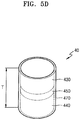
- FIGS. 5A to 5D each illustrate an example of a light-emitting device according to an embodiment.
- a first pixel PX1, a second pixel PX2, and a third pixel PX3 that emit light of different colors from each other may be arranged in the display area DA.
- the first pixel PX1, the second pixel PX2, and the third pixel PX3 may respectively emit, for example, red light, green light, and blue light, or any combination of colors, white light due to combination, etc. Sizes of the pixels may be the same as or different from each other.
- the pixel PX1 may include a first electrode 21, a second electrode 22, and a plurality of light-emitting devices 40 electrically connected to the first electrode 21 and the second electrode 22.
- the pixels PX2 and PX3 may each include a first electrode 21, a second electrode 22, and a plurality of light-emitting devices 40 electrically connected to the respective first electrode 21 and the respective second electrode 22.
- Each of the plurality of light-emitting devices 40 may be a nano-sized light emitting diode (LED).
- the light-emitting device 40 may have various shapes such as a cylinder or a cuboid.
- the light-emitting device 40 may include a first electrode layer 410, a second electrode layer 420, a first semiconductor layer 430, a second semiconductor layer 440, and an active layer 450 between the first semiconductor layer 430 and the second semiconductor layer 440.
- the first electrode layer 410, the first semiconductor layer 430, the active layer 450, the second semiconductor layer 440, and the second electrode layer 420 may be sequentially stacked on one another in a length direction of the light-emitting device 40.
- a length T of the light-emitting device 40 may range between, for example, 1 ⁇ m and 10 ⁇ m, and a diameter of the light-emitting device 40 may range between, for example, 0.5 ⁇ m and 500 ⁇ m.
- the first electrode layer 410 and the second electrode layer 420 may be ohmic contact electrodes, Schottky contact electrodes, etc.
- the first electrode layer 410 and the second electrode layer 420 may each include conductive metal.
- the first electrode layer 410 and the second electrode layer 420 may each include one or more metal materials selected from a group including, for example, aluminum, titanium, indium, gold, and silver.
- the materials included in the first electrode layer 410 and the second electrode layer 420 may be the same as or different from each other.
- the first semiconductor layer 430 may be, for example, an n-type semiconductor layer
- the second semiconductor layer 440 may be, for example, a p-type semiconductor layer.
- the semiconductor layers may each be selected from, for example, GaN, AlN, AlGaN, InGaN, InN, InAlGaN, and AlInN, and may be respectively doped with, for example, an n-type dopant such as Si, Ge, or Sn, a p-type dopant such as Mg, Zn, Ca, Sr, or Ba, etc.
- the first semiconductor layer 430 may include a p-type semiconductor layer
- the second semiconductor layer 440 may include an n-type semiconductor layer.
- the active layer 450 may be between the first semiconductor layer 430 and the second semiconductor layer 440 and may have, for example, a single or multiple quantum well structure.
- the active layer 450 which is an area where electrons and holes recombine, may transition to a low energy level as electrons and holes recombine and may generate light having a wavelength that corresponds thereto.
- a location of the active layer 450 may be variously changed according to the LED type.
- the light-emitting device 40 may further include a fluorescent substance layer, an active layer, a semiconductor layer, and/or an electrode layer on and under the first semiconductor layer 430 and the second semiconductor layer 440.
- the light generated from the active layer 450 may be emitted to an external surface of the light-emitting device 40 (L1, Figure 7 ) and may be emitted to both side surfaces of the light-emitting device 40 (L2 and L3, Figure 7 ).
- the light-emitting device 40 may further include an insulation film 470 that covers an external surface of the light-emitting device 40.
- the insulation film 470 may cover the active layer 450 and thus may prevent an electric short that may occur when the active layer 450 contacts the first electrode 21 or the second electrode 22.
- the insulation film 470 may prevent degradation of luminescent efficiency by protecting the external surface including the active layer 450 of the light-emitting device 40.
- FIG. 5B An embodiment illustrated in FIG. 5B is different from the embodiment of FIG. 5A in which the insulation film 470 covers at least the active layer 450, in that the insulation film 470 covers the entire external surface of the light-emitting device 40, and is the same as the embodiment of FIG. 5A in terms of other configurations.
- the first electrode layer 410 and/or the second electrode layer 420 of the light-emitting device 40 may be omitted.
- An embodiment illustrated in FIG. 5C is an example of the light-emitting device 40 having one of the first electrode layer 410 and the second electrode layer 420, for example, the second electrode layer 420, omitted from the light-emitting device 40 of FIG. 5A and including only the first electrode layer 410.
- the insulation film 470 covers only a portion of an external surface of the first electrode layer 410 and entirely covers an external surface of the second semiconductor layer 440. In another embodiment, the insulation film 470 may cover only a portion of the external surface of the second semiconductor layer 440.
- FIG. 5D An embodiment illustrated in FIG. 5D is an example of the light-emitting device 40 having both the first electrode layer 410 and the second electrode layer 420 omitted.
- the insulation film 470 may cover the entire external surfaces of the first semiconductor layer 430 and the second semiconductor layer 440, or may partially cover and partially expose external surfaces of the first semiconductor layer 430 and the second semiconductor layer 440. In the embodiment of FIG. 5D , the insulation film 470 covers the entire external surfaces of the first semiconductor layer 430 and the second semiconductor layer 440.
- contact areas with the first and second electrodes 21 and 22 and first and second connection electrodes 61 and 62 may increase.
- the plurality of light-emitting devices 40 may each have both ends respectively contacting an upper surface of the first electrode 21 and an upper surface of the second electrode 22, and may be separate from one another on the first electrode 21 and the second electrode 22.
- the first electrode layer 410 or the first semiconductor layer 430 and the second electrode layer 420 or the second semiconductor layer 440, which are outermost layers of both ends of the light-emitting device 40, may respectively contact the upper surface of the first electrode 21 and the upper surface of the second electrode 22.
- the insulation film 470 covers the entire external surface of the light-emitting device 40, the same goes for a case in which the insulation film 470 partially exposes the outermost layers of both ends of the light-emitting device 40.
- the first electrode 21 may be electrically connected to a first electrode line 25 extending in a second direction and may receive an electric signal from the first electrode line 25.
- the first electrode line 25 may be electrically connected to first electrodes 21 of the pixels adjacent to each other in the second direction.
- the second electrode 22 may be electrically connected to a second electrode line 26 extending in a first direction perpendicular to the second direction and may receive an electric signal from the second electrode line 26.
- the second electrode line 26 may be electrically connected to second electrodes 22 of the pixels adjacent to each other in the first direction.
- the first electrode 21 and the second electrode 22 may be reversely disposed.
- FIGS. 6 and 7 are cross-sectional views of the first electrode 21 and the second electrode 22 according to an embodiment.
- the first electrode 21 and the second electrode 22 may face each other in parallel on an insulation surface 110.
- the insulation surface 110 may be the top surface of the substrate 100 having insulating properties, as illustrated in FIG. 3 , or may be the top surface of an insulation layer 105 disposed above the substrate 100, as illustrated in FIG. 4 .
- the first electrode 21 may include a first portion 21a having a flat upper surface that is parallel to the insulation surface 110, and a second portion 21b that protrudes from the first portion 21a and has an inclined surface.
- the first portion 21a may be a mounting part that the light-emitting device 40 contacts, and the second portion 21b may be a reflecting part that reflects light emitted from a side portion of the light-emitting device 40 and changes a path of the light.
- An angle ⁇ 11 between a side surface of the first portion 21a and the upper surface at a boundary where the side surface meets the upper surface may be about 90 degrees.
- An angle ⁇ 12 of the inclined surface of the second portion 21b may range between about 30 degrees and about 60 degrees.
- the angle ⁇ 12 of the inclined surface may be an angle between the upper surface of the first portion 21a and an upper surface of the second portion 21b at a boundary where the upper surface of the first portion 21a meets the upper surface of the second portion 21b.
- the second electrode 22 may include a first portion 22a having a flat upper surface that is parallel to the insulation surface 110, and a second portion 22b that protrudes from the first portion 22a and has an inclined surface.
- An angle ⁇ 21 between a side surface of the first portion 22a and the upper surface at a boundary where the side surface meets the upper surface may be about 90 degrees.
- An angle ⁇ 22 of the inclined surface of the second portion 22b may range between about 30 degrees and about 60 degrees.
- the angle ⁇ 22 of the inclined surface may be an angle between the upper surface of the first portion 22a and an upper surface of the second portion 22b at a boundary where the upper surface of the first portion 22a meets the upper surface of the second portion 22b.
- a separation distance D between the first electrode 21 and the second electrode 22 is less than the length T of the light-emitting device 40.
- a sum of the separation distance D between the first electrode 21 and the second electrode 22 and a length d of the first portion 21a of the first electrode 21 or the first portion 22a of the second electrode 22 is less than the length T of the light-emitting device 40 (D+d ⁇ T), and the separation distance D is less than the length d of the first portion 21a or 22a (D ⁇ d).
- the length d of the first portion 21a of the first electrode 21 or the first portion 22a of the second electrode 22 may be one half to one third of the length T of the light-emitting device 40.
- the length d of the first portion 21a of the first electrode 21 and the length d of the first portion 22a of the second electrode 22 may be the same as or different from each other.
- the length d of the first portion 21a or 22a is a length in the length direction of the light-emitting device 40.
- Heights h of the second portion 21b of the first electrode 21 and the second portion 22b of the second electrode 22 may each be equal to or greater than the diameter of the light-emitting device 40.
- each of the heights h of the second portion 21b of the first electrode 21 and the second portion 22b of the second electrode 22 may be two times greater than the diameter of the light-emitting device 40.
- the first electrode layer 410 and/or the first semiconductor layer 430 of the light-emitting device 40 may contact the upper surface of the first portion 21a of the first electrode 21, and the second electrode layer 420 and/or the second semiconductor layer 440 may contact the upper surface of the first portion 22a of the second electrode 22.
- the first electrode layer 410 or the first semiconductor layer 430 of the light-emitting device 40 may be electrically connected to the first electrode 21 via the first connection electrode 61, and the second electrode layer 420 or the second semiconductor layer 440 may be electrically connected to the second electrode 22 via the second connection electrode 62.
- the first connection electrode 61 may cover an exposed portion of the first electrode layer 410 or the first semiconductor layer 430 of the light-emitting device 40 and an upper surface of the first electrode 21.
- the second connection electrode 62 may cover an exposed portion of the second electrode layer 420 or the second semiconductor layer 440 of the light-emitting device 40 and an upper surface of the second electrode 22.
- light rays L2 and L3 that are emitted to both sides of the light-emitting device 40 may be respectively reflected by the inclined surfaces of the second portion 21b of the first electrode 21 and the second portion 22b of the second electrode 22, and thus, paths of the light rays L2 and L3 may be changed.
- the light rays L2 and L3 that have changed paths may be added to a light ray L1 that is emitted to an upper side of the light-emitting device 40, and thus, light extraction efficiency may be increased, and luminescent efficiency and luminescent intensity may be increased.
- a partition wall 30 that defines a pixel may be formed around the first electrode 21 and the second electrode 22.
- the partition wall 30 may cover an area except a light-emitting portion 70 where light is emitted as the plurality of light-emitting devices 40 are aligned.
- the partition wall 30 may cover the first electrode line 25 and the second electrode line 26.
- each of the pixels PX1, PX2, and PX3 may be electrically connected to the light-emitting devices 40 and may further include a pixel circuit that controls emission of the light-emitting devices 40.
- An embodiment illustrated in FIG. 4 further includes the pixel circuit, compared with an embodiment illustrated in FIG. 3 , and is the same as the embodiment of FIG. 3 in terms of other configurations.
- the pixel circuit may include at least one thin film transistor and at least one capacitor.
- a first thin film transistor 120 and a second thin film transistor 140 that are on a buffer layer 101, and a power line 163, are illustrated.
- the pixel circuit may have various structures.
- the pixel circuit may include two or more thin film transistors and one or more capacitors, and thus, separate wirings may be further formed.
- the first thin film transistor 120 includes a first active layer 121, a first gate electrode 122, a first drain electrode 123, and a first source electrode 124.
- a first gate insulation layer 102 for insulating the first gate electrode 122 and the first active layer 121 from each other may be between the first gate electrode 122 and the first active layer 121.
- the first gate electrode 122 may partially overlap the first active layer 121.
- a second gate insulation layer 103 and an interlayer insulation layer 104 may be between the first gate electrode 122 and the first drain and source electrodes 123 and 124.
- the first thin film transistor 120 may be disposed on a layer below the light-emitting device 40 and may overlap or may not overlap the light-emitting device 40.
- the first thin film transistor 120 may be a driving thin film transistor that drives the light-emitting device 40.
- the second thin film transistor 140 includes a second active layer 141, a second gate electrode 142, a second drain electrode 143, and a second source electrode 144.
- the first gate insulation layer 102 for insulating the second gate electrode 142 and the second active layer 141 from each other may be between the second gate electrode 142 and the second active layer 141.
- the second gate electrode 142 may partially overlap the second active layer 141.
- the second gate insulation layer 103 and the interlayer insulation layer 104 may be between the second gate electrode 142 and the second drain and source electrodes 143 and 144.
- the second thin film transistor 140 may be disposed on a layer below the light-emitting device 40 and may overlap or may not overlap the light-emitting device 40.
- the second thin film transistor 140 may be a switching thin film transistor.
- the power line 163 may be on the same layer as the first gate electrode 122 of the first thin film transistor 120 and the second gate electrode 142 of the second thin film transistor 140.
- the power line 163 may be electrically connected to the second electrode 22 via a connection line 165.
- the second electrode 22 may be electrically connected to the power line 163 and may receive power from the power line 163.
- an auxiliary layer 161 for reducing a step with its surroundings may be included below the power line 163.
- each of the first electrode 21 and the second electrode 22 has bilateral symmetry with respect to a peak of the second portion 21b or 22b.
- an area of the upper surface of the first portion 21a or 22a may not be bilaterally symmetric.
- the first connection electrode 61 and the second connection electrode 62 respectively cover only portions of exposed areas of the upper surfaces of the first electrode 21 and the second electrode 22.
- the first connection electrode 61 and the second connection electrode 62 may respectively cover at least the portions of the exposed areas of the upper surfaces of the first electrode 21 and the second electrode 22 according to external light reflection and properties of materials for the connection electrodes.
- the first connection electrode 61 and the second connection electrode 62 may respectively cover the entire exposed areas of the upper surfaces of the first electrode 21 and the second electrode 22.
- FIGS. 8A to 8K are schematic cross-sectional views of a process of manufacturing a display apparatus, according to an embodiment.
- a pixel circuit may be formed on the substrate 100.
- the substrate 100 may include various materials, such as glass, metal, or plastic.
- the substrate 100 may include a flexible substrate.
- the flexible substrate refers to a substrate that is twisted and bent easily and may be folded or rolled.
- the flexible substrate may include ultra-thin glass, metal, or plastic.
- the buffer layer 101 may be included on the substrate 100.
- the buffer layer 101 may prevent intrusion of an impurity through the substrate 100, may planarize a surface of the substrate 100, and may include a layer or layers including an inorganic material such as silicon nitride (SiN x ) and/or silicon oxide (SiO x ).
- the first thin film transistor 120 and the second thin film transistor 140 may be formed on the buffer layer 101.
- the first thin film transistor 120 may include the first active layer 121, the first gate electrode 122, the first drain electrode 123, and the first source electrode 124.
- the second thin film transistor 140 may include the second active layer 141, the second gate electrode 142, the second drain electrode 143, and the second source electrode 144.
- the first active layer 121 and the second active layer 141 may each be formed on the buffer layer 101 using a semiconductor material.
- the semiconductor material may be an inorganic semiconductor material such as amorphous silicon or polycrystalline silicon, an organic semiconductor material, an oxide semiconductor material, etc.
- Each of the first active layer 121 and the second active layer 141 may include a drain region and a source region that are doped with B or P ion impurities, and a channel region therebetween.
- the first gate insulation layer 102 may be disposed on the buffer layer 101 and may cover the first active layer 121 and the second active layer 141.
- the second gate insulation layer 103 may be disposed on the first gate insulation layer 102 and may cover the first gate electrode 122 and the second gate electrode 142.
- the first gate electrode 122 and the second gate electrode 142 may each be a single layer or multiple layers including, for example, at least one of aluminum (Al), platinum (Pt), lead (Pd), silver (Ag), magnesium (Mg), gold (Au), nickel (Ni), neodymium (Nd), iridium (Ir), chromium (Cr), lithium (Li), calcium (Ca), molybdenum (Mo), titanium (Ti), tungsten (W), or copper (Cu).
- the first gate insulation layer 102 and the second gate insulation layer 103 may each be a layer or layers including an inorganic material.
- the first gate insulation layer 102 may include silicon oxide (SiO 2 ), silicon nitride (SiN x ), silicon oxynitride (SiON), aluminum oxide (Al 2 O 3 ), titanium oxide (TiO 2 ), tantalum oxide (Ta 2 O 5 ), hafnium oxide (HfO 2 ), and/or zinc oxide (ZrO 2 ).
- the interlayer insulation layer 104 may be included, for example, as a layer or layers including an organic material, which is on the second gate insulation layer 103. In another implementation, the interlayer insulation layer 104 may be a layer or layers including an inorganic material. In an implementation, the second gate insulation layer 103 or the interlayer insulation layer 104 may be omitted.
- the first drain electrode 123, the first source electrode 124, the second drain electrode 143, and the second source electrode 144 may be formed on the interlayer insulation layer 104.
- the first drain electrode 123 and the first source electrode 124 may be respectively connected to the drain region and the source region of the first active layer 121 via contact holes formed in the first gate insulation layer 102, the second gate insulation layer 103, and the interlayer insulation layer 104.
- the second drain electrode 143 and the second source electrode 144 may be respectively connected to the drain region and the source region of the second active layer 141 via contact holes formed in the first gate insulation layer 102, the second gate insulation layer 103, and the interlayer insulation layer 104.
- the first drain electrode 123, the first source electrode 124, the second drain electrode 143, and the second source electrode 144 may each include the same material as that of the first and second gate electrodes 122 and 142.
- the first drain electrode 123, the first source electrode 124, the second drain electrode 143, and the second source electrode 144 may include metal, alloys, metal nitrides, conductive metal oxides, transparent conductive materials, etc.
- the auxiliary layer 161 may be formed on the buffer layer 101.
- the auxiliary layer 161 may be formed using, for example, the same material as that of the first active layer 121 and the second active layer 141, simultaneously with the first active layer 121 and the second active layer 141.
- the auxiliary layer 161 may be formed using a different material from that of the first active layer 121 and the second active layer 141, for example, by a different process from that of the first active layer 121 and the second active layer 141.
- the first gate insulation layer 102 may cover the auxiliary layer 161, and the power line 163 overlapping the auxiliary layer 161 may be formed on the first gate insulation layer 102.
- the power line 163 may be formed, for example, using the same material as that of the first and second gate electrodes 122 and 142, simultaneously with the first and second gate electrodes 122 and 142. In another implementation, the power line 163 may be formed using a different material from that of the first and second gate electrodes 122 and 142, for example, by a different process from that of the first and second gate electrodes 122 and 142.
- the second gate insulation layer 103 and the interlayer insulation layer 104 may be disposed on the power line 163, and the connection line 165 may be formed on the interlayer insulation layer 104.
- the connection line 165 may be electrically connected to the power line 163 via a contact hole formed in the second gate insulation layer 103 and the interlayer insulation layer 104.
- a passivation layer 105 that covers the first and second thin film transistors 120 and 140 may be formed on the interlayer insulation layer 104.
- the passivation layer 105 may be a layer or layers including an organic insulation material or an inorganic insulation material.
- the passivation layer 105 may be formed by alternating an organic insulation material and an inorganic insulation material.
- Contact holes CH that expose a portion of the first drain electrode 123 of the first thin film transistor 120 and a portion of the connection line 165 may be formed in the passivation layer 105.
- a first conductive layer 211 and a photosensitive layer PR1 may be sequentially formed on the passivation layer 105 in this stated order, and a mask M may be aligned above the substrate 100.
- the first conductive layer 211 may be, for example, a transparent conductive film that includes at least one transparent conductive oxide selected from a group including indium tin oxide (ITO), indium zinc oxide (IZO), zinc oxide (ZnO), indium oxide (In 2 O 3 ), indium gallium oxide (IGO), and aluminum zinc oxide (AZO).
- the first conductive layer 211 may include at least one metal selected from Ag, Mg, Al, Pt, Pd, Au, Ni, Nd, Ir, Cr, Li, Ca, and an alloy thereof.
- the first conductive layer 211 may fill the contact holes CH of the passivation layer 105.
- the photosensitive layer PR1 may be a positive or negative photosensitive organic material, and in one or more embodiments, the photosensitive layer PR1 will be described as a positive photosensitive organic material.
- the mask M may be a half-tone mask including a light-blocking portion Ma, a light-transmissive portion Mb, and a semi-transmissive portion Mc.
- the light-blocking portion Ma, the semi-transmissive portion Mc, and the light-transmissive portion Mb may be disposed respectively corresponding to an area where the partition wall 30 is formed, an area where the first electrode 21 and the second electrode 22 are formed, and the other areas.
- the semi-transmissive portion Mc may include a light-variable portion where transmittance gradually changes, and the inclined surfaces of the first electrode 21 and the second electrode 22 may be formed by the light-variable portion where light transmittance gradationally changes.
- light may be irradiated on the photosensitive layer PR1 by using the mask M to perform exposure, and insulation patterns 21', 22', and 30' may be formed by developing the exposed photosensitive layer PR1.
- An area of the photosensitive layer PR1 that corresponds to the light-blocking portion Ma may remain as is and form the insulation pattern 30'.
- An area of the photosensitive layer PR1 that corresponds to the light-transmissive portion Mb may be totally removed.
- An area of the photosensitive layer PR1 that corresponds to the semi-transmissive portion Mc may form the insulation patterns 21' and 22', each of which has an area where the photosensitive layer PR1 remains as is, an area where the photosensitive layer PR1 is partially removed, and an inclined area therebetween.
- the first conductive layer 211 may be etched by using the insulation patterns 21', 22', and 30' as a mask to form the first electrode 21, the second electrode 22, the first electrode line 25, and the second electrode line 26.
- the first electrode 21 may be electrically connected to the first drain electrode 123 of the first thin film transistor 120 that is on a layer below the first electrode 21.
- the second electrode 22 may be electrically connected to the power line 163 via the connection line 165 that is on a layer below the second electrode 22.
- the partition wall 30 may be formed in an area except the light-emitting portion 70 that includes the first electrode 21 and the second electrode 22 where the light-emitting device 40 is to be disposed.
- the partition wall 30 may be patterned by forming an opening exposing the light-emitting portion 70 in an organic insulation layer formed entirely over the substrate 100.
- the light-emitting devices 40 may be transferred onto the first electrode 21 and the second electrode 22 by putting a solvent 90, such as ink or paste including a plurality of light-emitting devices 40, into the light-emitting portion 70.
- the solvent 90 may be, for example, at least one of acetone, water, alcohol, toluene, etc.
- the solvent 90 may be any material that may be evaporated by room temperature or heat.
- an electric field E may be generated between the first electrode 21 and the second electrode 22 by applying power V across the first electrode 21 and the second electrode 22.
- the power V may be an external supply source or internal power of the display apparatus 1.
- the power V may be alternating current power that has a predetermined amplitude and cycle, or direct current power.
- the direct current power may be repeatedly applied to the first electrode 21 and the second electrode 22 and thus realized as power that has a predetermined amplitude and cycle.
- a potential difference due to electric polarities assigned to the first electrode 21 and the second electrode 22 may be generated, and thus, the electric field E may be generated.
- Dipolarity is induced to the light-emitting device 40 under the electric field E that is non-uniform, and a force is applied, by dielectrophoretic (DEP) force, to a side of the light-emitting device 40 where a gradient of the electric field E is large or small.
- DEP dielectrophoretic
- the solvent 90 may be evaporated by room temperature or heat, and the light-emitting device 40 may be self-aligned on the first electrode 21 and the second electrode 22 by the DEP force.
- the light-emitting device 40 may be self-aligned in such a manner that both ends of the light-emitting device 40 respectively contact an upper surface of the first portion 21a of the first electrode 21 and an upper surface of the first portion 22a of the second electrode 22.
- a separation distance D' between a first electrode 21" and a second electrode 22" is greater than a length T' of a light-emitting device 40
- the light-emitting device 40" may come into contact with only one of the first electrode 21" and the second electrode 22" by the DEP force, and thus, contact failure may occur.
- the separation distance D between the first electrode 21 and the second electrode 22 is less than the length T of the light-emitting device 40, and accordingly, self-alignment efficiency of the light-emitting device 40 may increase (refer to FIG. 6 ).
- a second conductive layer 611 and a photosensitive layer PR2 may be sequentially formed in the light-emitting portion 70, and the photosensitive layer PR2 may be patterned by using a mask (not shown).
- the photosensitive layer PR2 may be patterned so that only an area of the second conductive layer 611 that excludes an area to be removed may remain.
- the second conductive layer 611 may be formed over the entire surface of the substrate 100, including an area around the light-emitting portion 70.
- the second conductive layer 611 may be a transparent conductive film that includes at least one transparent conductive oxide selected from a group including ITO, IZO, ZnO, In 2 O 3 , IGO, and AZO.
- the second conductive layer 611 may be metal including Ag, Mg, Al, Pt, Pd, Au, Ni, Nd, Ir, Cr, and a compound thereof.
- the photosensitive layer PR2 may be a positive or negative photosensitive organic material.
- the second conductive layer 611 may be patterned by using the patterned photosensitive layer PR2 as a mask to form the first connection electrode 61 and the second connection electrode 62.
- the first connection electrode 61 and the second connection electrode 62 may at least partially cover exposed areas of upper surfaces of the first electrode 21 and the second electrode 22, respectively.
- the first connection electrode 61 may electrically connect one end of the light-emitting device 40 to the first electrode 21.
- the second connection electrode 62 may electrically connect the other end of the light-emitting device 40 to the second electrode 22.
- a conductive material of the second conductive layer 611 that remains between the light-emitting device 40 and the passivation layer 105 may be removed by wet etching of the above patterning process.
- FIG. 8J illustrates a case in which the conductive material of the second conductive layer 611 partially remains after being removed by wet etching.
- an insulation layer 81 may be formed to cover the light-emitting portion 70.
- the insulation layer 81 may be transparent or semi-transparent with respect to a visible wavelength and thus may prevent degradation of light extraction efficiency.
- the insulation layer 81 may include an organic material, for example, epoxy, poly(methyl methacrylate) (PMMA), benzocyclobutene (BCB), polyimide, polyester, etc.
- the insulation layer 81 may insulate the light-emitting device 40 and the passivation layer 105 from each other and thus may prevent an electric short between remaining conductive materials of the second conductive layer 611.
- An optical layer 83 and a protective layer 85 may be sequentially formed on the insulation layer 81.
- the optical layer 83 which may blocks external light, may be formed on the insulation layer 81.
- the optical layer 83 may be an RGB color filter that corresponds to light that is emitted by the pixel PX.
- the color filter may be formed by patterning a color photoresist layer or may be formed by jetting color ink.
- the optical layer 83 may be a polarizing plate.
- the protective layer 85 may be formed on the optical layer 83.
- the protective layer 85 may have an encapsulating function and may be formed over the entire surface of the substrate 100.
- the protective layer 85 may be formed using an organic material or an inorganic material, or may be formed by alternating an inorganic material and an organic material.
- FIGS. 11A to 11D are cross-sectional views each illustrating an example of the first electrode 21 and the second electrode 22 according to an embodiment.
- the left may be the first electrode 21, and the right may be the second electrode 22, or the right may be the first electrode 21, and the left may be the second electrode 22.
- each of the first electrode 21 and the second electrode 22 may include a first portion 221a and a second portion 221b that protrudes from the first portion 221a and has an inclined surface.
- the first portion 221a has a flat upper surface that is parallel to the insulation surface 110.
- a side surface of the first portion 221a and the upper surface of the first portion 221a may form an angle of about 90 degrees at an upper corner of the first portion 221a that is a boundary where the side surface meets the upper surface.
- the first portion 221a and the second portion 221b may have bilateral symmetry with respect to a peak of the second portion 221b.
- a cross-section of the second portion 221b has a semicircle shape, and an angle of inclination ⁇ 3 of the inclined surface continuously changes.
- the angle of inclination ⁇ 3 is an angle that a tangent line touching an upper surface of the second portion 221b forms with the upper surface of the first portion 221a.
- the angle of inclination ⁇ 3 is 90 degrees at a boundary where the upper surface of the first portion 221a meets the upper surface of the second portion 221b.
- the angle of inclination ⁇ 3 is 0 degrees at the peak of the second portion 221b.
- the angle of inclination ⁇ 3 continuously decreases from 90 degrees to 0 degrees in a direction from the boundary where the upper surface of the first portion 221a meets the upper surface of the second portion 221b to the peak of the second portion 221b.
- the second portion 221b may have a round shape, and thus a uniform electric field may be generated around the second portion 221b, and the DEP force may be concentrated on the first portion 221a. Accordingly, an effect of self-aligning the light-emitting device 40 onto the upper surface of the first portion 221a may be improved. Light that is emitted to a side surface of the light-emitting device 40 may be reflected by the second portion 221 b and be extracted in an upward direction.
- one of the first electrode 21 and the second electrode 22 may be a round-shaped electrode as illustrated in FIG. 11A , and the other may be an electrode having a sharp second portion 321b, the second portion 321b protruding from a first portion 321a.
- the right may be an electrode having a round second portion
- the left may be an electrode having a sharp second portion.
- the first portion 321a of the left electrode has a flat upper surface that is parallel to the insulation surface 110.
- a side surface and the upper surface of the first portion 321a may form an angle of about 90 degrees at an upper corner of the first portion 321 a that is a boundary where the side surface meets the upper surface.
- a cross-section of the second portion 321b of the left electrode may have a right-angled triangle shape, and the second portion 321b may include a first inclined surface 321b1 on a side of the light-emitting device 40 and a second inclined surface 321b2 on an opposite side of the light-emitting device 40.
- An angle of inclination ⁇ 31 of the first inclined surface 321b1, which is an angle that the first inclined surface 321b1 forms with the upper surface of the first portion 321a, is 90 degrees.
- An angle of inclination ⁇ 32 of the second inclined surface 321b2, which is an angle that the second inclined surface 321b2 forms with the upper surface of the first portion 321a, is between 0 degrees and 90 degrees.
- the DEP force is relatively large at an upper corner of the first portion 321a and at a boundary where the first inclined surface 321b1 and the second inclined surface 321b2 meet each other. Accordingly, as the DEP force may be concentrated on the left electrode rather than on the right electrode, the plurality of light-emitting devices 40 may be aligned with the left electrode. Thus, the plurality of light-emitting devices 40 may be regularly self-aligned.
- each of the first electrode 21 and the second electrode 22 may be an electrode having a partially round-shaped second portion 421b, the second portion 421b protruding from a first portion 421a.
- the first portion 421a has a flat upper surface that is parallel to the insulation surface 110.
- a side surface and the upper surface of the first portion 421a may form an angle of about 90 degrees at an upper corner of the first portion 421a that is a boundary where the side surface meets the upper surface.
- a cross-section of the second portion 421b may have a fan shape, and the second portion 421b may include a first inclined surface 421b1 on a side of the light-emitting device 40 and a second inclined surface 421b2 on an opposite side of the light-emitting device 40.
- An angle of inclination ⁇ 31 of the first inclined surface 421b1 is an angle that a tangent line touching the first inclined surface 421b1 forms with the upper surface of the first portion 421a.
- the angle of inclination ⁇ 31 is 90 degrees at a boundary where the upper surface of the first portion 421a meets the first inclined surface 421b1.
- the angle of inclination ⁇ 31 is 0 degrees at the top of the first inclined surface 421b1.
- the angle of inclination ⁇ 31 gradually decreases from 90 degrees to 0 degrees in a direction from the boundary where the upper surface of the first portion 421a meets the first inclined surface 421b1 to the top of the first inclined surface 421b1.
- An angle of inclination ⁇ 32 of the second inclined surface 421b2, which is an angle that the second inclined surface 421b2 forms with the upper surface of the first portion 421a, is 90 degrees.
- Light that is emitted to a side surface of the light-emitting device 40 may be reflected by the first inclined surface 421b1 of the second portion 421b and be extracted in an upward direction.
- each of the first electrode 21 and the second electrode 22 may be an electrode having a sharp second portion 521b, the second portion 521b protruding from a first portion 521a.
- the first portion 521a has a flat upper surface that is parallel to the insulation surface 110.
- a side surface and the upper surface of the first portion 521 a may form an angle of about 90 degrees at an upper corner of the first portion 521a that is a boundary where the side surface meets the upper surface.
- a cross-section of the second portion 521b may have a right-angled triangle shape, and the second portion 521b may include a first inclined surface 521b1 on a side of the light-emitting device 40 and a second inclined surface 521b2 on an opposite side of the light-emitting device 40.
- Light that is emitted to a side surface of the light-emitting device 40 may be reflected by the first inclined surface 521b1 of the second portion 521b and be extracted in an upward direction.
- the first electrode 21 and the second electrode 22 illustrated in FIGS. 11C and 11D may have external light reflection decreased by reducing an area of inclination on the opposite side of the light-emitting device 40.
- FIG. 12 is a plan view of a portion of the display area DA according to an embodiment.
- FIG. 13 is partial cross-sectional view taken along line B-B' of FIG. 12 .
- the pixel PX may be on the insulation surface 110 of the display area DA illustrated in FIG. 1 .
- the insulation surface 110 may be the top surface of the insulating substrate 100, as illustrated in FIG. 3 , or may be the top surface of the insulation layer 105 disposed above the substrate 100, as illustrated in FIG. 4 .
- the pixel PX may be the first pixel PX1 that emits red light, the second pixel PX2 that emits green light, or the third pixel PX3 that emits blue light. However, the disclosure is not limited thereto, and the pixel PX may emit light of another color.
- the pixel PX may include the first electrode 21, the second electrode 22, and the plurality of light-emitting devices 40 electrically connected to the first electrode 21 and the second electrode 22.
- the first electrode 21 may be electrically connected to the first electrode line 25 extending in a second direction and may receive an electric signal from the first electrode line 25.
- the first electrode line 25 may be electrically connected to the first electrodes 21 of the pixels adjacent to each other in the second direction.
- the first electrode 21 may include a plurality of first sub-electrodes 21-2 that have comb shapes and a first main electrode 21-1 that connects the plurality of first sub electrodes 21-2 to each other.
- the second electrode 22 may be electrically connected to the second electrode line 26 extending in a first direction perpendicular to the second direction and may receive an electric signal from the second electrode line 26.
- the second electrode line 26 may be electrically connected to the second electrodes 22 of the pixels adjacent to each other in the first direction.
- the second electrode 22 may include a plurality of second sub electrodes 22-2 that have comb shapes and a second main electrode 22-1 that connects the plurality of second sub electrodes 22-2 to each other.
- the plurality of first sub electrodes 21-2 and the plurality of second sub electrodes 22-2 may be arranged in the first direction while alternating with each other.
- the separation distance D between a first sub electrode 21-2 and a second sub electrode 22-2 is less than the length T of the light-emitting device 40.
- Both ends of each of the plurality of light-emitting devices 40 respectively contact upper surfaces of first portions 21 a-2 and 22a-2 of the first sub electrode 21-2 and the second sub electrode 22-2.
- One end of the light-emitting device 40 may be electrically connected to the first sub electrode 21-2 by the first connection electrode 61, and the other end may be electrically connected to the second sub electrode 22-2 by the second connection electrode 62.
- the partition wall 30 that defines a pixel may be formed around the first electrode 21 and the second electrode 22.
- the partition wall 30 may cover an area excluding the light-emitting portion 70 where light is emitted as the plurality of light-emitting devices 40 are aligned.
- the partition wall 30 may cover the first electrode line 25, the second electrode line 26, the first main electrode 21-1, and the second main electrode 22-1.
- Light that is emitted to a side surface of the light-emitting device 40 may be reflected by inclined surfaces of second portions 21b-2 and 22b-2 and be extracted in an upward direction.
- pixels PX that emit light of the same color may share the first electrode 21 and/or the second electrode 22, and the first electrode 21 and the second electrode 22 may have bilateral symmetry.
- the first electrode 21 and the second electrode 22 have various types of electrode structures disclosed in FIGS. 11A to 11D
- the pixels PX that emit light of the same color may share the first electrode 21 and/or the second electrode 22.
- placement and arrangement of the first electrode and the second electrode may have various layouts according to the size and density of the light-emitting devices.
- a distance between a pair of electrodes on which a light-emitting device is seated is less than a length of the light-emitting device
- each of the pair of electrodes may include a first portion on which the DEP force is concentrated and a second portion that changes, as a reflecting member, a path of light that is emitted to a side portion of the light-emitting device.
- self-alignment of light-emitting devices may be induced by using a pair of electrodes having both an electrode function and a reflection function, and thus placement and arrangement of the light-emitting devices may be concentrated on the pair of electrodes.
- methods of arranging the LED and the electrode include a method of directly growing the LED, and a method of independently growing the LED separately and then arranging the LED relative to the electrode.
- a method of directly growing the LED and a method of independently growing the LED separately and then arranging the LED relative to the electrode.
- embodiments include a display apparatus and a method of manufacturing the same, whereby nano-sized, microminiature light-emitting devices that are independently manufactured may be aligned and connected to each other between two different electrodes, and thus, an abnormal alignment error of the microminiature light-emitting devices may be reduced or prevented.
Landscapes
- Engineering & Computer Science (AREA)
- Microelectronics & Electronic Packaging (AREA)
- Manufacturing & Machinery (AREA)
- Electroluminescent Light Sources (AREA)
- Devices For Indicating Variable Information By Combining Individual Elements (AREA)
Abstract
Description
- Embodiments of the invention relate to a display apparatus and a method of manufacturing the same.
- In general, a light-emitting diode (LED) has a high light conversion efficiency, consumes a very small amount of energy, can be used semi-permanently, and is eco-friendly. To use the LED in lighting, displays, and the like, the LED and an electrode that is capable of applying power to the LED are connected to each other.
- Embodiments of the invention are directed to a display apparatus, including a substrate, a first electrode on the substrate, the first electrode including a first portion that has a flat upper surface and a second portion that protrudes from the first portion and has an inclined surface, a second electrode facing the first electrode in parallel on the substrate, the second electrode including a first portion that has a flat upper surface and a second portion that protrudes from the first portion and has an inclined surface, and a plurality of light-emitting devices separate from each other on the first electrode and the second electrode, the light-emitting devices each having a first end contacting the upper surface of the first portion of the first electrode and a second end contacting the upper surface of the first portion of the second electrode.
- A distance between the first electrode and the second electrode may be less than a length of each of the plurality of light-emitting devices.
- An angle of the inclined surface of the second portion may range between about 30 degrees and about 60 degrees.
- An angle of the inclined surface of the second portion of at least one selected from the first electrode and the second electrode may continuously change.
- An angle of the inclined surface of the second portion of at least one selected from the first electrode and the second electrode may be 90 degrees.
- The inclined surface of the second portion may include a first inclined surface on a side of each of the plurality of light-emitting devices and a second inclined surface on an opposite side of each of the plurality of light-emitting devices.
- At least one selected from the first electrode and the second electrode may have the first inclined surface that has an angle of 90 degrees and the second inclined surface that has an angle ranging between 0 degrees and 90 degrees.
- A cross-section of the second portion of at least one selected from the first electrode and the second electrode may have a semicircle shape.
- A cross-section of the second portion of at least one selected from the first electrode and the second electrode may have a right-angled triangle shape.
- The first portion and the second portion may have bilateral symmetry.
- The display apparatus may further include a first connection electrode that contacts the first end of each of the plurality of light-emitting devices and the first electrode, and a second connection electrode that contacts the second end of each of the plurality of light-emitting devices and the second electrode.
- The first connection electrode may cover at least a portion of an exposed upper surface of the first electrode, and the second connection electrode may cover at least a portion of an exposed upper surface of the second electrode.
- The display apparatus may further include a thin film transistor connected to one selected from the first electrode and the second electrode, and a power line connected to one selected from the first electrode and the second electrode.
- A sum of a length of the first portion of one selected from the first electrode and the second electrode and a distance between the first electrode and the second electrode may be less than a length of each of the plurality of light-emitting devices.
- A height of the second portion may be equal to or greater than a diameter of each of the plurality of light-emitting devices.
- Embodiments are also directed to a method of manufacturing a display apparatus, the method including forming a first conductive layer on an insulation surface, forming, by patterning the first conductive layer, a pair of a first electrode and a second electrode having first portions that have flat upper surfaces and second portions that protrude from the first portions and have inclined surfaces, applying, onto the first electrode and the second electrode, a solvent including a plurality of light-emitting devices, and aligning the plurality of light-emitting devices by assigning different electric polarities to the first electrode and the second electrode so that two ends of each of the plurality of light-emitting devices respectively contact the upper surfaces of the first portions of the first electrode and the second electrode.
- An electric field may be generated between the first electrode and the second electrode due to the electric polarities assigned to the first electrode and the second electrode, and an electric field gradient at an upper corner of each of the first portions of the first electrode and the second electrode may be greater than that at a top of each of the second portions of the first and second electrodes.
- A cross-section of the second portion of at least one selected from the first electrode and the second electrode may have a semicircle shape.
- The method may further include forming a second conductive layer that covers the plurality of light-emitting devices and the pair of electrodes, and forming, by patterning the second conductive layer, a first connection electrode that contacts a first end of each of the plurality of light-emitting devices and the first electrode, and a second connection electrode that contacts a second end of each of the plurality of light-emitting devices and the second electrode.
- The forming of the first electrode and the second electrode may include disposing, above the first conductive layer, a mask that has a gradually variable light transmittance in areas of the mask that correspond to the inclined surfaces of the second portions, and patterning the first conductive layer by using the mask.
- At least some of the above features and other features according to the invention are set out in the claims.
- Features will be made more apparent to those of skill in the art by describing in detail example embodiments of the invention with reference to the attached drawings in which:
-
FIG. 1 illustrates a schematic plan view of a display apparatus according to an embodiment; -
FIG. 2 illustrates a plan view of a portion of a display area according to an embodiment; -
FIGS. 3 and4 illustrate partial cross-sectional views taken along line A-A' ofFIG. 2 ; -
FIGS. 5A to 5D each illustrate an example of a light-emitting device according to an embodiment; -
FIGS. 6 and7 illustrate cross-sectional views of a first electrode and a second electrode according to an embodiment; -
FIGS. 8A to 8K illustrate schematic cross-sectional views of a process of manufacturing a display apparatus, according to an embodiment; -
FIG. 9 illustrates an example diagram illustrating self-alignment of a light-emitting device according to an embodiment; -
FIG. 10 illustrates a cross-sectional view of a comparative example; -
FIGS. 11A to 11D illustrate cross-sectional views each illustrating an example of a first electrode and a second electrode according to an embodiment; -
FIG. 12 illustrates a plan view of a portion of a display area according to an embodiment; and -
FIG. 13 illustrates partial cross-sectional view taken along line B-B' ofFIG. 12 . - Example embodiments of the invention will now be described more fully hereinafter with reference to the accompanying drawings; however, the invention may be embodied in different forms and should not be construed as limited to the embodiments set forth herein. Rather, these embodiments are provided so that this disclosure will be thorough, and will convey example implementations to those skilled in the art.
- In the drawing figures, the dimensions of layers and regions may be exaggerated for clarity of illustration. Like reference numerals refer to like elements throughout.
- While such terms as "first" and "second" may be used to describe various elements, such elements must not be limited to the above terms. The above terms are used only to distinguish one element from another.
- It will be understood that the singular forms "a", "an", and "the" are intended to include the plural forms as well, unless the context clearly indicates otherwise.
- It will be further understood that the terms such as "include", "comprise", and "have" used herein specify the presence of stated features or elements, but do not preclude the presence or addition of one or more other features or elements.
- Sizes of elements in the drawings may be exaggerated for convenience of explanation. In other words, since sizes and thicknesses of elements in the drawings are arbitrarily illustrated for convenience of explanation, one or more embodiments are not limited thereto.
- In the following examples, the x-axis, the y-axis, and the z-axis are not limited to three axes of the rectangular coordinate system and may be interpreted in a broader sense. For example, the x-axis, the y-axis, and the z-axis may be perpendicular to one another or may represent different directions that are not perpendicular to one another.
- When an embodiment may be implemented differently, a specific process order may be performed differently from the described order. For example, two consecutively described processes may be performed substantially at the same time or performed in an order opposite to the described order.
- The term "corresponding" or "corresponding to" used herein may refer to being disposed in or connected to the same column or row, according to the context. For example, when a first member is referred to as being connected to a "corresponding" second member from among a plurality of second members, the first member may be connected to the second member that is disposed in the same column or the same row as that of the first member.
- As used herein, the term "and/or" includes any and all combinations of one or more of the associated listed items. Expressions such as "at least one of," when preceding a list of elements, modify the entire list of elements and do not modify the individual elements of the list.
-
FIG. 1 is a schematic plan view of a display apparatus 1 according to an embodiment. - Referring to
FIG. 1 , the display apparatus 1 may include asubstrate 100 that has a display area DA. A plurality of scan lines SL and a plurality of data lines DL may be arranged in the display area DA of thesubstrate 100. The plurality of scan lines SL are separate from each other in a predetermined direction and transmit scan signals to pixels. The plurality of data lines DL are separate from each other in a predetermined direction and transmit data signals to pixels. An extension direction of the plurality of scan lines SL may be the same as or different from an extension direction of the plurality of data lines DL. For example, the extension direction of the plurality of scan lines SL may be perpendicular to the extension direction of the plurality of data lines DL. - Pixels P may each be connected to a corresponding scan line SL and a corresponding data line DL. A plurality of pixels P may be arranged on the
substrate 100 in various patterns such as a matrix form or a zigzag form. Each pixel P may emit one color, for example, one of red, blue, green, and white, or another color besides red, blue, green, and white. - A non-display area NA may be defined in an area around the display area DA, that is, a peripheral area of the display area DA. A
first driver 200 and asecond driver 300 may be arranged in the non-display area NA. - The
first driver 200 may generate data signals and may supply the data signals to the plurality of data lines DL arranged in the display area DA. - The
second driver 300 may generate scan signals and may supply the scan signals to the plurality of scan lines SL arranged in the display area DA. - The
first driver 200 and thesecond driver 300, which are driving circuits, may be formed as integrated circuit chips and mounted on thesubstrate 100, or may be directly formed on thesubstrate 100 together when the pixels P of the display area DA are formed. -
FIG. 2 is a plan view of a portion of the display area DA according to an embodiment.FIGS. 3 and4 are partial cross-sectional views taken along line A-A' ofFIG. 2 .FIGS. 5A to 5D each illustrate an example of a light-emitting device according to an embodiment. - Referring to
FIGS. 2 and3 together, a first pixel PX1, a second pixel PX2, and a third pixel PX3 that emit light of different colors from each other may be arranged in the display area DA. The first pixel PX1, the second pixel PX2, and the third pixel PX3 may respectively emit, for example, red light, green light, and blue light, or any combination of colors, white light due to combination, etc. Sizes of the pixels may be the same as or different from each other. - The pixel PX1 may include a
first electrode 21, asecond electrode 22, and a plurality of light-emittingdevices 40 electrically connected to thefirst electrode 21 and thesecond electrode 22. Similarly, the pixels PX2 and PX3 may each include afirst electrode 21, asecond electrode 22, and a plurality of light-emittingdevices 40 electrically connected to the respectivefirst electrode 21 and the respectivesecond electrode 22. - Each of the plurality of light-emitting
devices 40 may be a nano-sized light emitting diode (LED). The light-emittingdevice 40 may have various shapes such as a cylinder or a cuboid. - Referring to
FIG. 5A , the light-emittingdevice 40 according to an embodiment may include afirst electrode layer 410, asecond electrode layer 420, afirst semiconductor layer 430, asecond semiconductor layer 440, and anactive layer 450 between thefirst semiconductor layer 430 and thesecond semiconductor layer 440. As an example, thefirst electrode layer 410, thefirst semiconductor layer 430, theactive layer 450, thesecond semiconductor layer 440, and thesecond electrode layer 420 may be sequentially stacked on one another in a length direction of the light-emittingdevice 40. A length T of the light-emittingdevice 40 may range between, for example, 1 µm and 10 µm, and a diameter of the light-emittingdevice 40 may range between, for example, 0.5 µm and 500 µm. - The
first electrode layer 410 and thesecond electrode layer 420 may be ohmic contact electrodes, Schottky contact electrodes, etc. Thefirst electrode layer 410 and thesecond electrode layer 420 may each include conductive metal. For example, thefirst electrode layer 410 and thesecond electrode layer 420 may each include one or more metal materials selected from a group including, for example, aluminum, titanium, indium, gold, and silver. The materials included in thefirst electrode layer 410 and thesecond electrode layer 420 may be the same as or different from each other. - The
first semiconductor layer 430 may be, for example, an n-type semiconductor layer, and thesecond semiconductor layer 440 may be, for example, a p-type semiconductor layer. The semiconductor layers may each be selected from, for example, GaN, AlN, AlGaN, InGaN, InN, InAlGaN, and AlInN, and may be respectively doped with, for example, an n-type dopant such as Si, Ge, or Sn, a p-type dopant such as Mg, Zn, Ca, Sr, or Ba, etc. In an implementation, thefirst semiconductor layer 430 may include a p-type semiconductor layer, and thesecond semiconductor layer 440 may include an n-type semiconductor layer. - The
active layer 450 may be between thefirst semiconductor layer 430 and thesecond semiconductor layer 440 and may have, for example, a single or multiple quantum well structure. Theactive layer 450, which is an area where electrons and holes recombine, may transition to a low energy level as electrons and holes recombine and may generate light having a wavelength that corresponds thereto. A location of theactive layer 450 may be variously changed according to the LED type. In an implementation, the light-emittingdevice 40 may further include a fluorescent substance layer, an active layer, a semiconductor layer, and/or an electrode layer on and under thefirst semiconductor layer 430 and thesecond semiconductor layer 440. The light generated from theactive layer 450 may be emitted to an external surface of the light-emitting device 40 (L1,Figure 7 ) and may be emitted to both side surfaces of the light-emitting device 40 (L2 and L3,Figure 7 ). - The light-emitting
device 40 may further include aninsulation film 470 that covers an external surface of the light-emittingdevice 40. As an example, theinsulation film 470 may cover theactive layer 450 and thus may prevent an electric short that may occur when theactive layer 450 contacts thefirst electrode 21 or thesecond electrode 22. Also, theinsulation film 470 may prevent degradation of luminescent efficiency by protecting the external surface including theactive layer 450 of the light-emittingdevice 40. - An embodiment illustrated in
FIG. 5B is different from the embodiment ofFIG. 5A in which theinsulation film 470 covers at least theactive layer 450, in that theinsulation film 470 covers the entire external surface of the light-emittingdevice 40, and is the same as the embodiment ofFIG. 5A in terms of other configurations. - The
first electrode layer 410 and/or thesecond electrode layer 420 of the light-emittingdevice 40 may be omitted. An embodiment illustrated inFIG. 5C is an example of the light-emittingdevice 40 having one of thefirst electrode layer 410 and thesecond electrode layer 420, for example, thesecond electrode layer 420, omitted from the light-emittingdevice 40 ofFIG. 5A and including only thefirst electrode layer 410. In the light-emittingdevice 40 ofFIG. 5C , theinsulation film 470 covers only a portion of an external surface of thefirst electrode layer 410 and entirely covers an external surface of thesecond semiconductor layer 440. In another embodiment, theinsulation film 470 may cover only a portion of the external surface of thesecond semiconductor layer 440. - An embodiment illustrated in
FIG. 5D is an example of the light-emittingdevice 40 having both thefirst electrode layer 410 and thesecond electrode layer 420 omitted. Theinsulation film 470 may cover the entire external surfaces of thefirst semiconductor layer 430 and thesecond semiconductor layer 440, or may partially cover and partially expose external surfaces of thefirst semiconductor layer 430 and thesecond semiconductor layer 440. In the embodiment ofFIG. 5D , theinsulation film 470 covers the entire external surfaces of thefirst semiconductor layer 430 and thesecond semiconductor layer 440. - When the
insulation film 470 exposes the electrode layer or the semiconductor layer, contact areas with the first andsecond electrodes second connection electrodes - The plurality of light-emitting
devices 40 may each have both ends respectively contacting an upper surface of thefirst electrode 21 and an upper surface of thesecond electrode 22, and may be separate from one another on thefirst electrode 21 and thesecond electrode 22. Thefirst electrode layer 410 or thefirst semiconductor layer 430 and thesecond electrode layer 420 or thesecond semiconductor layer 440, which are outermost layers of both ends of the light-emittingdevice 40, may respectively contact the upper surface of thefirst electrode 21 and the upper surface of thesecond electrode 22. - Although, for convenience of description, reference will now be made to the drawing in which the
insulation film 470 covers the entire external surface of the light-emittingdevice 40, the same goes for a case in which theinsulation film 470 partially exposes the outermost layers of both ends of the light-emittingdevice 40. - The
first electrode 21 may be electrically connected to afirst electrode line 25 extending in a second direction and may receive an electric signal from thefirst electrode line 25. Thefirst electrode line 25 may be electrically connected tofirst electrodes 21 of the pixels adjacent to each other in the second direction. - The
second electrode 22 may be electrically connected to asecond electrode line 26 extending in a first direction perpendicular to the second direction and may receive an electric signal from thesecond electrode line 26. Thesecond electrode line 26 may be electrically connected tosecond electrodes 22 of the pixels adjacent to each other in the first direction. Thefirst electrode 21 and thesecond electrode 22 may be reversely disposed. -
FIGS. 6 and7 are cross-sectional views of thefirst electrode 21 and thesecond electrode 22 according to an embodiment. - Referring to
FIG. 6 , thefirst electrode 21 and thesecond electrode 22 may face each other in parallel on aninsulation surface 110. Theinsulation surface 110 may be the top surface of thesubstrate 100 having insulating properties, as illustrated inFIG. 3 , or may be the top surface of aninsulation layer 105 disposed above thesubstrate 100, as illustrated inFIG. 4 . - The
first electrode 21 may include afirst portion 21a having a flat upper surface that is parallel to theinsulation surface 110, and asecond portion 21b that protrudes from thefirst portion 21a and has an inclined surface. Thefirst portion 21a may be a mounting part that the light-emittingdevice 40 contacts, and thesecond portion 21b may be a reflecting part that reflects light emitted from a side portion of the light-emittingdevice 40 and changes a path of the light. An angle θ11 between a side surface of thefirst portion 21a and the upper surface at a boundary where the side surface meets the upper surface may be about 90 degrees. An angle θ12 of the inclined surface of thesecond portion 21b may range between about 30 degrees and about 60 degrees. The angle θ12 of the inclined surface may be an angle between the upper surface of thefirst portion 21a and an upper surface of thesecond portion 21b at a boundary where the upper surface of thefirst portion 21a meets the upper surface of thesecond portion 21b. - Likewise, the
second electrode 22 may include afirst portion 22a having a flat upper surface that is parallel to theinsulation surface 110, and asecond portion 22b that protrudes from thefirst portion 22a and has an inclined surface. An angle θ21 between a side surface of thefirst portion 22a and the upper surface at a boundary where the side surface meets the upper surface may be about 90 degrees. An angle θ22 of the inclined surface of thesecond portion 22b may range between about 30 degrees and about 60 degrees. The angle θ22 of the inclined surface may be an angle between the upper surface of thefirst portion 22a and an upper surface of thesecond portion 22b at a boundary where the upper surface of thefirst portion 22a meets the upper surface of thesecond portion 22b. - A separation distance D between the
first electrode 21 and thesecond electrode 22 is less than the length T of the light-emittingdevice 40. A sum of the separation distance D between thefirst electrode 21 and thesecond electrode 22 and a length d of thefirst portion 21a of thefirst electrode 21 or thefirst portion 22a of thesecond electrode 22 is less than the length T of the light-emitting device 40 (D+d<T), and the separation distance D is less than the length d of thefirst portion first portion 21a of thefirst electrode 21 or thefirst portion 22a of thesecond electrode 22 may be one half to one third of the length T of the light-emittingdevice 40. The length d of thefirst portion 21a of thefirst electrode 21 and the length d of thefirst portion 22a of thesecond electrode 22 may be the same as or different from each other. The length d of thefirst portion device 40. - Heights h of the
second portion 21b of thefirst electrode 21 and thesecond portion 22b of thesecond electrode 22 may each be equal to or greater than the diameter of the light-emittingdevice 40. For example, each of the heights h of thesecond portion 21b of thefirst electrode 21 and thesecond portion 22b of thesecond electrode 22 may be two times greater than the diameter of the light-emittingdevice 40. - The
first electrode layer 410 and/or thefirst semiconductor layer 430 of the light-emittingdevice 40 may contact the upper surface of thefirst portion 21a of thefirst electrode 21, and thesecond electrode layer 420 and/or thesecond semiconductor layer 440 may contact the upper surface of thefirst portion 22a of thesecond electrode 22. - The
first electrode layer 410 or thefirst semiconductor layer 430 of the light-emittingdevice 40 may be electrically connected to thefirst electrode 21 via thefirst connection electrode 61, and thesecond electrode layer 420 or thesecond semiconductor layer 440 may be electrically connected to thesecond electrode 22 via thesecond connection electrode 62. Thefirst connection electrode 61 may cover an exposed portion of thefirst electrode layer 410 or thefirst semiconductor layer 430 of the light-emittingdevice 40 and an upper surface of thefirst electrode 21. Thesecond connection electrode 62 may cover an exposed portion of thesecond electrode layer 420 or thesecond semiconductor layer 440 of the light-emittingdevice 40 and an upper surface of thesecond electrode 22. - Referring to
FIG. 7 , light rays L2 and L3 that are emitted to both sides of the light-emittingdevice 40 may be respectively reflected by the inclined surfaces of thesecond portion 21b of thefirst electrode 21 and thesecond portion 22b of thesecond electrode 22, and thus, paths of the light rays L2 and L3 may be changed. The light rays L2 and L3 that have changed paths may be added to a light ray L1 that is emitted to an upper side of the light-emittingdevice 40, and thus, light extraction efficiency may be increased, and luminescent efficiency and luminescent intensity may be increased. - Referring to
FIG. 3 again, apartition wall 30 that defines a pixel may be formed around thefirst electrode 21 and thesecond electrode 22. Thepartition wall 30 may cover an area except a light-emittingportion 70 where light is emitted as the plurality of light-emittingdevices 40 are aligned. Thepartition wall 30 may cover thefirst electrode line 25 and thesecond electrode line 26. - As illustrated in
FIG. 4 , each of the pixels PX1, PX2, and PX3 may be electrically connected to the light-emittingdevices 40 and may further include a pixel circuit that controls emission of the light-emittingdevices 40. An embodiment illustrated inFIG. 4 further includes the pixel circuit, compared with an embodiment illustrated inFIG. 3 , and is the same as the embodiment ofFIG. 3 in terms of other configurations. - The pixel circuit may include at least one thin film transistor and at least one capacitor. In the embodiment of
FIG. 4 , a firstthin film transistor 120 and a secondthin film transistor 140 that are on abuffer layer 101, and apower line 163, are illustrated. The pixel circuit may have various structures. For example, the pixel circuit may include two or more thin film transistors and one or more capacitors, and thus, separate wirings may be further formed. - The first
thin film transistor 120 includes a firstactive layer 121, afirst gate electrode 122, afirst drain electrode 123, and afirst source electrode 124. A firstgate insulation layer 102 for insulating thefirst gate electrode 122 and the firstactive layer 121 from each other may be between thefirst gate electrode 122 and the firstactive layer 121. On the firstgate insulation layer 102, thefirst gate electrode 122 may partially overlap the firstactive layer 121. A secondgate insulation layer 103 and aninterlayer insulation layer 104 may be between thefirst gate electrode 122 and the first drain andsource electrodes thin film transistor 120 may be disposed on a layer below the light-emittingdevice 40 and may overlap or may not overlap the light-emittingdevice 40. The firstthin film transistor 120 may be a driving thin film transistor that drives the light-emittingdevice 40. - The second
thin film transistor 140 includes a secondactive layer 141, asecond gate electrode 142, asecond drain electrode 143, and asecond source electrode 144. The firstgate insulation layer 102 for insulating thesecond gate electrode 142 and the secondactive layer 141 from each other may be between thesecond gate electrode 142 and the secondactive layer 141. On the firstgate insulation layer 102, thesecond gate electrode 142 may partially overlap the secondactive layer 141. The secondgate insulation layer 103 and theinterlayer insulation layer 104 may be between thesecond gate electrode 142 and the second drain andsource electrodes thin film transistor 140 may be disposed on a layer below the light-emittingdevice 40 and may overlap or may not overlap the light-emittingdevice 40. The secondthin film transistor 140 may be a switching thin film transistor. - The
power line 163 may be on the same layer as thefirst gate electrode 122 of the firstthin film transistor 120 and thesecond gate electrode 142 of the secondthin film transistor 140. Thepower line 163 may be electrically connected to thesecond electrode 22 via aconnection line 165. Accordingly, thesecond electrode 22 may be electrically connected to thepower line 163 and may receive power from thepower line 163. In an implementation, anauxiliary layer 161 for reducing a step with its surroundings may be included below thepower line 163. - In the aforesaid embodiment, each of the
first electrode 21 and thesecond electrode 22 has bilateral symmetry with respect to a peak of thesecond portion first portion - In the aforesaid embodiment, the
first connection electrode 61 and thesecond connection electrode 62 respectively cover only portions of exposed areas of the upper surfaces of thefirst electrode 21 and thesecond electrode 22. In another implementation, thefirst connection electrode 61 and thesecond connection electrode 62 may respectively cover at least the portions of the exposed areas of the upper surfaces of thefirst electrode 21 and thesecond electrode 22 according to external light reflection and properties of materials for the connection electrodes. For example, thefirst connection electrode 61 and thesecond connection electrode 62 may respectively cover the entire exposed areas of the upper surfaces of thefirst electrode 21 and thesecond electrode 22. -
FIGS. 8A to 8K are schematic cross-sectional views of a process of manufacturing a display apparatus, according to an embodiment. - Referring to
FIG. 8A , a pixel circuit may be formed on thesubstrate 100. - The
substrate 100 may include various materials, such as glass, metal, or plastic. According to an embodiment, thesubstrate 100 may include a flexible substrate. In this regard, the flexible substrate refers to a substrate that is twisted and bent easily and may be folded or rolled. The flexible substrate may include ultra-thin glass, metal, or plastic. - In an implementation, the
buffer layer 101 may be included on thesubstrate 100. Thebuffer layer 101 may prevent intrusion of an impurity through thesubstrate 100, may planarize a surface of thesubstrate 100, and may include a layer or layers including an inorganic material such as silicon nitride (SiNx) and/or silicon oxide (SiOx). - The first
thin film transistor 120 and the secondthin film transistor 140 may be formed on thebuffer layer 101. - The first
thin film transistor 120 may include the firstactive layer 121, thefirst gate electrode 122, thefirst drain electrode 123, and thefirst source electrode 124. The secondthin film transistor 140 may include the secondactive layer 141, thesecond gate electrode 142, thesecond drain electrode 143, and thesecond source electrode 144. - The first
active layer 121 and the secondactive layer 141 may each be formed on thebuffer layer 101 using a semiconductor material. The semiconductor material may be an inorganic semiconductor material such as amorphous silicon or polycrystalline silicon, an organic semiconductor material, an oxide semiconductor material, etc. Each of the firstactive layer 121 and the secondactive layer 141 may include a drain region and a source region that are doped with B or P ion impurities, and a channel region therebetween. - The first
gate insulation layer 102 may be disposed on thebuffer layer 101 and may cover the firstactive layer 121 and the secondactive layer 141. The secondgate insulation layer 103 may be disposed on the firstgate insulation layer 102 and may cover thefirst gate electrode 122 and thesecond gate electrode 142. - The
first gate electrode 122 and thesecond gate electrode 142 may each be a single layer or multiple layers including, for example, at least one of aluminum (Al), platinum (Pt), lead (Pd), silver (Ag), magnesium (Mg), gold (Au), nickel (Ni), neodymium (Nd), iridium (Ir), chromium (Cr), lithium (Li), calcium (Ca), molybdenum (Mo), titanium (Ti), tungsten (W), or copper (Cu). - The first
gate insulation layer 102 and the secondgate insulation layer 103 may each be a layer or layers including an inorganic material. For example, the firstgate insulation layer 102 may include silicon oxide (SiO2), silicon nitride (SiNx), silicon oxynitride (SiON), aluminum oxide (Al2O3), titanium oxide (TiO2), tantalum oxide (Ta2O5), hafnium oxide (HfO2), and/or zinc oxide (ZrO2). - The
interlayer insulation layer 104 may be included, for example, as a layer or layers including an organic material, which is on the secondgate insulation layer 103. In another implementation, theinterlayer insulation layer 104 may be a layer or layers including an inorganic material. In an implementation, the secondgate insulation layer 103 or theinterlayer insulation layer 104 may be omitted. - The
first drain electrode 123, thefirst source electrode 124, thesecond drain electrode 143, and thesecond source electrode 144 may be formed on theinterlayer insulation layer 104. Thefirst drain electrode 123 and thefirst source electrode 124 may be respectively connected to the drain region and the source region of the firstactive layer 121 via contact holes formed in the firstgate insulation layer 102, the secondgate insulation layer 103, and theinterlayer insulation layer 104. Thesecond drain electrode 143 and thesecond source electrode 144 may be respectively connected to the drain region and the source region of the secondactive layer 141 via contact holes formed in the firstgate insulation layer 102, the secondgate insulation layer 103, and theinterlayer insulation layer 104. - The
first drain electrode 123, thefirst source electrode 124, thesecond drain electrode 143, and thesecond source electrode 144 may each include the same material as that of the first andsecond gate electrodes first drain electrode 123, thefirst source electrode 124, thesecond drain electrode 143, and thesecond source electrode 144 may include metal, alloys, metal nitrides, conductive metal oxides, transparent conductive materials, etc. - The
auxiliary layer 161 may be formed on thebuffer layer 101. Theauxiliary layer 161 may be formed using, for example, the same material as that of the firstactive layer 121 and the secondactive layer 141, simultaneously with the firstactive layer 121 and the secondactive layer 141. In another implementation, theauxiliary layer 161 may be formed using a different material from that of the firstactive layer 121 and the secondactive layer 141, for example, by a different process from that of the firstactive layer 121 and the secondactive layer 141. - The first
gate insulation layer 102 may cover theauxiliary layer 161, and thepower line 163 overlapping theauxiliary layer 161 may be formed on the firstgate insulation layer 102. Thepower line 163 may be formed, for example, using the same material as that of the first andsecond gate electrodes second gate electrodes power line 163 may be formed using a different material from that of the first andsecond gate electrodes second gate electrodes - The second
gate insulation layer 103 and theinterlayer insulation layer 104 may be disposed on thepower line 163, and theconnection line 165 may be formed on theinterlayer insulation layer 104. Theconnection line 165 may be electrically connected to thepower line 163 via a contact hole formed in the secondgate insulation layer 103 and theinterlayer insulation layer 104. - Referring to
FIG. 8B , apassivation layer 105 that covers the first and secondthin film transistors interlayer insulation layer 104. Thepassivation layer 105 may be a layer or layers including an organic insulation material or an inorganic insulation material. In an implementation, thepassivation layer 105 may be formed by alternating an organic insulation material and an inorganic insulation material. - Contact holes CH that expose a portion of the
first drain electrode 123 of the firstthin film transistor 120 and a portion of theconnection line 165 may be formed in thepassivation layer 105. - Referring to
FIG. 8C , a firstconductive layer 211 and a photosensitive layer PR1 may be sequentially formed on thepassivation layer 105 in this stated order, and a mask M may be aligned above thesubstrate 100. - The first
conductive layer 211 may be, for example, a transparent conductive film that includes at least one transparent conductive oxide selected from a group including indium tin oxide (ITO), indium zinc oxide (IZO), zinc oxide (ZnO), indium oxide (In2O3), indium gallium oxide (IGO), and aluminum zinc oxide (AZO). The firstconductive layer 211 may include at least one metal selected from Ag, Mg, Al, Pt, Pd, Au, Ni, Nd, Ir, Cr, Li, Ca, and an alloy thereof. The firstconductive layer 211 may fill the contact holes CH of thepassivation layer 105. - The photosensitive layer PR1 may be a positive or negative photosensitive organic material, and in one or more embodiments, the photosensitive layer PR1 will be described as a positive photosensitive organic material.
- The mask M may be a half-tone mask including a light-blocking portion Ma, a light-transmissive portion Mb, and a semi-transmissive portion Mc. The light-blocking portion Ma, the semi-transmissive portion Mc, and the light-transmissive portion Mb may be disposed respectively corresponding to an area where the
partition wall 30 is formed, an area where thefirst electrode 21 and thesecond electrode 22 are formed, and the other areas. In an embodiment, the semi-transmissive portion Mc may include a light-variable portion where transmittance gradually changes, and the inclined surfaces of thefirst electrode 21 and thesecond electrode 22 may be formed by the light-variable portion where light transmittance gradationally changes. - Referring to
FIG. 8D , light may be irradiated on the photosensitive layer PR1 by using the mask M to perform exposure, and insulation patterns 21', 22', and 30' may be formed by developing the exposed photosensitive layer PR1. - An area of the photosensitive layer PR1 that corresponds to the light-blocking portion Ma may remain as is and form the insulation pattern 30'. An area of the photosensitive layer PR1 that corresponds to the light-transmissive portion Mb may be totally removed. An area of the photosensitive layer PR1 that corresponds to the semi-transmissive portion Mc may form the insulation patterns 21' and 22', each of which has an area where the photosensitive layer PR1 remains as is, an area where the photosensitive layer PR1 is partially removed, and an inclined area therebetween.
- Referring to
FIG. 8E , the firstconductive layer 211 may be etched by using the insulation patterns 21', 22', and 30' as a mask to form thefirst electrode 21, thesecond electrode 22, thefirst electrode line 25, and thesecond electrode line 26. - The
first electrode 21 may be electrically connected to thefirst drain electrode 123 of the firstthin film transistor 120 that is on a layer below thefirst electrode 21. Thesecond electrode 22 may be electrically connected to thepower line 163 via theconnection line 165 that is on a layer below thesecond electrode 22. - Referring to
FIG. 8F , thepartition wall 30 may be formed in an area except the light-emittingportion 70 that includes thefirst electrode 21 and thesecond electrode 22 where the light-emittingdevice 40 is to be disposed. Thepartition wall 30 may be patterned by forming an opening exposing the light-emittingportion 70 in an organic insulation layer formed entirely over thesubstrate 100. - Referring to
FIG. 8G , the light-emittingdevices 40 may be transferred onto thefirst electrode 21 and thesecond electrode 22 by putting a solvent 90, such as ink or paste including a plurality of light-emittingdevices 40, into the light-emittingportion 70. The solvent 90 may be, for example, at least one of acetone, water, alcohol, toluene, etc. For example, the solvent 90 may be any material that may be evaporated by room temperature or heat. - As illustrated in
FIG. 9 , an electric field E may be generated between thefirst electrode 21 and thesecond electrode 22 by applying power V across thefirst electrode 21 and thesecond electrode 22. The power V may be an external supply source or internal power of the display apparatus 1. The power V may be alternating current power that has a predetermined amplitude and cycle, or direct current power. The direct current power may be repeatedly applied to thefirst electrode 21 and thesecond electrode 22 and thus realized as power that has a predetermined amplitude and cycle. - When power is applied to the
first electrode 21 and thesecond electrode 22, a potential difference due to electric polarities assigned to thefirst electrode 21 and thesecond electrode 22 may be generated, and thus, the electric field E may be generated. Dipolarity is induced to the light-emittingdevice 40 under the electric field E that is non-uniform, and a force is applied, by dielectrophoretic (DEP) force, to a side of the light-emittingdevice 40 where a gradient of the electric field E is large or small. Theoretically and experimentally, the DEP force strongly acted on an upper corner of each of thefirst portion 21a of thefirst electrode 21 and thefirst portion 22a of thesecond electrode 22. - Referring to
FIG. 8H , the solvent 90 may be evaporated by room temperature or heat, and the light-emittingdevice 40 may be self-aligned on thefirst electrode 21 and thesecond electrode 22 by the DEP force. The light-emittingdevice 40 may be self-aligned in such a manner that both ends of the light-emittingdevice 40 respectively contact an upper surface of thefirst portion 21a of thefirst electrode 21 and an upper surface of thefirst portion 22a of thesecond electrode 22. - Referring to the comparative example in
FIG. 10 , when a separation distance D' between afirst electrode 21" and asecond electrode 22" is greater than a length T' of a light-emittingdevice 40", the light-emittingdevice 40" may come into contact with only one of thefirst electrode 21" and thesecond electrode 22" by the DEP force, and thus, contact failure may occur. - On the other hand, in one or more embodiments, the separation distance D between the
first electrode 21 and thesecond electrode 22 is less than the length T of the light-emittingdevice 40, and accordingly, self-alignment efficiency of the light-emittingdevice 40 may increase (refer toFIG. 6 ). - Referring to
FIG. 8I , a secondconductive layer 611 and a photosensitive layer PR2 may be sequentially formed in the light-emittingportion 70, and the photosensitive layer PR2 may be patterned by using a mask (not shown). The photosensitive layer PR2 may be patterned so that only an area of the secondconductive layer 611 that excludes an area to be removed may remain. In another implementation, the secondconductive layer 611 may be formed over the entire surface of thesubstrate 100, including an area around the light-emittingportion 70. - The second
conductive layer 611 may be a transparent conductive film that includes at least one transparent conductive oxide selected from a group including ITO, IZO, ZnO, In2O3, IGO, and AZO. The secondconductive layer 611 may be metal including Ag, Mg, Al, Pt, Pd, Au, Ni, Nd, Ir, Cr, and a compound thereof. - The photosensitive layer PR2 may be a positive or negative photosensitive organic material.
- Referring to
FIG. 8J , the secondconductive layer 611 may be patterned by using the patterned photosensitive layer PR2 as a mask to form thefirst connection electrode 61 and thesecond connection electrode 62. - The
first connection electrode 61 and thesecond connection electrode 62 may at least partially cover exposed areas of upper surfaces of thefirst electrode 21 and thesecond electrode 22, respectively. - The
first connection electrode 61 may electrically connect one end of the light-emittingdevice 40 to thefirst electrode 21. Thesecond connection electrode 62 may electrically connect the other end of the light-emittingdevice 40 to thesecond electrode 22. - A conductive material of the second
conductive layer 611 that remains between the light-emittingdevice 40 and thepassivation layer 105 may be removed by wet etching of the above patterning process.FIG. 8J illustrates a case in which the conductive material of the secondconductive layer 611 partially remains after being removed by wet etching. - Referring to
FIG. 8K , aninsulation layer 81 may be formed to cover the light-emittingportion 70. Theinsulation layer 81 may be transparent or semi-transparent with respect to a visible wavelength and thus may prevent degradation of light extraction efficiency. Theinsulation layer 81 may include an organic material, for example, epoxy, poly(methyl methacrylate) (PMMA), benzocyclobutene (BCB), polyimide, polyester, etc. Theinsulation layer 81 may insulate the light-emittingdevice 40 and thepassivation layer 105 from each other and thus may prevent an electric short between remaining conductive materials of the secondconductive layer 611. - An
optical layer 83 and aprotective layer 85 may be sequentially formed on theinsulation layer 81. - The
optical layer 83, which may blocks external light, may be formed on theinsulation layer 81. In an embodiment, theoptical layer 83 may be an RGB color filter that corresponds to light that is emitted by the pixel PX. The color filter may be formed by patterning a color photoresist layer or may be formed by jetting color ink. In an embodiment, theoptical layer 83 may be a polarizing plate. - The
protective layer 85 may be formed on theoptical layer 83. Theprotective layer 85 may have an encapsulating function and may be formed over the entire surface of thesubstrate 100. Theprotective layer 85 may be formed using an organic material or an inorganic material, or may be formed by alternating an inorganic material and an organic material. -
FIGS. 11A to 11D are cross-sectional views each illustrating an example of thefirst electrode 21 and thesecond electrode 22 according to an embodiment. InFIGS. 11A to 11D , the left may be thefirst electrode 21, and the right may be thesecond electrode 22, or the right may be thefirst electrode 21, and the left may be thesecond electrode 22. - Referring to
FIG. 11A , each of thefirst electrode 21 and thesecond electrode 22 may include afirst portion 221a and asecond portion 221b that protrudes from thefirst portion 221a and has an inclined surface. - The
first portion 221a has a flat upper surface that is parallel to theinsulation surface 110. A side surface of thefirst portion 221a and the upper surface of thefirst portion 221a may form an angle of about 90 degrees at an upper corner of thefirst portion 221a that is a boundary where the side surface meets the upper surface. Thefirst portion 221a and thesecond portion 221b may have bilateral symmetry with respect to a peak of thesecond portion 221b. - A cross-section of the
second portion 221b has a semicircle shape, and an angle of inclination θ3 of the inclined surface continuously changes. The angle of inclination θ3 is an angle that a tangent line touching an upper surface of thesecond portion 221b forms with the upper surface of thefirst portion 221a. The angle of inclination θ3 is 90 degrees at a boundary where the upper surface of thefirst portion 221a meets the upper surface of thesecond portion 221b. The angle of inclination θ3 is 0 degrees at the peak of thesecond portion 221b. The angle of inclination θ3 continuously decreases from 90 degrees to 0 degrees in a direction from the boundary where the upper surface of thefirst portion 221a meets the upper surface of thesecond portion 221b to the peak of thesecond portion 221b. - The
second portion 221b may have a round shape, and thus a uniform electric field may be generated around thesecond portion 221b, and the DEP force may be concentrated on thefirst portion 221a. Accordingly, an effect of self-aligning the light-emittingdevice 40 onto the upper surface of thefirst portion 221a may be improved. Light that is emitted to a side surface of the light-emittingdevice 40 may be reflected by thesecond portion 221 b and be extracted in an upward direction. - Referring to
FIG. 11B , one of thefirst electrode 21 and thesecond electrode 22 may be a round-shaped electrode as illustrated inFIG. 11A , and the other may be an electrode having a sharpsecond portion 321b, thesecond portion 321b protruding from afirst portion 321a. InFIG. 11B , the right may be an electrode having a round second portion, and the left may be an electrode having a sharp second portion. - The
first portion 321a of the left electrode has a flat upper surface that is parallel to theinsulation surface 110. A side surface and the upper surface of thefirst portion 321a may form an angle of about 90 degrees at an upper corner of thefirst portion 321 a that is a boundary where the side surface meets the upper surface. - A cross-section of the
second portion 321b of the left electrode may have a right-angled triangle shape, and thesecond portion 321b may include a first inclined surface 321b1 on a side of the light-emittingdevice 40 and a second inclined surface 321b2 on an opposite side of the light-emittingdevice 40. - An angle of inclination θ31 of the first inclined surface 321b1, which is an angle that the first inclined surface 321b1 forms with the upper surface of the
first portion 321a, is 90 degrees. An angle of inclination θ32 of the second inclined surface 321b2, which is an angle that the second inclined surface 321b2 forms with the upper surface of thefirst portion 321a, is between 0 degrees and 90 degrees. - The DEP force is relatively large at an upper corner of the
first portion 321a and at a boundary where the first inclined surface 321b1 and the second inclined surface 321b2 meet each other. Accordingly, as the DEP force may be concentrated on the left electrode rather than on the right electrode, the plurality of light-emittingdevices 40 may be aligned with the left electrode. Thus, the plurality of light-emittingdevices 40 may be regularly self-aligned. - Referring to
FIG. 11C , each of thefirst electrode 21 and thesecond electrode 22 may be an electrode having a partially round-shapedsecond portion 421b, thesecond portion 421b protruding from afirst portion 421a. - The
first portion 421a has a flat upper surface that is parallel to theinsulation surface 110. A side surface and the upper surface of thefirst portion 421a may form an angle of about 90 degrees at an upper corner of thefirst portion 421a that is a boundary where the side surface meets the upper surface. - A cross-section of the
second portion 421b may have a fan shape, and thesecond portion 421b may include a first inclined surface 421b1 on a side of the light-emittingdevice 40 and a second inclined surface 421b2 on an opposite side of the light-emittingdevice 40. - An angle of inclination θ31 of the first inclined surface 421b1 is an angle that a tangent line touching the first inclined surface 421b1 forms with the upper surface of the
first portion 421a. The angle of inclination θ31 is 90 degrees at a boundary where the upper surface of thefirst portion 421a meets the first inclined surface 421b1. The angle of inclination θ31 is 0 degrees at the top of the first inclined surface 421b1. The angle of inclination θ31 gradually decreases from 90 degrees to 0 degrees in a direction from the boundary where the upper surface of thefirst portion 421a meets the first inclined surface 421b1 to the top of the first inclined surface 421b1. An angle of inclination θ32 of the second inclined surface 421b2, which is an angle that the second inclined surface 421b2 forms with the upper surface of thefirst portion 421a, is 90 degrees. - Light that is emitted to a side surface of the light-emitting
device 40 may be reflected by the first inclined surface 421b1 of thesecond portion 421b and be extracted in an upward direction. - Referring to
FIG. 11D , each of thefirst electrode 21 and thesecond electrode 22 may be an electrode having a sharpsecond portion 521b, thesecond portion 521b protruding from afirst portion 521a. - The
first portion 521a has a flat upper surface that is parallel to theinsulation surface 110. A side surface and the upper surface of thefirst portion 521 a may form an angle of about 90 degrees at an upper corner of thefirst portion 521a that is a boundary where the side surface meets the upper surface. - A cross-section of the
second portion 521b may have a right-angled triangle shape, and thesecond portion 521b may include a first inclined surface 521b1 on a side of the light-emittingdevice 40 and a second inclined surface 521b2 on an opposite side of the light-emittingdevice 40. - An angle of inclination θ31 of the first inclined surface 521b1, which is an angle that the first inclined surface 521b1 forms with the upper surface of the
first portion 521a, ranges between 0 degrees and 90 degrees. An angle of inclination θ32 of the second inclined surface 521b2, which is an angle that the second inclined surface 521b2 forms with the upper surface of thefirst portion 521a, is 90 degrees. - Light that is emitted to a side surface of the light-emitting
device 40 may be reflected by the first inclined surface 521b1 of thesecond portion 521b and be extracted in an upward direction. - The
first electrode 21 and thesecond electrode 22 illustrated inFIGS. 11C and 11D may have external light reflection decreased by reducing an area of inclination on the opposite side of the light-emittingdevice 40. -
FIG. 12 is a plan view of a portion of the display area DA according to an embodiment.FIG. 13 is partial cross-sectional view taken along line B-B' ofFIG. 12 . Hereinafter, differences from the aforesaid embodiments will be mainly described. - Referring to
FIGS. 12 and13 , the pixel PX may be on theinsulation surface 110 of the display area DA illustrated inFIG. 1 . Theinsulation surface 110 may be the top surface of the insulatingsubstrate 100, as illustrated inFIG. 3 , or may be the top surface of theinsulation layer 105 disposed above thesubstrate 100, as illustrated inFIG. 4 . - The pixel PX may be the first pixel PX1 that emits red light, the second pixel PX2 that emits green light, or the third pixel PX3 that emits blue light. However, the disclosure is not limited thereto, and the pixel PX may emit light of another color.
- The pixel PX may include the
first electrode 21, thesecond electrode 22, and the plurality of light-emittingdevices 40 electrically connected to thefirst electrode 21 and thesecond electrode 22. - The
first electrode 21 may be electrically connected to thefirst electrode line 25 extending in a second direction and may receive an electric signal from thefirst electrode line 25. Thefirst electrode line 25 may be electrically connected to thefirst electrodes 21 of the pixels adjacent to each other in the second direction. Thefirst electrode 21 may include a plurality of first sub-electrodes 21-2 that have comb shapes and a first main electrode 21-1 that connects the plurality of first sub electrodes 21-2 to each other. - The
second electrode 22 may be electrically connected to thesecond electrode line 26 extending in a first direction perpendicular to the second direction and may receive an electric signal from thesecond electrode line 26. Thesecond electrode line 26 may be electrically connected to thesecond electrodes 22 of the pixels adjacent to each other in the first direction. Thesecond electrode 22 may include a plurality of second sub electrodes 22-2 that have comb shapes and a second main electrode 22-1 that connects the plurality of second sub electrodes 22-2 to each other. - The plurality of first sub electrodes 21-2 and the plurality of second sub electrodes 22-2 may be arranged in the first direction while alternating with each other. The separation distance D between a first sub electrode 21-2 and a second sub electrode 22-2 is less than the length T of the light-emitting
device 40. - Both ends of each of the plurality of light-emitting
devices 40 respectively contact upper surfaces offirst portions 21 a-2 and 22a-2 of the first sub electrode 21-2 and the second sub electrode 22-2. One end of the light-emittingdevice 40 may be electrically connected to the first sub electrode 21-2 by thefirst connection electrode 61, and the other end may be electrically connected to the second sub electrode 22-2 by thesecond connection electrode 62. - The
partition wall 30 that defines a pixel may be formed around thefirst electrode 21 and thesecond electrode 22. Thepartition wall 30 may cover an area excluding the light-emittingportion 70 where light is emitted as the plurality of light-emittingdevices 40 are aligned. Thepartition wall 30 may cover thefirst electrode line 25, thesecond electrode line 26, the first main electrode 21-1, and the second main electrode 22-1. - Light that is emitted to a side surface of the light-emitting
device 40 may be reflected by inclined surfaces ofsecond portions 21b-2 and 22b-2 and be extracted in an upward direction. - In the embodiment of
FIGS. 12 and13 , pixels PX that emit light of the same color may share thefirst electrode 21 and/or thesecond electrode 22, and thefirst electrode 21 and thesecond electrode 22 may have bilateral symmetry. In another implementation, while thefirst electrode 21 and thesecond electrode 22 have various types of electrode structures disclosed inFIGS. 11A to 11D , the pixels PX that emit light of the same color may share thefirst electrode 21 and/or thesecond electrode 22. - In other implementations, placement and arrangement of the first electrode and the second electrode may have various layouts according to the size and density of the light-emitting devices.
- According to an example embodiment, a distance between a pair of electrodes on which a light-emitting device is seated is less than a length of the light-emitting device, and each of the pair of electrodes may include a first portion on which the DEP force is concentrated and a second portion that changes, as a reflecting member, a path of light that is emitted to a side portion of the light-emitting device. Thus, the failure rate for self-alignment of the light-emitting device onto the top of the pair of electrodes may remarkably decrease, and a separate reflecting member may not be used.
- In embodiments, self-alignment of light-emitting devices may be induced by using a pair of electrodes having both an electrode function and a reflection function, and thus placement and arrangement of the light-emitting devices may be concentrated on the pair of electrodes.
- By way of summation and review, methods of arranging the LED and the electrode include a method of directly growing the LED, and a method of independently growing the LED separately and then arranging the LED relative to the electrode. In the latter method, when the LED is a nano-sized microminiature type, it may be difficult to arrange the LED relative to the electrode.
- As described above, embodiments include a display apparatus and a method of manufacturing the same, whereby nano-sized, microminiature light-emitting devices that are independently manufactured may be aligned and connected to each other between two different electrodes, and thus, an abnormal alignment error of the microminiature light-emitting devices may be reduced or prevented.
- Example embodiments have been disclosed herein, and although specific terms are employed, they are used and are to be interpreted in a generic and descriptive sense only and not for purpose of limitation. In some instances, as would be apparent to one of ordinary skill in the art as of the filing of the present application, features, characteristics, and/or elements described in connection with a particular embodiment may be used singly or in combination with features, characteristics, and/or elements described in connection with other embodiments unless otherwise specifically indicated. Accordingly, it will be understood by those of skill in the art that various changes in form and details may be made without departing from the scope of the present invention as set forth in the following claims.
Claims (20)
- A display apparatus, comprising:a substrate;a first electrode on the substrate, the first electrode including a first portion that has a flat upper surface and a second portion that protrudes from the first portion and has an inclined surface;a second electrode facing the first electrode in parallel on the substrate, the second electrode including a first portion that has a flat upper surface and a second portion that protrudes from the first portion and has an inclined surface; anda plurality of light-emitting devices separate from each other on the first electrode and the second electrode, the light-emitting devices each having a first end contacting the upper surface of the first portion of the first electrode and a second end contacting the upper surface of the first portion of the second electrode.
- A display apparatus as claimed in claim 1, wherein a distance between the first electrode and the second electrode is less than a length of each of the plurality of light-emitting devices.
- A display apparatus as claimed in claim 1, wherein an angle of the inclined surface of the second portion ranges between about 30 degrees and about 60 degrees.
- A display apparatus as claimed in claim 1, wherein an angle of the inclined surface of the second portion of at least one selected from the first electrode and the second electrode continuously changes.
- A display apparatus as claimed in claim 1, wherein an angle of the inclined surface of the second portion of at least one selected from the first electrode and the second electrode is 90 degrees.
- A display apparatus as claimed in claim 1, wherein the inclined surface of the second portion includes a first inclined surface on a side of each of the plurality of light-emitting devices and a second inclined surface on an opposite side of each of the plurality of light-emitting devices.
- A display apparatus as claimed in claim 6, wherein at least one selected from the first electrode and the second electrode has the first inclined surface that has an angle of 90 degrees and the second inclined surface that has an angle ranging between 0 degrees and 90 degrees.
- A display apparatus as claimed in claim 1, wherein a cross-section of the second portion of at least one selected from the first electrode and the second electrode has a semicircle shape.
- A display apparatus as claimed in claim 1, wherein a cross-section of the second portion of at least one selected from the first electrode and the second electrode has a right-angled triangle shape.
- A display apparatus as claimed in claim 1, wherein the first portion and the second portion have bilateral symmetry.
- A display apparatus as claimed in any preceding claim, further comprising:a first connection electrode that contacts the first end of each of the plurality of light-emitting devices and the first electrode; anda second connection electrode that contacts the second end of each of the plurality of light-emitting devices and the second electrode.
- A display apparatus as claimed in claim 11, wherein the first connection electrode covers at least a portion of an exposed upper surface of the first electrode, and the second connection electrode covers at least a portion of an exposed upper surface of the second electrode.
- A display apparatus as claimed in any preceding claim, further comprising:a thin film transistor connected to one selected from the first electrode and the second electrode; anda power line connected to one selected from the first electrode and the second electrode.
- A display apparatus as claimed in claim 1, wherein a sum of a length of the first portion of one selected from the first electrode and the second electrode and a distance between the first electrode and the second electrode is less than a length of each of the plurality of light-emitting devices.
- A display apparatus as claimed in claim 1, wherein a height of the second portion is equal to or greater than a diameter of each of the plurality of light-emitting devices.
- A method of manufacturing a display apparatus, the method comprising:forming a first conductive layer on an insulation surface;forming, by patterning the first conductive layer, a pair of a first electrode and a second electrode having first portions that have flat upper surfaces and second portions that protrude from the first portions and have inclined surfaces;applying, onto the first electrode and the second electrode, a solvent including a plurality of light-emitting devices; andaligning the plurality of light-emitting devices by assigning different electric polarities to the first electrode and the second electrode so that two ends of each of the plurality of light-emitting devices respectively contact the upper surfaces of the first portions of the first electrode and the second electrode.
- A method as claimed in claim 16, wherein an electric field is generated between the first electrode and the second electrode due to the electric polarities assigned to the first electrode and the second electrode, and an electric field gradient at an upper corner of each of the first portions of the first electrode and the second electrode is greater than that at a top of each of the second portions of the first and second electrodes.
- A method as claimed in claim 16, wherein a cross-section of the second portion of at least one selected from the first electrode and the second electrode has a semicircle shape.
- A method as claimed in claim 16, further comprising:forming a second conductive layer that covers the plurality of light-emitting devices and the pair of electrodes; andforming, by patterning the second conductive layer, a first connection electrode that contacts a first end of each of the plurality of light-emitting devices and the first electrode, and a second connection electrode that contacts a second end of each of the plurality of light-emitting devices and the second electrode.
- A method as claimed in claim 16, wherein the forming of the first electrode and the second electrode includes:disposing, above the first conductive layer, a mask that has a gradually variable light transmittance in areas of the mask that correspond to the inclined surfaces of the second portions; andpatterning the first conductive layer by using the mask.
Applications Claiming Priority (1)
| Application Number | Priority Date | Filing Date | Title |
|---|---|---|---|
| KR1020160088048A KR102608419B1 (en) | 2016-07-12 | 2016-07-12 | Display Apparatus and Method for manufacturing the same |
Publications (2)
| Publication Number | Publication Date |
|---|---|
| EP3270413A1 true EP3270413A1 (en) | 2018-01-17 |
| EP3270413B1 EP3270413B1 (en) | 2020-04-29 |
Family
ID=59631526
Family Applications (1)
| Application Number | Title | Priority Date | Filing Date |
|---|---|---|---|
| EP17181066.6A Active EP3270413B1 (en) | 2016-07-12 | 2017-07-12 | Display apparatus and method of manufacturing the same |
Country Status (4)
| Country | Link |
|---|---|
| US (3) | US10672946B2 (en) |
| EP (1) | EP3270413B1 (en) |
| KR (1) | KR102608419B1 (en) |
| CN (2) | CN107611153B (en) |
Cited By (16)
| Publication number | Priority date | Publication date | Assignee | Title |
|---|---|---|---|---|
| EP3557620A1 (en) * | 2018-04-18 | 2019-10-23 | Samsung Display Co., Ltd. | Display device and method for fabricating the same |
| WO2020212252A1 (en) * | 2019-04-17 | 2020-10-22 | Osram Opto Semiconductors Gmbh | Optoelectronic semiconductor component |
| CN113302743A (en) * | 2019-01-15 | 2021-08-24 | 三星显示有限公司 | Display device and method for manufacturing the same |
| KR20210113577A (en) * | 2018-04-25 | 2021-09-16 | 삼성디스플레이 주식회사 | Light emitting device, display device having the same, and fabricating method thereof |
| EP3748679A4 (en) * | 2018-02-01 | 2021-09-29 | LG Electronics Inc. | DISPLAY DEVICE USING A SEMICONDUCTOR ELECTROLUMINESCENT ELEMENT AND ITS MANUFACTURING PROCESS |
| CN113519060A (en) * | 2019-03-04 | 2021-10-19 | Lg电子株式会社 | Display device using semiconductor light-emitting element |
| EP3817036A4 (en) * | 2018-06-27 | 2022-03-23 | Samsung Display Co., Ltd. | ELECTROLUMINESCENT DISPLAY DEVICE MANUFACTURING APPARATUS |
| EP3823049A4 (en) * | 2018-07-10 | 2022-04-13 | Samsung Display Co., Ltd. | ELECTROLUMINESCENT APPARATUS, METHOD FOR MANUFACTURING IT AND DISPLAY APPARATUS EQUIPPED THEREOF |
| EP3890015A4 (en) * | 2018-11-27 | 2022-08-24 | Samsung Display Co., Ltd. | DISPLAY DEVICE AND ASSOCIATED METHOD OF MANUFACTURING |
| CN115104185A (en) * | 2020-02-13 | 2022-09-23 | 三星显示有限公司 | Display device |
| EP3896734A4 (en) * | 2018-12-13 | 2022-10-12 | Samsung Display Co., Ltd. | DISPLAY DEVICE AND METHOD OF MANUFACTURING IT |
| EP4044238A4 (en) * | 2019-10-16 | 2022-12-28 | Fu Zhou University | SPECIAL SHAPED NANO-LED CRYSTALLINE GRAIN ELECTROLUMINESCENT DISPLAY DEVICE |
| EP3998645A4 (en) * | 2019-07-10 | 2023-08-09 | Samsung Display Co., Ltd. | LIGHT EMITTING ELEMENT, ITS MANUFACTURING METHOD AND DISPLAY DEVICE WITH A LIGHT EMITTING ELEMENT |
| CN116686090A (en) * | 2021-04-07 | 2023-09-01 | 三星显示有限公司 | Manufacturing method of display device and display device |
| EP4145506A4 (en) * | 2020-06-22 | 2023-11-08 | Samsung Electronics Co., Ltd. | Light emitting diode module and method for manufacturing light emitting diode module |
| US12100689B2 (en) | 2018-09-21 | 2024-09-24 | Samsung Display Co., Ltd. | Apparatus and method for manufacturing light-emitting display device |
Families Citing this family (205)
| Publication number | Priority date | Publication date | Assignee | Title |
|---|---|---|---|---|
| KR102699567B1 (en) * | 2016-07-11 | 2024-08-29 | 삼성디스플레이 주식회사 | Pixel structure, display apparatus including the pixel structure and method of manufacturing the same |
| KR102608419B1 (en) | 2016-07-12 | 2023-12-01 | 삼성디스플레이 주식회사 | Display Apparatus and Method for manufacturing the same |
| KR102587215B1 (en) | 2016-12-21 | 2023-10-12 | 삼성디스플레이 주식회사 | Light emitting device and display device having the same |
| CN107170773B (en) * | 2017-05-23 | 2019-09-17 | 深圳市华星光电技术有限公司 | Micro- LED display panel and preparation method thereof |
| KR102513267B1 (en) * | 2017-10-13 | 2023-03-23 | 삼성디스플레이 주식회사 | Display apparatus and method of manufacturing the same |
| US20190189850A1 (en) * | 2017-12-19 | 2019-06-20 | Epistar Corporation | Light-emitting device |
| US11961875B2 (en) | 2017-12-20 | 2024-04-16 | Lumileds Llc | Monolithic segmented LED array architecture with islanded epitaxial growth |
| US20190198564A1 (en) | 2017-12-20 | 2019-06-27 | Lumileds Llc | Monolithic segmented led array architecture with islanded epitaxial growth |
| US11749790B2 (en) * | 2017-12-20 | 2023-09-05 | Lumileds Llc | Segmented LED with embedded transistors |
| US10957820B2 (en) | 2017-12-21 | 2021-03-23 | Lumileds Llc | Monolithic, segmented light emitting diode array |
| US11296262B2 (en) | 2017-12-21 | 2022-04-05 | Lumileds Llc | Monolithic segmented LED array architecture with reduced area phosphor emission surface |
| US20190198720A1 (en) | 2017-12-22 | 2019-06-27 | Lumileds Llc | Particle systems and patterning for monolithic led arrays |
| KR102503168B1 (en) * | 2018-02-08 | 2023-02-27 | 삼성디스플레이 주식회사 | Display device and fabricating method thereof |
| CN208014703U (en) * | 2018-03-29 | 2018-10-26 | 昆山工研院新型平板显示技术中心有限公司 | Drive backboard, micro- LED display panel and display |
| KR102546733B1 (en) | 2018-03-30 | 2023-06-23 | 삼성디스플레이 주식회사 | Display device |
| KR102559514B1 (en) | 2018-04-13 | 2023-07-27 | 삼성디스플레이 주식회사 | Display device |
| CN118763095A (en) * | 2018-05-09 | 2024-10-11 | 三星显示有限公司 | Light emitting device and display device including the same |
| KR102588659B1 (en) * | 2018-06-26 | 2023-10-12 | 삼성디스플레이 주식회사 | Display device |
| KR102627216B1 (en) * | 2018-09-14 | 2024-01-23 | 삼성디스플레이 주식회사 | Apparatus for manufacturing light emitting display device |
| KR102701627B1 (en) * | 2018-07-03 | 2024-09-02 | 삼성디스플레이 주식회사 | Display device and method of manufacturing the same |
| KR102585158B1 (en) * | 2018-07-04 | 2023-10-05 | 삼성디스플레이 주식회사 | Display device |
| KR102540894B1 (en) * | 2018-07-05 | 2023-06-09 | 삼성디스플레이 주식회사 | Light emitting device and method fabricating the same |
| KR102600928B1 (en) * | 2018-07-05 | 2023-11-14 | 삼성디스플레이 주식회사 | Light emitting display device and fabricating method of the same |
| KR102606922B1 (en) * | 2018-07-06 | 2023-11-27 | 삼성디스플레이 주식회사 | Display device and Method of manufacturing the same |
| KR102593430B1 (en) | 2018-07-09 | 2023-10-26 | 삼성디스플레이 주식회사 | Light emitting device and display device having the same |
| KR102604659B1 (en) * | 2018-07-13 | 2023-11-21 | 삼성디스플레이 주식회사 | Light emitting diode display device and manufacturing method of same |
| KR102591768B1 (en) | 2018-07-17 | 2023-10-20 | 삼성디스플레이 주식회사 | Display device |
| KR102605339B1 (en) * | 2018-07-18 | 2023-11-27 | 삼성디스플레이 주식회사 | Display device and method of manufacturing display device |
| KR102587133B1 (en) | 2018-07-19 | 2023-10-10 | 삼성디스플레이 주식회사 | Display device |
| KR102591056B1 (en) * | 2018-07-20 | 2023-10-20 | 삼성디스플레이 주식회사 | Light emitting device, fabricating method thereof, and display device having the same |
| KR102657126B1 (en) * | 2018-07-20 | 2024-04-16 | 삼성디스플레이 주식회사 | Light emitting device and display device having the same |
| KR102545982B1 (en) | 2018-07-24 | 2023-06-21 | 삼성디스플레이 주식회사 | Display device and Method of manufacturing the same |
| KR102136579B1 (en) * | 2018-07-27 | 2020-07-22 | 서울대학교산학협력단 | Display device |
| KR102559097B1 (en) | 2018-07-27 | 2023-07-26 | 삼성디스플레이 주식회사 | Light emitting device, fabricating method thereof, and display device including the same |
| KR102520554B1 (en) | 2018-07-30 | 2023-04-13 | 삼성디스플레이 주식회사 | Light emitting device and display device having the same |
| KR102607727B1 (en) | 2018-08-01 | 2023-11-29 | 삼성디스플레이 주식회사 | Display device |
| KR102574913B1 (en) * | 2018-08-07 | 2023-09-07 | 삼성디스플레이 주식회사 | Display device and fabricating method thereof |
| KR102626051B1 (en) | 2018-08-14 | 2024-01-19 | 삼성디스플레이 주식회사 | Light emitting diode, pixel structure including the light emitting diode, and method of manufacturing the same |
| KR102557981B1 (en) | 2018-08-20 | 2023-07-24 | 삼성디스플레이 주식회사 | Light emitting device, fabricating method thereof, and display device including the same |
| KR102581666B1 (en) * | 2018-08-24 | 2023-09-22 | 삼성디스플레이 주식회사 | Light emitting element, Display device comprising the same and Method of manufacturing the display device |
| KR102610424B1 (en) * | 2018-08-30 | 2023-12-07 | 삼성디스플레이 주식회사 | Pixel and display device including the pixel |
| KR102509929B1 (en) * | 2018-09-05 | 2023-03-14 | 삼성디스플레이 주식회사 | Display device and manufacturing method of same |
| KR102663635B1 (en) * | 2018-09-19 | 2024-05-14 | 삼성디스플레이 주식회사 | Light emitting device and display device including the same |
| KR102591777B1 (en) | 2018-09-21 | 2023-10-20 | 삼성디스플레이 주식회사 | Display device and method of manufacturing the same |
| KR102559818B1 (en) | 2018-09-21 | 2023-07-26 | 삼성디스플레이 주식회사 | Method for arranging light emitting device and method for manufacturing display device including the same |
| KR102524569B1 (en) | 2018-09-21 | 2023-04-24 | 삼성디스플레이 주식회사 | Display device and method of manufacturing the same |
| KR102516131B1 (en) | 2018-09-21 | 2023-04-03 | 삼성디스플레이 주식회사 | Display device and method of manufacturing the same |
| US10964845B2 (en) | 2018-09-27 | 2021-03-30 | Lumileds Llc | Micro light emitting devices |
| US10811460B2 (en) | 2018-09-27 | 2020-10-20 | Lumileds Holding B.V. | Micrometer scale light emitting diode displays on patterned templates and substrates |
| US11201265B2 (en) | 2018-09-27 | 2021-12-14 | Lumileds Llc | Micro light emitting devices |
| US10923628B2 (en) | 2018-09-27 | 2021-02-16 | Lumileds Llc | Micrometer scale light emitting diode displays on patterned templates and substrates |
| KR102616602B1 (en) * | 2018-10-01 | 2023-12-21 | 삼성디스플레이 주식회사 | Light emitting diode display device and manufacturing method of same |
| KR102652769B1 (en) * | 2018-10-01 | 2024-04-02 | 삼성디스플레이 주식회사 | Display device and fabricating method thereof |
| KR102721238B1 (en) * | 2018-10-08 | 2024-10-25 | 삼성디스플레이 주식회사 | Display device and method of manufacturing display device |
| KR102602621B1 (en) * | 2018-10-16 | 2023-11-17 | 삼성디스플레이 주식회사 | Display device |
| KR20200052044A (en) * | 2018-11-06 | 2020-05-14 | 삼성전자주식회사 | Display apparatus |
| KR102645630B1 (en) | 2018-11-06 | 2024-03-08 | 삼성디스플레이 주식회사 | Display device and manufacturing method thereof |
| KR102621668B1 (en) | 2018-11-08 | 2024-01-09 | 삼성디스플레이 주식회사 | Display device and method of manufacturing the same |
| KR102649218B1 (en) * | 2018-11-15 | 2024-03-19 | 삼성디스플레이 주식회사 | Display device and method of manufacturing display device |
| KR102666845B1 (en) * | 2018-11-20 | 2024-05-21 | 삼성디스플레이 주식회사 | Pixel, display device including the same and fabricating method thereof |
| KR102669161B1 (en) * | 2018-11-21 | 2024-05-28 | 삼성디스플레이 주식회사 | Light emitting device and display device including the same |
| KR102579915B1 (en) * | 2018-11-22 | 2023-09-18 | 삼성디스플레이 주식회사 | Display device and manufacturing method thereof |
| KR102668637B1 (en) * | 2018-11-26 | 2024-05-27 | 삼성디스플레이 주식회사 | Display device |
| KR102666614B1 (en) * | 2018-11-27 | 2024-05-17 | 삼성디스플레이 주식회사 | Display device |
| KR102624516B1 (en) * | 2018-12-04 | 2024-01-16 | 삼성디스플레이 주식회사 | Display device and method of manufacturing display device |
| KR102666834B1 (en) * | 2018-12-07 | 2024-05-21 | 삼성디스플레이 주식회사 | Display device and manufacturing method thereof |
| KR102555828B1 (en) * | 2018-12-17 | 2023-07-13 | 엘지디스플레이 주식회사 | High resolution micro led display device and the manufacturing method of the same |
| KR102556661B1 (en) * | 2018-12-17 | 2023-07-17 | 엘지디스플레이 주식회사 | High resolution micro led display device |
| US10991865B2 (en) * | 2018-12-20 | 2021-04-27 | Samsung Display Co., Ltd. | Display device |
| KR102535276B1 (en) | 2018-12-20 | 2023-05-23 | 삼성디스플레이 주식회사 | Display device and method of fabricating the same |
| KR102668889B1 (en) | 2018-12-24 | 2024-05-24 | 삼성디스플레이 주식회사 | Ink-jet printing apparatus, method of spraying ink and method of fabricating display device |
| KR102756386B1 (en) | 2019-01-15 | 2025-01-21 | 삼성디스플레이 주식회사 | Light emitting device, display device having the same |
| KR102602527B1 (en) * | 2019-01-15 | 2023-11-15 | 삼성디스플레이 주식회사 | Display device |
| KR102701115B1 (en) * | 2019-01-15 | 2024-08-30 | 삼성디스플레이 주식회사 | Display device and method of fabricating the same |
| KR102704785B1 (en) * | 2019-01-15 | 2024-09-10 | 삼성디스플레이 주식회사 | Light emitting device, display device having the same, and method of manufacturing display device |
| KR102717669B1 (en) * | 2019-01-15 | 2024-10-17 | 삼성디스플레이 주식회사 | Display device |
| US20200235128A1 (en) * | 2019-01-22 | 2020-07-23 | Samsung Electronics Co., Ltd. | Display module and repairing method of the same |
| KR102704782B1 (en) * | 2019-02-08 | 2024-09-10 | 삼성디스플레이 주식회사 | Display device |
| KR102736456B1 (en) | 2019-02-21 | 2024-12-03 | 삼성디스플레이 주식회사 | Light emitting element and display device having the same |
| KR102662697B1 (en) * | 2019-03-28 | 2024-05-02 | 삼성디스플레이 주식회사 | Display device and method for manufacturing the same |
| KR102723544B1 (en) * | 2019-04-08 | 2024-10-31 | 삼성디스플레이 주식회사 | Pixel, display device including the same and method of fabricating the display device |
| KR102730958B1 (en) * | 2019-04-15 | 2024-11-20 | 삼성디스플레이 주식회사 | Display device and fabricating method thereof |
| KR102832958B1 (en) * | 2019-04-22 | 2025-07-11 | 삼성디스플레이 주식회사 | Display device and method for manufacturing the same |
| KR102717688B1 (en) * | 2019-05-07 | 2024-10-17 | 삼성디스플레이 주식회사 | Pixel and display device including the same |
| KR102719903B1 (en) * | 2019-05-29 | 2024-10-18 | 삼성디스플레이 주식회사 | Display device |
| KR102668651B1 (en) * | 2019-06-17 | 2024-05-24 | 삼성디스플레이 주식회사 | Display device and manufacturing method thereof |
| KR102738160B1 (en) | 2019-06-18 | 2024-12-05 | 엘지전자 주식회사 | Substrate for manufacturing display device and method for manufacturing display device |
| US11271032B2 (en) * | 2019-06-20 | 2022-03-08 | Samsung Display Co., Ltd. | Display device |
| KR102744633B1 (en) | 2019-06-20 | 2024-12-20 | 엘지전자 주식회사 | Display device using micro led |
| KR102749357B1 (en) * | 2019-06-20 | 2025-01-06 | 삼성디스플레이 주식회사 | Display device |
| KR102689059B1 (en) * | 2019-06-21 | 2024-07-29 | 삼성디스플레이 주식회사 | Display device and method of fabricating the same |
| KR102748974B1 (en) * | 2019-06-21 | 2025-01-03 | 삼성디스플레이 주식회사 | Display device and fabricating method thereof |
| KR102659765B1 (en) | 2019-06-28 | 2024-04-24 | 엘지전자 주식회사 | Substrate for manufacturing display device and method for manufacturing display device |
| CN110231890B (en) * | 2019-06-28 | 2022-04-29 | 京东方科技集团股份有限公司 | A pressure sensing device, a display panel, a manufacturing method thereof, and a display device |
| US12125830B2 (en) * | 2019-07-01 | 2024-10-22 | Lg Electronics Inc. | Display device using micro LED, and manufacturing method therefor |
| KR102761460B1 (en) * | 2019-07-05 | 2025-02-04 | 삼성디스플레이 주식회사 | Display device |
| KR102753978B1 (en) | 2019-07-17 | 2025-01-13 | 삼성디스플레이 주식회사 | Light emitting element, method for fabricating the same and display device |
| KR102796568B1 (en) * | 2019-07-31 | 2025-04-16 | 삼성디스플레이 주식회사 | Dipoles aligning apparatus, method of aligning dipoles and method of fabricating display device |
| KR102692217B1 (en) | 2019-08-01 | 2024-08-07 | 삼성디스플레이 주식회사 | Display device and method of fabricating the display device |
| KR102679077B1 (en) * | 2019-08-14 | 2024-07-02 | 삼성디스플레이 주식회사 | Light-emitting device, light-emitting device and method of manufacturing the same |
| KR102708643B1 (en) * | 2019-08-20 | 2024-09-23 | 삼성디스플레이 주식회사 | Display device |
| KR102798569B1 (en) | 2019-08-20 | 2025-04-21 | 삼성디스플레이 주식회사 | Light emitting element and display device comprising the same |
| KR102684757B1 (en) | 2019-08-22 | 2024-07-16 | 삼성디스플레이 주식회사 | Display device |
| KR102711128B1 (en) * | 2019-08-28 | 2024-09-27 | 삼성디스플레이 주식회사 | Display device and method for fabricating the same |
| KR102751425B1 (en) * | 2019-09-04 | 2025-01-13 | 삼성디스플레이 주식회사 | Display device |
| KR102670809B1 (en) | 2019-09-05 | 2024-06-03 | 삼성디스플레이 주식회사 | Display device and method of fabricating the same |
| KR102772257B1 (en) * | 2019-09-11 | 2025-02-24 | 삼성디스플레이 주식회사 | Light emitting element, method for fabricating the same and display device comprising the same |
| KR20210032618A (en) * | 2019-09-16 | 2021-03-25 | 삼성디스플레이 주식회사 | Light emitting element and display device comprising the same |
| KR102675589B1 (en) * | 2019-09-20 | 2024-06-18 | 삼성디스플레이 주식회사 | Display device |
| KR102752474B1 (en) * | 2019-10-14 | 2025-01-13 | 삼성디스플레이 주식회사 | Display device |
| KR102685415B1 (en) * | 2019-11-04 | 2024-07-18 | 삼성디스플레이 주식회사 | Display panel and display device comprising the display panel |
| KR102708648B1 (en) * | 2019-11-07 | 2024-09-23 | 삼성디스플레이 주식회사 | Display Device |
| KR102942983B1 (en) * | 2019-11-07 | 2026-03-24 | 삼성디스플레이 주식회사 | Display Device |
| KR102720541B1 (en) * | 2019-11-14 | 2024-10-22 | 삼성디스플레이 주식회사 | Display device |
| KR102726299B1 (en) | 2019-11-28 | 2024-11-06 | 엘지전자 주식회사 | Display device using semiconductor light emitting devices and manufacturing method thereof |
| KR102859951B1 (en) | 2019-12-10 | 2025-09-15 | 삼성디스플레이 주식회사 | Light emitting element and display device comprising the same |
| KR102837570B1 (en) | 2019-12-11 | 2025-07-25 | 삼성디스플레이 주식회사 | Display device and manufacturing method thereof |
| KR102761782B1 (en) * | 2019-12-11 | 2025-02-05 | 엘지전자 주식회사 | Display device using semiconductor light emitting devices and manufacturing method thereof |
| KR102720557B1 (en) * | 2019-12-17 | 2024-10-22 | 삼성디스플레이 주식회사 | Display device |
| KR102893169B1 (en) * | 2019-12-19 | 2025-12-01 | 삼성디스플레이 주식회사 | display device |
| KR20200026781A (en) * | 2019-12-20 | 2020-03-11 | 엘지전자 주식회사 | Display device using semiconductor light emitting devices |
| US11404473B2 (en) | 2019-12-23 | 2022-08-02 | Lumileds Llc | III-nitride multi-wavelength LED arrays |
| US11923398B2 (en) | 2019-12-23 | 2024-03-05 | Lumileds Llc | III-nitride multi-wavelength LED arrays |
| KR102709158B1 (en) | 2019-12-23 | 2024-09-26 | 삼성디스플레이 주식회사 | Display device and manufacturing method thereof |
| KR102794235B1 (en) * | 2019-12-27 | 2025-04-15 | 삼성디스플레이 주식회사 | Display device |
| KR102817840B1 (en) * | 2019-12-30 | 2025-06-11 | 삼성디스플레이 주식회사 | Display device and manufacturing of the same |
| KR102863581B1 (en) * | 2020-01-16 | 2025-09-25 | 삼성디스플레이 주식회사 | Light emitting device, method manufacturing the same, and composition including the same |
| KR20210098589A (en) | 2020-01-31 | 2021-08-11 | 삼성디스플레이 주식회사 | Ink composition, light emitting device using the same and fabrication method thereof |
| KR102848720B1 (en) * | 2020-02-10 | 2025-08-21 | 엘지전자 주식회사 | Display device using semiconductor light emitting devices and method thereof |
| KR102721063B1 (en) * | 2020-02-11 | 2024-10-25 | 삼성디스플레이 주식회사 | Display device |
| KR102744978B1 (en) * | 2020-02-11 | 2024-12-23 | 엘지전자 주식회사 | Display device using semiconductor light emitting device |
| KR102810503B1 (en) * | 2020-02-17 | 2025-05-21 | 삼성디스플레이 주식회사 | Display device |
| KR20210106054A (en) | 2020-02-19 | 2021-08-30 | 삼성디스플레이 주식회사 | Light emitting element and display device including the light emitting element |
| KR102857111B1 (en) * | 2020-02-26 | 2025-09-09 | 삼성디스플레이 주식회사 | Ink composition, light emitting device using the same and fabrication method thereof |
| KR102863778B1 (en) | 2020-03-02 | 2025-09-24 | 엘지전자 주식회사 | A substrate for manufacturing display device |
| KR102851770B1 (en) * | 2020-03-03 | 2025-08-28 | 삼성디스플레이 주식회사 | Display device and method of fabricating the same |
| US11848402B2 (en) | 2020-03-11 | 2023-12-19 | Lumileds Llc | Light emitting diode devices with multilayer composite film including current spreading layer |
| US11569415B2 (en) | 2020-03-11 | 2023-01-31 | Lumileds Llc | Light emitting diode devices with defined hard mask opening |
| US11735695B2 (en) | 2020-03-11 | 2023-08-22 | Lumileds Llc | Light emitting diode devices with current spreading layer |
| US11942507B2 (en) | 2020-03-11 | 2024-03-26 | Lumileds Llc | Light emitting diode devices |
| KR102864218B1 (en) * | 2020-04-03 | 2025-09-26 | 삼성디스플레이 주식회사 | Display device |
| KR102844621B1 (en) | 2020-04-22 | 2025-08-11 | 삼성디스플레이 주식회사 | Light emitting element ink and method of fabricating display device |
| KR102801927B1 (en) * | 2020-04-27 | 2025-05-07 | 삼성디스플레이 주식회사 | Pixel and display device including the same |
| KR102825982B1 (en) * | 2020-05-06 | 2025-06-27 | 삼성디스플레이 주식회사 | Display device |
| KR102787637B1 (en) * | 2020-05-19 | 2025-03-27 | 삼성디스플레이 주식회사 | Display device |
| KR102861244B1 (en) * | 2020-05-20 | 2025-09-18 | 삼성디스플레이 주식회사 | Light emitting element and display device compriseing the same |
| CN115699323A (en) * | 2020-05-26 | 2023-02-03 | 三星显示有限公司 | Display device |
| KR102865955B1 (en) | 2020-06-04 | 2025-09-30 | 삼성디스플레이 주식회사 | Display device |
| KR102893232B1 (en) * | 2020-07-01 | 2025-12-01 | 삼성디스플레이 주식회사 | Dipoles aligning apparatus, method of aligning dipoles and method of fabricating display device |
| KR102951333B1 (en) * | 2020-07-02 | 2026-04-10 | 삼성디스플레이 주식회사 | Display device |
| KR102886473B1 (en) * | 2020-07-15 | 2025-11-14 | 삼성디스플레이 주식회사 | Display device and method of fabricating the same |
| KR20220014388A (en) * | 2020-07-24 | 2022-02-07 | 삼성디스플레이 주식회사 | Light emitting element, method of fabricating the same and display device |
| KR102879904B1 (en) * | 2020-08-03 | 2025-11-03 | 삼성디스플레이 주식회사 | Light emitting element ink and method of fabricating display device |
| WO2022045392A1 (en) * | 2020-08-27 | 2022-03-03 | 엘지전자 주식회사 | Substrate for manufacturing display device |
| KR102901669B1 (en) * | 2020-09-07 | 2025-12-18 | 삼성디스플레이 주식회사 | Light emitting element, method for fabricating the same and display device |
| KR102909178B1 (en) | 2020-09-15 | 2026-01-08 | 삼성디스플레이 주식회사 | Pixel, display device including the pixel and method of fabricating the same |
| KR102902840B1 (en) * | 2020-09-16 | 2025-12-22 | 삼성디스플레이 주식회사 | Display device |
| KR20220039071A (en) * | 2020-09-21 | 2022-03-29 | 삼성전기주식회사 | Electronic element module and printed circuit board for the same |
| KR20220046020A (en) | 2020-10-06 | 2022-04-14 | 삼성디스플레이 주식회사 | Display device |
| KR20220046740A (en) * | 2020-10-07 | 2022-04-15 | 삼성디스플레이 주식회사 | Display device |
| US12477908B2 (en) * | 2020-10-16 | 2025-11-18 | Samsung Display Co., Ltd. | Display device |
| KR102949693B1 (en) | 2020-10-22 | 2026-04-09 | 삼성디스플레이 주식회사 | Display device |
| KR102944505B1 (en) * | 2020-10-23 | 2026-03-27 | 삼성디스플레이 주식회사 | Pixel and display device including the same |
| US11626538B2 (en) | 2020-10-29 | 2023-04-11 | Lumileds Llc | Light emitting diode device with tunable emission |
| US11901491B2 (en) | 2020-10-29 | 2024-02-13 | Lumileds Llc | Light emitting diode devices |
| US12040432B2 (en) | 2020-10-30 | 2024-07-16 | Lumileds Llc | Light emitting diode devices with patterned TCO layer including different thicknesses |
| KR20220060067A (en) * | 2020-11-03 | 2022-05-11 | 삼성디스플레이 주식회사 | Display device |
| US11631786B2 (en) | 2020-11-12 | 2023-04-18 | Lumileds Llc | III-nitride multi-wavelength LED arrays with etch stop layer |
| KR20220069186A (en) * | 2020-11-19 | 2022-05-27 | 삼성디스플레이 주식회사 | Display device |
| US11955583B2 (en) | 2020-12-01 | 2024-04-09 | Lumileds Llc | Flip chip micro light emitting diodes |
| US11705534B2 (en) | 2020-12-01 | 2023-07-18 | Lumileds Llc | Methods of making flip chip micro light emitting diodes |
| WO2022119018A1 (en) * | 2020-12-04 | 2022-06-09 | 엘지전자 주식회사 | Display device |
| KR20220083935A (en) * | 2020-12-11 | 2022-06-21 | 삼성디스플레이 주식회사 | Display device |
| US11600656B2 (en) | 2020-12-14 | 2023-03-07 | Lumileds Llc | Light emitting diode device |
| KR20220085931A (en) * | 2020-12-15 | 2022-06-23 | 삼성디스플레이 주식회사 | Light emitting diode and display device including the same |
| KR20220091701A (en) * | 2020-12-23 | 2022-07-01 | 삼성디스플레이 주식회사 | Display device |
| CN114725148A (en) * | 2021-01-05 | 2022-07-08 | 群创光电股份有限公司 | Manufacturing method of display device |
| KR102940896B1 (en) * | 2021-01-08 | 2026-03-18 | 삼성디스플레이 주식회사 | Display device |
| KR20220102188A (en) | 2021-01-12 | 2022-07-20 | 삼성디스플레이 주식회사 | Display device |
| CN114823761A (en) * | 2021-01-27 | 2022-07-29 | 群创光电股份有限公司 | Display device |
| WO2022169199A1 (en) * | 2021-02-03 | 2022-08-11 | 삼성전자 주식회사 | Micro semiconductor chip transfer substrate, display transfer structure using same, display device, and display device manufacturing method |
| KR20220115674A (en) * | 2021-02-09 | 2022-08-18 | 삼성디스플레이 주식회사 | Display device and method for fabricating the same |
| KR102877922B1 (en) * | 2021-02-18 | 2025-10-29 | 삼성디스플레이 주식회사 | Display device |
| KR102835636B1 (en) * | 2021-03-09 | 2025-07-18 | 삼성디스플레이 주식회사 | Display device |
| KR102902738B1 (en) | 2021-04-28 | 2025-12-22 | 삼성디스플레이 주식회사 | Display device and method for manufacturing of the same |
| CN113437089B (en) * | 2021-06-10 | 2024-03-26 | 惠州华星光电显示有限公司 | Panel and preparation method thereof |
| CN113571619B (en) * | 2021-06-30 | 2023-04-07 | 上海天马微电子有限公司 | Display panel, display device and preparation method of display panel |
| WO2023277466A1 (en) * | 2021-06-30 | 2023-01-05 | 엘지전자 주식회사 | Display device comprising semiconductor light-emitting element |
| KR102947228B1 (en) | 2021-08-19 | 2026-04-02 | 삼성디스플레이 주식회사 | Display device and method for fabrication the same |
| US12484346B2 (en) | 2021-09-03 | 2025-11-25 | Lumileds Singapore Pte. Ltd. | Light emitting diode devices with bonding and/or ohmic contact-reflective material |
| US12402440B2 (en) | 2021-09-03 | 2025-08-26 | Lumileds Llc | Light emitting diode devices with bonding and/or ohmic contact-reflective material |
| US12419137B2 (en) | 2021-09-10 | 2025-09-16 | Lumileds Llc | Light emitting diodes with segmented anodes by pixel |
| US12568728B2 (en) | 2021-09-29 | 2026-03-03 | Lumileds Singapore Pte. Ltd. | Hybrid CMOS micro-LED display layout |
| US12431478B2 (en) | 2021-09-29 | 2025-09-30 | Lumileds Singapore Pte. Ltd. | Hybrid CMOS micro-LED display layout |
| US12433080B2 (en) | 2021-09-29 | 2025-09-30 | Lumileds Singapore Pte. Ltd. | Hybrid CMOS micro-LED display layout |
| US12324290B2 (en) | 2021-09-30 | 2025-06-03 | Lg Electronics Inc. | Display device |
| US11935987B2 (en) | 2021-11-03 | 2024-03-19 | Lumileds Llc | Light emitting diode arrays with a light-emitting pixel area |
| US12604572B2 (en) | 2021-11-12 | 2026-04-14 | Lumileds Singapore Pte. Ltd. | Thin-film LED array with low refractive index patterned structures and reflector |
| US12588326B2 (en) | 2021-11-12 | 2026-03-24 | Lumileds Singapore Pte. Ltd. | Composite cathode contact for monolithically integrated micro-LEDs, mini-LEDs and LED arrays |
| US12490570B2 (en) | 2021-11-12 | 2025-12-02 | Lumileds Singapore Pte. Ltd. | Thin-film LED array with low refractive index patterned structures |
| KR20230110396A (en) * | 2022-01-14 | 2023-07-24 | 삼성디스플레이 주식회사 | Display device and method for fabricating the same |
| KR20230136819A (en) * | 2022-03-18 | 2023-09-27 | 삼성디스플레이 주식회사 | Display device and method for fabrication thereof |
| KR20240005273A (en) * | 2022-07-04 | 2024-01-12 | 삼성디스플레이 주식회사 | Display device |
| KR20240010636A (en) * | 2022-07-14 | 2024-01-24 | 삼성디스플레이 주식회사 | Display device and method of manufacturing the display device |
| KR20240099548A (en) * | 2022-12-21 | 2024-07-01 | 삼성디스플레이 주식회사 | Display device and manufacturing method thereof |
Citations (4)
| Publication number | Priority date | Publication date | Assignee | Title |
|---|---|---|---|---|
| US20080251381A1 (en) * | 2007-04-10 | 2008-10-16 | Sharp Kabushiki Kaisha | Method for aligning microscopic structures and substrate having microscopic structures aligned, as well as integrated circuit apparatus and display element |
| EP2546900A1 (en) * | 2010-03-12 | 2013-01-16 | Sharp Kabushiki Kaisha | Light-emitting device manufacturing method, light-emitting device, lighting device, backlight, liquid-crystal panel, display device, display device manufacturing method, display device drive method and liquid-crystal display device |
| WO2015005654A1 (en) * | 2013-07-09 | 2015-01-15 | 피에스아이 주식회사 | Display comprising ultra-small leds and method for manufacturing same |
| WO2017123039A1 (en) * | 2016-01-14 | 2017-07-20 | 피에스아이 주식회사 | Ultra-small led electrode assembly |
Family Cites Families (55)
| Publication number | Priority date | Publication date | Assignee | Title |
|---|---|---|---|---|
| US4916464A (en) * | 1987-04-22 | 1990-04-10 | Oki Electric Industry Co., Ltd. | Light emitting diode array print head having no bonding wire connections |
| US5739554A (en) * | 1995-05-08 | 1998-04-14 | Cree Research, Inc. | Double heterojunction light emitting diode with gallium nitride active layer |
| US6410942B1 (en) * | 1999-12-03 | 2002-06-25 | Cree Lighting Company | Enhanced light extraction through the use of micro-LED arrays |
| HK1048709A1 (en) | 1999-12-03 | 2003-04-11 | Cree, Inc. | Enhanced light extraction in leds through the use of internal and external optical elements |
| JP3988429B2 (en) * | 2001-10-10 | 2007-10-10 | ソニー株式会社 | Semiconductor light emitting element, image display device, lighting device and method for manufacturing the same |
| JP2003317971A (en) * | 2002-04-26 | 2003-11-07 | Semiconductor Energy Lab Co Ltd | Light emitting device and manufacturing method thereof |
| JP2004128187A (en) * | 2002-10-02 | 2004-04-22 | Sony Corp | Semiconductor element, semiconductor device, and manufacturing method thereof |
| US7161184B2 (en) * | 2003-06-16 | 2007-01-09 | Semiconductor Energy Laboratory Co., Ltd. | Display device and method for manufacturing the same |
| TWI220578B (en) * | 2003-09-16 | 2004-08-21 | Opto Tech Corp | Light-emitting device capable of increasing light-emitting active region |
| KR100984359B1 (en) | 2003-11-20 | 2010-09-30 | 삼성전자주식회사 | Thin film transistor array panel |
| JP5349755B2 (en) * | 2003-12-09 | 2013-11-20 | ジーイー ライティング ソリューションズ エルエルシー | Surface mount light emitting chip package |
| KR100674827B1 (en) * | 2004-07-28 | 2007-01-25 | 삼성전기주식회사 | LED package for backlight unit |
| KR20060084589A (en) | 2005-01-20 | 2006-07-25 | 삼성전자주식회사 | Thin film transistor array panel and manufacturing method thereof |
| KR100682877B1 (en) | 2005-07-12 | 2007-02-15 | 삼성전기주식회사 | Light emitting diode and manufacturing method |
| KR100592508B1 (en) | 2005-07-15 | 2006-06-26 | 한국광기술원 | High Power LED Package with Beacon Shaped Substrate |
| US7381625B2 (en) | 2005-10-12 | 2008-06-03 | Board Of Trustees Operating Michigan State University | Deterministic process for constructing nanodevices |
| JP2007184381A (en) * | 2006-01-06 | 2007-07-19 | Matsushita Electric Ind Co Ltd | Flip-chip mounting circuit board and manufacturing method thereof, and semiconductor device and manufacturing method thereof |
| US7442564B2 (en) * | 2006-01-19 | 2008-10-28 | Cree, Inc. | Dispensed electrical interconnections |
| JP4823866B2 (en) * | 2006-11-13 | 2011-11-24 | 株式会社小糸製作所 | Light emitting module for vehicular lamp |
| JP5039474B2 (en) * | 2007-07-31 | 2012-10-03 | 三洋電機株式会社 | Light emitting module and manufacturing method thereof |
| FR2929864B1 (en) * | 2008-04-09 | 2020-02-07 | Commissariat A L'energie Atomique | SELF-ASSEMBLY OF CHIPS ON A SUBSTRATE |
| KR20110041401A (en) | 2009-10-15 | 2011-04-21 | 샤프 가부시키가이샤 | Light emitting device and manufacturing method thereof |
| US8872214B2 (en) | 2009-10-19 | 2014-10-28 | Sharp Kabushiki Kaisha | Rod-like light-emitting device, method of manufacturing rod-like light-emitting device, backlight, illuminating device, and display device |
| JP4814394B2 (en) | 2010-03-05 | 2011-11-16 | シャープ株式会社 | Method for manufacturing light emitting device |
| KR101014155B1 (en) * | 2010-03-10 | 2011-02-10 | 엘지이노텍 주식회사 | Light emitting device, light emitting device manufacturing method and light emitting device package |
| WO2012042564A1 (en) * | 2010-09-29 | 2012-04-05 | パナソニック株式会社 | Thin-film semiconductor device for display device, method for producing thin-film semiconductor device for display device, el display panel and el display device |
| EP2632236A1 (en) | 2010-10-22 | 2013-08-28 | Sony Corporation | Patterned base, method for manufacturing same, information input device, and display device |
| KR20120064870A (en) * | 2010-12-10 | 2012-06-20 | 엘지이노텍 주식회사 | Light emitting device and light emitting device package |
| KR101244926B1 (en) | 2011-04-28 | 2013-03-18 | 피에스아이 주식회사 | Micro LED device and manufacturing method thereof |
| KR101799449B1 (en) * | 2011-05-04 | 2017-11-20 | 엘지이노텍 주식회사 | Light emitting device module and lighting apparatus including the same |
| KR101881133B1 (en) * | 2011-06-29 | 2018-07-24 | 삼성디스플레이 주식회사 | Method of forming an inclided structure in an insulation layer, organic light emitting device and method of manufcaturing an organic light emitting device |
| US9029838B2 (en) | 2011-06-29 | 2015-05-12 | Samsung Display Co., Ltd. | Methods of forming inclined structures on insulation layers, organic light emitting display devices and methods of manufacturing organic light emitting display devices |
| TWI475729B (en) * | 2011-07-14 | 2015-03-01 | 國立臺灣科技大學 | Polarized white light emitting diode |
| KR101871501B1 (en) * | 2011-07-29 | 2018-06-27 | 엘지이노텍 주식회사 | Light emitting device package and lighting system having the same |
| JP2013038229A (en) * | 2011-08-08 | 2013-02-21 | Seiko Epson Corp | Manufacturing method of electric device, manufacturing method of semiconductor substrate, formation substrate for electric device, and electronic apparatus |
| DE102012107547B4 (en) * | 2011-08-22 | 2020-12-31 | Samsung Electronics Co., Ltd. | Housing for a light emitting device |
| KR101821167B1 (en) * | 2011-08-30 | 2018-01-24 | 삼성디스플레이 주식회사 | Organic light emitting display device having a reflection structure and method of manufacturing an organic light emitting display device having a reflection structure |
| JP2013251255A (en) * | 2012-05-04 | 2013-12-12 | Semiconductor Energy Lab Co Ltd | Method for manufacturing light-emitting device |
| JP2015144147A (en) | 2012-05-11 | 2015-08-06 | シチズンホールディングス株式会社 | LED module |
| KR20140096722A (en) * | 2013-01-29 | 2014-08-06 | 엘지이노텍 주식회사 | A lamp unit |
| WO2015005655A1 (en) | 2013-07-09 | 2015-01-15 | 피에스아이 주식회사 | Ultra-small led electrode assembly and method for manufacturing same |
| JP6209949B2 (en) * | 2013-11-13 | 2017-10-11 | 日亜化学工業株式会社 | LIGHT EMITTING DEVICE AND LIGHT EMITTING DEVICE MANUFACTURING METHOD |
| KR102248240B1 (en) | 2014-02-11 | 2021-05-06 | 삼성디스플레이 주식회사 | Display device and method of manufacturing display device using the same |
| KR102255214B1 (en) | 2014-11-13 | 2021-05-24 | 삼성전자주식회사 | Light emitting diode |
| KR102386458B1 (en) | 2014-11-17 | 2022-04-15 | 삼성디스플레이 주식회사 | Organic light emitting display device and method of manufacturing the same |
| KR101672781B1 (en) | 2014-11-18 | 2016-11-07 | 피에스아이 주식회사 | Nano-scale LED for horizontal arrayed assembly, method for manufacturing thereof and horizontal arrayed assembly comprising the same |
| KR101713818B1 (en) | 2014-11-18 | 2017-03-10 | 피에스아이 주식회사 | Electrode assembly comprising nano-scale LED and method for manufacturing thereof |
| KR102550698B1 (en) * | 2016-04-11 | 2023-07-06 | 삼성디스플레이 주식회사 | Display apparatus and light apparatus |
| KR102661474B1 (en) * | 2016-04-11 | 2024-04-29 | 삼성디스플레이 주식회사 | Display apparatus |
| KR101987196B1 (en) * | 2016-06-14 | 2019-06-11 | 삼성디스플레이 주식회사 | Pixel structure, display apparatus including the pixel structure and method of manufacturing the same |
| KR102608419B1 (en) | 2016-07-12 | 2023-12-01 | 삼성디스플레이 주식회사 | Display Apparatus and Method for manufacturing the same |
| KR101711187B1 (en) | 2017-01-20 | 2017-03-06 | 피에스아이 주식회사 | Nano-scale LED electrode assembly |
| KR102415812B1 (en) | 2017-09-22 | 2022-07-01 | 삼성디스플레이 주식회사 | Light emitting diode device and method of manufacturing for the same |
| US10985294B2 (en) * | 2019-03-19 | 2021-04-20 | Creeled, Inc. | Contact structures for light emitting diode chips |
| US11101411B2 (en) * | 2019-06-26 | 2021-08-24 | Creeled, Inc. | Solid-state light emitting devices including light emitting diodes in package structures |
-
2016
- 2016-07-12 KR KR1020160088048A patent/KR102608419B1/en active Active
-
2017
- 2017-07-05 CN CN201710541034.5A patent/CN107611153B/en active Active
- 2017-07-05 CN CN202310913262.6A patent/CN116705950A/en active Pending
- 2017-07-11 US US15/646,590 patent/US10672946B2/en active Active
- 2017-07-12 EP EP17181066.6A patent/EP3270413B1/en active Active
-
2020
- 2020-06-01 US US16/889,123 patent/US11114582B2/en active Active
-
2021
- 2021-08-27 US US17/460,116 patent/US12040425B2/en active Active
Patent Citations (5)
| Publication number | Priority date | Publication date | Assignee | Title |
|---|---|---|---|---|
| US20080251381A1 (en) * | 2007-04-10 | 2008-10-16 | Sharp Kabushiki Kaisha | Method for aligning microscopic structures and substrate having microscopic structures aligned, as well as integrated circuit apparatus and display element |
| EP2546900A1 (en) * | 2010-03-12 | 2013-01-16 | Sharp Kabushiki Kaisha | Light-emitting device manufacturing method, light-emitting device, lighting device, backlight, liquid-crystal panel, display device, display device manufacturing method, display device drive method and liquid-crystal display device |
| WO2015005654A1 (en) * | 2013-07-09 | 2015-01-15 | 피에스아이 주식회사 | Display comprising ultra-small leds and method for manufacturing same |
| US20160211245A1 (en) * | 2013-07-09 | 2016-07-21 | Psi Co., Ltd. | Display comprising ultra-small leds and method for manufacturing same |
| WO2017123039A1 (en) * | 2016-01-14 | 2017-07-20 | 피에스아이 주식회사 | Ultra-small led electrode assembly |
Cited By (39)
| Publication number | Priority date | Publication date | Assignee | Title |
|---|---|---|---|---|
| US12074147B2 (en) | 2018-02-01 | 2024-08-27 | Lg Electronics Inc. | Display device using semiconductor light-emitting element and manufacturing method therefor |
| US11380657B2 (en) | 2018-02-01 | 2022-07-05 | Lg Electronics Inc. | Display device using semiconductor light-emitting element and manufacturing method therefor |
| EP3748679A4 (en) * | 2018-02-01 | 2021-09-29 | LG Electronics Inc. | DISPLAY DEVICE USING A SEMICONDUCTOR ELECTROLUMINESCENT ELEMENT AND ITS MANUFACTURING PROCESS |
| EP3557620A1 (en) * | 2018-04-18 | 2019-10-23 | Samsung Display Co., Ltd. | Display device and method for fabricating the same |
| US10943947B2 (en) | 2018-04-18 | 2021-03-09 | Samsung Display Co., Ltd. | Display device and method for fabricating the same |
| EP3890014A3 (en) * | 2018-04-18 | 2022-02-16 | Samsung Display Co., Ltd. | Display device and method for fabricating the same |
| KR20230047990A (en) * | 2018-04-18 | 2023-04-10 | 삼성디스플레이 주식회사 | Display device |
| US11574954B2 (en) | 2018-04-18 | 2023-02-07 | Samsung Display Co., Ltd. | Display device and method for fabricating the same |
| KR20210113577A (en) * | 2018-04-25 | 2021-09-16 | 삼성디스플레이 주식회사 | Light emitting device, display device having the same, and fabricating method thereof |
| US11811012B2 (en) | 2018-04-25 | 2023-11-07 | Samsung Display Co., Ltd. | Light-emitting device, display device having same, and method for manufacturing same |
| EP3787027A4 (en) * | 2018-04-25 | 2022-01-26 | Samsung Display Co., Ltd. | ELECTROLUMINESCENT DEVICE, DISPLAY DEVICE COMPRISING IT AND METHOD OF MANUFACTURING IT |
| KR20220163319A (en) * | 2018-04-25 | 2022-12-09 | 삼성디스플레이 주식회사 | Light emitting device, display device having the same, and fabricating method thereof |
| US11367823B2 (en) | 2018-04-25 | 2022-06-21 | Samsung Display Co., Ltd. | Light-emitting device, display device having same, and method for manufacturing same |
| US12419151B2 (en) | 2018-04-25 | 2025-09-16 | Samsung Display Co., Ltd. | Light-emitting device, display device having same, and method for manufacturing same |
| EP3817036A4 (en) * | 2018-06-27 | 2022-03-23 | Samsung Display Co., Ltd. | ELECTROLUMINESCENT DISPLAY DEVICE MANUFACTURING APPARATUS |
| US12243953B2 (en) | 2018-06-27 | 2025-03-04 | Samsung Display Co., Ltd. | Apparatus for manufacturing light-emitting display device |
| EP3823049A4 (en) * | 2018-07-10 | 2022-04-13 | Samsung Display Co., Ltd. | ELECTROLUMINESCENT APPARATUS, METHOD FOR MANUFACTURING IT AND DISPLAY APPARATUS EQUIPPED THEREOF |
| US12074257B2 (en) | 2018-07-10 | 2024-08-27 | Samsung Display Co., Ltd. | Light emitting apparatus, manufacturing method thereof, and display apparatus provided therewith |
| US12100689B2 (en) | 2018-09-21 | 2024-09-24 | Samsung Display Co., Ltd. | Apparatus and method for manufacturing light-emitting display device |
| US12040318B2 (en) | 2018-11-27 | 2024-07-16 | Samsung Display Co., Ltd. | Display device and manufacturing method therefor |
| EP3890015A4 (en) * | 2018-11-27 | 2022-08-24 | Samsung Display Co., Ltd. | DISPLAY DEVICE AND ASSOCIATED METHOD OF MANUFACTURING |
| EP3896734A4 (en) * | 2018-12-13 | 2022-10-12 | Samsung Display Co., Ltd. | DISPLAY DEVICE AND METHOD OF MANUFACTURING IT |
| EP3913679A4 (en) * | 2019-01-15 | 2022-10-12 | Samsung Display Co., Ltd. | DISPLAY DEVICE AND METHOD OF MAKING DISPLAY DEVICE |
| US12155022B2 (en) | 2019-01-15 | 2024-11-26 | Samsung Display Co., Ltd. | Display device and method for manufacturing display device |
| CN113302743A (en) * | 2019-01-15 | 2021-08-24 | 三星显示有限公司 | Display device and method for manufacturing the same |
| US12414370B2 (en) | 2019-03-04 | 2025-09-09 | Lg Electronics Inc. | Display apparatus using semiconductor light-emitting devices |
| CN113519060A (en) * | 2019-03-04 | 2021-10-19 | Lg电子株式会社 | Display device using semiconductor light-emitting element |
| EP3937247A4 (en) * | 2019-03-04 | 2022-11-23 | LG Electronics Inc. | DISPLAY APPARATUS USING SEMICONDUCTOR ELECTROLUMINESCENT DEVICES |
| CN113519060B (en) * | 2019-03-04 | 2023-08-11 | Lg电子株式会社 | Display device using semiconductor light emitting element |
| WO2020212252A1 (en) * | 2019-04-17 | 2020-10-22 | Osram Opto Semiconductors Gmbh | Optoelectronic semiconductor component |
| US12514042B2 (en) | 2019-04-17 | 2025-12-30 | Osram Opto Semiconductors Gmbh | Optoelectronic semiconductor component |
| EP3998645A4 (en) * | 2019-07-10 | 2023-08-09 | Samsung Display Co., Ltd. | LIGHT EMITTING ELEMENT, ITS MANUFACTURING METHOD AND DISPLAY DEVICE WITH A LIGHT EMITTING ELEMENT |
| US12342664B2 (en) | 2019-07-10 | 2025-06-24 | Samsung Display Co., Ltd. | Light emitting element, manufacturing method thereof, and display device comprising the light emitting element |
| EP4044238A4 (en) * | 2019-10-16 | 2022-12-28 | Fu Zhou University | SPECIAL SHAPED NANO-LED CRYSTALLINE GRAIN ELECTROLUMINESCENT DISPLAY DEVICE |
| EP4105994A4 (en) * | 2020-02-13 | 2024-04-24 | Samsung Display Co., Ltd. | DISPLAY DEVICE |
| US12356767B2 (en) | 2020-02-13 | 2025-07-08 | Samsung Display Co., Ltd. | Display device |
| CN115104185A (en) * | 2020-02-13 | 2022-09-23 | 三星显示有限公司 | Display device |
| EP4145506A4 (en) * | 2020-06-22 | 2023-11-08 | Samsung Electronics Co., Ltd. | Light emitting diode module and method for manufacturing light emitting diode module |
| CN116686090A (en) * | 2021-04-07 | 2023-09-01 | 三星显示有限公司 | Manufacturing method of display device and display device |
Also Published As
| Publication number | Publication date |
|---|---|
| CN107611153B (en) | 2023-08-11 |
| CN107611153A (en) | 2018-01-19 |
| KR20180007376A (en) | 2018-01-23 |
| US12040425B2 (en) | 2024-07-16 |
| CN116705950A (en) | 2023-09-05 |
| US20210391496A1 (en) | 2021-12-16 |
| US20180019369A1 (en) | 2018-01-18 |
| US20200295223A1 (en) | 2020-09-17 |
| EP3270413B1 (en) | 2020-04-29 |
| US11114582B2 (en) | 2021-09-07 |
| US10672946B2 (en) | 2020-06-02 |
| KR102608419B1 (en) | 2023-12-01 |
Similar Documents
| Publication | Publication Date | Title |
|---|---|---|
| US12040425B2 (en) | Self-aligned display appartus | |
| US12471425B2 (en) | Display device and method of manufacturing the same | |
| KR102545982B1 (en) | Display device and Method of manufacturing the same | |
| KR102606922B1 (en) | Display device and Method of manufacturing the same | |
| KR102903911B1 (en) | Display device and method for fabrication thereof | |
| KR20210124564A (en) | Display device | |
| CN114342095B (en) | Light emitting element and display device including the same | |
| US12082435B2 (en) | Display device and method of manufacturing display device | |
| US20250344556A1 (en) | Display device and method for manufacturing the same | |
| CN113764485A (en) | Display device and method of manufacturing display device | |
| CN115552610B (en) | Display device | |
| CN114788023B (en) | Light emitting element and display device including the same | |
| US20240266364A1 (en) | Display device and method of manufacturing the same | |
| US12532581B2 (en) | Display device and method for fabricating the same | |
| US20230411371A1 (en) | Display device and method for manufacturing the same | |
| CN116490031A (en) | Display device | |
| CN116344704A (en) | display device | |
| CN116114059A (en) | display device |
Legal Events
| Date | Code | Title | Description |
|---|---|---|---|
| PUAI | Public reference made under article 153(3) epc to a published international application that has entered the european phase |
Free format text: ORIGINAL CODE: 0009012 |
|
| STAA | Information on the status of an ep patent application or granted ep patent |
Free format text: STATUS: THE APPLICATION HAS BEEN PUBLISHED |
|
| AK | Designated contracting states |
Kind code of ref document: A1 Designated state(s): AL AT BE BG CH CY CZ DE DK EE ES FI FR GB GR HR HU IE IS IT LI LT LU LV MC MK MT NL NO PL PT RO RS SE SI SK SM TR |
|
| AX | Request for extension of the european patent |
Extension state: BA ME |
|
| STAA | Information on the status of an ep patent application or granted ep patent |
Free format text: STATUS: REQUEST FOR EXAMINATION WAS MADE |
|
| 17P | Request for examination filed |
Effective date: 20180717 |
|
| RBV | Designated contracting states (corrected) |
Designated state(s): AL AT BE BG CH CY CZ DE DK EE ES FI FR GB GR HR HU IE IS IT LI LT LU LV MC MK MT NL NO PL PT RO RS SE SI SK SM TR |
|
| STAA | Information on the status of an ep patent application or granted ep patent |
Free format text: STATUS: EXAMINATION IS IN PROGRESS |
|
| 17Q | First examination report despatched |
Effective date: 20190121 |
|
| GRAP | Despatch of communication of intention to grant a patent |
Free format text: ORIGINAL CODE: EPIDOSNIGR1 |
|
| STAA | Information on the status of an ep patent application or granted ep patent |
Free format text: STATUS: GRANT OF PATENT IS INTENDED |
|
| INTG | Intention to grant announced |
Effective date: 20191015 |
|
| GRAS | Grant fee paid |
Free format text: ORIGINAL CODE: EPIDOSNIGR3 |
|
| GRAJ | Information related to disapproval of communication of intention to grant by the applicant or resumption of examination proceedings by the epo deleted |
Free format text: ORIGINAL CODE: EPIDOSDIGR1 |
|
| GRAL | Information related to payment of fee for publishing/printing deleted |
Free format text: ORIGINAL CODE: EPIDOSDIGR3 |
|
| STAA | Information on the status of an ep patent application or granted ep patent |
Free format text: STATUS: EXAMINATION IS IN PROGRESS |
|
| GRAR | Information related to intention to grant a patent recorded |
Free format text: ORIGINAL CODE: EPIDOSNIGR71 |
|
| STAA | Information on the status of an ep patent application or granted ep patent |
Free format text: STATUS: GRANT OF PATENT IS INTENDED |
|
| GRAA | (expected) grant |
Free format text: ORIGINAL CODE: 0009210 |
|
| STAA | Information on the status of an ep patent application or granted ep patent |
Free format text: STATUS: THE PATENT HAS BEEN GRANTED |
|
| INTC | Intention to grant announced (deleted) | ||
| INTG | Intention to grant announced |
Effective date: 20200317 |
|
| AK | Designated contracting states |
Kind code of ref document: B1 Designated state(s): AL AT BE BG CH CY CZ DE DK EE ES FI FR GB GR HR HU IE IS IT LI LT LU LV MC MK MT NL NO PL PT RO RS SE SI SK SM TR |
|
| REG | Reference to a national code |
Ref country code: GB Ref legal event code: FG4D |
|
| REG | Reference to a national code |
Ref country code: CH Ref legal event code: EP |
|
| REG | Reference to a national code |
Ref country code: DE Ref legal event code: R096 Ref document number: 602017015529 Country of ref document: DE |
|
| REG | Reference to a national code |
Ref country code: AT Ref legal event code: REF Ref document number: 1264579 Country of ref document: AT Kind code of ref document: T Effective date: 20200515 |
|
| REG | Reference to a national code |
Ref country code: IE Ref legal event code: FG4D |
|
| REG | Reference to a national code |
Ref country code: NL Ref legal event code: FP |
|
| REG | Reference to a national code |
Ref country code: LT Ref legal event code: MG4D |
|
| PG25 | Lapsed in a contracting state [announced via postgrant information from national office to epo] |
Ref country code: IS Free format text: LAPSE BECAUSE OF FAILURE TO SUBMIT A TRANSLATION OF THE DESCRIPTION OR TO PAY THE FEE WITHIN THE PRESCRIBED TIME-LIMIT Effective date: 20200829 Ref country code: NO Free format text: LAPSE BECAUSE OF FAILURE TO SUBMIT A TRANSLATION OF THE DESCRIPTION OR TO PAY THE FEE WITHIN THE PRESCRIBED TIME-LIMIT Effective date: 20200729 Ref country code: PT Free format text: LAPSE BECAUSE OF FAILURE TO SUBMIT A TRANSLATION OF THE DESCRIPTION OR TO PAY THE FEE WITHIN THE PRESCRIBED TIME-LIMIT Effective date: 20200831 Ref country code: FI Free format text: LAPSE BECAUSE OF FAILURE TO SUBMIT A TRANSLATION OF THE DESCRIPTION OR TO PAY THE FEE WITHIN THE PRESCRIBED TIME-LIMIT Effective date: 20200429 Ref country code: SE Free format text: LAPSE BECAUSE OF FAILURE TO SUBMIT A TRANSLATION OF THE DESCRIPTION OR TO PAY THE FEE WITHIN THE PRESCRIBED TIME-LIMIT Effective date: 20200429 Ref country code: GR Free format text: LAPSE BECAUSE OF FAILURE TO SUBMIT A TRANSLATION OF THE DESCRIPTION OR TO PAY THE FEE WITHIN THE PRESCRIBED TIME-LIMIT Effective date: 20200730 Ref country code: LT Free format text: LAPSE BECAUSE OF FAILURE TO SUBMIT A TRANSLATION OF THE DESCRIPTION OR TO PAY THE FEE WITHIN THE PRESCRIBED TIME-LIMIT Effective date: 20200429 |
|
| REG | Reference to a national code |
Ref country code: AT Ref legal event code: MK05 Ref document number: 1264579 Country of ref document: AT Kind code of ref document: T Effective date: 20200429 |
|
| PG25 | Lapsed in a contracting state [announced via postgrant information from national office to epo] |
Ref country code: BG Free format text: LAPSE BECAUSE OF FAILURE TO SUBMIT A TRANSLATION OF THE DESCRIPTION OR TO PAY THE FEE WITHIN THE PRESCRIBED TIME-LIMIT Effective date: 20200729 Ref country code: HR Free format text: LAPSE BECAUSE OF FAILURE TO SUBMIT A TRANSLATION OF THE DESCRIPTION OR TO PAY THE FEE WITHIN THE PRESCRIBED TIME-LIMIT Effective date: 20200429 Ref country code: RS Free format text: LAPSE BECAUSE OF FAILURE TO SUBMIT A TRANSLATION OF THE DESCRIPTION OR TO PAY THE FEE WITHIN THE PRESCRIBED TIME-LIMIT Effective date: 20200429 Ref country code: LV Free format text: LAPSE BECAUSE OF FAILURE TO SUBMIT A TRANSLATION OF THE DESCRIPTION OR TO PAY THE FEE WITHIN THE PRESCRIBED TIME-LIMIT Effective date: 20200429 |
|
| PG25 | Lapsed in a contracting state [announced via postgrant information from national office to epo] |
Ref country code: AL Free format text: LAPSE BECAUSE OF FAILURE TO SUBMIT A TRANSLATION OF THE DESCRIPTION OR TO PAY THE FEE WITHIN THE PRESCRIBED TIME-LIMIT Effective date: 20200429 |
|
| PG25 | Lapsed in a contracting state [announced via postgrant information from national office to epo] |
Ref country code: AT Free format text: LAPSE BECAUSE OF FAILURE TO SUBMIT A TRANSLATION OF THE DESCRIPTION OR TO PAY THE FEE WITHIN THE PRESCRIBED TIME-LIMIT Effective date: 20200429 Ref country code: SM Free format text: LAPSE BECAUSE OF FAILURE TO SUBMIT A TRANSLATION OF THE DESCRIPTION OR TO PAY THE FEE WITHIN THE PRESCRIBED TIME-LIMIT Effective date: 20200429 Ref country code: EE Free format text: LAPSE BECAUSE OF FAILURE TO SUBMIT A TRANSLATION OF THE DESCRIPTION OR TO PAY THE FEE WITHIN THE PRESCRIBED TIME-LIMIT Effective date: 20200429 Ref country code: DK Free format text: LAPSE BECAUSE OF FAILURE TO SUBMIT A TRANSLATION OF THE DESCRIPTION OR TO PAY THE FEE WITHIN THE PRESCRIBED TIME-LIMIT Effective date: 20200429 Ref country code: IT Free format text: LAPSE BECAUSE OF FAILURE TO SUBMIT A TRANSLATION OF THE DESCRIPTION OR TO PAY THE FEE WITHIN THE PRESCRIBED TIME-LIMIT Effective date: 20200429 Ref country code: RO Free format text: LAPSE BECAUSE OF FAILURE TO SUBMIT A TRANSLATION OF THE DESCRIPTION OR TO PAY THE FEE WITHIN THE PRESCRIBED TIME-LIMIT Effective date: 20200429 Ref country code: CZ Free format text: LAPSE BECAUSE OF FAILURE TO SUBMIT A TRANSLATION OF THE DESCRIPTION OR TO PAY THE FEE WITHIN THE PRESCRIBED TIME-LIMIT Effective date: 20200429 Ref country code: ES Free format text: LAPSE BECAUSE OF FAILURE TO SUBMIT A TRANSLATION OF THE DESCRIPTION OR TO PAY THE FEE WITHIN THE PRESCRIBED TIME-LIMIT Effective date: 20200429 |
|
| REG | Reference to a national code |
Ref country code: DE Ref legal event code: R097 Ref document number: 602017015529 Country of ref document: DE |
|
| PG25 | Lapsed in a contracting state [announced via postgrant information from national office to epo] |
Ref country code: MC Free format text: LAPSE BECAUSE OF FAILURE TO SUBMIT A TRANSLATION OF THE DESCRIPTION OR TO PAY THE FEE WITHIN THE PRESCRIBED TIME-LIMIT Effective date: 20200429 Ref country code: PL Free format text: LAPSE BECAUSE OF FAILURE TO SUBMIT A TRANSLATION OF THE DESCRIPTION OR TO PAY THE FEE WITHIN THE PRESCRIBED TIME-LIMIT Effective date: 20200429 Ref country code: SK Free format text: LAPSE BECAUSE OF FAILURE TO SUBMIT A TRANSLATION OF THE DESCRIPTION OR TO PAY THE FEE WITHIN THE PRESCRIBED TIME-LIMIT Effective date: 20200429 |
|
| REG | Reference to a national code |
Ref country code: CH Ref legal event code: PL |
|
| PLBE | No opposition filed within time limit |
Free format text: ORIGINAL CODE: 0009261 |
|
| STAA | Information on the status of an ep patent application or granted ep patent |
Free format text: STATUS: NO OPPOSITION FILED WITHIN TIME LIMIT |
|
| 26N | No opposition filed |
Effective date: 20210201 |
|
| REG | Reference to a national code |
Ref country code: BE Ref legal event code: MM Effective date: 20200731 |
|
| PG25 | Lapsed in a contracting state [announced via postgrant information from national office to epo] |
Ref country code: LI Free format text: LAPSE BECAUSE OF NON-PAYMENT OF DUE FEES Effective date: 20200731 Ref country code: LU Free format text: LAPSE BECAUSE OF NON-PAYMENT OF DUE FEES Effective date: 20200712 Ref country code: CH Free format text: LAPSE BECAUSE OF NON-PAYMENT OF DUE FEES Effective date: 20200731 |
|
| PG25 | Lapsed in a contracting state [announced via postgrant information from national office to epo] |
Ref country code: BE Free format text: LAPSE BECAUSE OF NON-PAYMENT OF DUE FEES Effective date: 20200731 Ref country code: SI Free format text: LAPSE BECAUSE OF FAILURE TO SUBMIT A TRANSLATION OF THE DESCRIPTION OR TO PAY THE FEE WITHIN THE PRESCRIBED TIME-LIMIT Effective date: 20200429 |
|
| PG25 | Lapsed in a contracting state [announced via postgrant information from national office to epo] |
Ref country code: IE Free format text: LAPSE BECAUSE OF NON-PAYMENT OF DUE FEES Effective date: 20200712 |
|
| PG25 | Lapsed in a contracting state [announced via postgrant information from national office to epo] |
Ref country code: TR Free format text: LAPSE BECAUSE OF FAILURE TO SUBMIT A TRANSLATION OF THE DESCRIPTION OR TO PAY THE FEE WITHIN THE PRESCRIBED TIME-LIMIT Effective date: 20200429 Ref country code: MT Free format text: LAPSE BECAUSE OF FAILURE TO SUBMIT A TRANSLATION OF THE DESCRIPTION OR TO PAY THE FEE WITHIN THE PRESCRIBED TIME-LIMIT Effective date: 20200429 Ref country code: CY Free format text: LAPSE BECAUSE OF FAILURE TO SUBMIT A TRANSLATION OF THE DESCRIPTION OR TO PAY THE FEE WITHIN THE PRESCRIBED TIME-LIMIT Effective date: 20200429 |
|
| PG25 | Lapsed in a contracting state [announced via postgrant information from national office to epo] |
Ref country code: MK Free format text: LAPSE BECAUSE OF FAILURE TO SUBMIT A TRANSLATION OF THE DESCRIPTION OR TO PAY THE FEE WITHIN THE PRESCRIBED TIME-LIMIT Effective date: 20200429 |
|
| P01 | Opt-out of the competence of the unified patent court (upc) registered |
Effective date: 20230516 |
|
| REG | Reference to a national code |
Ref country code: DE Ref legal event code: R079 Ref document number: 602017015529 Country of ref document: DE Free format text: PREVIOUS MAIN CLASS: H01L0025075000 Ipc: H10H0029240000 |
|
| PGFP | Annual fee paid to national office [announced via postgrant information from national office to epo] |
Ref country code: GB Payment date: 20250624 Year of fee payment: 9 |
|
| PGFP | Annual fee paid to national office [announced via postgrant information from national office to epo] |
Ref country code: NL Payment date: 20250623 Year of fee payment: 9 |
|
| PGFP | Annual fee paid to national office [announced via postgrant information from national office to epo] |
Ref country code: FR Payment date: 20250624 Year of fee payment: 9 |
|
| PGFP | Annual fee paid to national office [announced via postgrant information from national office to epo] |
Ref country code: DE Payment date: 20250624 Year of fee payment: 9 |