EP3264862A1 - Planar light-emitting module - Google Patents
Planar light-emitting module Download PDFInfo
- Publication number
- EP3264862A1 EP3264862A1 EP16755324.7A EP16755324A EP3264862A1 EP 3264862 A1 EP3264862 A1 EP 3264862A1 EP 16755324 A EP16755324 A EP 16755324A EP 3264862 A1 EP3264862 A1 EP 3264862A1
- Authority
- EP
- European Patent Office
- Prior art keywords
- sealing sheet
- planar light
- sealing
- opening
- emitting element
- Prior art date
- Legal status (The legal status is an assumption and is not a legal conclusion. Google has not performed a legal analysis and makes no representation as to the accuracy of the status listed.)
- Withdrawn
Links
- 238000007789 sealing Methods 0.000 claims abstract description 209
- 230000001681 protective effect Effects 0.000 claims abstract description 57
- 239000000758 substrate Substances 0.000 claims description 36
- 239000010408 film Substances 0.000 description 66
- 239000010410 layer Substances 0.000 description 24
- 239000000853 adhesive Substances 0.000 description 16
- 230000001070 adhesive effect Effects 0.000 description 16
- 230000004888 barrier function Effects 0.000 description 10
- 230000000052 comparative effect Effects 0.000 description 6
- 239000004020 conductor Substances 0.000 description 6
- 230000000694 effects Effects 0.000 description 6
- 229920005989 resin Polymers 0.000 description 6
- 239000011347 resin Substances 0.000 description 6
- PXHVJJICTQNCMI-UHFFFAOYSA-N Nickel Chemical compound [Ni] PXHVJJICTQNCMI-UHFFFAOYSA-N 0.000 description 4
- 239000011521 glass Substances 0.000 description 4
- 239000000463 material Substances 0.000 description 4
- RYGMFSIKBFXOCR-UHFFFAOYSA-N Copper Chemical compound [Cu] RYGMFSIKBFXOCR-UHFFFAOYSA-N 0.000 description 3
- 230000012447 hatching Effects 0.000 description 3
- 229910052802 copper Inorganic materials 0.000 description 2
- 239000010949 copper Substances 0.000 description 2
- 238000000151 deposition Methods 0.000 description 2
- 229910052751 metal Inorganic materials 0.000 description 2
- 239000002184 metal Substances 0.000 description 2
- 229910052759 nickel Inorganic materials 0.000 description 2
- -1 polyethylene terephthalate Polymers 0.000 description 2
- 239000000126 substance Substances 0.000 description 2
- 239000010409 thin film Substances 0.000 description 2
- 239000004642 Polyimide Substances 0.000 description 1
- 239000004743 Polypropylene Substances 0.000 description 1
- 229910052581 Si3N4 Inorganic materials 0.000 description 1
- VYPSYNLAJGMNEJ-UHFFFAOYSA-N Silicium dioxide Chemical compound O=[Si]=O VYPSYNLAJGMNEJ-UHFFFAOYSA-N 0.000 description 1
- NIXOWILDQLNWCW-UHFFFAOYSA-N acrylic acid group Chemical group C(C=C)(=O)O NIXOWILDQLNWCW-UHFFFAOYSA-N 0.000 description 1
- 229910052782 aluminium Inorganic materials 0.000 description 1
- XAGFODPZIPBFFR-UHFFFAOYSA-N aluminium Chemical compound [Al] XAGFODPZIPBFFR-UHFFFAOYSA-N 0.000 description 1
- 230000015572 biosynthetic process Effects 0.000 description 1
- 239000011889 copper foil Substances 0.000 description 1
- 238000005034 decoration Methods 0.000 description 1
- 239000000428 dust Substances 0.000 description 1
- 238000005401 electroluminescence Methods 0.000 description 1
- 230000005669 field effect Effects 0.000 description 1
- 239000011888 foil Substances 0.000 description 1
- PCHJSUWPFVWCPO-UHFFFAOYSA-N gold Chemical compound [Au] PCHJSUWPFVWCPO-UHFFFAOYSA-N 0.000 description 1
- 239000010931 gold Substances 0.000 description 1
- 229910052737 gold Inorganic materials 0.000 description 1
- 238000005286 illumination Methods 0.000 description 1
- 238000003780 insertion Methods 0.000 description 1
- 230000037431 insertion Effects 0.000 description 1
- 150000002736 metal compounds Chemical class 0.000 description 1
- 229910044991 metal oxide Inorganic materials 0.000 description 1
- 150000004706 metal oxides Chemical class 0.000 description 1
- 239000000203 mixture Substances 0.000 description 1
- 238000012986 modification Methods 0.000 description 1
- 230000004048 modification Effects 0.000 description 1
- 150000004767 nitrides Chemical class 0.000 description 1
- 238000000059 patterning Methods 0.000 description 1
- 238000007747 plating Methods 0.000 description 1
- 229920002492 poly(sulfone) Polymers 0.000 description 1
- 229920000139 polyethylene terephthalate Polymers 0.000 description 1
- 239000005020 polyethylene terephthalate Substances 0.000 description 1
- 229920001721 polyimide Polymers 0.000 description 1
- 229920001155 polypropylene Polymers 0.000 description 1
- 238000007639 printing Methods 0.000 description 1
- 150000003377 silicon compounds Chemical class 0.000 description 1
- HQVNEWCFYHHQES-UHFFFAOYSA-N silicon nitride Chemical compound N12[Si]34N5[Si]62N3[Si]51N64 HQVNEWCFYHHQES-UHFFFAOYSA-N 0.000 description 1
- 229910052814 silicon oxide Inorganic materials 0.000 description 1
- 239000002356 single layer Substances 0.000 description 1
- 238000004544 sputter deposition Methods 0.000 description 1
- 229920005992 thermoplastic resin Polymers 0.000 description 1
- 229920001187 thermosetting polymer Polymers 0.000 description 1
- 238000007740 vapor deposition Methods 0.000 description 1
Images




Classifications
-
- H—ELECTRICITY
- H05—ELECTRIC TECHNIQUES NOT OTHERWISE PROVIDED FOR
- H05B—ELECTRIC HEATING; ELECTRIC LIGHT SOURCES NOT OTHERWISE PROVIDED FOR; CIRCUIT ARRANGEMENTS FOR ELECTRIC LIGHT SOURCES, IN GENERAL
- H05B33/00—Electroluminescent light sources
- H05B33/02—Details
- H05B33/06—Electrode terminals
-
- F—MECHANICAL ENGINEERING; LIGHTING; HEATING; WEAPONS; BLASTING
- F21—LIGHTING
- F21S—NON-PORTABLE LIGHTING DEVICES; SYSTEMS THEREOF; VEHICLE LIGHTING DEVICES SPECIALLY ADAPTED FOR VEHICLE EXTERIORS
- F21S2/00—Systems of lighting devices, not provided for in main groups F21S4/00 - F21S10/00 or F21S19/00, e.g. of modular construction
-
- F—MECHANICAL ENGINEERING; LIGHTING; HEATING; WEAPONS; BLASTING
- F21—LIGHTING
- F21V—FUNCTIONAL FEATURES OR DETAILS OF LIGHTING DEVICES OR SYSTEMS THEREOF; STRUCTURAL COMBINATIONS OF LIGHTING DEVICES WITH OTHER ARTICLES, NOT OTHERWISE PROVIDED FOR
- F21V23/00—Arrangement of electric circuit elements in or on lighting devices
-
- F—MECHANICAL ENGINEERING; LIGHTING; HEATING; WEAPONS; BLASTING
- F21—LIGHTING
- F21V—FUNCTIONAL FEATURES OR DETAILS OF LIGHTING DEVICES OR SYSTEMS THEREOF; STRUCTURAL COMBINATIONS OF LIGHTING DEVICES WITH OTHER ARTICLES, NOT OTHERWISE PROVIDED FOR
- F21V31/00—Gas-tight or water-tight arrangements
-
- H—ELECTRICITY
- H05—ELECTRIC TECHNIQUES NOT OTHERWISE PROVIDED FOR
- H05B—ELECTRIC HEATING; ELECTRIC LIGHT SOURCES NOT OTHERWISE PROVIDED FOR; CIRCUIT ARRANGEMENTS FOR ELECTRIC LIGHT SOURCES, IN GENERAL
- H05B33/00—Electroluminescent light sources
- H05B33/02—Details
- H05B33/04—Sealing arrangements, e.g. against humidity
-
- H—ELECTRICITY
- H05—ELECTRIC TECHNIQUES NOT OTHERWISE PROVIDED FOR
- H05B—ELECTRIC HEATING; ELECTRIC LIGHT SOURCES NOT OTHERWISE PROVIDED FOR; CIRCUIT ARRANGEMENTS FOR ELECTRIC LIGHT SOURCES, IN GENERAL
- H05B44/00—Circuit arrangements for operating electroluminescent light sources
-
- H—ELECTRICITY
- H10—SEMICONDUCTOR DEVICES; ELECTRIC SOLID-STATE DEVICES NOT OTHERWISE PROVIDED FOR
- H10K—ORGANIC ELECTRIC SOLID-STATE DEVICES
- H10K50/00—Organic light-emitting devices
-
- H—ELECTRICITY
- H10—SEMICONDUCTOR DEVICES; ELECTRIC SOLID-STATE DEVICES NOT OTHERWISE PROVIDED FOR
- H10K—ORGANIC ELECTRIC SOLID-STATE DEVICES
- H10K50/00—Organic light-emitting devices
- H10K50/80—Constructional details
- H10K50/805—Electrodes
- H10K50/81—Anodes
- H10K50/813—Anodes characterised by their shape
-
- H—ELECTRICITY
- H10—SEMICONDUCTOR DEVICES; ELECTRIC SOLID-STATE DEVICES NOT OTHERWISE PROVIDED FOR
- H10K—ORGANIC ELECTRIC SOLID-STATE DEVICES
- H10K50/00—Organic light-emitting devices
- H10K50/80—Constructional details
- H10K50/805—Electrodes
- H10K50/82—Cathodes
- H10K50/822—Cathodes characterised by their shape
-
- H—ELECTRICITY
- H10—SEMICONDUCTOR DEVICES; ELECTRIC SOLID-STATE DEVICES NOT OTHERWISE PROVIDED FOR
- H10K—ORGANIC ELECTRIC SOLID-STATE DEVICES
- H10K50/00—Organic light-emitting devices
- H10K50/80—Constructional details
- H10K50/84—Passivation; Containers; Encapsulations
- H10K50/844—Encapsulations
-
- H—ELECTRICITY
- H10—SEMICONDUCTOR DEVICES; ELECTRIC SOLID-STATE DEVICES NOT OTHERWISE PROVIDED FOR
- H10K—ORGANIC ELECTRIC SOLID-STATE DEVICES
- H10K59/00—Integrated devices, or assemblies of multiple devices, comprising at least one organic light-emitting element covered by group H10K50/00
- H10K59/80—Constructional details
- H10K59/87—Passivation; Containers; Encapsulations
- H10K59/873—Encapsulations
-
- H—ELECTRICITY
- H10—SEMICONDUCTOR DEVICES; ELECTRIC SOLID-STATE DEVICES NOT OTHERWISE PROVIDED FOR
- H10K—ORGANIC ELECTRIC SOLID-STATE DEVICES
- H10K2102/00—Constructional details relating to the organic devices covered by this subclass
- H10K2102/301—Details of OLEDs
- H10K2102/311—Flexible OLED
-
- H—ELECTRICITY
- H10—SEMICONDUCTOR DEVICES; ELECTRIC SOLID-STATE DEVICES NOT OTHERWISE PROVIDED FOR
- H10K—ORGANIC ELECTRIC SOLID-STATE DEVICES
- H10K59/00—Integrated devices, or assemblies of multiple devices, comprising at least one organic light-emitting element covered by group H10K50/00
- H10K59/80—Constructional details
- H10K59/805—Electrodes
- H10K59/8051—Anodes
- H10K59/80515—Anodes characterised by their shape
-
- H—ELECTRICITY
- H10—SEMICONDUCTOR DEVICES; ELECTRIC SOLID-STATE DEVICES NOT OTHERWISE PROVIDED FOR
- H10K—ORGANIC ELECTRIC SOLID-STATE DEVICES
- H10K59/00—Integrated devices, or assemblies of multiple devices, comprising at least one organic light-emitting element covered by group H10K50/00
- H10K59/80—Constructional details
- H10K59/805—Electrodes
- H10K59/8052—Cathodes
- H10K59/80521—Cathodes characterised by their shape
Definitions
- the present invention relates to a planar light-emitting module including a sheet for sealing a planar light-emitting element.
- a planar light-emitting element is formed with a thin planar light source such as organic EL.
- Planar light-emitting modules including planar light-emitting elements are installed both indoors and outdoors and utilized in a wide variety of applications such as signage, signs, backlights, lighting, and illumination.
- the planar light-emitting elements require protection from dust, ultraviolet rays, and weather.
- the planar light-emitting element is disposed between a pair of sheets and sealed so as to be sandwiched between the pair of sheets (for example, see PTDs 1, 2 below).
- a pair of sealing sheets are bonded to each other using adhesive with a wiring member disposed between the end portions of the pair of sealing sheets (in other words. with a wiring member interposed between the end portions of the pair of sealing sheets).
- the end portions of the pair of sealing sheets have steps due to the presence of the wiring member, and the adhesive is affected by the steps and fails to fulfill sufficient adhesion performance.
- the invention disclosed in PTD 1 prevents reduction in sealing performance by filling the gap formed between the pair of sealing sheets and the organic EL panel and the gap formed between the pair of sealing sheets and the wiring member with sealing resin.
- a planar light-emitting element and electrode lead terminals are sealed by a pair of films, conductors (electrode pins) are inserted from the outside of one of the films, and the inserted ends of the conductors are connected to the electrode lead terminals.
- the outer ends of the conductors protrude outward of the film, and the planar light-emitting element is fed through the protruding portions.
- high sealing performance can be achieved because the entire planar light-emitting element and the entire electrode lead terminals can be sealed without exposing the electrode lead terminals on the outside.
- the present invention is made in view of the foregoing situation and is aimed to provide a planar light-emitting module having a configuration that can suppress reduction of sealing performance due to the presence of a wiring member.
- a planar light-emitting module based on an aspect of the present invention includes a first sealing sheet having an opening, a second sealing sheet bonded to the first sealing sheet, a planar light-emitting element disposed between the first sealing sheet and the second sealing sheet and sealed by the first sealing sheet and the second sealing sheet, and a wiring member disposed between the first sealing sheet and the second sealing sheet and electrically connected to the planar light-emitting element.
- the wiring member includes a substrate, an electrode formed on the substrate and having an exposed portion disposed so as to be exposable from the opening of the first sealing sheet, and a protective film having an aperture corresponding to the exposed portion and provided so as to cover at least periphery of the exposed portion of the electrode.
- One exposed portion described above is exposable through one opening and one aperture described above.
- An edge portion that forms the opening in the first sealing sheet is located outside the aperture and located on a portion having a flat shape in a surface of the protective film.
- a planar light-emitting module based on another aspect of the present invention includes a first sealing sheet having an opening, a second sealing sheet bonded to the first sealing sheet, a planar light-emitting element disposed between the first sealing sheet and the second sealing sheet and sealed by the first sealing sheet and the second sealing sheet, and a wiring member disposed between the first sealing sheet and the second sealing sheet and electrically connected to the planar light-emitting element.
- the wiring member includes a substrate and an electrode formed on the substrate and having an exposed portion disposed so as to be exposable from the opening of the first sealing sheet. One exposed portion described above is exposable through one opening described above. An edge portion that forms the opening in the first sealing sheet is located on a portion having a flat shape in a surface of the electrode.
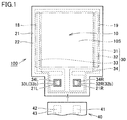
- Fig. 1 is a plan view showing planar light-emitting module 100
- Fig. 2 is a plan view showing planar light-emitting module 100 in an exploded state
- Fig. 3 is a plan view showing planar light-emitting module 100 in a further exploded state
- Fig. 4 is a cross-sectional view taken along the line IV-IV in Fig. 3
- Fig. 5 is a plan view for explaining the operation and effects of planar light-emitting module 100.
- Planar light-emitting module 100 is connected with, for example, external wiring 40 (see Fig. 1 ), and planar light-emitting module 100 can be used in various applications such as lighting, decoration, and backlights.
- External wiring 40 is formed of, for example, FPC and includes contact portions 41, 42 and a substrate 43 for holding them. As will be detailed later, contact portions 41, 42 are connected to feeding portions 32R, 33L (exposed portion), respectively, of planar light-emitting module 100 through not-shown conductive adhesive (ACF).
- ACF conductive adhesive
- Planar light-emitting module 100 is configured such that a planar light-emitting element 10 is sandwiched between and sealed by a pair of sealing sheets 21, 22 ( Fig. 1 , Fig. 2 ) from above and below.
- Fig. 2 shows planar light-emitting element 10 using a dashed and double-dotted line
- Fig. 3 does not show sealing sheet 21.
- planar light-emitting module 100 includes planar light-emitting element 10, a pair of sealing sheet 21 (first sealing sheet) and sealing sheet 22 (second sealing sheet) holding planar light-emitting element 10 from above and below, and a wiring member 30 electrically connected to planar light-emitting element 10 for feeding planar light-emitting element 10. They will be described one by one below.
- planar light-emitting element 10 is formed of organic EL and disposed between sealing sheet 21 and sealing sheet 22.
- Planar light-emitting element 10 is disposed such that a front surface 10S (light-emitting surface) is positioned on the side on which sealing sheet 21 is disposed (the front side of the drawing sheet of Fig. 2 ).
- the thickness of planar light-emitting element 10 is, for example, 50 ⁇ m to 200 ⁇ m. It is preferable that planar light-emitting element 10 has flexibility.
- Planar light-emitting element 10 in the present embodiment has a rectangular shape in a two-dimensional view (see Fig. 3 ).
- planar light-emitting element 10 includes a transparent substrate 11, a barrier layer 12, an anode 13, an emissive layer 14, a cathode 15, a sealing member 16, and an insulating layer 17.
- Transparent substrate 11, barrier layer 12, anode 13, emissive layer 14, cathode 15, and sealing member 16 are stacked in order from the front surface 10S (light-emitting surface) side of planar light-emitting element 10 toward the back surface side of planar light-emitting element 10.
- Transparent substrate 11 is formed of glass, thin film glass, resin film, or the like.
- Transparent substrate 11 is a member that forms front surface 10S of planar light-emitting element 10 and has a rectangular shape in a two-dimensional view.
- Barrier layer 12 has transparency and is formed to cover the whole of the surface of transparent substrate 11.
- Barrier layer 12 is formed of, for example, a silicon compound such as silicon oxide and silicon nitride or a metal compound such as metal oxide and metal nitride, or a mixture thereof.
- Anode 13 is a conductive film having transparency and is formed by depositing ITO or the like on barrier layer 12.
- An ITO film for forming anode 13 is divided into two regions by patterning to form a feeding portion 18 (for anode) and a feeding portion 19 (for cathode).
- the ITO film that forms feeding portion 19 is connected to cathode 15.
- emissive layer 14 When supplied power, emissive layer 14 produces light by the action of field effect. Emissive layer 14 is formed with a single layer or a plurality of stacked layers.
- Cathode 15 is, for example, aluminum (Al) and is formed to cover emissive layer 14. Insulating layer 17 is provided between cathode 15 and anode 13. A portion of cathode 15 that is opposite to the side on which insulating layer 17 ( Fig. 3 ) is located is connected to the ITO film that forms feeding portion 19.
- Sealing member 16 is formed of glass, thin film glass, resin film, or the like. Sealing member 16 seals almost the whole of anode 13, emissive layer 14, and cathode 15 on transparent substrate 11 (on barrier layer 12). Part of the ITO film formed on barrier layer 12 is exposed from sealing member 16 to form feeding portions 18, 19 (portions where electrical connection is made). Feeding portions 18, 19 are located on the outside of sealing member 16 and located opposite to each other with respect to sealing member 16 (emissive layer 14).
- planar light-emitting element 10 configured as described above, power is fed through wiring member 30 (which will be detailed later), feeding portions 18. 19, anode 13. and cathode 15 to emissive layer 14. Light is produced in emissive layer 14. and the light passes through anode 13, barrier layer 12, and transparent substrate 11 and is extracted from front surface 10S of planar light-emitting element 10.
- sealing sheet 21 and sealing sheet 22 are bonded to each other to seal planar light-emitting element 10 in the inside thereof.
- a resin member having a sheet shape or a film shape is used as sealing sheets 21, 22. It is preferable that sealing sheets 21, 22 have flexibility.
- the thickness of sealing sheets 21, 22 is, for example, 25 ⁇ m to 50 ⁇ m.
- sealing sheets 21, 22 examples include polyethylene terephthalate, polypropylene, acrylic, polyimide, and polysulfone. In addition to these materials, a variety of films deposited for improving the barrier characteristic may be used for sealing sheets 21, 22.
- the color of sealing sheets 21, 22 is not limited, and at least sealing sheet 21 of sealing sheets 21. 22 has high transparency to allow light emitted from front surface 10S of planar light-emitting element 10 to pass through. Sealing sheet 22 may also have transparency.
- Adhesive (not shown) is provided on the inside surfaces of sealing sheets 21, 22 to bond sealing sheets 21, 22.
- a variety of materials such as thermoplastic resin, thermosetting resin, and UV curable resin can be used as adhesive.
- the thickness of adhesive is, for example, 20 ⁇ m to 50 ⁇ m.
- sealing sheets 21. 22 have a rectangular portion larger than the area of planar light-emitting element 10.
- Wiring member 30 described later (substrate 31, electrodes 32, 33, and protective film 34) is disposed on the rectangular portion of sealing sheet 22.
- Planar light-emitting element 10 is placed on wiring member 30 (protective film 34) such that sealing member 16 of planar light-emitting element 10 (see Fig. 4 ) overlaps protective film 34 of wiring member 30.
- Wiring member 30 includes electrodes 32, 33, and electrodes 32, 33 (linear portions 32a, 33a) are electrically connected to feeding portions 19, 18 of planar light-emitting element 10, respectively.
- sealing sheet 21 has a pair of openings 21L, 21R ( Fig. 2 ).
- the position of opening 21L corresponds to the position of feeding portion 33L of wiring member 30 and the position of aperture 34L provided in protective film 34 of wiring member 30 (see Fig. 1 ).
- feeding portion 33L is located on the inside of aperture 34L
- feeding portion 33L and aperture 34L are located on the inside of opening 21L when feeding portion 33L.
- aperture 34L, and opening 21L are viewed from the direction parallel to the direction in which planar light-emitting element 10, wiring member 30, and sealing sheets 21, 22 arc superimposed on each other (when viewed two-dimcnsionally).
- the position of opening 21R corresponds to the position of feeding portion 32R of wiring member 30 and the position of aperture 34R provided in protective film 34 of wiring member 30. Specifically, when planar light-emitting element 10 and wiring member 30 are sandwiched and sealed between a pair of sealing sheets 21, 22 from above and below, feeding portion 32R is located on the inside of aperture 34R, and feeding portion 32R and aperture 34R are located on the inside of opening 21R when feeding portion 32R, aperture 34R, and opening 21R are viewed from the direction parallel to the direction in which planar light-emitting element 10, wiring member 30, and sealing sheets 21, 22 are superimposed on each other (when viewed two-dimensionally). Further detail of openings 21L, 21R will be described later.
- wiring member 30 is electrically connected to planar light-emitting element 10 and is disposed between sealing sheets 21 and 22.
- wiring member 30 includes a substrate 31, electrodes 32, 33, and a protective film 34. It is preferable that wiring member 30 has flexibility as a whole.
- Substrate 31 and protective film 34 coverlay
- Protective film 34 has a pair of apertures 34L, 34R.
- Protective film 34 is provided so as to cover at least the portions located around feeding portions 32R, 33L (exposed portions) in electrodes 32, 33 and serves to protect electrodes 32, 33 and improve the sealing performance for the electrodes.
- Electrodes 32, 33 are formed on substrate 31 by a deposition technique such as printing, vapor deposition, plating and sputtering.
- the thickness of electrodes 32, 33 is, for example, 0.1 ⁇ m to 10 ⁇ m.
- the material of electrodes 32, 33 is, for example, copper or nickel, or a laminate thereof. In addition to copper or nickel, or a laminate thereof, the surface thereof may be plated with gold.
- Electrodes 32, 33 may not be deposited but may be formed by affixing a metal thin foil such as copper foil tape on the surface of substrate 31 using conductive adhesive (for example, ACF: anisotropic conductive film).
- Electrode 32 includes a linear portion 32a extending longitudinally to match with the position and shape of feeding portion 19 of planar light-emitting element 10, a rectangular portion 32b having feeding portion 32R (exposed portion) inside thereof, and a connecting portion 32c connecting linear portion 32a with rectangular portion 32b.
- protective film 34 is disposed on substrate 31 and electrodes 32. 33, linear portion 32a is not covered with protective film 34.
- Feeding portion 19 of planar light-emitting element 10 is electrically connected to linear portion 32a of electrode 32 through not-shown conductive adhesive (ACF).
- Feeding portion 19 of planar light-emitting element 10 may be pressure-welded to linear portion 32a of electrode 32 without using conductive adhesive (ACF).
- Feeding portion 32R is a portion of electrode 32 that is exposable through aperture 34R when protective film 34 is disposed on substrate 31 and electrode 32. That is, feeding portion 32R (exposed portion) is a portion that is disposed to be exposable on the outside through aperture 34R and opening 21R and connected to contact portion 41 of external wiring 40 ( Fig. 1 ) when protective film 34, planar light-emitting element 10, and sealing sheet 21 are disposed in order on electrode 32.
- exposuresable is a concept that includes not only the state in which feeding portion 32R is actually exposed through aperture 34R and opening 21R but also the state in which feeding portion 32R in that state is further covered with another sealing member or conductive paste as necessary and not exposed.
- the position of aperture 34R provided in protective film 34 corresponds to the position of feeding portion 32R of wiring member 30 (electrode 32) and the position of opening 21R provided in sealing sheet 21 (see Fig. 1 ).
- the size of aperture 34R is smaller than the size of opening 21R (the aperture area is smaller).
- the size of opening 21R is smaller than the size of rectangular portion 32b of electrode 32. Therefore, in the state in which protective film 34, planar light-emitting element 10, and sealing sheet 21 are disposed in order on electrode 32, the edge portion that forms opening 21R in sealing sheet 21 is located outside the position of aperture 34R and located on a portion having a flat shape in the surface of protective film 34 (located on rectangular portion 32b with protective film 34 interposed).
- Protective film 34 (specifically, the portion around aperture 34R in protective film 34) is disposed on the surface of the portion located around feeding portion 32R in rectangular portion 32b ( Fig. 3 ).
- the portion around aperture 34R in protective film 34 is bonded to sealing sheet 21 through adhesive (see Fig. 2 ). If the bonding force between protective film 34 and sealing sheet 21 is high, the sealing performance of planar light-emitting module 100 can be improved. Therefore, it is preferable that the portion located around feeding portion 32R in rectangular portion 32b has a surface shape that has little or no step and is as flat as possible (with highest possible flatness).
- Electrode 33 includes a linear portion 33a extending longitudinally so as to match with the position and shape of feeding portion 18 of planar light-emitting element 10, a rectangular portion 33b having a feeding portion 33L (exposed portion) inside thereof, and a connecting portion 33c connecting linear portion 33a with rectangular portion 33b.
- linear portion 33a is not covered with protective film 34.
- Feeding portion 18 of planar light-emitting element 10 is electrically connected to linear portion 33a of electrode 33 through not-shown conductive adhesive (ACF).
- Feeding portion 18 of planar light-emitting element 10 may be pressure-welded to linear portion 33a of electrode 33 without using conductive adhesive (ACF).
- Feeding portion 33L is a portion of electrode 33 that is exposable through aperture 34L when protective film 34 is disposed on substrate 31 and electrode 33. That is, feeding portion 33L (exposed portion) is a portion that is disposed so as to be exposable on the outside through aperture 34L and opening 21L and connected to contact portion 42 of external wiring 40 ( Fig. 1 ) when protective film 34, planar light-emitting element 10. and sealing sheet 21 are disposed in order on electrode 33.
- exposuresable is a concept that includes not only the state in which feeding portion 33L is actually exposed through aperture 34L and opening 21L but also the state in which feeding portion 33L in that state is further covered with another sealing member or conductive paste as necessary and not exposed.
- the position of aperture 34L provided in protective film 34 corresponds to the position of feeding portion 33L of wiring member 30 (electrode 33) and the position of opening 21L provided in sealing sheet 21 (see Fig. 1 ).
- the size of aperture 34L is smaller than the size of opening 21L (the aperture area is smaller).
- the size of opening 21L is smaller than the size of rectangular portion 33b of electrode 33. Therefore, in the state in which protective film 34, planar light-emitting element 10, and sealing sheet 21 are disposed in order on electrode 33, the edge portion that forms opening 21L in sealing sheet 21 is located outside aperture 34L and is located on a portion having a flat shape in the surface of protective film 34 (located on rectangular portion 33b with protective film 34 interposed).
- Protective film 34 (specifically, the portion around aperture 34L in protective film 34) is disposed on the surface of the portion located around feeding portion 33L in rectangular portion 33b ( Fig. 3 ).
- the portion around aperture 34L in protective film 34 is bonded to sealing sheet 21 through adhesive (see Fig. 2 ). If the bonding force between protective film 34 and sealing sheet 21 is high, the sealing performance of planar light-emitting module 100 can be improved. Therefore, it is preferable that the portion located around feeding portion 33L in rectangular portion 33b has a surface shape that has little or no step and is as flat as possible (with highest possible flatness).
- electrode 32 and electrode 33 of wiring member 30 extend on the same side of planar light-emitting element 10, and feeding portions 32R, 33L (rectangular portions 32b, 33b) are disposed to be adjacent to each other.
- feeding portions 33L, 32R of electrodes 33, 32 are exposed through apertures 34L, 34R provided in protective film 34 and openings 21L, 21R provided in sealing sheet 21 (first sealing sheet), respectively.
- Contact portions 42, 41 of external wiring 40 can be electrically connected to feeding portions 33L. 32R, respectively.
- External wiring 40 is not positioned between the end portions of sealing sheets 21, 22.
- Region RA shown by a hatching in Fig. 5 is located around planar light-emitting element 10, around substrate 31, or around protective film 34.
- This region RA indicates a portion where it is more likely than other portions that the thickness of planar light-emitting element 10, the thickness of electrodes 32, 33, and the thickness of protective film 34 produce steps when sealing sheets 21, 22 are bonded, and the presence of the steps results in a gap. If this region RA reaches outer edge EE ( Fig. 5 ) or openings 21L, 21R of sealing sheets 21, 22, moisture or other substances easily intrude through the portion where region RA reaches. Planar light-emitting module 100 in the present embodiment, however, is not configured as such.
- sealing sheet 21 when sealing sheet 21 is bonded to sealing sheet 22, the portions around apertures 34L, 34R in protective film 34 are bonded to sealing sheet 21 through adhesive (see Fig. 2 ).
- the edge portion that forms opening 21L in sealing sheet 21 is located outside the position of aperture 34L and located on a portion having a flat shape in the surface of protective film 34 (located on rectangular portion 33b with protective film 34 interposed).
- the edge portion that forms opening 21R in sealing sheet 21 is located outside the position of aperture 34R and located on a portion having a flat shape in the surface of protective film 34 (located on rectangular portion 32b with protective film 34 interposed). Since a sealing structure that contains region RA in the inside by bonding between flat surfaces is thus achieved, it can be said that reduction of sealing performance is suppressed compared with the conventional sealing structure.
- planar light-emitting module 100 does not employ a configuration having a conductor (electrode pin) inserted (pierced) into the scaling sheet. Compared with the case of PTD 2, the possibility that the scaling sheet is broken is low, and reliable sealing performance can be kept for a long time compared with the case of PTD 2.
- Planar light-emitting module 101 differs from planar light-emitting module 100 of the first embodiment in that one opening 21H is provided in sealing sheet 21.
- the edge portion that forms opening 21H in sealing sheet 21 is located outside apertures 34L, 34R provided in protective film 34 ( Fig. 6 ). However, the edge portion that forms opening 21H in sealing sheet 21 is not located on a portion having a flat shape in the surface of protective film 34. Steps 32d, 33d ( Fig. 6 ) are formed on protective film 34 due the presence of electrodes 32, 33 (rectangular portions 32b, 33b). The edge portion that forms opening 21H in sealing sheet 21 is disposed to extend across steps 32d, 33d (disposed to cross steps 32d, 33d) and is not located on a portion having a flat shape in the surface of protective film 34.
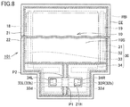
- Region RB shown by a hatching in Fig. 8 is located around planar light-emitting element 10, around substrate 31, or around protective film 34.
- region RB reaches opening 21H (see the portions surrounded by circles PI, P2), and moisture or other substances easily intrude through the portion where region RB reaches.
- planar light-emitting element 10 is sealed by sealing sheets 21, 22, bonding of flat surfaces fails to be achieved, and sufficient sealing performance fails to be obtained.
- Planar light-emitting module 102 includes a wiring member 30A instead of wiring member 30 (the first embodiment).
- Wiring member 30A differs from wiring member 30 in that it does not include protective film 34.
- Feeding portion 32R in planar light-emitting module 102 is a portion of electrode 32 that is exposable through opening 21R when sealing sheet 21 is disposed on planar light-emitting element 10, substrate 31, and electrode 32.
- the size of opening 21R is smaller than the size of rectangular portion 32b of electrode 32.
- feeding portion 32R is located on the inside of opening 21R when opening 21R and feeding portion 32R are viewed from the direction parallel to the direction in which planar light-emitting element 10 and sealing sheets 21. 22 are superimposed on each other (when viewed two-dimensionally).
- sealing sheet 21 In the state in which sealing sheet 21 is disposed on electrode 32, the edge portion that forms opening 21R in sealing sheet 21 is located on a portion having a flat shape in the surface of rectangular portion 32b of electrode 32.
- the portion around feeding portion 32R in electrode 32 (rectangular portion 32b) is bonded to sealing sheet 21 through adhesive. It is preferable that he portion located around feeding portion 32R in rectangular portion 32b has a surface shape that has little or no step and is as flat as possible (with highest possible flatness).
- Feeding portion 33L in planar light-emitting module 102 is a portion of electrode 33 that is exposable through opening 21L when sealing sheet 21 is disposed on planar light-emitting element 10, substrate 31, and electrode 33.
- the size of opening 21L is smaller than the size of rectangular portion 33b of electrode 33.
- the edge portion that forms opening 21L in sealing sheet 21 is located on a portion having a flat shape in the surface of rectangular portion 33b of electrode 32.
- the portion around feeding portion 33L in electrode 33 (rectangular portion 33b) is bonded to sealing sheet 21 through adhesive. It is preferable that the portion located around feeding portion 33L in rectangular portion 33b has a surface shape that has little or no step and is as flat as possible (with highest possible flatness).
- feeding portions 33L. 32R of electrodes 33, 32 are exposed through openings 21L, 21R, respectively, provided in sealing sheet 21 (first sealing sheet).
- Contact portions 42, 41 of external wiring 40 ( Fig. 1 ) can be electrically connected to feeding portions 33L, 32R, respectively.
- External wiring 40 is not located between the end portions of sealing sheets 21, 22.
- the end portions of sealing sheets 21, 22 can be bonded to each other appropriately, and sealing performance by sealing sheets 21, 22 can be obtained.
- Region RA shown by a hatching in Fig. 11 is located around planar light-emitting element 10, around substrate 31, or around protective film 34. Region RA does not reach the outer edge EE ( Fig. 11 ) of sealing sheets 21, 22 or openings 21L, 21R.
- a sealing structure that contains region RA in the inside by bonding between flat surfaces can be achieved, and therefore it can be said that reduction of sealing performance is suppressed.
- Planar light-emitting module 102 does not have a configuration having a conductor (electrode pin) inserted (pierced) into the sealing sheet. Reliable sealing performance can be kept for a long time compared with the case of PTD 2.
- the planar light-emitting module based on an aspect includes a first sealing sheet having an opening, a second sealing sheet bonded to the first sealing sheet, a planar light-emitting element disposed between the first sealing sheet and the second sealing sheet and sealed by the first sealing sheet and the second sealing sheet, and a wiring member disposed between the first sealing sheet and the second sealing sheet and electrically connected to the planar light-emitting element.
- the wiring member includes a substrate, an electrode formed on the substrate and having an exposed portion disposed so as to be exposable from the opening of the first sealing sheet, and a protective film having an aperture corresponding to the exposed portion and provided so as to cover at least the periphery of the exposed portion of the electrode.
- One exposed portion described above is exposable through one opening and one aperture described above.
- An edge portion that forms the opening in the first sealing sheet is located outside the aperture and is located on a portion having a flat shape in a surface of the protective film.
- a planar light-emitting module includes a first sealing sheet having an opening, a second sealing sheet bonded to the first sealing sheet, a planar light-emitting element disposed between the first sealing sheet and the second sealing sheet and sealed by the first sealing sheet and the second sealing sheet, and a wiring member disposed between the first sealing sheet and the second sealing sheet and electrically connected to the planar light-emitting element.
- the wiring member includes a substrate and an electrode formed on the substrate and having an exposed portion disposed so as to be exposable from the opening of the first sealing sheet. One exposed portion described above is exposable through one opening described above. An edge portion that forms the opening in the first scaling sheet is located on a portion having a flat shape in the surface of the electrode.
- the first sealing sheet, the second sealing sheet, the planar light-emitting element, and the wiring member have flexibility.
- the portion that forms the opening in the first sealing sheet is bonded to a portion having a flat surface shape (in other words, a portion where steps are not formed). Since a sealing structure can be achieved by bonding between flat surfaces, the configuration above can suppress reduction of sealing performance compared with the conventional sealing structures.
Landscapes
- Engineering & Computer Science (AREA)
- General Engineering & Computer Science (AREA)
- Physics & Mathematics (AREA)
- Optics & Photonics (AREA)
- Microelectronics & Electronic Packaging (AREA)
- Electroluminescent Light Sources (AREA)
- Non-Portable Lighting Devices Or Systems Thereof (AREA)
- Planar Illumination Modules (AREA)
- Arrangement Of Elements, Cooling, Sealing, Or The Like Of Lighting Devices (AREA)
Abstract
Description
- The present invention relates to a planar light-emitting module including a sheet for sealing a planar light-emitting element.
- A planar light-emitting element is formed with a thin planar light source such as organic EL. Planar light-emitting modules including planar light-emitting elements are installed both indoors and outdoors and utilized in a wide variety of applications such as signage, signs, backlights, lighting, and illumination. The planar light-emitting elements require protection from dust, ultraviolet rays, and weather. In general, the planar light-emitting element is disposed between a pair of sheets and sealed so as to be sandwiched between the pair of sheets (for example, see
PTDs 1, 2 below). - In the organic EL device disclosed in PTD 1 (Japanese Laid-Open Patent Publication No.
2010-244698 - In the electroluminescence light disclosed in Japanese Laid-Open Patent Publication No.
H01-117295 PTD 2, high sealing performance can be achieved because the entire planar light-emitting element and the entire electrode lead terminals can be sealed without exposing the electrode lead terminals on the outside. -
- PTD 1: Japanese Laid-Open Patent Publication No.
2010-244698 - PTD 2: Japanese Laid-Open Patent Publication No.
H01-117295 - When the configuration disclosed in PTD 1 (Japanese Laid-Open Patent Publication No.
2010-244698 - When the configuration disclosed in Japanese Laid-Open Patent Publication No.
H01-117295 - The present invention is made in view of the foregoing situation and is aimed to provide a planar light-emitting module having a configuration that can suppress reduction of sealing performance due to the presence of a wiring member.
- A planar light-emitting module based on an aspect of the present invention includes a first sealing sheet having an opening, a second sealing sheet bonded to the first sealing sheet, a planar light-emitting element disposed between the first sealing sheet and the second sealing sheet and sealed by the first sealing sheet and the second sealing sheet, and a wiring member disposed between the first sealing sheet and the second sealing sheet and electrically connected to the planar light-emitting element. The wiring member includes a substrate, an electrode formed on the substrate and having an exposed portion disposed so as to be exposable from the opening of the first sealing sheet, and a protective film having an aperture corresponding to the exposed portion and provided so as to cover at least periphery of the exposed portion of the electrode. One exposed portion described above is exposable through one opening and one aperture described above. An edge portion that forms the opening in the first sealing sheet is located outside the aperture and located on a portion having a flat shape in a surface of the protective film.
- A planar light-emitting module based on another aspect of the present invention includes a first sealing sheet having an opening, a second sealing sheet bonded to the first sealing sheet, a planar light-emitting element disposed between the first sealing sheet and the second sealing sheet and sealed by the first sealing sheet and the second sealing sheet, and a wiring member disposed between the first sealing sheet and the second sealing sheet and electrically connected to the planar light-emitting element. The wiring member includes a substrate and an electrode formed on the substrate and having an exposed portion disposed so as to be exposable from the opening of the first sealing sheet. One exposed portion described above is exposable through one opening described above. An edge portion that forms the opening in the first sealing sheet is located on a portion having a flat shape in a surface of the electrode.
-
-
Fig. 1 is a plan view showing a planar light-emitting module in a first embodiment. -
Fig. 2 is a plan view showing the planar light-emitting module in the first embodiment in an exploded state. -
Fig. 3 is a plan view showing the planar light-emitting module in the first embodiment in a further exploded state. -
Fig. 4 is a cross-sectional view taken along the line IV-IV inFig. 3 . -
Fig. 5 is a plan view for explaining the operation and effects of the planar light-emitting module in the first embodiment. -
Fig. 6 is a plan view showing a planar light-emitting module in a comparative example. -
Fig. 7 is a plan view showing the planar light-emitting module in the comparative example in an exploded state. -
Fig. 8 is a plan view for explaining the operation and effects of the planar light-emitting module in the comparative example. -
Fig. 9 is a plan view showing a planar light-emitting module in a second embodiment. -
Fig. 10 is a plan view showing the planar light-emitting module in the second embodiment in an exploded state. -
Fig. 11 is a plan view for explaining the operation and effects of the planar light-emitting module in the second embodiment. - Embodiments will be described below with reference to the drawings. The same parts and corresponding parts are denoted with the same reference numerals and an overlapping description may not be repeated.
- Referring to
Fig. 1 to Fig. 5 , a planar light-emitting module 100 in a first embodiment will be described.Fig. 1 is a plan view showing planar light-emitting module 100,Fig. 2 is a plan view showing planar light-emitting module 100 in an exploded state,Fig. 3 is a plan view showing planar light-emitting module 100 in a further exploded state, andFig. 4 is a cross-sectional view taken along the line IV-IV inFig. 3 .Fig. 5 is a plan view for explaining the operation and effects of planar light-emitting module 100. - Planar light-
emitting module 100 is connected with, for example, external wiring 40 (seeFig. 1 ), and planar light-emitting module 100 can be used in various applications such as lighting, decoration, and backlights.External wiring 40 is formed of, for example, FPC and includescontact portions substrate 43 for holding them. As will be detailed later,contact portions portions emitting module 100 through not-shown conductive adhesive (ACF). - Planar light-
emitting module 100 is configured such that a planar light-emittingelement 10 is sandwiched between and sealed by a pair ofsealing sheets 21, 22 (Fig. 1 ,Fig. 2 ) from above and below. For the sake of convenience,Fig. 2 shows planar light-emittingelement 10 using a dashed and double-dotted line, andFig. 3 does not showsealing sheet 21. More specifically, planar light-emitting module 100 includes planar light-emitting element 10, a pair of sealing sheet 21 (first sealing sheet) and sealing sheet 22 (second sealing sheet) holding planar light-emitting element 10 from above and below, and awiring member 30 electrically connected to planar light-emittingelement 10 for feeding planar light-emitting element 10. They will be described one by one below. - As shown in
Fig. 1 to Fig. 4 (mainlyFig. 3 andFig. 4 ), planar light-emittingelement 10 is formed of organic EL and disposed between sealingsheet 21 andsealing sheet 22. Planar light-emitting element 10 is disposed such that afront surface 10S (light-emitting surface) is positioned on the side on whichsealing sheet 21 is disposed (the front side of the drawing sheet ofFig. 2 ). The thickness of planar light-emittingelement 10 is, for example, 50 µm to 200 µm. It is preferable that planar light-emittingelement 10 has flexibility. Planar light-emittingelement 10 in the present embodiment has a rectangular shape in a two-dimensional view (seeFig. 3 ). - As shown in
Fig. 4 . planar light-emittingelement 10 includes atransparent substrate 11, abarrier layer 12, ananode 13, anemissive layer 14, acathode 15, a sealingmember 16, and an insulatinglayer 17.Transparent substrate 11,barrier layer 12,anode 13,emissive layer 14,cathode 15, and sealingmember 16 are stacked in order from thefront surface 10S (light-emitting surface) side of planar light-emittingelement 10 toward the back surface side of planar light-emittingelement 10. -
Transparent substrate 11 is formed of glass, thin film glass, resin film, or the like.Transparent substrate 11 is a member that formsfront surface 10S of planar light-emittingelement 10 and has a rectangular shape in a two-dimensional view.Barrier layer 12 has transparency and is formed to cover the whole of the surface oftransparent substrate 11.Barrier layer 12 is formed of, for example, a silicon compound such as silicon oxide and silicon nitride or a metal compound such as metal oxide and metal nitride, or a mixture thereof. -
Anode 13 is a conductive film having transparency and is formed by depositing ITO or the like onbarrier layer 12. An ITO film for forminganode 13 is divided into two regions by patterning to form a feeding portion 18 (for anode) and a feeding portion 19 (for cathode). The ITO film that forms feedingportion 19 is connected tocathode 15. - When supplied power,
emissive layer 14 produces light by the action of field effect.Emissive layer 14 is formed with a single layer or a plurality of stacked layers.Cathode 15 is, for example, aluminum (Al) and is formed to coveremissive layer 14. Insulatinglayer 17 is provided betweencathode 15 andanode 13. A portion ofcathode 15 that is opposite to the side on which insulating layer 17 (Fig. 3 ) is located is connected to the ITO film that forms feedingportion 19. - Sealing
member 16 is formed of glass, thin film glass, resin film, or the like. Sealingmember 16 seals almost the whole ofanode 13,emissive layer 14, andcathode 15 on transparent substrate 11 (on barrier layer 12). Part of the ITO film formed onbarrier layer 12 is exposed from sealingmember 16 to form feedingportions 18, 19 (portions where electrical connection is made). Feedingportions member 16 and located opposite to each other with respect to sealing member 16 (emissive layer 14). - In planar light-emitting
element 10 configured as described above, power is fed through wiring member 30 (which will be detailed later), feedingportions 18. 19,anode 13. andcathode 15 toemissive layer 14. Light is produced inemissive layer 14. and the light passes throughanode 13,barrier layer 12, andtransparent substrate 11 and is extracted fromfront surface 10S of planar light-emittingelement 10. - Referring to
Fig. 1 to Fig. 3 , a pair of sealingsheet 21 and sealingsheet 22 are bonded to each other to seal planar light-emittingelement 10 in the inside thereof. For example, a resin member having a sheet shape or a film shape is used as sealingsheets sheets sheets - Examples of the specific material of sealing
sheets sheets sheets sheet 21 of sealingsheets 21. 22 has high transparency to allow light emitted fromfront surface 10S of planar light-emittingelement 10 to pass through. Sealingsheet 22 may also have transparency. - Adhesive (not shown) is provided on the inside surfaces of sealing
sheets bond sealing sheets - As shown in
Fig. 2 , sealingsheets 21. 22 have a rectangular portion larger than the area of planar light-emittingelement 10. Wiringmember 30 described later (substrate 31,electrodes sheet 22. Planar light-emittingelement 10 is placed on wiring member 30 (protective film 34) such that sealingmember 16 of planar light-emitting element 10 (seeFig. 4 ) overlapsprotective film 34 ofwiring member 30. Wiringmember 30 includeselectrodes electrodes 32, 33 (linear portions portions element 10, respectively. - As shown in
Fig. 1 andFig. 2 , sealingsheet 21 has a pair ofopenings Fig. 2 ). The position of opening 21L corresponds to the position of feedingportion 33L of wiringmember 30 and the position ofaperture 34L provided inprotective film 34 of wiring member 30 (seeFig. 1 ). Specifically, when planar light-emittingelement 10 andwiring member 30 are sandwiched and sealed between a pair of sealingsheets portion 33L is located on the inside ofaperture 34L, and feedingportion 33L andaperture 34L are located on the inside ofopening 21L when feedingportion 33L.aperture 34L, andopening 21L are viewed from the direction parallel to the direction in which planar light-emittingelement 10,wiring member 30, and sealingsheets - The position of opening 21R corresponds to the position of feeding
portion 32R of wiringmember 30 and the position ofaperture 34R provided inprotective film 34 ofwiring member 30. Specifically, when planar light-emittingelement 10 andwiring member 30 are sandwiched and sealed between a pair of sealingsheets portion 32R is located on the inside ofaperture 34R, and feedingportion 32R andaperture 34R are located on the inside ofopening 21R when feedingportion 32R,aperture 34R, andopening 21R are viewed from the direction parallel to the direction in which planar light-emittingelement 10,wiring member 30, and sealingsheets openings - Referring to
Fig. 3 ,wiring member 30 is electrically connected to planar light-emittingelement 10 and is disposed between sealingsheets wiring member 30 includes asubstrate 31,electrodes protective film 34. It is preferable that wiringmember 30 has flexibility as a whole.Substrate 31 and protective film 34 (coverlay) have an outer shape smaller than sealingsheets Protective film 34 has a pair ofapertures Protective film 34 is provided so as to cover at least the portions located around feedingportions electrodes electrodes -
Electrodes substrate 31 by a deposition technique such as printing, vapor deposition, plating and sputtering. The thickness ofelectrodes electrodes Electrodes substrate 31 using conductive adhesive (for example, ACF: anisotropic conductive film). -
Electrode 32 includes alinear portion 32a extending longitudinally to match with the position and shape of feedingportion 19 of planar light-emittingelement 10, arectangular portion 32b havingfeeding portion 32R (exposed portion) inside thereof, and a connectingportion 32c connectinglinear portion 32a withrectangular portion 32b. Whenprotective film 34 is disposed onsubstrate 31 andelectrodes 32. 33,linear portion 32a is not covered withprotective film 34. Feedingportion 19 of planar light-emittingelement 10 is electrically connected tolinear portion 32a ofelectrode 32 through not-shown conductive adhesive (ACF). Feedingportion 19 of planar light-emittingelement 10 may be pressure-welded tolinear portion 32a ofelectrode 32 without using conductive adhesive (ACF). - Feeding
portion 32R is a portion ofelectrode 32 that is exposable throughaperture 34R whenprotective film 34 is disposed onsubstrate 31 andelectrode 32. That is, feedingportion 32R (exposed portion) is a portion that is disposed to be exposable on the outside throughaperture 34R andopening 21R and connected to contactportion 41 of external wiring 40 (Fig. 1 ) whenprotective film 34, planar light-emittingelement 10, and sealingsheet 21 are disposed in order onelectrode 32. As used herein "exposable" is a concept that includes not only the state in whichfeeding portion 32R is actually exposed throughaperture 34R andopening 21R but also the state in whichfeeding portion 32R in that state is further covered with another sealing member or conductive paste as necessary and not exposed. - The position of
aperture 34R provided inprotective film 34 corresponds to the position of feedingportion 32R of wiring member 30 (electrode 32) and the position ofopening 21R provided in sealing sheet 21 (seeFig. 1 ). The size ofaperture 34R is smaller than the size ofopening 21R (the aperture area is smaller). The size ofopening 21R is smaller than the size ofrectangular portion 32b ofelectrode 32. Therefore, in the state in whichprotective film 34, planar light-emittingelement 10, and sealingsheet 21 are disposed in order onelectrode 32, the edge portion that forms opening 21R in sealingsheet 21 is located outside the position ofaperture 34R and located on a portion having a flat shape in the surface of protective film 34 (located onrectangular portion 32b withprotective film 34 interposed). - Protective film 34 (specifically, the portion around
aperture 34R in protective film 34) is disposed on the surface of the portion located around feedingportion 32R inrectangular portion 32b (Fig. 3 ). The portion aroundaperture 34R inprotective film 34 is bonded to sealingsheet 21 through adhesive (seeFig. 2 ). If the bonding force betweenprotective film 34 and sealingsheet 21 is high, the sealing performance of planar light-emittingmodule 100 can be improved. Therefore, it is preferable that the portion located around feedingportion 32R inrectangular portion 32b has a surface shape that has little or no step and is as flat as possible (with highest possible flatness). -
Electrode 33 includes alinear portion 33a extending longitudinally so as to match with the position and shape of feedingportion 18 of planar light-emittingelement 10, arectangular portion 33b having a feedingportion 33L (exposed portion) inside thereof, and a connecting portion 33c connectinglinear portion 33a withrectangular portion 33b. Whenprotective film 34 is disposed onsubstrate 31 andelectrodes linear portion 33a is not covered withprotective film 34. Feedingportion 18 of planar light-emittingelement 10 is electrically connected tolinear portion 33a ofelectrode 33 through not-shown conductive adhesive (ACF). Feedingportion 18 of planar light-emittingelement 10 may be pressure-welded tolinear portion 33a ofelectrode 33 without using conductive adhesive (ACF). - Feeding
portion 33L is a portion ofelectrode 33 that is exposable throughaperture 34L whenprotective film 34 is disposed onsubstrate 31 andelectrode 33. That is, feedingportion 33L (exposed portion) is a portion that is disposed so as to be exposable on the outside throughaperture 34L andopening 21L and connected to contactportion 42 of external wiring 40 (Fig. 1 ) whenprotective film 34, planar light-emittingelement 10. and sealingsheet 21 are disposed in order onelectrode 33. As used herein "exposable" is a concept that includes not only the state in whichfeeding portion 33L is actually exposed throughaperture 34L andopening 21L but also the state in whichfeeding portion 33L in that state is further covered with another sealing member or conductive paste as necessary and not exposed. - The position of
aperture 34L provided inprotective film 34 corresponds to the position of feedingportion 33L of wiring member 30 (electrode 33) and the position ofopening 21L provided in sealing sheet 21 (seeFig. 1 ). The size ofaperture 34L is smaller than the size ofopening 21L (the aperture area is smaller). The size ofopening 21L is smaller than the size ofrectangular portion 33b ofelectrode 33. Therefore, in the state in whichprotective film 34, planar light-emittingelement 10, and sealingsheet 21 are disposed in order onelectrode 33, the edge portion that forms opening 21L in sealingsheet 21 is located outsideaperture 34L and is located on a portion having a flat shape in the surface of protective film 34 (located onrectangular portion 33b withprotective film 34 interposed). - Protective film 34 (specifically, the portion around
aperture 34L in protective film 34) is disposed on the surface of the portion located around feedingportion 33L inrectangular portion 33b (Fig. 3 ). The portion aroundaperture 34L inprotective film 34 is bonded to sealingsheet 21 through adhesive (seeFig. 2 ). If the bonding force betweenprotective film 34 and sealingsheet 21 is high, the sealing performance of planar light-emittingmodule 100 can be improved. Therefore, it is preferable that the portion located around feedingportion 33L inrectangular portion 33b has a surface shape that has little or no step and is as flat as possible (with highest possible flatness). - In the present embodiment,
electrode 32 andelectrode 33 ofwiring member 30 extend on the same side of planar light-emittingelement 10, and feedingportions rectangular portions - Referring to
Fig. 5 , in planar light-emittingmodule 100, feedingportions electrodes apertures protective film 34 andopenings portions Fig. 1 ) can be electrically connected to feedingportions 33L. 32R, respectively.External wiring 40 is not positioned between the end portions of sealingsheets - Unlike the case of PTD I (Japanese Laid-Open Patent Publication No.
2010-244698 module 100, the presence ofexternal wiring 40 does not result in formation of steps between the end portions of the sealingsheets external wiring 40 hardly affects the sealing performance. The end portions of sealingsheets sheets - Region RA shown by a hatching in
Fig. 5 is located around planar light-emittingelement 10, aroundsubstrate 31, or aroundprotective film 34. This region RA indicates a portion where it is more likely than other portions that the thickness of planar light-emittingelement 10, the thickness ofelectrodes protective film 34 produce steps when sealingsheets Fig. 5 ) oropenings sheets module 100 in the present embodiment, however, is not configured as such. - More specifically, when sealing
sheet 21 is bonded to sealingsheet 22, the portions aroundapertures protective film 34 are bonded to sealingsheet 21 through adhesive (seeFig. 2 ). The edge portion that forms opening 21L in sealingsheet 21 is located outside the position ofaperture 34L and located on a portion having a flat shape in the surface of protective film 34 (located onrectangular portion 33b withprotective film 34 interposed). Similarly, the edge portion that forms opening 21R in sealingsheet 21 is located outside the position ofaperture 34R and located on a portion having a flat shape in the surface of protective film 34 (located onrectangular portion 32b withprotective film 34 interposed). Since a sealing structure that contains region RA in the inside by bonding between flat surfaces is thus achieved, it can be said that reduction of sealing performance is suppressed compared with the conventional sealing structure. - Unlike the case of Japanese Laid-Open Patent Publication No.
H01-117295 module 100 does not employ a configuration having a conductor (electrode pin) inserted (pierced) into the scaling sheet. Compared with the case ofPTD 2, the possibility that the scaling sheet is broken is low, and reliable sealing performance can be kept for a long time compared with the case ofPTD 2. - Referring to
Fig. 6 to Fig. 8 , a planar light-emittingmodule 101 in a comparative example will be described. Planar light-emittingmodule 101 differs from planar light-emittingmodule 100 of the first embodiment in that oneopening 21H is provided in sealingsheet 21. - The edge portion that forms opening 21H in sealing
sheet 21 is located outside apertures 34L, 34R provided in protective film 34 (Fig. 6 ). However, the edge portion that forms opening 21H in sealingsheet 21 is not located on a portion having a flat shape in the surface ofprotective film 34.Steps Fig. 6 ) are formed onprotective film 34 due the presence ofelectrodes 32, 33 (rectangular portions sheet 21 is disposed to extend acrosssteps steps protective film 34. - Region RB shown by a hatching in
Fig. 8 is located around planar light-emittingelement 10, aroundsubstrate 31, or aroundprotective film 34. In planar light-emittingmodule 101 of the comparative example, region RB reaches opening 21H (see the portions surrounded by circles PI, P2), and moisture or other substances easily intrude through the portion where region RB reaches. When planar light-emittingelement 10 is sealed by sealingsheets - Referring to
Fig. 10 andFig. 11 , a planar light-emittingmodule 102 in a second embodiment will be described. Planar light-emittingmodule 102 includes awiring member 30A instead of wiring member 30 (the first embodiment).Wiring member 30A differs from wiringmember 30 in that it does not includeprotective film 34. - Feeding
portion 32R in planar light-emittingmodule 102 is a portion ofelectrode 32 that is exposable throughopening 21R when sealingsheet 21 is disposed on planar light-emittingelement 10,substrate 31, andelectrode 32. The size ofopening 21R is smaller than the size ofrectangular portion 32b ofelectrode 32. When planar light-emittingelement 10 is sandwiched and sealed between a pair of sealingsheets 21. 22 from above and below, feedingportion 32R is located on the inside ofopening 21R when opening 21R and feedingportion 32R are viewed from the direction parallel to the direction in which planar light-emittingelement 10 and sealingsheets 21. 22 are superimposed on each other (when viewed two-dimensionally). In the state in which sealingsheet 21 is disposed onelectrode 32, the edge portion that forms opening 21R in sealingsheet 21 is located on a portion having a flat shape in the surface ofrectangular portion 32b ofelectrode 32. The portion around feedingportion 32R in electrode 32 (rectangular portion 32b) is bonded to sealingsheet 21 through adhesive. It is preferable that he portion located around feedingportion 32R inrectangular portion 32b has a surface shape that has little or no step and is as flat as possible (with highest possible flatness). - Feeding
portion 33L in planar light-emittingmodule 102 is a portion ofelectrode 33 that is exposable throughopening 21L when sealingsheet 21 is disposed on planar light-emittingelement 10,substrate 31, andelectrode 33. The size ofopening 21L is smaller than the size ofrectangular portion 33b ofelectrode 33. When planar light-emittingelement 10 is sandwiched and sealed between a pair of sealingsheets portion 33L is located on the inside ofopening 21L when opening 21L and feedingportion 33L are viewed from the direction parallel to the direction in which planar light-emittingelement 10 and scalingsheets sheet 21 is disposed onelectrode 33, the edge portion that forms opening 21L in sealingsheet 21 is located on a portion having a flat shape in the surface ofrectangular portion 33b ofelectrode 32. The portion around feedingportion 33L in electrode 33 (rectangular portion 33b) is bonded to sealingsheet 21 through adhesive. It is preferable that the portion located around feedingportion 33L inrectangular portion 33b has a surface shape that has little or no step and is as flat as possible (with highest possible flatness). - Referring to
Fig. 11 , in planar light-emittingmodule 102, feedingportions 33L. 32R ofelectrodes openings portions Fig. 1 ) can be electrically connected to feedingportions External wiring 40 is not located between the end portions of sealingsheets sheets sheets - Region RA shown by a hatching in
Fig. 11 is located around planar light-emittingelement 10, aroundsubstrate 31, or aroundprotective film 34. Region RA does not reach the outer edge EE (Fig. 11 ) of sealingsheets openings sheet 21 is bonded to sealingsheet 22, a sealing structure that contains region RA in the inside by bonding between flat surfaces can be achieved, and therefore it can be said that reduction of sealing performance is suppressed. Planar light-emittingmodule 102 does not have a configuration having a conductor (electrode pin) inserted (pierced) into the sealing sheet. Reliable sealing performance can be kept for a long time compared with the case ofPTD 2. - To sum up the description above, the planar light-emitting module based on an aspect includes a first sealing sheet having an opening, a second sealing sheet bonded to the first sealing sheet, a planar light-emitting element disposed between the first sealing sheet and the second sealing sheet and sealed by the first sealing sheet and the second sealing sheet, and a wiring member disposed between the first sealing sheet and the second sealing sheet and electrically connected to the planar light-emitting element. The wiring member includes a substrate, an electrode formed on the substrate and having an exposed portion disposed so as to be exposable from the opening of the first sealing sheet, and a protective film having an aperture corresponding to the exposed portion and provided so as to cover at least the periphery of the exposed portion of the electrode. One exposed portion described above is exposable through one opening and one aperture described above. An edge portion that forms the opening in the first sealing sheet is located outside the aperture and is located on a portion having a flat shape in a surface of the protective film.
- A planar light-emitting module according to another aspect includes a first sealing sheet having an opening, a second sealing sheet bonded to the first sealing sheet, a planar light-emitting element disposed between the first sealing sheet and the second sealing sheet and sealed by the first sealing sheet and the second sealing sheet, and a wiring member disposed between the first sealing sheet and the second sealing sheet and electrically connected to the planar light-emitting element. The wiring member includes a substrate and an electrode formed on the substrate and having an exposed portion disposed so as to be exposable from the opening of the first sealing sheet. One exposed portion described above is exposable through one opening described above. An edge portion that forms the opening in the first scaling sheet is located on a portion having a flat shape in the surface of the electrode.
- In the planar light-emitting module, preferably, the first sealing sheet, the second sealing sheet, the planar light-emitting element, and the wiring member have flexibility.
- In the configuration above, the portion that forms the opening in the first sealing sheet is bonded to a portion having a flat surface shape (in other words, a portion where steps are not formed). Since a sealing structure can be achieved by bonding between flat surfaces, the configuration above can suppress reduction of sealing performance compared with the conventional sealing structures.
- Although embodiments have been described above, the foregoing disclosure is illustrative in all respects and not limitative. The technical scope of the present invention is shown by the claims and it is intended that all equivalents and modifications within the scope of the claims are embraced.
-
- 10 planar light-emitting element. 10S front surface, 11 transparent substrate, 12 barrier layer, 13 anode, 14 emissive layer, 15 cathode. 16 sealing member. 17 insulating layer, 18, 19 feeding portion, 21 sealing sheet (first sealing sheet), 21H, 21L, 21R opening. 22 sealing sheet (second sealing sheet). 30, 30A wiring member. 31, 43 substrate, 32, 33 electrode, 32a, 33a linear portion, 32b, 33b rectangular portion, 32c, 33c connecting portion, 32d, 33d step, 32R, 33L feeding portion (exposed portion), 34 protective film, 34L, 34R aperture, 40 external wiring, 41, 42 contact portion, 100, 101, 102 planar light-emitting module, EE outer edge, P1, P2 circle, RA, RB region.
Claims (3)
- A planar light-emitting module comprising:a first sealing sheet having an opening:a second sealing sheet bonded to said first sealing sheet;a planar light-emitting element disposed between said first sealing sheet and said second sealing sheet and sealed by said first sealing sheet and said second sealing sheet; anda wiring member disposed between said first sealing sheet and said second sealing sheet and electrically connected to said planar light-emitting element,said wiring member includinga substrate,an electrode formed on said substrate and having an exposed portion disposed so as to be exposable from said opening of said first sealing sheet, anda protective film having an aperture corresponding to said exposed portion and provided so as to cover at least periphery of said exposed portion of said electrode, whereinone said exposed portion is exposable through one said opening and one said aperture,an edge portion that forms said opening in said first sealing sheet is located outside said aperture and located on a portion having a flat shape in a surface of said protective film.
- A planar light-emitting module comprising:a first sealing sheet having an opening;a second sealing sheet bonded to said first sealing sheet;a planar light-emitting element disposed between said first sealing sheet and said second sealing sheet and sealed by said first sealing sheet and said second sealing sheet; anda wiring member disposed between said first sealing sheet and said second sealing sheet and electrically connected to said planar light-emitting element,said wiring member includinga substrate andan electrode formed on said substrate and having an exposed portion disposed so as to be exposable from said opening of said first sealing sheet, whereinone said exposed portion is exposable through one said opening, andan edge portion that forms said opening in said first sealing sheet is located on a portion having a flat shape in a surface of said electrode.
- The planar light-emitting module according to claim 1 or 2, wherein said first sealing sheet, said second sealing sheet, said planar light-emitting element, and said wiring member have flexibility.
Applications Claiming Priority (2)
| Application Number | Priority Date | Filing Date | Title |
|---|---|---|---|
| JP2015036694 | 2015-02-26 | ||
| PCT/JP2016/054675 WO2016136577A1 (en) | 2015-02-26 | 2016-02-18 | Planar light-emitting module |
Publications (2)
| Publication Number | Publication Date |
|---|---|
| EP3264862A1 true EP3264862A1 (en) | 2018-01-03 |
| EP3264862A4 EP3264862A4 (en) | 2018-02-07 |
Family
ID=56788387
Family Applications (1)
| Application Number | Title | Priority Date | Filing Date |
|---|---|---|---|
| EP16755324.7A Withdrawn EP3264862A4 (en) | 2015-02-26 | 2016-02-18 | Planar light-emitting module |
Country Status (4)
| Country | Link |
|---|---|
| US (1) | US20180054861A1 (en) |
| EP (1) | EP3264862A4 (en) |
| JP (1) | JPWO2016136577A1 (en) |
| WO (1) | WO2016136577A1 (en) |
Families Citing this family (2)
| Publication number | Priority date | Publication date | Assignee | Title |
|---|---|---|---|---|
| US10365329B2 (en) | 2016-05-26 | 2019-07-30 | Infineon Technologies Ag | Measurements in switch devices |
| JP6827332B2 (en) * | 2017-02-01 | 2021-02-10 | 株式会社ジャパンディスプレイ | Display device |
Family Cites Families (5)
| Publication number | Priority date | Publication date | Assignee | Title |
|---|---|---|---|---|
| JPH01117295A (en) * | 1987-10-30 | 1989-05-10 | Toshiba Corp | Electroluminescent lamp |
| US8847480B2 (en) * | 2009-03-18 | 2014-09-30 | Semiconductor Energy Laboratory Co., Ltd. | Lighting device |
| US8405116B2 (en) * | 2009-03-18 | 2013-03-26 | Semiconductor Energy Laboratory Co., Ltd. | Lighting device |
| WO2013051358A1 (en) * | 2011-10-04 | 2013-04-11 | コニカミノルタホールディングス株式会社 | Organic electroluminescence element, planar light-emitting body, and method for manufacturing organic electroluminescence element |
| JP2017062870A (en) * | 2014-02-10 | 2017-03-30 | パナソニックIpマネジメント株式会社 | Planar light emitting body, planar light emitting module and luminaire |
-
2016
- 2016-02-18 WO PCT/JP2016/054675 patent/WO2016136577A1/en not_active Ceased
- 2016-02-18 JP JP2017502308A patent/JPWO2016136577A1/en active Pending
- 2016-02-18 US US15/552,542 patent/US20180054861A1/en not_active Abandoned
- 2016-02-18 EP EP16755324.7A patent/EP3264862A4/en not_active Withdrawn
Also Published As
| Publication number | Publication date |
|---|---|
| EP3264862A4 (en) | 2018-02-07 |
| US20180054861A1 (en) | 2018-02-22 |
| JPWO2016136577A1 (en) | 2017-12-07 |
| WO2016136577A1 (en) | 2016-09-01 |
Similar Documents
| Publication | Publication Date | Title |
|---|---|---|
| TWI556485B (en) | Optoelectronic device package structure and optoelectronic device array | |
| US9951925B2 (en) | Light emitting device | |
| CN103608945B (en) | Organic light-emitting diode, method for producing an organic light-emitting diode and module with at least two organic light-emitting diodes | |
| EP2221900A2 (en) | Organic EL module | |
| US8344389B2 (en) | Optoelectronic device array | |
| US10643972B2 (en) | Light emitting device having a plurality of light emitting parts with brightnesses decreased in a direction | |
| CN103718323A (en) | Light module with reduced surface area requirements | |
| TW201429720A (en) | Flexible electronic device | |
| KR20130097075A (en) | Large-area flexible oled light source | |
| EP3264862A1 (en) | Planar light-emitting module | |
| JP7164687B2 (en) | luminous system | |
| JP6121092B2 (en) | Organic electroluminescence panel and manufacturing method thereof | |
| EP3914044B1 (en) | Organic el panel | |
| US20160181326A1 (en) | Radiation-Emitting Apparatus and Method for Producing Same | |
| US20140217391A1 (en) | Organic el element and method for manufacturing same | |
| JP6153356B2 (en) | Organic EL module | |
| EP2913860B1 (en) | Lighting panel | |
| US10077890B2 (en) | Light-emitting device | |
| JP2017050153A (en) | Light emitting device | |
| US10381587B2 (en) | Light emitting apparatus containing sealing member to cover planar light emitter | |
| JP2017117715A (en) | Surface emitting device | |
| JP6520049B2 (en) | Surface emitting module | |
| WO2016117439A1 (en) | Surface light-emission module | |
| JP6504438B2 (en) | Light emitting device and flexible wiring board | |
| JP2015149137A (en) | light-emitting device |
Legal Events
| Date | Code | Title | Description |
|---|---|---|---|
| PUAI | Public reference made under article 153(3) epc to a published international application that has entered the european phase |
Free format text: ORIGINAL CODE: 0009012 |
|
| 17P | Request for examination filed |
Effective date: 20170818 |
|
| AK | Designated contracting states |
Kind code of ref document: A1 Designated state(s): AL AT BE BG CH CY CZ DE DK EE ES FI FR GB GR HR HU IE IS IT LI LT LU LV MC MK MT NL NO PL PT RO RS SE SI SK SM TR |
|
| AX | Request for extension of the european patent |
Extension state: BA ME |
|
| A4 | Supplementary search report drawn up and despatched |
Effective date: 20180108 |
|
| RIC1 | Information provided on ipc code assigned before grant |
Ipc: F21S 2/00 20160101ALI20180102BHEP Ipc: F21V 23/00 20150101ALI20180102BHEP Ipc: H01L 51/50 20060101ALI20180102BHEP Ipc: H05B 33/06 20060101ALI20180102BHEP Ipc: F21V 31/00 20060101ALI20180102BHEP Ipc: H05B 33/08 20060101ALI20180102BHEP Ipc: H05B 33/04 20060101AFI20180102BHEP Ipc: F21Y 115/15 20160101ALI20180102BHEP |
|
| DAV | Request for validation of the european patent (deleted) | ||
| DAX | Request for extension of the european patent (deleted) | ||
| STAA | Information on the status of an ep patent application or granted ep patent |
Free format text: STATUS: THE APPLICATION IS DEEMED TO BE WITHDRAWN |
|
| 18D | Application deemed to be withdrawn |
Effective date: 20180807 |