KR20130097075A - Large-area flexible oled light source - Google Patents
Large-area flexible oled light source Download PDFInfo
- Publication number
- KR20130097075A KR20130097075A KR1020127030170A KR20127030170A KR20130097075A KR 20130097075 A KR20130097075 A KR 20130097075A KR 1020127030170 A KR1020127030170 A KR 1020127030170A KR 20127030170 A KR20127030170 A KR 20127030170A KR 20130097075 A KR20130097075 A KR 20130097075A
- Authority
- KR
- South Korea
- Prior art keywords
- backplane
- oled
- light emitting
- emitting device
- luminous assembly
- Prior art date
Links
- 239000000463 material Substances 0.000 claims abstract description 16
- 238000005538 encapsulation Methods 0.000 claims abstract description 12
- 238000007789 sealing Methods 0.000 claims abstract description 9
- 239000002184 metal Substances 0.000 claims description 41
- 239000011888 foil Substances 0.000 claims description 35
- 238000000034 method Methods 0.000 claims description 32
- 239000012212 insulator Substances 0.000 claims description 31
- QVGXLLKOCUKJST-UHFFFAOYSA-N atomic oxygen Chemical compound [O] QVGXLLKOCUKJST-UHFFFAOYSA-N 0.000 claims description 11
- 239000001301 oxygen Substances 0.000 claims description 11
- 229910052760 oxygen Inorganic materials 0.000 claims description 11
- 230000004888 barrier function Effects 0.000 claims description 9
- 230000015572 biosynthetic process Effects 0.000 claims description 7
- 230000003287 optical effect Effects 0.000 claims description 4
- 239000000758 substrate Substances 0.000 claims description 4
- XLYOFNOQVPJJNP-UHFFFAOYSA-N water Chemical compound O XLYOFNOQVPJJNP-UHFFFAOYSA-N 0.000 claims description 3
- 238000009434 installation Methods 0.000 claims description 2
- 239000000853 adhesive Substances 0.000 description 15
- 230000001070 adhesive effect Effects 0.000 description 15
- 239000010408 film Substances 0.000 description 11
- 230000008901 benefit Effects 0.000 description 6
- 239000007789 gas Substances 0.000 description 4
- 238000005286 illumination Methods 0.000 description 3
- 230000000712 assembly Effects 0.000 description 2
- 238000000429 assembly Methods 0.000 description 2
- 230000007547 defect Effects 0.000 description 2
- 239000011521 glass Substances 0.000 description 2
- 230000006872 improvement Effects 0.000 description 2
- 238000004519 manufacturing process Methods 0.000 description 2
- 238000012986 modification Methods 0.000 description 2
- 230000004048 modification Effects 0.000 description 2
- 229920000642 polymer Polymers 0.000 description 2
- 230000008569 process Effects 0.000 description 2
- 229920001169 thermoplastic Polymers 0.000 description 2
- 239000004416 thermosoftening plastic Substances 0.000 description 2
- 239000004593 Epoxy Substances 0.000 description 1
- 239000004820 Pressure-sensitive adhesive Substances 0.000 description 1
- 230000002411 adverse Effects 0.000 description 1
- 238000005452 bending Methods 0.000 description 1
- 238000005520 cutting process Methods 0.000 description 1
- 230000032798 delamination Effects 0.000 description 1
- 230000008021 deposition Effects 0.000 description 1
- 230000009931 harmful effect Effects 0.000 description 1
- 238000005304 joining Methods 0.000 description 1
- 238000003475 lamination Methods 0.000 description 1
- 239000000155 melt Substances 0.000 description 1
- 230000000149 penetrating effect Effects 0.000 description 1
- 230000002093 peripheral effect Effects 0.000 description 1
- 230000035699 permeability Effects 0.000 description 1
- 230000000704 physical effect Effects 0.000 description 1
- 239000004033 plastic Substances 0.000 description 1
- 238000004080 punching Methods 0.000 description 1
- 238000007650 screen-printing Methods 0.000 description 1
- 239000003566 sealing material Substances 0.000 description 1
- 229920001187 thermosetting polymer Polymers 0.000 description 1
- 239000010409 thin film Substances 0.000 description 1
Images


Classifications
-
- H—ELECTRICITY
- H10—SEMICONDUCTOR DEVICES; ELECTRIC SOLID-STATE DEVICES NOT OTHERWISE PROVIDED FOR
- H10K—ORGANIC ELECTRIC SOLID-STATE DEVICES
- H10K19/00—Integrated devices, or assemblies of multiple devices, comprising at least one organic element specially adapted for rectifying, amplifying, oscillating or switching, covered by group H10K10/00
- H10K19/901—Assemblies of multiple devices comprising at least one organic element specially adapted for rectifying, amplifying, oscillating or switching
-
- H—ELECTRICITY
- H10—SEMICONDUCTOR DEVICES; ELECTRIC SOLID-STATE DEVICES NOT OTHERWISE PROVIDED FOR
- H10K—ORGANIC ELECTRIC SOLID-STATE DEVICES
- H10K50/00—Organic light-emitting devices
- H10K50/80—Constructional details
- H10K50/84—Passivation; Containers; Encapsulations
- H10K50/841—Self-supporting sealing arrangements
-
- H—ELECTRICITY
- H10—SEMICONDUCTOR DEVICES; ELECTRIC SOLID-STATE DEVICES NOT OTHERWISE PROVIDED FOR
- H10K—ORGANIC ELECTRIC SOLID-STATE DEVICES
- H10K59/00—Integrated devices, or assemblies of multiple devices, comprising at least one organic light-emitting element covered by group H10K50/00
- H10K59/10—OLED displays
- H10K59/18—Tiled displays
-
- H—ELECTRICITY
- H10—SEMICONDUCTOR DEVICES; ELECTRIC SOLID-STATE DEVICES NOT OTHERWISE PROVIDED FOR
- H10K—ORGANIC ELECTRIC SOLID-STATE DEVICES
- H10K59/00—Integrated devices, or assemblies of multiple devices, comprising at least one organic light-emitting element covered by group H10K50/00
- H10K59/80—Constructional details
- H10K59/87—Passivation; Containers; Encapsulations
- H10K59/871—Self-supporting sealing arrangements
-
- H—ELECTRICITY
- H10—SEMICONDUCTOR DEVICES; ELECTRIC SOLID-STATE DEVICES NOT OTHERWISE PROVIDED FOR
- H10K—ORGANIC ELECTRIC SOLID-STATE DEVICES
- H10K59/00—Integrated devices, or assemblies of multiple devices, comprising at least one organic light-emitting element covered by group H10K50/00
- H10K59/80—Constructional details
- H10K59/87—Passivation; Containers; Encapsulations
- H10K59/873—Encapsulations
-
- H—ELECTRICITY
- H10—SEMICONDUCTOR DEVICES; ELECTRIC SOLID-STATE DEVICES NOT OTHERWISE PROVIDED FOR
- H10K—ORGANIC ELECTRIC SOLID-STATE DEVICES
- H10K77/00—Constructional details of devices covered by this subclass and not covered by groups H10K10/80, H10K30/80, H10K50/80 or H10K59/80
- H10K77/10—Substrates, e.g. flexible substrates
- H10K77/111—Flexible substrates
-
- F—MECHANICAL ENGINEERING; LIGHTING; HEATING; WEAPONS; BLASTING
- F21—LIGHTING
- F21Y—INDEXING SCHEME ASSOCIATED WITH SUBCLASSES F21K, F21L, F21S and F21V, RELATING TO THE FORM OR THE KIND OF THE LIGHT SOURCES OR OF THE COLOUR OF THE LIGHT EMITTED
- F21Y2105/00—Planar light sources
-
- F—MECHANICAL ENGINEERING; LIGHTING; HEATING; WEAPONS; BLASTING
- F21—LIGHTING
- F21Y—INDEXING SCHEME ASSOCIATED WITH SUBCLASSES F21K, F21L, F21S and F21V, RELATING TO THE FORM OR THE KIND OF THE LIGHT SOURCES OR OF THE COLOUR OF THE LIGHT EMITTED
- F21Y2105/00—Planar light sources
- F21Y2105/10—Planar light sources comprising a two-dimensional array of point-like light-generating elements
- F21Y2105/14—Planar light sources comprising a two-dimensional array of point-like light-generating elements characterised by the overall shape of the two-dimensional array
-
- F—MECHANICAL ENGINEERING; LIGHTING; HEATING; WEAPONS; BLASTING
- F21—LIGHTING
- F21Y—INDEXING SCHEME ASSOCIATED WITH SUBCLASSES F21K, F21L, F21S and F21V, RELATING TO THE FORM OR THE KIND OF THE LIGHT SOURCES OR OF THE COLOUR OF THE LIGHT EMITTED
- F21Y2115/00—Light-generating elements of semiconductor light sources
- F21Y2115/10—Light-emitting diodes [LED]
- F21Y2115/15—Organic light-emitting diodes [OLED]
-
- H—ELECTRICITY
- H01—ELECTRIC ELEMENTS
- H01L—SEMICONDUCTOR DEVICES NOT COVERED BY CLASS H10
- H01L2924/00—Indexing scheme for arrangements or methods for connecting or disconnecting semiconductor or solid-state bodies as covered by H01L24/00
- H01L2924/0001—Technical content checked by a classifier
- H01L2924/0002—Not covered by any one of groups H01L24/00, H01L24/00 and H01L2224/00
-
- H—ELECTRICITY
- H10—SEMICONDUCTOR DEVICES; ELECTRIC SOLID-STATE DEVICES NOT OTHERWISE PROVIDED FOR
- H10K—ORGANIC ELECTRIC SOLID-STATE DEVICES
- H10K2102/00—Constructional details relating to the organic devices covered by this subclass
- H10K2102/301—Details of OLEDs
-
- H—ELECTRICITY
- H10—SEMICONDUCTOR DEVICES; ELECTRIC SOLID-STATE DEVICES NOT OTHERWISE PROVIDED FOR
- H10K—ORGANIC ELECTRIC SOLID-STATE DEVICES
- H10K2102/00—Constructional details relating to the organic devices covered by this subclass
- H10K2102/301—Details of OLEDs
- H10K2102/302—Details of OLEDs of OLED structures
-
- H—ELECTRICITY
- H10—SEMICONDUCTOR DEVICES; ELECTRIC SOLID-STATE DEVICES NOT OTHERWISE PROVIDED FOR
- H10K—ORGANIC ELECTRIC SOLID-STATE DEVICES
- H10K2102/00—Constructional details relating to the organic devices covered by this subclass
- H10K2102/301—Details of OLEDs
- H10K2102/311—Flexible OLED
-
- Y—GENERAL TAGGING OF NEW TECHNOLOGICAL DEVELOPMENTS; GENERAL TAGGING OF CROSS-SECTIONAL TECHNOLOGIES SPANNING OVER SEVERAL SECTIONS OF THE IPC; TECHNICAL SUBJECTS COVERED BY FORMER USPC CROSS-REFERENCE ART COLLECTIONS [XRACs] AND DIGESTS
- Y02—TECHNOLOGIES OR APPLICATIONS FOR MITIGATION OR ADAPTATION AGAINST CLIMATE CHANGE
- Y02E—REDUCTION OF GREENHOUSE GAS [GHG] EMISSIONS, RELATED TO ENERGY GENERATION, TRANSMISSION OR DISTRIBUTION
- Y02E10/00—Energy generation through renewable energy sources
- Y02E10/50—Photovoltaic [PV] energy
- Y02E10/549—Organic PV cells
Landscapes
- Physics & Mathematics (AREA)
- Optics & Photonics (AREA)
- Electroluminescent Light Sources (AREA)
- Arrangement Of Elements, Cooling, Sealing, Or The Like Of Lighting Devices (AREA)
Abstract
발광 어셈블리는 제 1 표면적 및 불투과성 층을 갖는 백플레인을 포함한다. 백플레인의 제 1 표면 상에 적어도 제 1 및 제 2 발광 디바이스가 수용되고, 각 발광 디바이스는 제 1 표면적 보다 작은 표면적을 갖고 연관된 외부 드라이버에 전기적으로 접속된다. 제 1 및 제 2 발광 디바이스는 필링 팩터를 최대화하기 위해 이들 사이에 밀폐 엣지 실 없이 백플레인 상에 근접하게 위치되고, 캡슐화 재료는 제 1 및 제 2 발광 디바이스 위에 수용되어 이를 실링한다.The light emitting assembly comprises a backplane having a first surface area and an impermeable layer. At least first and second light emitting devices are received on the first surface of the backplane, each light emitting device having a surface area less than the first surface area and electrically connected to an associated external driver. The first and second light emitting devices are placed in close proximity on the backplane without a sealing edge seal between them to maximize the filling factor, and the encapsulation material is received over and seals the first and second light emitting devices.

Description
본 발명은 대면적 가요성 광원(a large area flexible light source)을 형성하는 방법 및 그 결과의 디자인에 관한 것이다. 더 구체적으로, 본 발명은 소면적 가요성 OLED으로 제조되어 큰 패널로 집적되는 가요성 OLED 광원의 방법 및 디자인에 관한 것이다.
The present invention relates to a method of forming a large area flexible light source and to the design of the result. More specifically, the present invention relates to a method and design of a flexible OLED light source that is made of small area flexible OLEDs and integrated into a large panel.
현재, 제조 성능 및 물성 제한은 개별 유기 발광 다이오드(organic light emitting diode;OLED) 디바이스의 크기를 상대적으로 작은 크기로 제약한다. 상대적으로 작은 크기는, OLED 디바이스보다 큰 피트 제곱 또는 미터 제곱 단위의 대면적 광 패널과 비교하였을 때, 밀리미터 제곱 또는 센티미터 제곱 단위의 면적, 즉 100cm2 미만으로 여겨진다. 따라서, 대면적 광 패널을 획득하기 위해, 개별 OLED는 더 큰 제품을 형성하기 위해 함께 타일링(tiled) 되어야할 필요가 있다.At present, manufacturing performance and physical property constraints restrict the size of an individual organic light emitting diode (OLED) device to a relatively small size. The relatively small size is considered to be less than 100 cm 2 , that is, an area in millimeter square or centimeter square, as compared to a large area light panel in pit square or metric square units larger than an OLED device. Thus, to obtain large area light panels, the individual OLEDs need to be tiled together to form larger products.
다른 이슈는 현재 OLED 재료는 산소 및 습기에 민감하다는 것이다. 그 결과로, 개별적으로 캡슐화된(encapsulated) OLED 디바이스는 특정 공칭 폭(nominal width)의 엣지 실(an edge seal), 즉, 개별 OLED 디바이스의 둘레가 밀봉(hermetically sealed)되는 것을 필요로 한다. 원하는 대면적 광 패널을 형성하기 위해 그룹으로 함께 위치되거나 타일링될 때, 개별 엣지 실의 각각은 패널의 전체 조명 면적에 대해 악영향을 준다. 이는 대면적 광 패널의 총 면적이 발광하는 것이 아니라는 점에서 일반적으로 "필 팩터(fill factor)" 또는 "필링 팩터(filling factor)"로서 지칭되며, 따라서 필링 팩터는 패널의 전체 표면적에 대한 조명되거나 광을 방출하는 표면적의 비율로서 측정된다.Another issue is that current OLED materials are sensitive to oxygen and moisture. As a result, individually encapsulated OLED devices require an edge seal of a certain nominal width, ie the circumference of the individual OLED device is hermetically sealed. When positioned or tiled together in groups to form the desired large area light panel, each of the individual edge seals adversely affects the overall illumination area of the panel. This is generally referred to as a "fill factor" or "filling factor" in that the total area of the large area light panel does not emit light, so the filling factor is illuminated over the entire surface area of the panel or It is measured as the ratio of the surface area emitting light.
이전 구성에서, 설계자는 일반적으로 함께 결합된 개별 OLED 디바이스의 어레이의 총 광 출력에 초점을 맞추고, 따라서 어셈블리의 비발광 부분은 무시하거나 중요시하지 않는 것으로 보인다. 예를 들어, 대면적 OLED 패널을 디자인할 때, 통상적인 접근방식은 둘레의 각각에 대해 개별적으로 밀봉된 다수의 유리 기판 OLED 디바이스를 설치하고, 실링된 OLED 디바이스를 강성 프레임 상에 타일링 방식으로 배치한다. 이 접근방식은 적어도 두 가지 중요한 기준을 간과한다. 첫 번째로, 이 디자인 접근방식은 대면적 패널에서 개별 OLED 디바이스를 캡슐화하는 실링 재료로부터 야기된 어셈블리의 비발광 부분을 최소화하는 것에 실패하고, 두 번째로, 유연성의 목적을 무시한다(여기서 유연성은 일반적으로 약 5 센티미터 단위의 곡률 반경으로, 손상 없이, 패널을 합치고 구부리는 기능으로서 정의된다).In the previous configuration, the designer generally focuses on the total light output of the array of individual OLED devices joined together, so that the non-light emitting portions of the assembly do not seem to be ignored or considered important. For example, when designing large area OLED panels, a typical approach is to install multiple glass substrate OLED devices that are individually sealed for each of the perimeters, and place the sealed OLED devices in a tiling manner on a rigid frame. do. This approach overlooks at least two important criteria. First, this design approach fails to minimize the non-luminescent portion of the assembly resulting from the sealing material encapsulating the individual OLED devices in the large area panel, and secondly, ignores the purpose of flexibility (where flexibility A radius of curvature, typically about 5 centimeters, is defined as the function of joining and bending panels without damage).
따라서, 대면적 OLED 광원 및 상기 광원을 형성하는 방법, 및 필 팩터를 최대화하고 더 바람직하게는 유연한 패널을 제공하는 것에 대한 필요성이 존재한다.
Thus, there is a need for a large area OLED light source and a method of forming the light source, and to maximize the fill factor and more preferably provide a flexible panel.
발광 어셈블리는 제 1 표면적 및 불투과성 층(an impermeable layer)을 갖는 백플레인을 포함한다. 적어도 제 1 및 제 2 발광 디바이스는 백플레인의 제 1 표면 상에 수용되고, 각 발광 디바이스는 제 1 표면적보다 작은 표면적을 갖고 연관된 외부 드라이버에 전기적으로 접속된다. 제 1 및 제 2 발광 디바이스는 이들 사이에 밀폐 엣지 실 없이 백플레인 상에 근접하게 위치되고, 캡슐화 재료는 제 1 및 제 2 발광 디바이스 위에 수용되어 이를 실링한다. 밀폐 엣지 실은 패널의 두 최외각 불투과성 기판, 예를 들어, 유리, 백플레인, 또는 투명 초고차단성 필름(transparent ultrahigh barrier film)을 연결하는 실로서 정의된다. 일부 경우에, 타일링 및 최종 캡슐화 이전에 다른 실이 개별 디바이스 상에 제공될 수 있다. 이 OLED 디바이스 실은 종종 기계적 손상으로부터 OLED 디바이스를 보호하는 것을 돕기 위해 구현되고, 부분적으로 OLED 패널의 전체 차단 특성에 기여한다.The light emitting assembly comprises a backplane having a first surface area and an impermeable layer. At least the first and second light emitting devices are received on a first surface of the backplane, each light emitting device having a surface area less than the first surface area and electrically connected to an associated external driver. The first and second light emitting devices are located in close proximity on the backplane without a sealing edge seal between them, and the encapsulation material is received over and seals the first and second light emitting devices. A sealed edge seal is defined as a yarn that connects two outermost opaque substrates of a panel, such as glass, backplane, or transparent ultrahigh barrier film. In some cases, other threads may be provided on separate devices prior to tiling and final encapsulation. This OLED device seal is often implemented to help protect the OLED device from mechanical damage and contributes in part to the overall barrier properties of the OLED panel.
예시적인 실시예는 발광 디바이스로서 제 1 및 제 2 OLED를 포함한다.Exemplary embodiments include first and second OLEDs as light emitting devices.
바람직하게 백플레인은 일 실시예에서 가요성이다.Preferably the backplane is flexible in one embodiment.
백플레인은 절연체가 하나의 면에 형성된 불투과성 금속 박(metal foil)을 포함하고, 절연체는 그 위의 발광 디바이스를 접착시켜 고정한다.The backplane includes an impermeable metal foil with an insulator formed on one side, and the insulator adheres and secures the light emitting device thereon.
백플레인은 산소 및 수증기에 대해 불투과성이고, 제 1 표면에 대해서만, 또는 제 1 및 제 2 표면 양자에 대해 절연될 수 있다. 투명 초고차단성 필름은 밀폐 패키지를 생성하는, 발광 디바이스의 상부에 라미네이트된다(laminated).The backplane is impermeable to oxygen and water vapor and can be insulated only on the first surface or on both the first and second surfaces. The transparent ultra high barrier film is laminated on top of the light emitting device, creating a hermetic package.
일 구성에서, 전도성 트레이스는 OLED가 절연체 상에 위치되고 트레이스에 전기적으로 접속되기 이전에 절연체 상에 형성된다.In one configuration, conductive traces are formed on the insulator before the OLED is placed on the insulator and electrically connected to the trace.
다른 구성에서, 개구는 백플레인에 형성되고 금속 패치는 절연체 위에 라미네이트되고 OLED는 패치에 전기적으로 접속된다. 투명 초고차단성 필름은 또한 밀봉된 패키지를 생성하기 위해 OLED의 상부에 라미네이트된다.In another configuration, an opening is formed in the backplane, the metal patch is laminated over the insulator and the OLED is electrically connected to the patch. The transparent ultra high barrier film is also laminated on top of the OLED to create a sealed package.
발광 디바이스는 직렬로, 병렬로, 독립적으로, 또는 단일 공동 버스에 접속될 수 있다.The light emitting devices can be connected in series, in parallel, independently, or to a single common bus.
주요한 장점은 필 팩터가 상당히 개선된 대면적 발광 어셈블리의 제공이다.The main advantage is the provision of large area light emitting assemblies with significantly improved fill factor.
다른 장점은 대면적 광 어셈블리가 가요성이라는 것이다.Another advantage is that large area optical assemblies are flexible.
또 다른 장점은 발광 디바이스를 전기적으로 접속시키기 위한 전도성 네트워크를 제공하는 것과 산소 및 습기로부터 전체 패널을 보호하도록 캡슐화 층을 사용하는 것과 관련된다.Another advantage relates to providing a conductive network for electrically connecting the light emitting device and to using the encapsulation layer to protect the entire panel from oxygen and moisture.
본 실시예의 또 다른 장점 및 이점은 다음의 자세한 설명을 판독하고 이해하는 것으로부터 더 명백해질 것이다.
Further advantages and advantages of the present embodiment will become more apparent from reading and understanding the following detailed description.
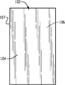
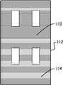
도 1은 백플레인에 포함되는 금속 박의 평면도이다.
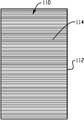
도 2는 절연체 및/또는 접착제가 제 1 표면 또는 전면, 가능하면 금속 박의 제 2 표면 또는 후면에 부착된 이후에 백플레인의 평면도이다.
도 3은 백플레인에 형성된 얇은 전도성 트레이스를 도시한다.
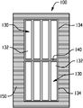
도 4는 백플레인의 제 1 표면 위에 개별 밀폐 엣지 실 없이 OLED 디바이스를 근접하게 위치시키는 것을 도시한다.
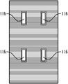
도 5는 백플레인의 금속 박에 형성되는 개구를 도시하는 평면도이다.
도 6은 도 5의 백플레인의 금속 박 부분의 전면 및 후면에 적용되는 절연체 및/또는 접착제의 평면도이다.
도 7은 금속 박을 통과하는 개구와 함께 실질적으로 정렬되는 절연체의 개구의 형성을 예시하는 평면도이다.
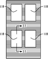
도 8은 절연체 및 금속 박 백플레인을 통과하여 형성되는 개구 위에 위치되는 금속 패치를 도시한다.
도 9는 백플레인 상에 OLED를 위치시키는 것을 도시한다.
도 10은 백플레인의 후면의 평면도이다.
도 11은 도 8의 라인 11-11을 따라 일반적으로 촬영되는 확대된 단면도이다.1 is a plan view of a metal foil included in a backplane.
FIG. 2 is a plan view of the backplane after the insulator and / or adhesive have been attached to the first surface or front side, possibly the second surface or back side of the metal foil.
3 shows a thin conductive trace formed on the backplane.
FIG. 4 shows the proximity of the OLED device without the individual hermetic edge seals on the first surface of the backplane.
5 is a plan view showing an opening formed in the metal foil of the backplane.
6 is a plan view of an insulator and / or adhesive applied to the front and back of the metal foil portion of the backplane of FIG.
7 is a plan view illustrating the formation of an opening in an insulator that is substantially aligned with the opening through the metal foil.
8 shows a metal patch located over an opening formed through an insulator and a metal foil backplane.
9 illustrates positioning the OLED on the backplane.
10 is a top view of the backside of the backplane.
FIG. 11 is an enlarged cross sectional view generally taken along line 11-11 of FIG. 8.
도 1 내지 도 4에 도시된 제 1 예시적인 실시예를 참조하면, 대면적 광원(100)은 설치의 상이한 단계에 대해 도시된다. 구체적으로, 금속 박(102)은 백플레인의 일부분을 형성한다. 금속 박(102)은 일반적으로 직사각형 형태를 갖는 것으로서 도시되지만, 다른 구성이 본 발명의 범위 및 의도로부터 벗어남이 없이 사용될 수 있다. 금속 박(102)은 얇아서, 예를 들어 약 25 마이크로미터 단위의 두께를 갖고, 다시 한번 이러한 두께는 오직 예시적인 것으로 간주되며, 금속 박은 전도성, 가요성 및 산소 및 습기에 대해 불투과성인 바람직한 품질을 제공한다. 바람직한 실시예에서, 금속 박은 실질적으로 전체 범위에 걸쳐 균일하며, 즉, 금속 박막은 제 1 표면 또는 전면(104), 제 2 표면 또는 후면(106)(도시되지 않음)에 걸쳐, 그리고 둘레(107)의 내부로부터 일반적으로 동일한 재료 특성 및 크기를 갖는다.With reference to the first exemplary embodiment shown in FIGS. 1-4, the large
도 2에서, 금속 박의 제 1 표면(104)은 이에 적용되는 절연체(110)와 함께 도시된다. 바람직하게, 절연체(110)는 금속 박의 엣지(107)를 커버하는 둘레 또는 엣지(112)를 포함하는 금속 박막의 전체 제 1 표면을 코팅하는 얇은 폴리머 또는 플라스틱 재료이다. 일부 경우에서 금속 박의 제 2 표면(106)(도시되지 않음)은 절연체와 함께 제공되지 않지만, 다른 용례에서 제 2 표면(106)에 절연체를 부착하고및/또는 제 1 및 제 2 표면 및 둘레를 포함한 금속 박을 완전하게 캡슐화하는 것이 바람직함이 이해될 것이다. 다시 한번, 예시의 방식으로만, 절연체는 약 25 마이크로미터 두께의 단위가 될 수 있고 금속 박의 전체 표면을 커버한다. 또한, 접착제는 종종 금속 박의 전면(104) 및/또는 후면(106)에 부착될 수 있다. 예시적인 실시예에서 접착제는 절연체에 사용된 재료와 동인한 재료이거나 에폭시 기반 접착제(epoxy based adhesive), 용융 열가소성 접착체(melt thermoplastic adhesive), 또는 압력 민감성 접착제(pressure sensitive adhesive)와 같은 별도 층이 될 수 있지만, 이하에서 설명된 목적에 적합한 임의의 재료가 사용될 수 있다. 접착제는 참조 번호 114로 나타내지만 절연체가 불투과성 금속 박을 커버하고 백플레인에 OLED를 접착하여 고정하는 것의 두 목적을 제공할 수 있기 때문에 도 2에서 분리 구조 층으로서 도시되지 않는다. 엣지 실을 통한 진입 및 OLED 디바이스 내에서의 후속 결함 형성을 방지하기 위해서, 절연체 재료는 산소 및 습기에 대해 저투과성을 갖는 것이 바람직하다. In FIG. 2, the
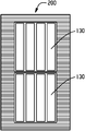
도 3은 백플레인, 특히 금속 박막의 제 1 표면(104)을 커버하는 절연체(110) 상에 형성되는 얇은 전도성 트레이스(120)의 일례를 도시한다. 트레이스(120)는 개수가 다양할 수 있지만, 백시트 상에 마운팅되는 각 OLED 디바이스에 대해 제 1 및 제 2 트레이스를 제공하는 것이 일반적이다. 전도성 트레이스(120)를 형성하는 임의의 편리한 방식은 예를 들어 스크린 프린팅, 증착 등이 사용될 수 있다. 트레이스(120)는 얇고 약 1 마이크론 두께이다. 도 3에서 바람직하게 예시된 바와 같이, 트레이스는 엣지 커넥터(도시되지 않음)와의 전기 접촉을 설정하기 위하여 절연체 또는 백플레인의 엣지(112)를 따라 형성된 제 1 말단(122)으로부터 내부로 연장되며, 도 4에서 도시된 바와 같이, 각 발광 디바이스, 또는 OLED(130)와 연관된 전극과의 접속을 위한 백플레인의 표면 상의 사전결정된 위치에 있는 제 2 말단(124)에서 끝난다. 예시적인 실시예에서, 각 OLED 디바이스(130)는 약 5cm2 내지 100cm2 크기의 범위이고, 바람직하게는 이의 엣지 또는 둘레를 따라 밀봉되지 않는다. 이 방식으로, 각 OLED 디바이스(130)의 실질적으로 모든 외부로 대면한 제 1 표면 또는 외부 표면(132)은 발광하는 것이다. 또한, 개별 OLED 디바이스의 각각에 대해 제공되는 밀폐 엣지 실이 없기 때문에, 각 OLED 디바이스의 둘레 엣지(134)는 더 근접한 관계가 될 수 있으며, 즉, 인접 OLED의 엣지에 대해 더 근접하게 이격될 수 있다. 인접한 OLED의 이 근접한 배치는 도 4에서 도시된 두 OLED 디바이스(130) 사이의 간격 또는 간극(140)을 이롭게 최소화한다. 이 간극(140)은 예를 들어 1mm 단위로, 가능한 작아질 수 있지만, 배치간격을 최소화하고 필 팩터를 증가시키는 것은 일반적인 목적이어서 실제 크기 값은 용례마다 다를 수 있다.3 shows an example of a thin
그 다음, 원하는 개수의 OLED 디바이스가 금속 박, 절연체, 접착제, 전도성 트레이스 등으로 구성된 백플레인 상에 마운팅되면, 둘레 또는 엣지 실(150)은 또한 백플레인 상에 설치되거나 마운팅된 OLED의 둘레에 대해 제공된다. 일부 경우에, 엣지 실은 외부 둘레 전체 및 백플레인의 제 2 표면 또는 후면 상에서 확장될 수 있다. 밀폐 엣지 실은 산소 및 습기로부터의 바람직한 보호를 제공하고, 약 10mm 단위의 상대적인 공칭 두께 또는 폭을 갖는다. 이 상대적으로 넓은 폭은 가요성 OLED를 캡슐화하기 위해 사용되는 폴리머 접작체가 본질적으로 다공성(porous)이어서 산소 및 수증기가 대량의 재료를 통과하여 서서히 확산하게 한다는 사실에 기인한다. 10mm와 같은, 긴 투과 경로 길이를 가짐으로써, 수분과 산소가 재료를 통과하여 확산하고 OLED 디바이스에 반응하게 하는 시간을 상당히 연장시키는 것이 가능하여, 밀폐 실을 제공하고 제품에 허용가능한 보관 수명(shelf life)을 제공한다. 이 방식으로, 밀폐 실이 어셈블리 위에 적용되기 이전에, 개별 비캡슐화된 OLED(130)는 함께 타일링, 즉, 백플레인에 접착되어 고정된다. 따라서 발광 패널(100)의 필링 팩터는 상당히 개선된다. 즉, 각 개별 OLED는 캡슐화된 엣지 실을 포함하지 않기 때문에, 엣지 실의 폭은 각 OLED 디바이스로부터 제거되고 인접 OLED 디바이스가 함께 더 근접하게 위치되는 것을 허용하여서 간극(140)의 크기를 최소화한다. 다시 한번, 필링 팩터, 즉, 패널의 총 표면적에 대한 조명 면적의 비율이 최대화된다. 광을 방출하는 OLED 패널의 총 표면적의 양을 증가시키는 것은 패널으로부터의 전체 광 또는 루멘(lumen)에서의 상당한 개선을 의미한다. 필 팩터에서의 개선은 개별 OLED 디바이스의 크기, 패널에서 타일링된 디바이스의 개수, 및 밀폐 엣지 실의 원하는 폭에 따라 급격히 다를 수 있다. 예시로서, 아홉 개의 5cm x 5cm 디바이스가 큰 정사각 패널로 타일링되면, 비캡슐화된 OLED에 대해 1cm 밀폐 엣지 실 및 1mm의 간극을 가정하여, 캡슐화 이전에 비캡슐화된 OLED를 타일링함으로써 필 팩터가 50%에서 70%로 개선될 수 있다.Then, if the desired number of OLED devices are mounted on a backplane composed of metal foil, insulators, adhesives, conductive traces, etc., a circumferential or
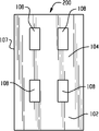
제 2 실시예가 도 5 내지 도 11에 도시된다. 많은 특징이 유사하기 때문에, 유사한 참조 번호는 유사한 요소를 지칭할 것이고 새로운 컴포넌트는 새로운 참조 번호로 식별된다. 예를 들어, 대면적 광 어셈블리는 200으로서 참조된다. 다시 한번 백플레인은 제 1 표면 또는 상위 표면(104) 및 제 2 표면 또는 하위 표면(106)(도시되지 않음) 및 둘레 또는 엣지(107)를 갖는 금속 박막(102)을 포함하고, 따라서 금속 박이 실질적으로 변경되지 않기 때문에 도 1에 대한 참조가 이루어진다. 선택된 내부 영역에서 금속 박을 관통하여 컷팅되거나 펀칭되는 것 등에 의해 개구 또는 구멍(108)이 금속 박(도 5)에서 형성된다. 이하에서 더 명확해지는 바와 같이 이 개구(108)는 금속 박(102)의 전체 두께를 관통하기 위한 것이고 백플레인 상에서 타일링되는 OLED와의 전기 접속을 위한 사전선택된 위치에 위치된다. 예시의 목적을 위해, 네 개의 이러한 개구(108)가 개구가 아니었더라면 불투과성인 금속 박에 형성되고 각 개구는 실질적으로 동일한 크기를 갖지만, 본 발명은 개구가 모두 동일한 구성에 제한되지 않는다.A second embodiment is shown in Figures 5-11. Because many features are similar, like reference numerals will refer to like elements and new components are identified with new reference numbers. For example, the large area light assembly is referred to as 200. Once again the backplane comprises a
도 2에 대해 도시되고 설명된 바와 같은 대체로 동일한 방식으로 다시 한번, 절연체(110)가 금속 박(102)의 전면(104) 및 후면(106)에 적용된다. 또한, 절연체(110)가 금속 박에 이전에 형성된 개구(108)를 커버할 것임이 의도된다. 바람직하게는, 접착제(114)는 또한 OLED 디바이스를 후속하여 고정시키기 위해 적어도 제 1 표면에 적용된다. Once again in an almost identical manner as shown and described with respect to FIG. 2, an
도 7에서 도시된 바와 같이, 더 작은 개구 또는 구멍(116)이 절연체(110)를 관통하여 컷팅되고 금속 박을 통과하는 개구(108)에 대해 중심에 존재하며, 바람직하게는 금속 박을 통과하여 형성되는 개구(108)보다 약간 더 작다. 이 방식으로, 절연체가 개구(108)의 전체 내부 둘레 엣지를 커버하기 때문에 금속 박과 의도하지 않은 접촉이 발생할 가능성이 적다. 비록 도 7의 개구의 각각은 동일한 크기가 되도록 도시되었지만, 절연체를 통과하는 이 개구(116)는 크기가 다를 수 있고, 중요하게는 백플레인의 제 1 표면 또는 전면(104)에서부터 제 2 표면 또는 후면(106)까지의 전기 접촉을 가능하게 한다는 것이다.As shown in FIG. 7, a smaller opening or
도 8에서, 개별 금속 패치(118)는 백플레인에서 개구(108, 116)를 가로놓도록 크기조정되고 라미네이트 프로세스(a lamination process)를 통해 전면(104)에 고정된다. 밀폐 엣지 실이 없는 개별 OLED 디바이스가 백플레인의 전면(104) 상의 절연체(110) 상에 배치된 접착제(114)를 통해 패널에 고정될 때, OLED 디바이스(130)의 전극(도시되지 않음)은 각각의 전기 패치(118) 중 하나에 전기적으로 접속될 수 있고, 연관된 전자 드라이버(도시되지 않음)와 패치의 전기 접속이 완성된다. 도 10에서 또한 도시된 바와 같이, 패치(118)의 전면은 절연체의 개구(116)를 통과하여 액세스가능하고 개구가 아니라면 불투과성인 금속 박을 통과하는 개구(108) 내에서 유사하게 형성된다. 이 방식으로, 전기 접속은 백플레인의 후면 상에서 완성될 수 있고 이러한 접속은 OLED의 발광 표면(132)과 간섭하지 않는다. 도 11에서 더 도시된 것처럼, 불투과성 금속 박(102)의 전면과 후면 상에 제공되는 접착제/절연체(110)를 관통하는 개구(116)가 패치(118)로의 접속을 허용한다.In FIG. 8,
도 1 내지 도 4와 함께 실시예로 언급된 바와 같이, 도 5 내지 도 11의 실시예 또한 밀폐 엣지 실을 갖지 않는 개별 OLED 디바이스를 사용한다. 그 결과로서, 각 OLED는 다음 인접 OLED와 더 근접하게 이동될 수 있고 따라서 간극(140)의 크기는 인접한, 타일링된 OLED 사이에서 최소화된다. 다시 한번, 이 구성은 패널의 필 팩터를 최대화하여서 백플레인의 전체 표면 중 더 큰 비율이 이에 고정된 개별 OLED 디바이스에 의해 제공되는 발광 표면적으로 커버된다. 그 결과로서, 광 출력은 최대화된다. 밀폐 엣지 실(150)은 대면적 광 어셈블리(200)의 전체 둘레 영역 을 둘러싸면서 제공되고, 산소 또는 습기의 해로운 영향으로부터 어셈블리를 보호하는 바람직한 캡슐화를 제공한다.As mentioned in the examples in conjunction with FIGS. 1-4, the embodiments of FIGS. 5-11 also use individual OLED devices that do not have a closed edge seal. As a result, each OLED can be moved closer to the next adjacent OLED so that the size of the
이 실시예의 각각은 또한 투명하고 OLED 디바이스의 상부에 라미네이트되는 초고차단성 필름을 사용한다. 이 차단성 필름은 패키지의 엣지로 연장하는 전기 리드(lead)를 갖는 밀폐 패키지를 생성하거나(도 1 내지 도 4의 실시예와 같이) 또는 엣지 커넥터 없이 밀폐 패키지를 생성한다(도 5 내지 도 11의 실시예에서 도시됨).Each of these examples also uses a super high barrier film that is transparent and laminates on top of the OLED device. This barrier film creates a sealed package with electrical leads extending to the edge of the package (as in the embodiment of FIGS. 1-4) or creates a sealed package without an edge connector (FIGS. 5-11). Shown in the examples of).
OLED 디바이스를 백플레인 및 UHB 필름의 전면에 접착하여 본딩하는 것은 이전 구성을 뛰어넘는 장점을 제공한다. 예를 들어, OLED 디바이스를 초고차단성 필름에 부착하는 것은 재료를 광학적으로 연결하고, 더 많은 광이 빠져나가도록 한다. 아마 더 중요한 것은, UHB 필름 및 백플레인에 OLED를 접착하여 고정하는 것이 라미네이트 프로세스 동안 기체의 트래핑(trapping)을 방지한다는 것이다. 접착제 없이, 기체의 포켓(pocket)은 라미네이트 프로세서 동안 트래핑될 수 있고, 유연한 용례에서 원치않는 응력 및 잠재적인 박리 결함(potential delamination defects)을 야기하는, 이 기체 포켓은 밀폐 패널 내에서 이동할 수 있다. 패널에서 트래핑된 기체 거품을 갖는 것은 또한 미적으로 좋지 않다. 전체 UHB 필름(패키지의 내부) 위에 배치되는 접착제를 갖는 것과 전체 백시트 위에 접착제를 갖는 것(전기 접촉이 OLED와 함께 이루어지는 곳은 제외)은 바람직한 실시예이다. 접착제는 열가소성, 열경화성(thermosetting), PSA, 또는 조합이 될 수 있다.Bonding and bonding OLED devices to the front of the backplane and UHB film offers advantages over previous configurations. For example, attaching an OLED device to an ultra high barrier film optically connects the material and allows more light to escape. Perhaps more importantly, bonding and fixing the OLED to the UHB film and backplane prevents trapping of gases during the laminate process. Without adhesive, a pocket of gas can be trapped during the laminate processor, and this gas pocket can move within the closure panel, causing unwanted stresses and potential delamination defects in flexible applications. Having gas bubbles trapped in the panel is also not aesthetically good. Having an adhesive disposed over the entire UHB film (inside the package) and having the adhesive over the entire backsheet (except where electrical contact is made with the OLED) is a preferred embodiment. The adhesive can be thermoplastic, thermosetting, PSA, or a combination.
대면적 가요성 OLED 광원의 방법 및 디자인이 제공된다. 밀폐 엣지 실이 없는 개별 소면적 가용성 OLED가 제조되고 OLED를 전기적으로 접속시키는 수단을 제공하는 더 큰 패널로 집적되며, 전체 시스템의 유연성을 유지하면서 OLED를 밀폐하여 캡슐화한다. 다른 실시예에서, 필링 팩터를 최대화하는 특성은 원하지만 유연성은 중요하지 않은 경우 비가요성 버전이 또한 사용가능하다. 제조 성능 및 물성 제한에 기인하여, 개별 OLED 디바이스의 크기는 통상적으로 상대적으로 작은 크기에 제약된다. 따라서, 위에서 설명된 바와 같은 대면적 광 패널을 획득하기 위해, 개별 OLED는 각각 밀폐 엣지 실을 갖지 않으면서 더 큰 패널을 형성하기 위해 함께 타일링된다. 각각의 개별 OLED 상에서 엣지 실링을 제거함으로써, 이 디바이스가 더 큰 패널로 조립될 때, 전체 패널의 필 팩터, 즉, 패널 내에서 조명 면적의 비율이 증가된다. 개별 OLED는 비캡슐화된 형태로 함께 타일링되고 그 다음 모든 개별 OLED가 표면에 고정되면 밀폐 실이 전체 어셈블리에 적용된다. 백플레인, OLED 및 투명 캡슐화 층은 대면적 패널을 위해 제공된다. 백플레인은 불투과성이고, 이 구성에서 대면적 패널의 하나 이상의 OLED 디바이스를 전기적으로 접속시키기 위한 전도성 네트워크를 제공한다. 이 구성은 또한 유연성을 유지할 수 있다. 백플레인은 또한 관련 전기 드라이버로의 외부 접속을 위한 수단을 포함한다. 밀폐 실이 여전히 만들어져야하기 때문에, 전도성 트레이스를 최적화하는 것이 중요하다. 얇고 좁은 트레이스의 사용은 장거리에 걸쳐 상당한 전력 손실을 가질 수 있다. 따라서, 가변 트레이스 두께의 디자인 또는 재료 선택조차도 이 이슈의 일부를 해결할 수 있다. 초기에 비캡슐화된 OLED를 사용함으로써 밀폐 엣지 실이 존재하지 않으면, OLED가 최소 간격으로 배치될 수 있게 하여 방출 면적의 필링 팩터의 대응하는 증가를 가능하게 한다. 최종적으로, 캡슐화층이 전체 패널에 적용되고, 산소 및 습기로부터 패널을 보호한다.A method and design of a large area flexible OLED light source is provided. Individual small area soluble OLEDs without sealed edge seals are fabricated and integrated into larger panels that provide a means to electrically connect the OLEDs, encapsulating and encapsulating the OLEDs while maintaining the flexibility of the entire system. In another embodiment, a non-flexible version is also available if a feature that maximizes the filling factor is desired but flexibility is not important. Due to manufacturing performance and property limitations, the size of individual OLED devices is typically limited to relatively small sizes. Thus, to obtain a large area light panel as described above, the individual OLEDs are tiled together to form larger panels without each having a sealed edge seal. By eliminating edge sealing on each individual OLED, when the device is assembled into larger panels, the fill factor of the entire panel, i.e., the proportion of illumination area within the panel, is increased. The individual OLEDs are tiled together in an unencapsulated form, and then all the individual OLEDs are fixed to the surface and the seal is applied to the entire assembly. Backplanes, OLEDs and transparent encapsulation layers are provided for large area panels. The backplane is impermeable and in this configuration provides a conductive network for electrically connecting one or more OLED devices of the large area panel. This configuration can also maintain flexibility. The backplane also includes means for external connection to the associated electric driver. Since sealed seals still have to be made, it is important to optimize the conductive traces. The use of thin and narrow traces can have significant power loss over long distances. Thus, even the design or material selection of variable trace thickness can solve some of this issue. The use of initially unencapsulated OLEDs allows the OLEDs to be placed at minimal intervals in the absence of a sealed edge seal, thereby enabling a corresponding increase in the filling factor of the emission area. Finally, an encapsulation layer is applied to the entire panel and protects the panel from oxygen and moisture.
본 실시예는 바람직한 실시예를 참조하여 설명되었다. 명백하게, 다른 사람들이 전술된 상세한 설명을 판독하고 이해할 시에 수정 및 변경이 발생할 것이다. 본 실시예는 모든 이러한 수정 및 변경을 포함하는 것으로서 이해되도록 의도된다.This embodiment has been described with reference to the preferred embodiment. Obviously, modifications and changes will occur when others read and understand the foregoing detailed description. This embodiment is intended to be understood as including all such modifications and variations.
Claims (23)
기판의 상기 제 1 표면 상에 수용되는 적어도 제 1 발광 디바이스 및 제 2 발광 디바이스―상기 제 1 발광 디바이스 및 상기 제 2 발광 디바이스 각각은 상기 제 1 표면적보다 작은 표면적을 갖고 상기 백플레인의 전기적으로 전도성인 부분에 전기적으로 접속됨―와,
적어도 상기 제 1 발광 디바이스 및 상기 제 2 발광 디바이스 위에 연장되어 적어도 상기 제 1 발광 디바이스 및 상기 제 2 발광 디바이스를 밀봉하는(hermetically sealing) 캡슐화 재료(an encapsulation material)와,
연관된 전기 드라이버에 접속하기 위한 전기 경로(an electrical path)를 포함하는
발광 어셈블리.
A backplane having a first surface area and comprising an electrically conductive portion on at least a first surface of the first surface area,
At least a first light emitting device and a second light emitting device received on the first surface of the substrate, each of the first light emitting device and the second light emitting device having a surface area less than the first surface area and being electrically conductive of the backplane. Electrically connected to the portion—,
An encapsulation material extending over at least the first light emitting device and the second light emitting device and sealing at least the first light emitting device and the second light emitting device;
An electrical path for connecting to an associated electrical screwdriver
Luminous assembly.
캡슐화는 상기 제 1 발광 디바이스 및 상기 제 2 발광 디바이스를 밀봉하는 것인
발광 어셈블리.
The method of claim 1,
Encapsulation seals the first light emitting device and the second light emitting device
Luminous assembly.
상기 제 1 발광 디바이스 및 상기 제 2 발광 디바이스는 OLED인
발광 어셈블리.
The method of claim 1,
The first light emitting device and the second light emitting device are OLED
Luminous assembly.
상기 백플레인은 가요성(flexible)인
발광 어셈블리.
The method of claim 1,
The backplane is flexible
Luminous assembly.
상기 백플레인은 비가요성(non-flexible)인
발광 어셈블리.
The method of claim 1,
The backplane is non-flexible
Luminous assembly.
개별적인 상기 적어도 제 1 발광 디바이스 및 상기 제 2 발광 디바이스의 각각은 필링 팩터(filling factor)를 최대화하기 위해 상기 백플레인 상으로 수용되기 이전에 개별 밀폐 엣지 실(hermetic edge seal)을 갖지 않는
발광 어셈블리.
The method of claim 1,
Each of the individual at least first and second light emitting devices does not have a separate hermetic edge seal prior to being received onto the backplane to maximize the filling factor.
Luminous assembly.
상기 전기 경로는 상기 백플레인의 표면을 따라 형성되는 전도성 트레이스(conductive trace)를 포함하는
발광 어셈블리.
The method of claim 1,
The electrical path includes a conductive trace formed along the surface of the backplane.
Luminous assembly.
상기 캡슐화 재료는 광 투과성(light transmissive)인
발광 어셈블리.
The method of claim 1,
The encapsulation material is light transmissive
Luminous assembly.
상기 백플레인은 산소 및 수증기에 대해 불투과성(impermeable)인
발광 어셈블리.
The method of claim 1,
The backplane is impermeable to oxygen and water vapor
Luminous assembly.
상기 발광 디바이스는 직렬, 병렬, 독립적, 또는 단일 공통 버스 중 하나로 접속되는
발광 어셈블리.
The method of claim 1,
The light emitting device is connected to one of the serial, parallel, independent, or single common bus
Luminous assembly.
상기 백플레인은 절연체로 커버되는 제 1 표면을 갖는 불투과성 금속 박(impermeable metal foil)을 포함하는
발광 어셈블리.
The method of claim 1,
The backplane includes an impermeable metal foil having a first surface covered with an insulator.
Luminous assembly.
상기 백플레인은 상기 금속 박의 절연체에 정렬된 개구 및 상기 개구 위에 수용된 전기적으로 전도성인 패치를 포함하고, 적어도 상기 제 1 발광 디바이스 및 상기 제 2 발광 디바이스는 상기 패치에 전기적으로 접속되는
발광 어셈블리.
The method of claim 11,
The backplane includes an opening aligned with the insulator of the metal foil and an electrically conductive patch received over the opening, wherein at least the first light emitting device and the second light emitting device are electrically connected to the patch.
Luminous assembly.
상기 절연체는 불투과성 층을 캡슐화하는
발광 어셈블리.
The method of claim 11,
The insulator encapsulates the impermeable layer
Luminous assembly.
절연 층은 전도성 층과 상기 전기적으로 전도성인 부분 사이에 삽입(interposed)되는
발광 어셈블리.
The method of claim 11,
An insulating layer is interposed between the conductive layer and the electrically conductive portion.
Luminous assembly.
상기 전기적으로 전도성인 부분은 절연 층 상의 트레이스인
발광 어셈블리.
The method of claim 11,
The electrically conductive portion is a trace on the insulating layer
Luminous assembly.
필링 팩터를 최대화하고 인접 OLED 사이의 갭을 최소화하기 위해 OLED들 사이에 밀폐 엣지 실 없이 상기 백플레인 상에 근접하게 위치되는 제 1 OLED 및 제 2 OLED와,
상기 제 1 OLED, 상기 제 2 OLED 및 기판의 제 1 표면 위의 캡슐화 재료를 포함하는
광 어셈블리.
A backplane having a first surface thereon including a conductive portion thereon;
First and second OLEDs located in close proximity to the backplane without sealing edge seals between the OLEDs to maximize the fill factor and minimize gaps between adjacent OLEDs;
An encapsulation material on the first OLED, the second OLED, and the first surface of the substrate.
Optical assembly.
상기 백플레인은 가요성인
광 어셈블리.
17. The method of claim 16,
The backplane is flexible
Optical assembly.
상기 백플레인은 비가요성인
광 어셈블리.
17. The method of claim 16,
The backplane is inflexible
Optical assembly.
백플레인을 제공하는 단계와,
상기 백플레인 상에 엣지 실(edge seals)을 갖는 개별 OLED를 근접하게 설치하는 단계와,
상기 백플레인 상의 상기 OLED를 밀봉하는 단계를 포함하는
OLED 광원 형성 방법.
In the method of forming an OLED light source,
Providing a backplane,
Close installation of individual OLEDs with edge seals on the backplane;
Sealing the OLED on the backplane
OLED light source formation method.
상기 밀봉하는 단계 이전에 상기 백플레인 상의 전도성 부분에 상기 OLED를 전기적으로 접속시키는 단계를 더 포함하는
OLED 광원 형성 방법.
The method of claim 19,
Electrically connecting the OLED to a conductive portion on the backplane prior to the sealing step
OLED light source formation method.
상기 실링하는 단계는 상기 백플레인에 상기 OLED를 접착하여 실링하는(adhesively sealing) 단계를 더 포함하는
OLED 광원 형성 방법.
The method of claim 19,
The sealing step further includes the step of adheringly sealing the OLED to the backplane.
OLED light source formation method.
상기 OLED를 상기 OLED 위에 수용된 초고차단성 필름(an ultrahigh barrier film)에 접착하여 실링하는 단계를 더 포함하는
OLED 광원 형성 방법.
22. The method of claim 21,
Bonding the OLED to an ultrahigh barrier film housed on the OLED to seal the OLED;
OLED light source formation method.
상기 OLED를 상기 OLED 위에 수용된 초고차단성 필름에 접착하여 실링하는 단계를 더 포함하는
OLED 광원 형성 방법.The method of claim 19,
Bonding the OLED to an ultra-high barrier film accommodated on the OLED to seal
OLED light source formation method.
Applications Claiming Priority (3)
| Application Number | Priority Date | Filing Date | Title |
|---|---|---|---|
| US12/782,228 | 2010-05-18 | ||
| US12/782,228 US8618731B2 (en) | 2010-05-18 | 2010-05-18 | Large-area flexible OLED light source |
| PCT/US2011/036570 WO2011146350A1 (en) | 2010-05-18 | 2011-05-16 | Large-area flexible oled light source |
Publications (1)
| Publication Number | Publication Date |
|---|---|
| KR20130097075A true KR20130097075A (en) | 2013-09-02 |
Family
ID=44343070
Family Applications (1)
| Application Number | Title | Priority Date | Filing Date |
|---|---|---|---|
| KR1020127030170A KR20130097075A (en) | 2010-05-18 | 2011-05-16 | Large-area flexible oled light source |
Country Status (7)
| Country | Link |
|---|---|
| US (1) | US8618731B2 (en) |
| EP (1) | EP2572379A1 (en) |
| JP (1) | JP5849091B2 (en) |
| KR (1) | KR20130097075A (en) |
| CN (1) | CN102893395B (en) |
| TW (1) | TW201212325A (en) |
| WO (1) | WO2011146350A1 (en) |
Families Citing this family (10)
| Publication number | Priority date | Publication date | Assignee | Title |
|---|---|---|---|---|
| US10061356B2 (en) | 2011-06-30 | 2018-08-28 | Samsung Display Co., Ltd. | Flexible display panel and display apparatus including the flexible display panel |
| WO2013114295A1 (en) | 2012-02-03 | 2013-08-08 | Koninklijke Philips N.V. | Oled device and manufacture thereof |
| WO2014059601A1 (en) * | 2012-10-16 | 2014-04-24 | 深圳市柔宇科技有限公司 | Oled mosaic display screen and manufacturing method thereof |
| DE102012223162B4 (en) | 2012-12-14 | 2022-08-25 | Pictiva Displays International Limited | AREA LIGHT SYSTEM |
| CN104080219A (en) * | 2013-03-29 | 2014-10-01 | 海洋王照明科技股份有限公司 | Oled lamp |
| JP6131719B2 (en) * | 2013-05-28 | 2017-05-24 | コニカミノルタ株式会社 | Reflecting member, manufacturing method thereof, and surface emitting unit |
| JP2014232156A (en) * | 2013-05-28 | 2014-12-11 | コニカミノルタ株式会社 | Reflection member and surface light emission unit |
| JPWO2015118932A1 (en) * | 2014-02-10 | 2017-03-23 | コニカミノルタ株式会社 | Organic electroluminescence lighting device and lighting method |
| JP6907032B2 (en) | 2017-06-06 | 2021-07-21 | 株式会社ジャパンディスプレイ | Display device and its manufacturing method |
| WO2019230617A1 (en) * | 2018-05-31 | 2019-12-05 | コニカミノルタ株式会社 | Surface light emission panel and method for manufacturing surface light emission panel |
Family Cites Families (32)
| Publication number | Priority date | Publication date | Assignee | Title |
|---|---|---|---|---|
| US6204453B1 (en) * | 1998-12-02 | 2001-03-20 | International Business Machines Corporation | Two signal one power plane circuit board |
| US6370019B1 (en) * | 1998-02-17 | 2002-04-09 | Sarnoff Corporation | Sealing of large area display structures |
| US6897855B1 (en) * | 1998-02-17 | 2005-05-24 | Sarnoff Corporation | Tiled electronic display structure |
| US6175087B1 (en) * | 1998-12-02 | 2001-01-16 | International Business Machines Corporation | Composite laminate circuit structure and method of forming the same |
| JP2001100668A (en) * | 1999-09-29 | 2001-04-13 | Sanyo Electric Co Ltd | Electroluminescence display device |
| TWI273722B (en) | 2000-01-27 | 2007-02-11 | Gen Electric | Organic light emitting device and method for mounting |
| US6515417B1 (en) * | 2000-01-27 | 2003-02-04 | General Electric Company | Organic light emitting device and method for mounting |
| US6930256B1 (en) * | 2002-05-01 | 2005-08-16 | Amkor Technology, Inc. | Integrated circuit substrate having laser-embedded conductive patterns and method therefor |
| US7005799B2 (en) * | 2001-07-30 | 2006-02-28 | Intel Corporation | Sealing organic light emitting device displays |
| US6888307B2 (en) * | 2001-08-21 | 2005-05-03 | Universal Display Corporation | Patterned oxygen and moisture absorber for organic optoelectronic device structures |
| AU2002351047A1 (en) | 2001-12-17 | 2003-06-30 | Koninklijke Philips Electronics N.V. | Tiled flat panel display, method of manufacturing the same, and sub-display for use in such a display, and method of driving such a display |
| JP3942017B2 (en) | 2002-03-25 | 2007-07-11 | 富士フイルム株式会社 | Light emitting element |
| JP2003297561A (en) * | 2002-03-29 | 2003-10-17 | Fuji Photo Film Co Ltd | Manufacturing method of organic film element and organic film element |
| US6642092B1 (en) * | 2002-07-11 | 2003-11-04 | Sharp Laboratories Of America, Inc. | Thin-film transistors formed on a metal foil substrate |
| US7049757B2 (en) * | 2002-08-05 | 2006-05-23 | General Electric Company | Series connected OLED structure and fabrication method |
| US20060208634A1 (en) * | 2002-09-11 | 2006-09-21 | General Electric Company | Diffusion barrier coatings having graded compositions and devices incorporating the same |
| US7015640B2 (en) * | 2002-09-11 | 2006-03-21 | General Electric Company | Diffusion barrier coatings having graded compositions and devices incorporating the same |
| US7018713B2 (en) * | 2003-04-02 | 2006-03-28 | 3M Innovative Properties Company | Flexible high-temperature ultrabarrier |
| US7052355B2 (en) * | 2003-10-30 | 2006-05-30 | General Electric Company | Organic electro-optic device and method for making the same |
| EP1712109A4 (en) * | 2003-12-30 | 2008-03-19 | Agency Science Tech & Res | Flexible electroluminescent devices |
| US8405193B2 (en) * | 2004-04-02 | 2013-03-26 | General Electric Company | Organic electronic packages having hermetically sealed edges and methods of manufacturing such packages |
| US7108392B2 (en) * | 2004-05-04 | 2006-09-19 | Eastman Kodak Company | Tiled flat panel lighting system |
| JP4289332B2 (en) * | 2004-09-30 | 2009-07-01 | セイコーエプソン株式会社 | EL display device, method for manufacturing EL display device, and electronic apparatus |
| JP2006163325A (en) * | 2004-11-11 | 2006-06-22 | Fuji Electric Holdings Co Ltd | Organic el display |
| KR100696479B1 (en) * | 2004-11-18 | 2007-03-19 | 삼성에스디아이 주식회사 | Organic light emitting device and method for fabricating the same |
| US20070200489A1 (en) * | 2006-02-01 | 2007-08-30 | Poon Hak F | Large area organic electronic devices and methods of fabricating the same |
| KR100748309B1 (en) * | 2006-02-10 | 2007-08-09 | 삼성에스디아이 주식회사 | Organic light-emitting display device and method for fabricating the same |
| US7973473B2 (en) * | 2007-03-02 | 2011-07-05 | Global Oled Technology Llc | Flat panel OLED device having deformable substrate |
| JP5208591B2 (en) * | 2007-06-28 | 2013-06-12 | 株式会社半導体エネルギー研究所 | Light emitting device and lighting device |
| US20090284158A1 (en) * | 2008-05-16 | 2009-11-19 | General Electric Company | Organic light emitting device based lighting for low cost, flexible large area signage |
| CN201354982Y (en) * | 2008-12-22 | 2009-12-02 | 北京巨数数字技术开发有限公司 | Backlight and LCD display employing same |
| KR101436994B1 (en) * | 2009-01-23 | 2014-09-11 | 삼성전자주식회사 | Foldable display apparatus |
-
2010
- 2010-05-18 US US12/782,228 patent/US8618731B2/en not_active Expired - Fee Related
-
2011
- 2011-05-16 JP JP2013511246A patent/JP5849091B2/en not_active Expired - Fee Related
- 2011-05-16 KR KR1020127030170A patent/KR20130097075A/en not_active Application Discontinuation
- 2011-05-16 EP EP11721677A patent/EP2572379A1/en not_active Withdrawn
- 2011-05-16 WO PCT/US2011/036570 patent/WO2011146350A1/en active Application Filing
- 2011-05-16 CN CN201180024477.8A patent/CN102893395B/en not_active Expired - Fee Related
- 2011-05-18 TW TW100117471A patent/TW201212325A/en unknown
Also Published As
| Publication number | Publication date |
|---|---|
| JP5849091B2 (en) | 2016-01-27 |
| US8618731B2 (en) | 2013-12-31 |
| JP2013531337A (en) | 2013-08-01 |
| CN102893395A (en) | 2013-01-23 |
| WO2011146350A1 (en) | 2011-11-24 |
| CN102893395B (en) | 2015-08-19 |
| TW201212325A (en) | 2012-03-16 |
| EP2572379A1 (en) | 2013-03-27 |
| US20110285273A1 (en) | 2011-11-24 |
Similar Documents
| Publication | Publication Date | Title |
|---|---|---|
| US8618731B2 (en) | Large-area flexible OLED light source | |
| TWI527281B (en) | Hermetic electrical package | |
| TW200507032A (en) | Display device and method of manufacturing thereof | |
| KR101983740B1 (en) | Thermal management in large area flexible oled assembly | |
| US8692457B2 (en) | Large area light emitting electrical package with current spreading bus | |
| TWI552329B (en) | Organic light emitting device connection methods | |
| JP2013531337A5 (en) | ||
| KR101805967B1 (en) | Low temperature contact structure for flexible solid state device | |
| US8427845B2 (en) | Electrical connectors for optoelectronic device packaging | |
| US10629844B2 (en) | Organic optoelectronic component and method for producing an organic optoelectronic component | |
| KR20170063593A (en) | Organic el panel and method for producing same | |
| CN102812575B (en) | Alleviate the short-circuit risks in packaged type organic light emitting apparatus (OLED) | |
| KR20140048208A (en) | Oled encapsulated in a full-wafer adhesive having a perforated cover | |
| US20160181326A1 (en) | Radiation-Emitting Apparatus and Method for Producing Same | |
| JPWO2019065430A1 (en) | Solar cell module and manufacturing method of solar cell module | |
| KR101997687B1 (en) | Method for manufacturing encapsulated electronic device | |
| JP2020181755A (en) | Manufacturing method of light-emitting device and light-emitting device | |
| KR20050014410A (en) | Organic electroluminescent device comprising the substrate with dummy pattern | |
| JP2016091713A (en) | Surface light-emitting module |
Legal Events
| Date | Code | Title | Description |
|---|---|---|---|
| A201 | Request for examination | ||
| E902 | Notification of reason for refusal | ||
| E601 | Decision to refuse application |