EP3264462A1 - Led module - Google Patents
Led module Download PDFInfo
- Publication number
- EP3264462A1 EP3264462A1 EP17179028.0A EP17179028A EP3264462A1 EP 3264462 A1 EP3264462 A1 EP 3264462A1 EP 17179028 A EP17179028 A EP 17179028A EP 3264462 A1 EP3264462 A1 EP 3264462A1
- Authority
- EP
- European Patent Office
- Prior art keywords
- led
- light
- emitting diode
- led devices
- light emitting
- Prior art date
- Legal status (The legal status is an assumption and is not a legal conclusion. Google has not performed a legal analysis and makes no representation as to the accuracy of the status listed.)
- Granted
Links
Images




Classifications
-
- F—MECHANICAL ENGINEERING; LIGHTING; HEATING; WEAPONS; BLASTING
- F21—LIGHTING
- F21K—NON-ELECTRIC LIGHT SOURCES USING LUMINESCENCE; LIGHT SOURCES USING ELECTROCHEMILUMINESCENCE; LIGHT SOURCES USING CHARGES OF COMBUSTIBLE MATERIAL; LIGHT SOURCES USING SEMICONDUCTOR DEVICES AS LIGHT-GENERATING ELEMENTS; LIGHT SOURCES NOT OTHERWISE PROVIDED FOR
- F21K9/00—Light sources using semiconductor devices as light-generating elements, e.g. using light-emitting diodes [LED] or lasers
- F21K9/60—Optical arrangements integrated in the light source, e.g. for improving the colour rendering index or the light extraction
- F21K9/62—Optical arrangements integrated in the light source, e.g. for improving the colour rendering index or the light extraction using mixing chambers, e.g. housings with reflective walls
-
- H—ELECTRICITY
- H10—SEMICONDUCTOR DEVICES; ELECTRIC SOLID-STATE DEVICES NOT OTHERWISE PROVIDED FOR
- H10W—GENERIC PACKAGES, INTERCONNECTIONS, CONNECTORS OR OTHER CONSTRUCTIONAL DETAILS OF DEVICES COVERED BY CLASS H10
- H10W90/00—Package configurations
-
- F—MECHANICAL ENGINEERING; LIGHTING; HEATING; WEAPONS; BLASTING
- F21—LIGHTING
- F21Y—INDEXING SCHEME ASSOCIATED WITH SUBCLASSES F21K, F21L, F21S and F21V, RELATING TO THE FORM OR THE KIND OF THE LIGHT SOURCES OR OF THE COLOUR OF THE LIGHT EMITTED
- F21Y2115/00—Light-generating elements of semiconductor light sources
- F21Y2115/10—Light-emitting diodes [LED]
-
- H—ELECTRICITY
- H10—SEMICONDUCTOR DEVICES; ELECTRIC SOLID-STATE DEVICES NOT OTHERWISE PROVIDED FOR
- H10H—INORGANIC LIGHT-EMITTING SEMICONDUCTOR DEVICES HAVING POTENTIAL BARRIERS
- H10H20/00—Individual inorganic light-emitting semiconductor devices having potential barriers, e.g. light-emitting diodes [LED]
- H10H20/80—Constructional details
- H10H20/85—Packages
- H10H20/855—Optical field-shaping means, e.g. lenses
- H10H20/856—Reflecting means
Definitions
- the present disclosure relates to an LED module.
- LED module in which a plurality of light emitting diode (LED) devices are arranged on a mounting board, see for example Japanese Patent Publication No. 2014-143246 .
- the lateral faces of the LED devices are each constructed with a phosphor member or a reflective member, and the plurality of LED devices are arranged so that the phosphor members of certain LED devices face the reflective members of certain LED Devices.
- the LED module disclosed in the above patent publication if the LED devices are arranged so that the reflective members are positioned along the outermost perimeter of the LED module, the light from the LED devices is reflected by the reflective member positioned along the outermost perimeter of the LED module to thereby reduce the light distribution of the LED module. In other words, it is difficult for the light from the LED devices to spread out from the outermost perimeter of the LED module, resulting in a narrow light distribution. Such an LED module is not suited for indoor lighting or the like, which requires a wide light distribution.
- the lateral faces constructed with a phosphor member in certain LED devices face the lateral faces constructed with a reflective member in other LED devices, the light released from the phosphor member of a certain LED device is reflected by the reflective member of a facing LED device, and can be incident on and be absorbed by the phosphor members of other LED devices to thereby reduce the light extraction efficiency of the LED module.
- An LED module includes a mounting board and a plurality of LED devices arranged adjacent to one another on the mounting board.
- the LED devices include at least one first LED device and a plurality of second LED devices. All lateral faces of the at least one first LED device face corresponding ones of the plurality of LED devices.
- the at least one first LED device includes a light emitting diode element, a light transmissive member disposed above the light emitting diode element, and a reflective member disposed lateral to the light emitting diode element with the reflective member covering all lateral faces of the light transmissive member so that an upper face of the at least one first LED device serves as a light extraction face.
- the second LED devices each has at least one lateral face facing at least one of the LED devices and at least one lateral face not facing any one of the LED devices.
- the second LED devices each includes a light emitting diode element, a light transmissive member disposed above the light emitting diode element, and a reflective member disposed lateral to the light emitting diode element with the reflective member covering each of at least one lateral face of the light transmissive member facing the at least one of the LED devices so that each of at least one lateral face of the light transmissive member not facing any one of the LED devices and an upper face of a corresponding one of the second LED devices serve as light extraction faces.
- the above construction can achieve an LED module which has a wide light distribution and an improved light extraction efficiency.
- LED devices 10 are arranged on a mounting board 20 in such a manner as to be adjacent to one another.
- the LED devices 10 each has a light emitting diode element 11, and a reflective member 12 disposed along certain lateral surface of the light emitting diode element 11.
- a first light transmissive member 13 is disposed above each light emitting diode element 11.
- the first light transmissive member 13 contains at least one phosphor.
- the first LED devices 10a among all the LED devices 10, the first LED devices 10a have all of their lateral faces being adjacent to other LED devices, and have a reflective member 12 disposed on all lateral faces of the first light transmissive members 13.
- each of the first LED devices 10a serves as a light extraction face.
- the second LED devices 10b have those lateral faces that are adjacent to other LED devices and those that are not adjacent to other LED devices.
- those lateral faces that are adjacent to other LED devices are provided with the reflective member 12, and those lateral faces that are not adjacent to other LED devices are light extraction faces.
- the upper face of each of the second LED devices serves as a light extraction face. As shown in FIG.
- the second LED devices 10b are positioned along the outermost perimeter of the LED module 100, and the first LED devices 10a are positioned in the area other than the outermost perimeter of the LED module 100.
- Each first LED device 10a is surrounded by other LED devices on all sides. Since the lateral faces of the LED module 100 serve as light extraction faces, the LED module 100 can have a wider light distribution as compared to an LED module having no light extraction faces serving as their lateral faces. In other words, because the light extraction faces of the second LED devices 10b are positioned at the lateral faces of the LED module 100, light can be laterally released from the LED module 100, and thus a wide light distribution can be achieved.
- the light emitted in the first LED devices 10a is reflected by the reflective members 12 and is extracted from the top of the first LED devices 10a. This can reduce the likelihood for the light emitted in the first LED devices 10a to be incident on and be absorbed by other LED devices.
- the reflective member 12 because all of the lateral faces of the first light transmissive members 13 of the second LED devices 10b that are adjacent to other LED devices have the reflective member 12, the likelihood for the light to be incident on and be absorbed by other LED devices can be reduced.
- the likelihood of the light from the first LED devices 10a and the second LED devices 10b being incident on and being absorbed by the mounting board 20 of the LED module 100 can also be reduced.
- the reflective members 12 are to be provided on the lateral faces of the first light transmissive members 13, the reflective members 12 are preferably disposed to entirely cover the lateral faces of the first light transmissive members 13.
- the second LED devices 10b have certain lateral faces serving as light extraction faces, these lateral faces are not adjacent to other LED devices. Thus, it is highly unlikely for the light to be incident on and be absorbed by other LED devices. As a result of all of the above, a decline of the light extraction efficiency of the LED module 100 can be moderated.
- the first light transmissive members 13 of the first LED devices 10a and the second LED devices 10b have the reflective members 12 on the lateral faces that are adjacent to other LED devices, the paths traveled by light before being extracted from the top of the LED module 100 can be shortened as compared to the case of providing no reflective members 12. This can reduce the absorption of light by the mounting board 20 or the like, thereby moderating the decline of the light extraction efficiency of the LED module 100.
- the light emitted in the LED devices 10 immediately hits the reflective members 12 and is extracted from the top of the LED devices 10. For this reason, the light can be extracted from the top of the LED module 100 before the light extraction efficiency declines.
- disposing reflective members 12 on the lateral faces of the light emitting diode elements 11 can reduce the likelihood for the light generated by the light emitting diode elements 11 to be absorbed by the adjacent light emitting diode elements.
- the light generated at the emission layer of a light emitting diode element 11 is more readily absorbed by the material, if the material composition of a component, on which the light hits, is more similar to the composition of the emission layer.
- Disposing the reflective members 12 can make it more difficult for the light to be absorbed by the emission layers of adjacent light emitting diode elements or their vicinities.
- the reflective members 12 are to be provided on the lateral faces of the light emitting diode elements 11, the reflective members 12 are preferably disposed to cover the entire lateral faces of the light emitting diode elements 11.
- the LED devices 10 are preferably of a CSP-type (stands for "Chip Size Packages” or “Chip Scale Packages") where reflective members 12 are disposed on the lateral faces of the light emitting diode elements 11, rather than the type that provides a housing for each light emitting diode element 11.
- a reflective member 12 may also extend downwardly from a positions lateral to the light emitting diode element, and disposed under the light emitting diode element 11. It is preferable for a CSP-type LED device to have metal terminals for external connection such as metal bumps or post electrodes for the n-side electrode 15a and the p-side electrode 15b.
- an LED device 10 can have a substantially rectangular shape of about 1 mm to about 2 mm per side as viewed from the top.
- each distance between the light emitting diode elements 11 is preferably in a range of about 0.4 mm to about 1.2 mm, and each distance between the LED devices is preferably about 0.2 mm to about 1 mm.
- the LED devices 10 are arranged in a matrix when viewed from the top. This can make it easier to mount the LED devices 10 as well as making it easier to design the wiring pattern of the mounting board 20 for mounting the LED devices 10.
- the LED devices 10 are rectangular in shape when viewed from the top, they can be densely arranged to the outermost perimeter of the mounting board 20. It is also preferable for the LED devices 10 to be serially connected. This can make the current values of the LED devices 10 substantially the same, and thus the light emitted from the LED devices 10 can be substantially uniform.
- the LED devices 10 are preferably arranged on both the upper face and the lower face of the mounting board 20. This allows for the LED module 100 to emit light not only from the upper face but also from the lower face, and thus the light distribution of the LED module 100 can be further widened.
- the LED module 100 is produced by arranging the combination of the first LED devices 10a and the second LED devices 10b.
- the first LED devices 10a and the second LED devices 10b can be produced, for example, by the method described below.
- the second LED devices 10b are used by way of example.
- a support substrate 30 is provided, and the light emitting diode elements 11 are arranged on the upper face of the support substrate 30 with the electrode 15 side up. Then, as shown in FIG. 5C , the light emitting diode elements 11 and the surrounding of the light emitting diode elements 11 are embedded with a reflective member 12 so that the electrodes 15 of the light emitting diode elements 11 are exposed at the upper face of the reflective member 12.
- the reflective member 12 is made of, for example, a white resin.
- the second light transmissive member 14 described later may be disposed on the lateral faces of the light emitting diode elements 11 prior to disposing the reflective member 12. Subsequently, as shown in FIG.
- the support substrate 30 is removed, and a first light transmissive member 13 is disposed in the area where the support substrate 30 has been removed.
- FIG. 5F and FIG. 5G certain portions of the first light transmissive member 13 disposed on the emission face side of the light emitting diode elements 11 are removed, and a reflective member 12 is disposed in the removed areas.
- second LED devices 10b can be obtained by separating the light emitting diode elements 11 into individual pieces by cutting the first light transmissive member 13 and the reflective member 12.
- the first LED devices 10a can be obtained using the similar method. In this case, by partly removing the first light transmissive member 13 and replacing it with the reflective member 12 in such a manner as to surround each of the light emitting diode element 11 when viewed from the top, a piece of first LED device 10a can be obtained.
- the depths of removal of the reflective members 12 is preferably smaller than one half of the thickness of the reflective member 12. This allows for most of the reflective members 12 to remain, thereby maintaining the strength of the LED devices 10.
- the second light transmissive members 14 In partly removing the first light transmissive member 13, moreover, it is preferable to not remove the second light transmissive members 14. This allows for the second light transmissive members 14 to maintain the oblique faces described later, and thus can more readily reflect the light from the light emitting diode elements 11.
- a semiconductor light emitting element can be used for the light emitting diode element 11.
- the semiconductor light emitting element can include a light transmissive substrate and a semiconductor layer formed thereon.
- a light transmissive substrate for example, a light transmissive insulating material such as sapphire (Al 2 O 3 ), or a semiconductor that can transmit the light emitted by the semiconductor layer, for example, a nitride-based semiconductor.
- the semiconductor layer includes, for example, a first conductivity type semiconductor layer (e.g., an n-type semiconductor layer), an emission layer, and a second conductivity type semiconductor layer (e.g., a p-type semiconductor layer).
- the semiconductor layer can be formed of a semiconductor material such as III-V Group compound semiconductor.
- nitride-based semiconductors such as In X Al Y Ga 1-X-Y N (0 ⁇ X, 0 ⁇ Y, X+Y ⁇ 1), for example, InN, AlN, GaN, InGaN, AlGaN, InGaAlN, or the like, can be used.
- the reflective member 12 can be formed using, for example, a metal layer or a white resin.
- the reflective member 12 which is disposed on each lateral face of a light emitting diode element 11 preferably has an oblique face on the light emitting diode element 11 side such that the distance from the lateral face of the light emitting diode element 11 to the oblique face increases as a distance from the mounting board 20 to the oblique face increases. This allows the light from the light emitting diode element 11 to hit the oblique face of the reflective member 12 to travel mainly towards the top. As a result, the light extraction efficiency of the LED device 10 can be increased as compared to the case of a reflective member 12 without an oblique face. Moreover, forming the lateral faces of the reflective member 12 as curved faces can facilitate the reflection of the light from the light emitting diode element 11 towards the top of the LED device 10, further increasing the light extraction efficiency of the LED device 10.
- the second light transmissive member 14 can be disposed between the reflective member 12 and the light emitting diode element 11. This allows for the light from a light emitting diode element 11 to be readily reflected by the reflective member 12. Examples of the materials for the second light transmissive member 14 include silicone resins, epoxy resins, and the like.
- the second light transmissive member 14 preferably has an oblique face on the reflective member 12 side such that the distance from the light emitting diode element 11 to the oblique face increases as a distance from the mounting board 20 to the oblique face increases. This makes it possible to form the reflective member 12 along the slant of the second light transmissive member 14.
- the second light transmissive member 14 having such a slant can be formed, for example, by the method described below.
- a light emitting diode element 11 is placed on the support substrate 30 with the electrode 15 side up.
- the liquid resin material which is the material for the second light transmissive member 14 is applied along the borders between the light emitting diode element 11 and the support substrate 30 using a dispenser or the like.
- the liquid resin material spreads on the support substrate 30 while creeping on the lateral faces of the light emitting diode element 11 due to surface tension.
- the liquid resin material is subsequently cured by heating or the like to obtain the second light transmissive member 14. This results in the slanted second light transmissive member 14.
- the reflective member 12 can be formed in such a manner as to cover the oblique surfaces of such a second light transmissive member 14.
- the distance of the liquid resin material creeping on the light emitting diode element 11 can be controlled by adjusting the viscosity and the amount of the liquid resin material.
- the viscosity of the liquid resin material can be adjusted by adding a filler or the like.
- the light extraction face of an LED device 10 is constructed with a first light transmissive member 13.
- the first light transmissive member 13 can be composed of a light transmissive material alone, or a light transmissive material which contains a phosphor. If the first light transmissive member 13 contains at least one phosphor, the light from the light emitting diode element 11 can be converted, and the converted light can be extracted.
- the first light transmissive member 13 is preferably disposed to cover the entire path of light from the light emitting diode element 11 to the light extraction face of the LED device 10. Furthermore, it is preferable that the light extraction face of the LED device 10 is formed of the first light transmissive member 13 in its entirety.
- the first light transmissive member 13 containing one or more phosphors and/or one or more scattering agents can reduce color non-uniformity of the light released from the LED device 10. As shown in FIG. 4 , it is preferable to dispose the first light transmissive member 13 on the lateral faces of the light emitting diode element 11 of a second LED device 10b that are not adjacent to any other LED devices 10. In this manner, the light is also released from the lateral faces of the light emitting diode elements 11, thereby further widening the light distribution of the LED module 100.
- Examples of materials for the light transmissive materials include light transmissive resins, glass, or the like.
- Examples of materials for the light transmissive resins include thermosetting resins such as silicone resins, silicone modified resins, epoxy resins, phenol resins, or the like, and thermoplastic resins such as polycarbonate resins, acrylic resins, methylpentene resins, polynorbornene resins or the like. Particularly, silicone resins are preferable due to its highly light resistant and heat resistant.
- phosphors those that can be excited by the emitted light from the light emitting diode elements 11 are used.
- Example of phosphors excitable by blue light or ultraviolet light include cerium-activated yttrium aluminum garnet-based phosphors; cerium-activated lutetium aluminum garnet-based phosphors; europium- and/or chromium-activated nitrogen-containing calcium aluminosilicate-based phosphors; europium-activated silicate-based phosphors; nitride-based phosphors, such as ⁇ -SiAlON phosphors, CASN-based phosphors, SCASN-based phosphors; KSF-based phosphors; sulfide-base phosphors; and quantum dot phosphors.
- the first light transmissive member 13 can contain various fillers for the purpose of, for example, adjusting the viscosity.
- the first light transmissive member 13 may be covered with a coating film made of an epoxy resin having a low tack adhesive as the main material.
- LED devices 10 are mounted on the mounting board 20. It is preferable to form a wiring pattern on the surface of the mounting board 20 for supplying an electric current. By arranging the LED devices 10 on the wiring pattern and connecting the electrodes 15 of the LED devices 10 to the wiring pattern using metal bumps, a conductive bonding agent, or the like, an electric current can be supplied to the LED devices 10. Specifically, an aluminum mounting board, copper mounting board, AlN mounting board, SiC mounting board, or the like can be used for the mounting board 20.
Landscapes
- Engineering & Computer Science (AREA)
- Physics & Mathematics (AREA)
- Microelectronics & Electronic Packaging (AREA)
- Optics & Photonics (AREA)
- General Engineering & Computer Science (AREA)
- Led Device Packages (AREA)
Abstract
Description
- The present disclosure relates to an LED module.
- There is known an LED module in which a plurality of light emitting diode (LED) devices are arranged on a mounting board, see for example
Japanese Patent Publication No. 2014-143246 - However, in the LED module disclosed in the above patent publication, if the LED devices are arranged so that the reflective members are positioned along the outermost perimeter of the LED module, the light from the LED devices is reflected by the reflective member positioned along the outermost perimeter of the LED module to thereby reduce the light distribution of the LED module. In other words, it is difficult for the light from the LED devices to spread out from the outermost perimeter of the LED module, resulting in a narrow light distribution. Such an LED module is not suited for indoor lighting or the like, which requires a wide light distribution. Furthermore, since the lateral faces constructed with a phosphor member in certain LED devices face the lateral faces constructed with a reflective member in other LED devices, the light released from the phosphor member of a certain LED device is reflected by the reflective member of a facing LED device, and can be incident on and be absorbed by the phosphor members of other LED devices to thereby reduce the light extraction efficiency of the LED module.
- An LED module according to one aspect includes a mounting board and a plurality of LED devices arranged adjacent to one another on the mounting board. The LED devices include at least one first LED device and a plurality of second LED devices. All lateral faces of the at least one first LED device face corresponding ones of the plurality of LED devices. The at least one first LED device includes a light emitting diode element, a light transmissive member disposed above the light emitting diode element, and a reflective member disposed lateral to the light emitting diode element with the reflective member covering all lateral faces of the light transmissive member so that an upper face of the at least one first LED device serves as a light extraction face. The second LED devices each has at least one lateral face facing at least one of the LED devices and at least one lateral face not facing any one of the LED devices. The second LED devices each includes a light emitting diode element, a light transmissive member disposed above the light emitting diode element, and a reflective member disposed lateral to the light emitting diode element with the reflective member covering each of at least one lateral face of the light transmissive member facing the at least one of the LED devices so that each of at least one lateral face of the light transmissive member not facing any one of the LED devices and an upper face of a corresponding one of the second LED devices serve as light extraction faces.
- The above construction can achieve an LED module which has a wide light distribution and an improved light extraction efficiency.
- A more complete appreciation of the disclosure and many of the attendant advantages thereof will be readily obtained as the same becomes better understood by reference to the following detailed description when considered in connection with the accompanying drawings.
-
FIG. 1 is a schematic plan view of the LED module according to an embodiment of the invention. -
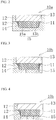
FIG. 2 is a schematic cross-sectional view of a first LED device inFIG. 1 taken along line II-II. -
FIG. 3 is a schematic cross-sectional view of a second LED device inFIG. 1 taken along line III-III. -
FIG. 4 is a schematic cross-section view of a variation of the second LED device. -
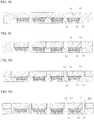
FIGS. 5A-5H each show a series of schematic cross-sectional views illustrating a method for manufacturing the first LED devices. -
FIGS. 6A-6H each show a series of schematic cross-sectional views illustrating a method for manufacturing the second LED devices. -
FIG. 7 is a schematic right side view of a variation of the LED module. - An embodiment of the present invention will be described below with reference to the accompanying drawings. It should be appreciated, however, that the embodiment described below is an illustration to give a concrete form to technical ideas of the present invention, and do not limit the present invention. In the explanations below, the same designations and reference numerals denote the same members or those of similar quality, for which the detailed explanations will be omitted when appropriate.
- In the
LED module 100 according to the present embodiment, as shown inFIG. 1 ,LED devices 10 are arranged on amounting board 20 in such a manner as to be adjacent to one another. TheLED devices 10 each has a lightemitting diode element 11, and areflective member 12 disposed along certain lateral surface of the lightemitting diode element 11. A first lighttransmissive member 13 is disposed above each lightemitting diode element 11. Here, the first lighttransmissive member 13 contains at least one phosphor. As shown inFIG. 1 andFIG. 2 , among all theLED devices 10, thefirst LED devices 10a have all of their lateral faces being adjacent to other LED devices, and have areflective member 12 disposed on all lateral faces of the first lighttransmissive members 13. The upper face of each of thefirst LED devices 10a serves as a light extraction face. On the other hand, as shown inFIG. 1 andFIG. 3 , thesecond LED devices 10b have those lateral faces that are adjacent to other LED devices and those that are not adjacent to other LED devices. Among all lateral faces of the first lighttransmissive members 13, those lateral faces that are adjacent to other LED devices are provided with thereflective member 12, and those lateral faces that are not adjacent to other LED devices are light extraction faces. As well as thefirst LED device 10a, the upper face of each of the second LED devices serves as a light extraction face. As shown inFIG. 1 , thesecond LED devices 10b are positioned along the outermost perimeter of theLED module 100, and thefirst LED devices 10a are positioned in the area other than the outermost perimeter of theLED module 100. Eachfirst LED device 10a is surrounded by other LED devices on all sides. Since the lateral faces of theLED module 100 serve as light extraction faces, theLED module 100 can have a wider light distribution as compared to an LED module having no light extraction faces serving as their lateral faces. In other words, because the light extraction faces of thesecond LED devices 10b are positioned at the lateral faces of theLED module 100, light can be laterally released from theLED module 100, and thus a wide light distribution can be achieved. - Furthermore, because all lateral faces of the first light
transmissive members 13 of thefirst LED devices 10a have thereflective member 12, the light emitted in thefirst LED devices 10a is reflected by thereflective members 12 and is extracted from the top of thefirst LED devices 10a. This can reduce the likelihood for the light emitted in thefirst LED devices 10a to be incident on and be absorbed by other LED devices. Similarly, because all of the lateral faces of the first lighttransmissive members 13 of thesecond LED devices 10b that are adjacent to other LED devices have thereflective member 12, the likelihood for the light to be incident on and be absorbed by other LED devices can be reduced. In addition, the likelihood of the light from thefirst LED devices 10a and thesecond LED devices 10b being incident on and being absorbed by themounting board 20 of theLED module 100 can also be reduced. Wherever thereflective members 12 are to be provided on the lateral faces of the first lighttransmissive members 13, thereflective members 12 are preferably disposed to entirely cover the lateral faces of the first lighttransmissive members 13. Although thesecond LED devices 10b have certain lateral faces serving as light extraction faces, these lateral faces are not adjacent to other LED devices. Thus, it is highly unlikely for the light to be incident on and be absorbed by other LED devices. As a result of all of the above, a decline of the light extraction efficiency of theLED module 100 can be moderated. - Furthermore, because the first light
transmissive members 13 of thefirst LED devices 10a and thesecond LED devices 10b have thereflective members 12 on the lateral faces that are adjacent to other LED devices, the paths traveled by light before being extracted from the top of theLED module 100 can be shortened as compared to the case of providing noreflective members 12. This can reduce the absorption of light by themounting board 20 or the like, thereby moderating the decline of the light extraction efficiency of theLED module 100. In other words, when there arereflective members 12 on the lateral faces of the first lighttransmissive members 13 of thefirst LED devices 10a and thesecond LED devices 10b, the light emitted in theLED devices 10 immediately hits thereflective members 12 and is extracted from the top of theLED devices 10. For this reason, the light can be extracted from the top of theLED module 100 before the light extraction efficiency declines. - As shown in
FIG. 2 and FIG. 3 , furthermore, disposingreflective members 12 on the lateral faces of the lightemitting diode elements 11 can reduce the likelihood for the light generated by the lightemitting diode elements 11 to be absorbed by the adjacent light emitting diode elements. The light generated at the emission layer of a lightemitting diode element 11 is more readily absorbed by the material, if the material composition of a component, on which the light hits, is more similar to the composition of the emission layer. Disposing thereflective members 12 can make it more difficult for the light to be absorbed by the emission layers of adjacent light emitting diode elements or their vicinities. Wherever thereflective members 12 are to be provided on the lateral faces of the lightemitting diode elements 11, thereflective members 12 are preferably disposed to cover the entire lateral faces of the lightemitting diode elements 11. - Each member of the
LED module 100 will be explained next. - The
LED devices 10 are preferably of a CSP-type (stands for "Chip Size Packages" or "Chip Scale Packages") wherereflective members 12 are disposed on the lateral faces of the lightemitting diode elements 11, rather than the type that provides a housing for each lightemitting diode element 11. In the case of a CSP-type LED device 10, areflective member 12 may also extend downwardly from a positions lateral to the light emitting diode element, and disposed under the lightemitting diode element 11. It is preferable for a CSP-type LED device to have metal terminals for external connection such as metal bumps or post electrodes for the n-side electrode 15a and the p-side electrode 15b. This allows for theLED devices 10 to be arranged closely to one another on the mountingboard 20. This increases the number of the LED devices that can be arranged on the mountingboard 20, thereby improving the luminous intensity of theLED module 100. By arranging theLED devices 10 close to one another, the emission face of theLED module 100 can emit light more uniformly when viewed from the top. When arranging the same number of theLED devices 10, arranging theLED devices 10 close to one another can also reduce the size of the mountingboard 20 thereby reducing the materials cost. Specifically, anLED device 10 can have a substantially rectangular shape of about 1 mm to about 2 mm per side as viewed from the top. Considering the mounting accuracy of theLED devices 10 arranged close to one another on the mountingboard 20, each distance between the light emittingdiode elements 11 is preferably in a range of about 0.4 mm to about 1.2 mm, and each distance between the LED devices is preferably about 0.2 mm to about 1 mm. - Preferably, the
LED devices 10 are arranged in a matrix when viewed from the top. This can make it easier to mount theLED devices 10 as well as making it easier to design the wiring pattern of the mountingboard 20 for mounting theLED devices 10. In addition, because theLED devices 10 are rectangular in shape when viewed from the top, they can be densely arranged to the outermost perimeter of the mountingboard 20. It is also preferable for theLED devices 10 to be serially connected. This can make the current values of theLED devices 10 substantially the same, and thus the light emitted from theLED devices 10 can be substantially uniform. Furthermore, as shown inFIG. 7 , theLED devices 10 are preferably arranged on both the upper face and the lower face of the mountingboard 20. This allows for theLED module 100 to emit light not only from the upper face but also from the lower face, and thus the light distribution of theLED module 100 can be further widened. - The
LED module 100 is produced by arranging the combination of thefirst LED devices 10a and thesecond LED devices 10b. Thefirst LED devices 10a and thesecond LED devices 10b can be produced, for example, by the method described below. In the explanation below, thesecond LED devices 10b are used by way of example. - As shown in
FIG. 5A , asupport substrate 30 is provided, and the light emittingdiode elements 11 are arranged on the upper face of thesupport substrate 30 with theelectrode 15 side up. Then, as shown inFIG. 5C , the light emittingdiode elements 11 and the surrounding of the light emittingdiode elements 11 are embedded with areflective member 12 so that theelectrodes 15 of the light emittingdiode elements 11 are exposed at the upper face of thereflective member 12. Thereflective member 12 is made of, for example, a white resin. Optionally, as shown inFIG. 5B , the secondlight transmissive member 14 described later may be disposed on the lateral faces of the light emittingdiode elements 11 prior to disposing thereflective member 12. Subsequently, as shown inFIG. 5D andFIG. 5E , thesupport substrate 30 is removed, and a firstlight transmissive member 13 is disposed in the area where thesupport substrate 30 has been removed. The firstlight transmissive member 13, for example, is a phosphor sheet. This provides the firstlight transmissive member 13 on the emission face side of the light emittingdiode elements 11. Subsequently, as shown inFIG. 5F and FIG. 5G , certain portions of the firstlight transmissive member 13 disposed on the emission face side of the light emittingdiode elements 11 are removed, and areflective member 12 is disposed in the removed areas. Then, as shown inFIG. 5H ,second LED devices 10b can be obtained by separating the light emittingdiode elements 11 into individual pieces by cutting the firstlight transmissive member 13 and thereflective member 12. - At this time, by partly removing the first
light transmissive member 13 and replacing it with areflective member 12 in such a manner as to surround two adjacent light emittingdiode elements 11 when viewed from the top, two pieces ofsecond LED devices 10b each having a light extraction face on one lateral face can be simultaneously obtained. Similarly, by partly removing the firstlight transmissive member 13 and replacing it with areflective member 12 in such a manner as to surround four adjacent light emittingdiode elements 11 when viewed from the top, four pieces ofsecond LED devices 10b each having two light extraction faces on two adjacent lateral surfaces can be simultaneously obtained. As shown inFIGS. 6A to 6H , thefirst LED devices 10a can be obtained using the similar method. In this case, by partly removing the firstlight transmissive member 13 and replacing it with thereflective member 12 in such a manner as to surround each of the light emittingdiode element 11 when viewed from the top, a piece offirst LED device 10a can be obtained. - As shown in
FIG. 5F andFIG. 6F , in partly removing the firstlight transmissive member 13, it is preferable to also partly remove thereflective member 12 in the vicinities of the areas where the firstlight transmissive member 13 and thereflective member 12 are in contact with one another. This can reduce the likelihood of allowing the portions of the firstlight transmissive member 13 that should be removed to remain unremoved. This can consequently reduce the likelihood of the light being released from the lateral faces of the firstlight transmissive members 13 of thefirst LED devices 10a and thesecond LED devices 10b that are adjacent to other LED devices. Moreover, the depths of removal of thereflective members 12 is preferably smaller than one half of the thickness of thereflective member 12. This allows for most of thereflective members 12 to remain, thereby maintaining the strength of theLED devices 10. - In partly removing the first
light transmissive member 13, moreover, it is preferable to not remove the secondlight transmissive members 14. This allows for the secondlight transmissive members 14 to maintain the oblique faces described later, and thus can more readily reflect the light from the light emittingdiode elements 11. - A semiconductor light emitting element can be used for the light emitting
diode element 11. The semiconductor light emitting element can include a light transmissive substrate and a semiconductor layer formed thereon. For the light transmissive substrate, for example, a light transmissive insulating material such as sapphire (Al2O3), or a semiconductor that can transmit the light emitted by the semiconductor layer, for example, a nitride-based semiconductor. The semiconductor layer includes, for example, a first conductivity type semiconductor layer (e.g., an n-type semiconductor layer), an emission layer, and a second conductivity type semiconductor layer (e.g., a p-type semiconductor layer). The semiconductor layer can be formed of a semiconductor material such as III-V Group compound semiconductor. Specifically, nitride-based semiconductors, such as InXAlYGa1-X-YN (0≤X, 0≤Y, X+Y≤1), for example, InN, AlN, GaN, InGaN, AlGaN, InGaAlN, or the like, can be used. - The
reflective member 12 can be formed using, for example, a metal layer or a white resin. Thereflective member 12 which is disposed on each lateral face of a light emittingdiode element 11 preferably has an oblique face on the light emittingdiode element 11 side such that the distance from the lateral face of the light emittingdiode element 11 to the oblique face increases as a distance from the mountingboard 20 to the oblique face increases. This allows the light from the light emittingdiode element 11 to hit the oblique face of thereflective member 12 to travel mainly towards the top. As a result, the light extraction efficiency of theLED device 10 can be increased as compared to the case of areflective member 12 without an oblique face. Moreover, forming the lateral faces of thereflective member 12 as curved faces can facilitate the reflection of the light from the light emittingdiode element 11 towards the top of theLED device 10, further increasing the light extraction efficiency of theLED device 10. - The second
light transmissive member 14 can be disposed between thereflective member 12 and the light emittingdiode element 11. This allows for the light from a light emittingdiode element 11 to be readily reflected by thereflective member 12. Examples of the materials for the secondlight transmissive member 14 include silicone resins, epoxy resins, and the like. The secondlight transmissive member 14 preferably has an oblique face on thereflective member 12 side such that the distance from the light emittingdiode element 11 to the oblique face increases as a distance from the mountingboard 20 to the oblique face increases. This makes it possible to form thereflective member 12 along the slant of the secondlight transmissive member 14. - The second
light transmissive member 14 having such a slant can be formed, for example, by the method described below. A light emittingdiode element 11 is placed on thesupport substrate 30 with theelectrode 15 side up. Then, in the case of using the secondlight transmissive member 14 formed of a light transmissive resin material, the liquid resin material which is the material for the secondlight transmissive member 14 is applied along the borders between the light emittingdiode element 11 and thesupport substrate 30 using a dispenser or the like. The liquid resin material spreads on thesupport substrate 30 while creeping on the lateral faces of the light emittingdiode element 11 due to surface tension. The liquid resin material is subsequently cured by heating or the like to obtain the secondlight transmissive member 14. This results in the slanted secondlight transmissive member 14. Thereflective member 12 can be formed in such a manner as to cover the oblique surfaces of such a secondlight transmissive member 14. - The distance of the liquid resin material creeping on the light emitting
diode element 11 can be controlled by adjusting the viscosity and the amount of the liquid resin material. The viscosity of the liquid resin material can be adjusted by adding a filler or the like. - The light extraction face of an
LED device 10 is constructed with a firstlight transmissive member 13. For example, the firstlight transmissive member 13 can be composed of a light transmissive material alone, or a light transmissive material which contains a phosphor. If the firstlight transmissive member 13 contains at least one phosphor, the light from the light emittingdiode element 11 can be converted, and the converted light can be extracted. The firstlight transmissive member 13 is preferably disposed to cover the entire path of light from the light emittingdiode element 11 to the light extraction face of theLED device 10. Furthermore, it is preferable that the light extraction face of theLED device 10 is formed of the firstlight transmissive member 13 in its entirety. In this manner, the light from the light emittingdiode element 11 can be extracted, and the light emittingdiode element 11 can be protected from the external factors. Moreover, the firstlight transmissive member 13 containing one or more phosphors and/or one or more scattering agents can reduce color non-uniformity of the light released from theLED device 10. As shown inFIG. 4 , it is preferable to dispose the firstlight transmissive member 13 on the lateral faces of the light emittingdiode element 11 of asecond LED device 10b that are not adjacent to anyother LED devices 10. In this manner, the light is also released from the lateral faces of the light emittingdiode elements 11, thereby further widening the light distribution of theLED module 100. Examples of materials for the light transmissive materials include light transmissive resins, glass, or the like. Examples of materials for the light transmissive resins include thermosetting resins such as silicone resins, silicone modified resins, epoxy resins, phenol resins, or the like, and thermoplastic resins such as polycarbonate resins, acrylic resins, methylpentene resins, polynorbornene resins or the like. Particularly, silicone resins are preferable due to its highly light resistant and heat resistant. - For phosphors, those that can be excited by the emitted light from the light emitting
diode elements 11 are used. Example of phosphors excitable by blue light or ultraviolet light include cerium-activated yttrium aluminum garnet-based phosphors; cerium-activated lutetium aluminum garnet-based phosphors; europium- and/or chromium-activated nitrogen-containing calcium aluminosilicate-based phosphors; europium-activated silicate-based phosphors; nitride-based phosphors, such as β-SiAlON phosphors, CASN-based phosphors, SCASN-based phosphors; KSF-based phosphors; sulfide-base phosphors; and quantum dot phosphors. By combining these phosphors with a blue light emittingdiode element 11 or an ultraviolet light emittingdiode element 11, LED devices of various emission colors (e.g., a white-based LED device 10) can be manufactured. The firstlight transmissive member 13 can contain various fillers for the purpose of, for example, adjusting the viscosity. In the case of using a silicone resin as the main material for the firstlight transmissive member 13, the firstlight transmissive member 13 may be covered with a coating film made of an epoxy resin having a low tack adhesive as the main material. - On the mounting
board 20,LED devices 10 are mounted. It is preferable to form a wiring pattern on the surface of the mountingboard 20 for supplying an electric current. By arranging theLED devices 10 on the wiring pattern and connecting theelectrodes 15 of theLED devices 10 to the wiring pattern using metal bumps, a conductive bonding agent, or the like, an electric current can be supplied to theLED devices 10. Specifically, an aluminum mounting board, copper mounting board, AlN mounting board, SiC mounting board, or the like can be used for the mountingboard 20.
Claims (15)
- An LED module comprising:a mounting board; anda plurality of LED devices arranged adjacent to one another on the mounting board, the LED devices includingat least one first LED device with all lateral faces facing corresponding ones of the plurality of LED devices, the at least one first LED device including a light emitting diode element, a light transmissive member disposed above the light emitting diode element, and a reflective member disposed lateral to the light emitting diode element with the reflective member further covering all lateral faces of the light transmissive member so that an upper face of the at least one first LED device serves as a light extraction face, anda plurality of second LED devices each having at least one lateral face facing at least one of the LED devices and at least one lateral face not facing any one of the LED devices, the second LED devices each including a light emitting diode element, a light transmissive member disposed above the light emitting diode element, and a reflective member disposed lateral to the light emitting diode element with the reflective member further covering each of at least one lateral face of the light transmissive member facing the at least one of the LED devices so that each of at least one lateral face of the light transmissive member not facing any one of the LED devices and an upper face of a corresponding one of the second LED devices serve as light extraction faces.
- The LED module according to claim 1, wherein
each of the reflective members disposed lateral to the light emitting diode element has an oblique face facing the light emitting diode element such that a distance from the light emitting diode element to the oblique face increases as a distance from the mounting board to the oblique face increases. - The LED module according to claim 2, wherein
the oblique face of each of the reflective members is curved. - The LED module according to any one of claims 1 to 3, wherein
each of the reflective members extends downwardly from a position lateral to the light emitting diode element, and is disposed under the light emitting diode element. - The LED module according to any one of claims 1 to 4, wherein
each of the reflective members includes white resin or a metal layer. - The LED module according to any one of claims 1 to 5, wherein
the light transmissive member is made of light transmissive resin or glass. - The LED module according to any one of claims 1 to 6, wherein
the light transmissive member contains at least one phosphor. - The LED module according to any one of claims 1 to 7, wherein
the light transmissive member covers an entire path of light from the light emitting diode element. - The LED module according to any one of claims 1 to 8, wherein
all of the light extraction faces are formed with the light transmissive member. - The LED module according to any one of claims 1 to 9, wherein
the light transmissive member of each of the second LED devices further covers at least one lateral face of the light emitting diode element on a side not facing any one of the LED devices. - The LED module according to any one of claims 1 to 10, wherein
each of the LED devices includes a second light transmissive member disposed between the reflective member and the light emitting diode element. - The LED module according to claim 11, wherein
the second light transmissive member is made of silicone resin or epoxy resin. - The LED module according to any one of claims 1 to 12, wherein
a distance between adjacent ones of the LED devices is in a range from 0.2 mm to 1 mm. - The LED module according to any one of claims 1 to 13, wherein
the LED devices are arranged in a matrix when viewed from the top, or serially connected. - The LED module according to any one of claims 1 to 14, wherein
the LED devices are disposed on an upper face and a lower face of the mounting board.
Applications Claiming Priority (2)
| Application Number | Priority Date | Filing Date | Title |
|---|---|---|---|
| JP2016129499 | 2016-06-30 | ||
| JP2017060500A JP6380590B2 (en) | 2016-06-30 | 2017-03-27 | LED module |
Publications (2)
| Publication Number | Publication Date |
|---|---|
| EP3264462A1 true EP3264462A1 (en) | 2018-01-03 |
| EP3264462B1 EP3264462B1 (en) | 2020-10-28 |
Family
ID=59296706
Family Applications (1)
| Application Number | Title | Priority Date | Filing Date |
|---|---|---|---|
| EP17179028.0A Active EP3264462B1 (en) | 2016-06-30 | 2017-06-30 | Led module |
Country Status (3)
| Country | Link |
|---|---|
| US (1) | US10641437B2 (en) |
| EP (1) | EP3264462B1 (en) |
| CN (1) | CN107565009B (en) |
Cited By (1)
| Publication number | Priority date | Publication date | Assignee | Title |
|---|---|---|---|---|
| WO2019165488A1 (en) * | 2018-03-02 | 2019-09-06 | A.B. Mikroelektronik Gesellschaft Mit Beschränkter Haftung | Chip scale package light emitting diode module for automotive lighting applications |
Families Citing this family (5)
| Publication number | Priority date | Publication date | Assignee | Title |
|---|---|---|---|---|
| US10641437B2 (en) | 2016-06-30 | 2020-05-05 | Nichia Corporation | LED module |
| CN110794614B (en) * | 2018-08-03 | 2022-10-25 | 日亚化学工业株式会社 | Light emitting module |
| JP6959548B2 (en) | 2018-10-04 | 2021-11-02 | 日亜化学工業株式会社 | Light emitting device and its manufacturing method |
| JP6947990B2 (en) | 2019-04-22 | 2021-10-13 | 日亜化学工業株式会社 | Manufacturing method of light emitting device and light emitting device |
| CN110970546B (en) * | 2019-12-19 | 2021-10-15 | 京东方科技集团股份有限公司 | Display substrate and manufacturing method thereof, and splicing display device |
Citations (5)
| Publication number | Priority date | Publication date | Assignee | Title |
|---|---|---|---|---|
| US20040218390A1 (en) * | 2003-01-24 | 2004-11-04 | Digital Optics International Corporation | High-density illumination system |
| US20070228392A1 (en) * | 2006-04-03 | 2007-10-04 | Ivoclar Vivadent Ag | Semiconductor radiation source and light curing device |
| JP2014143246A (en) | 2013-01-22 | 2014-08-07 | Citizen Electronics Co Ltd | LED module |
| EP2930749A1 (en) * | 2014-04-10 | 2015-10-14 | Stanley Electric Co., Ltd. | Light-emitting device and method of producing the same |
| EP2963685A1 (en) * | 2014-06-27 | 2016-01-06 | Nichia Corporation | Light emitting device |
Family Cites Families (17)
| Publication number | Priority date | Publication date | Assignee | Title |
|---|---|---|---|---|
| RU2503092C2 (en) * | 2008-09-25 | 2013-12-27 | Конинклейке Филипс Электроникс Н.В. | Coated light-emitting device and method of coating said device |
| US8506103B2 (en) * | 2008-11-26 | 2013-08-13 | Keiji Iimura | Semiconductor lamp and light bulb type LED lamp |
| CN101771025A (en) * | 2008-12-26 | 2010-07-07 | 富准精密工业(深圳)有限公司 | led |
| JP5810301B2 (en) | 2009-11-25 | 2015-11-11 | パナソニックIpマネジメント株式会社 | Lighting device |
| JP2011159812A (en) * | 2010-02-01 | 2011-08-18 | Panasonic Electric Works Co Ltd | Light emitting device |
| JP5745319B2 (en) * | 2011-04-14 | 2015-07-08 | 日東電工株式会社 | Fluorescent reflection sheet and method for manufacturing light emitting diode device |
| JP5341154B2 (en) | 2011-08-31 | 2013-11-13 | 株式会社フジクラ | High color rendering LED lamp unit |
| JP5829150B2 (en) | 2012-03-05 | 2015-12-09 | シチズンホールディングス株式会社 | Lighting device |
| JP6052952B2 (en) | 2012-03-22 | 2016-12-27 | 株式会社小糸製作所 | Light emitting module and vehicle lamp |
| US9810381B2 (en) | 2012-12-03 | 2017-11-07 | Citizen Watch Co., Ltd. | LED module |
| WO2014091914A1 (en) | 2012-12-10 | 2014-06-19 | シチズンホールディングス株式会社 | Led device and manufacturing method thereof |
| JP6258619B2 (en) | 2013-07-18 | 2018-01-10 | シチズン電子株式会社 | Lighting device |
| CN204289504U (en) * | 2014-07-18 | 2015-04-22 | 深圳市瑞丰光电子股份有限公司 | The encapsulating structure of wafer-level package LED |
| KR101607141B1 (en) * | 2014-08-20 | 2016-03-29 | 주식회사 루멘스 | Method for manufacturing light emitting device package |
| JP6515515B2 (en) | 2014-12-11 | 2019-05-22 | 日亜化学工業株式会社 | Manufacturing method of light emitting device |
| JP6380590B2 (en) | 2016-06-30 | 2018-08-29 | 日亜化学工業株式会社 | LED module |
| US10641437B2 (en) | 2016-06-30 | 2020-05-05 | Nichia Corporation | LED module |
-
2017
- 2017-06-29 US US15/636,804 patent/US10641437B2/en active Active
- 2017-06-30 CN CN201710522433.7A patent/CN107565009B/en active Active
- 2017-06-30 EP EP17179028.0A patent/EP3264462B1/en active Active
Patent Citations (5)
| Publication number | Priority date | Publication date | Assignee | Title |
|---|---|---|---|---|
| US20040218390A1 (en) * | 2003-01-24 | 2004-11-04 | Digital Optics International Corporation | High-density illumination system |
| US20070228392A1 (en) * | 2006-04-03 | 2007-10-04 | Ivoclar Vivadent Ag | Semiconductor radiation source and light curing device |
| JP2014143246A (en) | 2013-01-22 | 2014-08-07 | Citizen Electronics Co Ltd | LED module |
| EP2930749A1 (en) * | 2014-04-10 | 2015-10-14 | Stanley Electric Co., Ltd. | Light-emitting device and method of producing the same |
| EP2963685A1 (en) * | 2014-06-27 | 2016-01-06 | Nichia Corporation | Light emitting device |
Cited By (1)
| Publication number | Priority date | Publication date | Assignee | Title |
|---|---|---|---|---|
| WO2019165488A1 (en) * | 2018-03-02 | 2019-09-06 | A.B. Mikroelektronik Gesellschaft Mit Beschränkter Haftung | Chip scale package light emitting diode module for automotive lighting applications |
Also Published As
| Publication number | Publication date |
|---|---|
| CN107565009A (en) | 2018-01-09 |
| CN107565009B (en) | 2022-04-12 |
| US10641437B2 (en) | 2020-05-05 |
| US20180003349A1 (en) | 2018-01-04 |
| EP3264462B1 (en) | 2020-10-28 |
Similar Documents
| Publication | Publication Date | Title |
|---|---|---|
| US11791324B2 (en) | Light emitting device | |
| EP3264462B1 (en) | Led module | |
| JP6673410B2 (en) | LED module | |
| US10367129B2 (en) | Light emitting device | |
| US10141491B2 (en) | Method of manufacturing light emitting device | |
| JP6269702B2 (en) | Method for manufacturing light emitting device | |
| CN102237483B (en) | Light-emitting device | |
| JP6149487B2 (en) | LIGHT EMITTING DEVICE MANUFACTURING METHOD AND LIGHT EMITTING DEVICE | |
| US9431583B2 (en) | Semiconductor light emitting device | |
| US9022633B2 (en) | Linear light source device and planar light source device | |
| EP2811517A1 (en) | Semiconductor light emitting device | |
| CN107148684A (en) | light emitting device | |
| US20170018686A1 (en) | Method for manufacturing light emitting device | |
| JP4844246B2 (en) | Light emitting device and liquid crystal display backlight device | |
| US11227983B2 (en) | Light emitting device and method of manufacturing the light emitting device | |
| KR102470295B1 (en) | Light emitting device package |
Legal Events
| Date | Code | Title | Description |
|---|---|---|---|
| PUAI | Public reference made under article 153(3) epc to a published international application that has entered the european phase |
Free format text: ORIGINAL CODE: 0009012 |
|
| STAA | Information on the status of an ep patent application or granted ep patent |
Free format text: STATUS: THE APPLICATION HAS BEEN PUBLISHED |
|
| AK | Designated contracting states |
Kind code of ref document: A1 Designated state(s): AL AT BE BG CH CY CZ DE DK EE ES FI FR GB GR HR HU IE IS IT LI LT LU LV MC MK MT NL NO PL PT RO RS SE SI SK SM TR |
|
| AX | Request for extension of the european patent |
Extension state: BA ME |
|
| STAA | Information on the status of an ep patent application or granted ep patent |
Free format text: STATUS: REQUEST FOR EXAMINATION WAS MADE |
|
| 17P | Request for examination filed |
Effective date: 20180627 |
|
| RBV | Designated contracting states (corrected) |
Designated state(s): AL AT BE BG CH CY CZ DE DK EE ES FI FR GB GR HR HU IE IS IT LI LT LU LV MC MK MT NL NO PL PT RO RS SE SI SK SM TR |
|
| STAA | Information on the status of an ep patent application or granted ep patent |
Free format text: STATUS: EXAMINATION IS IN PROGRESS |
|
| 17Q | First examination report despatched |
Effective date: 20190702 |
|
| RIC1 | Information provided on ipc code assigned before grant |
Ipc: H01L 33/60 20100101ALN20200304BHEP Ipc: H01L 25/075 20060101AFI20200304BHEP |
|
| GRAP | Despatch of communication of intention to grant a patent |
Free format text: ORIGINAL CODE: EPIDOSNIGR1 |
|
| STAA | Information on the status of an ep patent application or granted ep patent |
Free format text: STATUS: GRANT OF PATENT IS INTENDED |
|
| INTG | Intention to grant announced |
Effective date: 20200420 |
|
| RIC1 | Information provided on ipc code assigned before grant |
Ipc: H01L 25/075 20060101AFI20200403BHEP Ipc: H01L 33/60 20100101ALN20200403BHEP |
|
| GRAS | Grant fee paid |
Free format text: ORIGINAL CODE: EPIDOSNIGR3 |
|
| GRAJ | Information related to disapproval of communication of intention to grant by the applicant or resumption of examination proceedings by the epo deleted |
Free format text: ORIGINAL CODE: EPIDOSDIGR1 |
|
| GRAL | Information related to payment of fee for publishing/printing deleted |
Free format text: ORIGINAL CODE: EPIDOSDIGR3 |
|
| STAA | Information on the status of an ep patent application or granted ep patent |
Free format text: STATUS: EXAMINATION IS IN PROGRESS |
|
| GRAR | Information related to intention to grant a patent recorded |
Free format text: ORIGINAL CODE: EPIDOSNIGR71 |
|
| STAA | Information on the status of an ep patent application or granted ep patent |
Free format text: STATUS: GRANT OF PATENT IS INTENDED |
|
| GRAA | (expected) grant |
Free format text: ORIGINAL CODE: 0009210 |
|
| STAA | Information on the status of an ep patent application or granted ep patent |
Free format text: STATUS: THE PATENT HAS BEEN GRANTED |
|
| INTC | Intention to grant announced (deleted) | ||
| RIC1 | Information provided on ipc code assigned before grant |
Ipc: H01L 25/075 20060101AFI20200907BHEP Ipc: H01L 33/60 20100101ALN20200907BHEP |
|
| AK | Designated contracting states |
Kind code of ref document: B1 Designated state(s): AL AT BE BG CH CY CZ DE DK EE ES FI FR GB GR HR HU IE IS IT LI LT LU LV MC MK MT NL NO PL PT RO RS SE SI SK SM TR |
|
| INTG | Intention to grant announced |
Effective date: 20200922 |
|
| REG | Reference to a national code |
Ref country code: GB Ref legal event code: FG4D |
|
| REG | Reference to a national code |
Ref country code: CH Ref legal event code: EP |
|
| REG | Reference to a national code |
Ref country code: AT Ref legal event code: REF Ref document number: 1329084 Country of ref document: AT Kind code of ref document: T Effective date: 20201115 |
|
| REG | Reference to a national code |
Ref country code: DE Ref legal event code: R096 Ref document number: 602017026193 Country of ref document: DE |
|
| REG | Reference to a national code |
Ref country code: IE Ref legal event code: FG4D |
|
| REG | Reference to a national code |
Ref country code: AT Ref legal event code: MK05 Ref document number: 1329084 Country of ref document: AT Kind code of ref document: T Effective date: 20201028 |
|
| REG | Reference to a national code |
Ref country code: NL Ref legal event code: MP Effective date: 20201028 |
|
| PG25 | Lapsed in a contracting state [announced via postgrant information from national office to epo] |
Ref country code: NO Free format text: LAPSE BECAUSE OF FAILURE TO SUBMIT A TRANSLATION OF THE DESCRIPTION OR TO PAY THE FEE WITHIN THE PRESCRIBED TIME-LIMIT Effective date: 20210128 Ref country code: NL Free format text: LAPSE BECAUSE OF FAILURE TO SUBMIT A TRANSLATION OF THE DESCRIPTION OR TO PAY THE FEE WITHIN THE PRESCRIBED TIME-LIMIT Effective date: 20201028 Ref country code: PT Free format text: LAPSE BECAUSE OF FAILURE TO SUBMIT A TRANSLATION OF THE DESCRIPTION OR TO PAY THE FEE WITHIN THE PRESCRIBED TIME-LIMIT Effective date: 20210301 Ref country code: RS Free format text: LAPSE BECAUSE OF FAILURE TO SUBMIT A TRANSLATION OF THE DESCRIPTION OR TO PAY THE FEE WITHIN THE PRESCRIBED TIME-LIMIT Effective date: 20201028 Ref country code: GR Free format text: LAPSE BECAUSE OF FAILURE TO SUBMIT A TRANSLATION OF THE DESCRIPTION OR TO PAY THE FEE WITHIN THE PRESCRIBED TIME-LIMIT Effective date: 20210129 Ref country code: FI Free format text: LAPSE BECAUSE OF FAILURE TO SUBMIT A TRANSLATION OF THE DESCRIPTION OR TO PAY THE FEE WITHIN THE PRESCRIBED TIME-LIMIT Effective date: 20201028 |
|
| REG | Reference to a national code |
Ref country code: LT Ref legal event code: MG4D |
|
| PG25 | Lapsed in a contracting state [announced via postgrant information from national office to epo] |
Ref country code: ES Free format text: LAPSE BECAUSE OF FAILURE TO SUBMIT A TRANSLATION OF THE DESCRIPTION OR TO PAY THE FEE WITHIN THE PRESCRIBED TIME-LIMIT Effective date: 20201028 Ref country code: AT Free format text: LAPSE BECAUSE OF FAILURE TO SUBMIT A TRANSLATION OF THE DESCRIPTION OR TO PAY THE FEE WITHIN THE PRESCRIBED TIME-LIMIT Effective date: 20201028 Ref country code: IS Free format text: LAPSE BECAUSE OF FAILURE TO SUBMIT A TRANSLATION OF THE DESCRIPTION OR TO PAY THE FEE WITHIN THE PRESCRIBED TIME-LIMIT Effective date: 20210228 Ref country code: PL Free format text: LAPSE BECAUSE OF FAILURE TO SUBMIT A TRANSLATION OF THE DESCRIPTION OR TO PAY THE FEE WITHIN THE PRESCRIBED TIME-LIMIT Effective date: 20201028 Ref country code: LV Free format text: LAPSE BECAUSE OF FAILURE TO SUBMIT A TRANSLATION OF THE DESCRIPTION OR TO PAY THE FEE WITHIN THE PRESCRIBED TIME-LIMIT Effective date: 20201028 Ref country code: BG Free format text: LAPSE BECAUSE OF FAILURE TO SUBMIT A TRANSLATION OF THE DESCRIPTION OR TO PAY THE FEE WITHIN THE PRESCRIBED TIME-LIMIT Effective date: 20210128 Ref country code: SE Free format text: LAPSE BECAUSE OF FAILURE TO SUBMIT A TRANSLATION OF THE DESCRIPTION OR TO PAY THE FEE WITHIN THE PRESCRIBED TIME-LIMIT Effective date: 20201028 |
|
| PG25 | Lapsed in a contracting state [announced via postgrant information from national office to epo] |
Ref country code: HR Free format text: LAPSE BECAUSE OF FAILURE TO SUBMIT A TRANSLATION OF THE DESCRIPTION OR TO PAY THE FEE WITHIN THE PRESCRIBED TIME-LIMIT Effective date: 20201028 |
|
| REG | Reference to a national code |
Ref country code: DE Ref legal event code: R097 Ref document number: 602017026193 Country of ref document: DE |
|
| PG25 | Lapsed in a contracting state [announced via postgrant information from national office to epo] |
Ref country code: SK Free format text: LAPSE BECAUSE OF FAILURE TO SUBMIT A TRANSLATION OF THE DESCRIPTION OR TO PAY THE FEE WITHIN THE PRESCRIBED TIME-LIMIT Effective date: 20201028 Ref country code: RO Free format text: LAPSE BECAUSE OF FAILURE TO SUBMIT A TRANSLATION OF THE DESCRIPTION OR TO PAY THE FEE WITHIN THE PRESCRIBED TIME-LIMIT Effective date: 20201028 Ref country code: CZ Free format text: LAPSE BECAUSE OF FAILURE TO SUBMIT A TRANSLATION OF THE DESCRIPTION OR TO PAY THE FEE WITHIN THE PRESCRIBED TIME-LIMIT Effective date: 20201028 Ref country code: EE Free format text: LAPSE BECAUSE OF FAILURE TO SUBMIT A TRANSLATION OF THE DESCRIPTION OR TO PAY THE FEE WITHIN THE PRESCRIBED TIME-LIMIT Effective date: 20201028 Ref country code: LT Free format text: LAPSE BECAUSE OF FAILURE TO SUBMIT A TRANSLATION OF THE DESCRIPTION OR TO PAY THE FEE WITHIN THE PRESCRIBED TIME-LIMIT Effective date: 20201028 Ref country code: SM Free format text: LAPSE BECAUSE OF FAILURE TO SUBMIT A TRANSLATION OF THE DESCRIPTION OR TO PAY THE FEE WITHIN THE PRESCRIBED TIME-LIMIT Effective date: 20201028 |
|
| PG25 | Lapsed in a contracting state [announced via postgrant information from national office to epo] |
Ref country code: DK Free format text: LAPSE BECAUSE OF FAILURE TO SUBMIT A TRANSLATION OF THE DESCRIPTION OR TO PAY THE FEE WITHIN THE PRESCRIBED TIME-LIMIT Effective date: 20201028 |
|
| PLBE | No opposition filed within time limit |
Free format text: ORIGINAL CODE: 0009261 |
|
| STAA | Information on the status of an ep patent application or granted ep patent |
Free format text: STATUS: NO OPPOSITION FILED WITHIN TIME LIMIT |
|
| 26N | No opposition filed |
Effective date: 20210729 |
|
| PG25 | Lapsed in a contracting state [announced via postgrant information from national office to epo] |
Ref country code: IT Free format text: LAPSE BECAUSE OF FAILURE TO SUBMIT A TRANSLATION OF THE DESCRIPTION OR TO PAY THE FEE WITHIN THE PRESCRIBED TIME-LIMIT Effective date: 20201028 Ref country code: AL Free format text: LAPSE BECAUSE OF FAILURE TO SUBMIT A TRANSLATION OF THE DESCRIPTION OR TO PAY THE FEE WITHIN THE PRESCRIBED TIME-LIMIT Effective date: 20201028 |
|
| PG25 | Lapsed in a contracting state [announced via postgrant information from national office to epo] |
Ref country code: SI Free format text: LAPSE BECAUSE OF FAILURE TO SUBMIT A TRANSLATION OF THE DESCRIPTION OR TO PAY THE FEE WITHIN THE PRESCRIBED TIME-LIMIT Effective date: 20201028 |
|
| PG25 | Lapsed in a contracting state [announced via postgrant information from national office to epo] |
Ref country code: MC Free format text: LAPSE BECAUSE OF FAILURE TO SUBMIT A TRANSLATION OF THE DESCRIPTION OR TO PAY THE FEE WITHIN THE PRESCRIBED TIME-LIMIT Effective date: 20201028 |
|
| REG | Reference to a national code |
Ref country code: CH Ref legal event code: PL |
|
| REG | Reference to a national code |
Ref country code: BE Ref legal event code: MM Effective date: 20210630 |
|
| PG25 | Lapsed in a contracting state [announced via postgrant information from national office to epo] |
Ref country code: LU Free format text: LAPSE BECAUSE OF NON-PAYMENT OF DUE FEES Effective date: 20210630 |
|
| PG25 | Lapsed in a contracting state [announced via postgrant information from national office to epo] |
Ref country code: LI Free format text: LAPSE BECAUSE OF NON-PAYMENT OF DUE FEES Effective date: 20210630 Ref country code: IE Free format text: LAPSE BECAUSE OF NON-PAYMENT OF DUE FEES Effective date: 20210630 Ref country code: CH Free format text: LAPSE BECAUSE OF NON-PAYMENT OF DUE FEES Effective date: 20210630 |
|
| PG25 | Lapsed in a contracting state [announced via postgrant information from national office to epo] |
Ref country code: IS Free format text: LAPSE BECAUSE OF FAILURE TO SUBMIT A TRANSLATION OF THE DESCRIPTION OR TO PAY THE FEE WITHIN THE PRESCRIBED TIME-LIMIT Effective date: 20210228 |
|
| PG25 | Lapsed in a contracting state [announced via postgrant information from national office to epo] |
Ref country code: BE Free format text: LAPSE BECAUSE OF NON-PAYMENT OF DUE FEES Effective date: 20210630 |
|
| PG25 | Lapsed in a contracting state [announced via postgrant information from national office to epo] |
Ref country code: HU Free format text: LAPSE BECAUSE OF FAILURE TO SUBMIT A TRANSLATION OF THE DESCRIPTION OR TO PAY THE FEE WITHIN THE PRESCRIBED TIME-LIMIT; INVALID AB INITIO Effective date: 20170630 |
|
| P01 | Opt-out of the competence of the unified patent court (upc) registered |
Effective date: 20230522 |
|
| PG25 | Lapsed in a contracting state [announced via postgrant information from national office to epo] |
Ref country code: CY Free format text: LAPSE BECAUSE OF FAILURE TO SUBMIT A TRANSLATION OF THE DESCRIPTION OR TO PAY THE FEE WITHIN THE PRESCRIBED TIME-LIMIT Effective date: 20201028 |
|
| PG25 | Lapsed in a contracting state [announced via postgrant information from national office to epo] |
Ref country code: MK Free format text: LAPSE BECAUSE OF FAILURE TO SUBMIT A TRANSLATION OF THE DESCRIPTION OR TO PAY THE FEE WITHIN THE PRESCRIBED TIME-LIMIT Effective date: 20201028 |
|
| PG25 | Lapsed in a contracting state [announced via postgrant information from national office to epo] |
Ref country code: MT Free format text: LAPSE BECAUSE OF FAILURE TO SUBMIT A TRANSLATION OF THE DESCRIPTION OR TO PAY THE FEE WITHIN THE PRESCRIBED TIME-LIMIT Effective date: 20201028 |
|
| REG | Reference to a national code |
Ref country code: DE Ref legal event code: R079 Ref document number: 602017026193 Country of ref document: DE Free format text: PREVIOUS MAIN CLASS: H01L0025075000 Ipc: H10H0029240000 |
|
| PGFP | Annual fee paid to national office [announced via postgrant information from national office to epo] |
Ref country code: DE Payment date: 20250507 Year of fee payment: 9 |
|
| PGFP | Annual fee paid to national office [announced via postgrant information from national office to epo] |
Ref country code: GB Payment date: 20250508 Year of fee payment: 9 |
|
| PGFP | Annual fee paid to national office [announced via postgrant information from national office to epo] |
Ref country code: FR Payment date: 20250508 Year of fee payment: 9 |
|
| PG25 | Lapsed in a contracting state [announced via postgrant information from national office to epo] |
Ref country code: TR Free format text: LAPSE BECAUSE OF FAILURE TO SUBMIT A TRANSLATION OF THE DESCRIPTION OR TO PAY THE FEE WITHIN THE PRESCRIBED TIME-LIMIT Effective date: 20201028 |