EP3258603B1 - Boucle à verrouillage de phase avec détecteur de verrouillage/déverrouillage - Google Patents
Boucle à verrouillage de phase avec détecteur de verrouillage/déverrouillage Download PDFInfo
- Publication number
- EP3258603B1 EP3258603B1 EP16174626.8A EP16174626A EP3258603B1 EP 3258603 B1 EP3258603 B1 EP 3258603B1 EP 16174626 A EP16174626 A EP 16174626A EP 3258603 B1 EP3258603 B1 EP 3258603B1
- Authority
- EP
- European Patent Office
- Prior art keywords
- signal
- phase
- lock
- locked loop
- detector
- Prior art date
- Legal status (The legal status is an assumption and is not a legal conclusion. Google has not performed a legal analysis and makes no representation as to the accuracy of the status listed.)
- Active
Links
- 230000004044 response Effects 0.000 claims description 8
- 230000003595 spectral effect Effects 0.000 claims description 6
- 238000001514 detection method Methods 0.000 description 5
- 238000010586 diagram Methods 0.000 description 5
- 230000007704 transition Effects 0.000 description 5
- 230000009471 action Effects 0.000 description 4
- 239000003990 capacitor Substances 0.000 description 4
- 238000000034 method Methods 0.000 description 4
- 230000003190 augmentative effect Effects 0.000 description 3
- 230000008859 change Effects 0.000 description 3
- 238000011084 recovery Methods 0.000 description 2
- 230000008901 benefit Effects 0.000 description 1
- 238000001914 filtration Methods 0.000 description 1
- 230000007935 neutral effect Effects 0.000 description 1
- 229920000729 poly(L-lysine) polymer Polymers 0.000 description 1
- 230000008569 process Effects 0.000 description 1
- 230000035945 sensitivity Effects 0.000 description 1
Images


Classifications
-
- H—ELECTRICITY
- H03—ELECTRONIC CIRCUITRY
- H03L—AUTOMATIC CONTROL, STARTING, SYNCHRONISATION, OR STABILISATION OF GENERATORS OF ELECTRONIC OSCILLATIONS OR PULSES
- H03L7/00—Automatic control of frequency or phase; Synchronisation
- H03L7/06—Automatic control of frequency or phase; Synchronisation using a reference signal applied to a frequency- or phase-locked loop
- H03L7/08—Details of the phase-locked loop
- H03L7/085—Details of the phase-locked loop concerning mainly the frequency- or phase-detection arrangement including the filtering or amplification of its output signal
- H03L7/095—Details of the phase-locked loop concerning mainly the frequency- or phase-detection arrangement including the filtering or amplification of its output signal using a lock detector
-
- H—ELECTRICITY
- H03—ELECTRONIC CIRCUITRY
- H03L—AUTOMATIC CONTROL, STARTING, SYNCHRONISATION, OR STABILISATION OF GENERATORS OF ELECTRONIC OSCILLATIONS OR PULSES
- H03L7/00—Automatic control of frequency or phase; Synchronisation
- H03L7/06—Automatic control of frequency or phase; Synchronisation using a reference signal applied to a frequency- or phase-locked loop
- H03L7/08—Details of the phase-locked loop
- H03L7/085—Details of the phase-locked loop concerning mainly the frequency- or phase-detection arrangement including the filtering or amplification of its output signal
- H03L7/091—Details of the phase-locked loop concerning mainly the frequency- or phase-detection arrangement including the filtering or amplification of its output signal the phase or frequency detector using a sampling device
-
- H—ELECTRICITY
- H03—ELECTRONIC CIRCUITRY
- H03L—AUTOMATIC CONTROL, STARTING, SYNCHRONISATION, OR STABILISATION OF GENERATORS OF ELECTRONIC OSCILLATIONS OR PULSES
- H03L7/00—Automatic control of frequency or phase; Synchronisation
- H03L7/06—Automatic control of frequency or phase; Synchronisation using a reference signal applied to a frequency- or phase-locked loop
- H03L7/08—Details of the phase-locked loop
- H03L7/099—Details of the phase-locked loop concerning mainly the controlled oscillator of the loop
- H03L7/0991—Details of the phase-locked loop concerning mainly the controlled oscillator of the loop the oscillator being a digital oscillator, e.g. composed of a fixed oscillator followed by a variable frequency divider
- H03L7/0992—Details of the phase-locked loop concerning mainly the controlled oscillator of the loop the oscillator being a digital oscillator, e.g. composed of a fixed oscillator followed by a variable frequency divider comprising a counter or a frequency divider
-
- H—ELECTRICITY
- H03—ELECTRONIC CIRCUITRY
- H03L—AUTOMATIC CONTROL, STARTING, SYNCHRONISATION, OR STABILISATION OF GENERATORS OF ELECTRONIC OSCILLATIONS OR PULSES
- H03L2207/00—Indexing scheme relating to automatic control of frequency or phase and to synchronisation
- H03L2207/50—All digital phase-locked loop
Definitions
- the present disclosure relates to a method of detecting lock and/or unlock in a phase locked loop, and a phase locked loop comprising a lock/unlock detector.
- Phase locked loops are used to generate an output signal with a defined phase and frequency relationship to an input reference signal.
- the output signal is matched to the phase of the input reference signal by a feedback loop in which the phase difference between the input reference signal and the output signal is determined by a phase detector.
- the phase detector In a digital phase locked loop, the phase detector outputs a digital signal.
- the output from the phase detector (indicating phase error) is received by a loop filter.
- the loop filter in turn provides an output signal to a frequency controlled oscillator.
- the phase detector may output a digital signal
- the loop filter may be a digital loop filter
- the frequency controlled oscillator may be a digitally controlled oscillator.
- Phase locked loops may operate in a linear mode, in which the phase detector provides a signal that varies in a linear relationship with the phase error.
- a phase locked loop may also operate in a "bang-bang" mode, in which the phase detector provides a binary signal, indicating only that the phase error is positive or negative.
- US 2005/123087 A1 discloses a circuit that detects erroneous phase lock occurring when the duty cycle of a data signal deviates from 100%.
- EP 1 885 067 discloses a phase lock loop (PLL) with a voltage controlled oscillator (VCO) for providing a VCO output signal.
- VCO voltage controlled oscillator
- a first phase/frequency detector for providing a first voltage tuning signal is included for controlling a frequency of the VCO output signal by comparing a first reference signal to the VCO output signal.
- a second phase/frequency detector for providing a second voltage tuning signal is included for controlling the frequency of the VCO output signal by comparing a second reference signal to the VCO output signal.
- EP1885067A2 discloses a phase lock loop (PLL) that includes a voltage controlled oscillator (VCO) for providing a VCO output signal.
- VCO voltage controlled oscillator
- a first phase/frequency detector (PFD) for providing a first voltage tuning signal (VT1) is included for controlling a frequency of the VCO output signal by comparing a first reference signal (f1) to the VCO output signal.
- a second phase/frequency detector (PFD) (110) for providing a second voltage tuning signal (VT2) is included for controlling the frequency of the VCO output signal by comparing a second reference signal to the VCO output signal.
- the first and second voltage tuning signals provide, respectively, first and second gains of frequency per volt for controlling the frequency of the VCO output signal.
- the first voltage tuning signal has a higher gain than the second voltage tuning signal.
- the first voltage tuning signal provides coarse frequency control of the VCO output signal and the second voltage tuning signal provides fine frequency control of the VCO output signal.
- US4423390A discloses a sidelock avoidance scheme for preventing sidelock in a PSK demodulator's carrier recovery loop that contains augmenting sweep control circuitry, including a frequency discriminator and an associated window comparator.
- the output of the frequency discriminator which is low pass filtered to remove noise, is applied to the window comparator which compares any differential between the true carrier and the output of a carrier recovery loop to a preset reference threshold representative of a frequency error condition that may approach sidelock.
- a preset reference threshold representative of a frequency error condition that may approach sidelock.
- an augmented frequency control voltage is applied to the voltage control oscillator of the loop to drive the oscillator away from a possible sidelock condition and toward the true carrier.
- the augmented frequency control voltage may be derived from a frequency sweep generator or from the output of the frequency discriminator, depending upon a selected strapping option.
- EP2797235A1 discloses a phase-locked loop device adapted for managing transition from relaxation-oscillation mode to random noise operation mode. It is designed for progressively reducing proportional (K P ) and integral (K I ) coefficients that are implemented in a loop filter of the PLL device. Recovering of last values formerly used for said proportional and integral coefficients is also provided, in case PLL lock state is lost. Such transition management may be combined with using a voltage-controlled oscillator within the PLL device, which has several control inputs.
- US2014/266355A1 discloses a method of operating a phase-locked loop (PLL) such as an all-digital PLL that includes operations of comparing a reference clock signal with a feedback signal of the PLL and outputting a comparison signal according to a result of the comparison, and detecting whether the PLL is in a lock state by using a number of times the comparison signal is toggled.
- PLL phase-locked loop
- JPS6098727A discloses detecting out of synchronism with high accuracy by converting digitally, amount of shift of synchronism between an input signal and an output signal into a pulse train, comparing the pulse train with a set value of a counter and outputting an out of synchronism display signal.
- US8081013B1 discloses a method for digital phase detection, comprises the steps of: providing a reference clock; receiving a feedback clock; determining a timing difference between the reference clock and the feedback clock; determining a polarity that indicates the leading or lagging relationship between the reference clock and the feedback clock; adaptively selecting one of at least two operating modes for generating a quantized level indicative of the timing difference, wherein in a first operating mode the quantized level is a constant maximum value and wherein in a second operating mode the quantized level is proportional to the timing difference; and generating a digital phase detection output as a combination of the polarity and the quantized level.
- US7388441B2 discloses a robust phase-lock detector for a phase-locked loop that examines both the sum frequency and baseband components of an error signal from the phase-locked loop to determine that both a reference signal and an output signal for the phase-locked loop are present and that the reference and output signals have a desired phase relationship.
- An IF detector selects the sum frequency component, which is the sum of the reference frequency and a subdivided frequency from the output signal, and detects its presence.
- a baseband detector selects the baseband component and detects whether the baseband component is approximately zero volts. The outputs from the IF detector and the baseband detector are combined to produce a lock signal, indicating that the phase-locked loop is locked, i.e., the reference and output signals are present and have the desired phase relationship with respect to each other.
- LO local oscillator
- phase locked loop comprising:
- the lock detector comprises a high pass filter configured to receive the phase error signal, and to pass high frequency content at the expected frequencies with which the bang-bang phase error will switch between its normalised limit values of +0.5 and -0.5 with a duty cycle of approximately 50% in phase lock and to attenuate lower frequencies associated with a settling phase of the phase locked loop.
- the lock detector comprises a rectifier for rectifying the output from the high pass filter to produce a rectified signal.
- the lock detector comprises a low pass filter arranged to receive a signal derived from the rectified signal.
- the lock detector may comprise a programmable gain element arranged to receive the rectified signal, and to provide a modified rectified signal to the low pass filter.
- the low pass filter and/or high pass filter may be configured such that a filter parameter of the low pass filter and/or the high pass filter can be varied using a control signal.
- the low pass filter may be configured to be reset in response to a signal indicating an unlock condition.
- the lock detector comprises an input enable device, configured not to pass the binary phase error signal when a signal indicating an unlock condition is present.
- the signal indicating an unlock condition may comprise at least one of: an indication that the phase locked loop is not in bang-bang mode, and an indication that the phase error signal has exceeded a predetermined threshold.
- the lock detector comprises a comparator configured to compare an output signal from the low pass filter with at least one threshold value, and to output a signal, derived from the comparison, that indicates a criterion for phase lock is met (or that criteria are met).
- the lock detector may comprise a timer, the timer configured to output a signal indicative of phase lock only when a signal, indicating a criterion for phase lock is met, has been in a predetermined state for a predetermined period.
- the lock detector may comprise a latch that is set by the signal from the timer, and reset by a signal that indicates an unlock condition.
- a receiver comprising the phase locked loop of any preceding claim.
- LO local oscillator
- PLL phase locked loop
- a locked state of a PLL generating a LO signal may be determined by identifying that the phase error is below a threshold that is sufficient to avoid lost symbols and date re-synchronization.
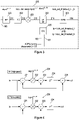
- FIG. 1 is a block diagram of an all-digital phase locked loop (ADPLL) 100.
- the phase locked loop 100 comprises: a reference phase generator 110, phase detector 104, loop filter 108, digitally controlled oscillator (DCO) 109, control block 105, lock detector 105, time to digital converter (TDC) 107, feedback divider 111, feedback register 112 and clock 103.
- DCO digitally controlled oscillator
- TDC time to digital converter
- the clock 103 is an optional part of the ADPLL 100, and provides a reference frequency signal 123 (e.g. 46.65MHz). In other embodiments the reference frequency 123 may simply be provided to the ADPLL 100 (e.g. by an external clock).
- the reference phase generator 110 comprises an adder 101 and register 102, arranged to integrate an input frequency control word FCW, and thereby provide a reference phase ramp ⁇ ref .
- a phase detector 104 compares the reference phase ramp ⁇ ref with a feedback ramp ⁇ fb derived from the output 127 of the DCO 109, and outputs a phase error signal ⁇ ⁇ .
- the feedback ramp ⁇ v is determined by combining (e.g. by fixed point concatenation) the output from the feedback register 112 and the TDC 107.
- the phase detector 104 is operable in a "bang-bang" mode, in which the output phase error signal ⁇ ⁇ is binary, either indicating a negative phase error or a positive phase error (e.g. -0.5 and +0.5 as normalised values respectively).
- the phase detector 104 may also be operable in a linear mode, in which the phase error signal ⁇ ⁇ is proportional to the phase error.
- the loop filter 108 receives the phase error signal ⁇ ⁇ , and performs a filtering operation.
- the loop filter 108 in this example is controlled by a control block 105, which may vary the configuration of the loop filter 108 (e.g. depending on the set FCW, and the loop state).
- the control block 105 may for example provide proportional gain k p and integral gain parameters k i to the loop filter 108 when in tracking mode.
- the loop filter 108 provides three output signals for controlling the DCO 109, these being a process voltage temperature control signal PVT, an acquisition control signal ACQ, and a tracking signal TR. Each of these control signals may control a different switched capacitor bank of the DCO 109, so as to vary the output frequency of the DCO 109.
- a frequency controlled oscillator may be used comprising a digital to analog converter and a varactor.
- the output from the DCO 109 is received by the feedback divider 111 and the TDC 107.
- the TDC 107 measures and quantizes the timing difference between transitions of the reference frequency 123 and the transitions of the ADPLL output signal 127.
- the feedback register 112 accumulates a count of the transitions in the frequency divided output of the ADPLL in each reference period.
- the output ⁇ f from the TDC 107 is combined with the output ⁇ i from the feedback register 112, for instance by concatenation.
- the output from the DCO 109 may have a frequency of around 4.5 GHz (e.g. 4.665 GHz).
- the PVT capacitor bank of the DCO 109 may have a tuning resolution of around 10 MHz
- the ACQ capacitor bank may have a tuning resolution of around 0.5 to 1 MHz
- the TR capacitor bank may have a tuning resolution on the order of 10 to 50 kHz.
- the TR mode may be able to handle a 1 MHz frequency offset.
- the control block 105 sequentially applies the correct loop filter parameters (e.g. k i and k p ) to the loop filter 108 so that first the PVT output, then the ACQ output, and finally the TR output can settle.
- the lock sequence starts with a PVT mode in which the loop filter 108 generates the PVT control signal, with the ACQ and TR control signals set to a neutral value (e.g. 0, where the ACQ and TR signals can be positive and negative).
- the PVT control signal is frozen, and the loop continues in ACQ mode.
- the ACQ mode is accomplished, the ACQ word is frozen and the loop enters TR mode.
- the phase detector 104 may operate in a linear mode. When the loop enters TR mode, the phase detector 104 switches to a bang-bang mode of operation (as described above).
- the loop filter 108 may be configured (e.g. in response to a control signal from the control block 105) to change the TR output by a small and constant increment (positive or negative) for each clock cycle that there is a (positive or negative) phase error.
- a settling period (e.g. with some ringing) may occur when the loop filter 108 is switched to bang-bang mode.
- the ADPLL is not tuning between two states of the phase detector 104 (as in linear mode), but instead around a state (i.e. zero phase error). This means that the phase modulation is smaller than in linear mode, and hence the in-band phase noise performance is considerably better in bang-bang mode than in linear mode.
- the phase locked loop 100 further comprises a lock detector 150, configured to determine when the ADPLL 100 is locked and unlocked.
- the lock detector 150 is shown in more detail in figure 2 , and comprises: input enable switch 151, detector core 200, timer 154, latch 155, and logic and comparator blocks 153, 152, 156, 157.
- the input enable switch 151 passes through the phase error 125 to the rest of the lock detector 150, unless the logic gate 152 indicates that the ADPLL is not in bang-bang mode, in which case a null signal '0' is provided.
- the logic gate 152 receives a TR signal 162, which indicates (e.g. is high) when the ADPLL 100 is not in TR mode, and a
- the logic gate 152 is an OR gate, but other arrangements are possible.
- the output from the logic gate 152 indicates when the ADPLL 100 is not in TR mode, and if the phase error ⁇ ⁇ is outside the bang-bang range of +/- 0.5.
- the output signal 163 from the input enable switch 151 is therefore zero if the ADPLL is not in TR mode and if the phase error is outside +/-0.5.
- the detector core 200 receives the output from the input enable switch 151 and determines whether the spectral characteristics and/or duty cycle of the phase error is indicative of phase lock.
- the phase error will comprise a high frequency signal with a duty cycle of approximately 50%. Either or both of these criteria may be detected by the detector core 200 to indicate phase lock in bang-bang mode.
- the detector core 200 comprises a high pass (HP) filter 220, rectifier 202, gain block 203, low pass (LP) filter 230 and comparator 205.
- HP high pass
- LP low pass
- the HP filter 220 passes high frequency content (e.g. at the expected frequency with which the bang-bang phase error will switch between +/-0.5 in phase lock) and attenuates lower frequencies (associated with a settling phase).
- FIG. 4 An example of a suitable architecture for the HP filter 220 is shown in figure 4 , and comprises a first summing block 221, gain block 222, second summing block 223, unit delay 224 and third summing block 225.
- the first summing block 221 subtracts the output of the unit delay 224 from the input signal 163.
- the gain block 222 receives the output from the first summing block 221, and multiplies this by a programmable gain factor khp, which may be equal to 2 0...-8 (i.e. may be selectable in the range 2° to 2 -8 ).
- the second summing block 223 adds the output from the gain block 222 to the output of the unit delay 224.
- the unit delay operates on the output from the second summing block 223.
- the third summing block 225 subtracts the input signal 163 from the output of the unit delay block 224, to produce the edge signal 211.
- Other arrangements are possible for the HP filter 220.
- the rectifier 202 receives the HP filtered signal 211 from the HP filter 220, and rectifies it, and provides a rectified signal 212 to the programmable gain block 203.
- the gain block 203 multiplies the rectified signal 212 by a programmable lock sensitivity factor, lock_det_sensitivity (e.g. 2 0...7 ), to produce an input signal 213 for the low pass filter 230.
- lock_det_sensitivity e.g. 2 0...7
- FIG 4 An example architecture for the LP filter 230 is shown in figure 4 , comprising a first order infinite impulse response (IIR) filter. Any architecture that produces a low pass frequency response may be used, e.g. moving average, etc.
- the forward path of the low pass filter 230 of figure 4 comprises (in order) a first summing block 231, multiplier 232, second summing block 233 and unit delay 234.
- the output from the unit delay 234 is fed-back to the first summing block 231, where it is subtracted from the input signal to the filter 230, and to the second summing block 233, where it is added to the output of the multiplier 232.
- the multiplier 232 applies a gain factor (kip) to the output of the first summing block 233, and passes the result to the second summing block 233.
- the gain factor klp may be selectable in the range 2° to 2 -15 .
- the low pass filter 230 may be reset in response to a reset signal (rst).
- the reset signal rst is provided by logic gate 206.
- the inputs to logic gate 206 are the TR signal 162 and the
- the LP filtered signal 214 from the LP filter 230 is provided to a comparator 205 that determines whether the LP filtered signal 214 has met a predetermined threshold condition (indicative of lock).
- the comparator 205 provides an output signal that indicates when the filtered signal (Ip) is within an envelope defined by a low threshold (lock_det_threshold_l) and a high threshold (lock_det_threshold_h), i.e.
- the comparator output signal 164 indicates this (e.g. by going high).
- a single threshold may be used, and an output provided when this is exceeded.
- the present example has a low threshold of around 0.2, and a high threshold of around 0.4 (normalised values compared with 0.25 for a bang-bang ADPLL in which the phase error is varying between -0.5 and +0.5 with a duty cycle of 50%).
- the output 164 from the detector core 200 is a signal that indicates that the spectral content and/or duty cycle of the phase error 125 meets a criterion (or criteria) indicative of phase lock in bang-bang mode.
- the HP filter 220 may, in some examples, be replaced by an edge detector.
- the detector core 200 may comprise counters that detect and count high and low events of the phase error 125. In those examples, the count of high and low within an interval can be compared and if they are sufficiently similar, that may indicate phase lock. The count results may be filtered to avoid false detection of phase lock.
- One advantage of the embodiment of figure 3 is flexibility: it can be adjusted (e.g. by varying parameters) to suit a wide range of applications.
- the timer 154 and latch 155 are optional features of the lock detector 150 that improve the reliability of lock indication, helping to prevent false indications of lock.
- the timer 154 is configured to provide an output that indicates whether the detector core 200 output signal 164 has indicated lock for a predetermined threshold period.
- the latch 155 is set by the timer output signal 165, and reset in response to: the detector core 200 criterion (or criteria) not being met (indicated by the output from the inverter 156); a TR signal 162; or a
- the output 166 from the latch 156 is the lock detection signal, and reliably indicates whether lock has been achieved. Furthermore, it will may also rapidly indicate that when unlock occurs.
- Figure 5 illustrates the operation of the example embodiment of figures 1 to 4 , showing a time history of: phase error 125, edge/zero crossing output 211, rectifier output signal 212, low pass filter output signal 214, comparator output signal 164 (indicating the lock criterion is met), and the latch output 166.
- the input enable switch 151 prevents the lock detector 150 receiving any phase error signals, so there is no potential for a false lock indication during this period.
- the ADPLL enters TR mode there is some ringing of the loop filter 108 before it settles.
- the amplitude of the phase error 125 is generally greater than 0.5, so the input enable switch 151 does not generally pass any signal to the detector core 200.
- the ringing of the loop filter 108 generates some non-zero output values from the high pass filter 220 (as it crosses zero), but these are of very short duration, and subsequently do not result in a significant change in the low pass filter output signal 214.
- the phase error has largely settled to within the bang-bang limits of +/-0.5, but comprises largely low frequency spectral content, which does not result in a consistent response from the HP filter 220.
- the phase error starts to vary between -0.5 and +0.5 with a duty cycle of approximately 50%, at high frequency, and this phase error signal 125 is passed through the HP filter 220 and the rectifier 202.
- the LP filter 230 consequently receives a signal with a DC component, resulting in significant change in the LP filter output signal 214.
- the LP output signal 214 is within the envelope criteria of the comparator 205.
- the comparator output signal 164 consequently goes high, to indicate that the lock criteria are currently met. This high signal triggers the timer 154, which latches the lock detector output 126 after the output signal 126 has indicated that the lock criteria 251, 252 have been met for a predetermined period, at t ⁇ 0.55ms.
- the timer can be reset by logic 157 if conditions indicating unlock occur.
- One application for a PLL according to the invention may be a communications device, such as a satellite or AM/FM radio receiver.
- a further application may be a radar chirp generator, e.g. for use in a vehicle proximity detector.
Claims (8)
- Boucle à verrouillage de phase (100) comprenant :un détecteur de phase (104), utilisable dans un mode tout ou rien pour fournir un signal d'erreur de phase binaire (Δϕ) indiquant qu'il y a une différence de phase soit positive soit négative entre un signal de référence (ϕref) et un signal de rétroaction (ϕfb) ;un filtre de boucle (108) configuré pour fournir un signal de commande (TR) dérivé du signal d'erreur de phase binaire ;un oscillateur commandé en fréquence (109) configuré pour recevoir le signal de commande et fournir un signal de sortie (127) avec une fréquence qui varie en fonction du signal de commande ; etun détecteur de verrouillage/déverrouillage (150) configuré pour déterminer un état de verrouillage/déverrouillage de la boucle à verrouillage de phase, l'état de verrouillage/déverrouillage étant dérivé de caractéristiques spectrales du signal d'erreur de phase binaire et/ou d'un rapport cyclique du signal d'erreur de phase binaire.caractérisée en ce quele détecteur de verrouillage (150) comprend :un filtre passe-haut (220) configuré pour recevoir le signal d'erreur de phase, et pour laisser passer du contenu haute fréquence aux fréquences prévues avec lesquelles l'erreur de phase en tout ou rien commutera entre ses valeurs limites normalisées de +0,5 et -0,5 avec un rapport cyclique d'environ 50 % en verrouillage de phase et pour atténuer des fréquences plus basses associées à une phase de stabilisation de la boucle à verrouillage de phase (100) ;un redresseur (202) pour redresser la sortie du filtre passe-haut (220) pour produire un signal redressé (212) ;un filtre passe-bas (230) agencé pour recevoir un signal (213) dérivé du signal redressé ;un comparateur (205) configuré pour comparer un signal de sortie du filtre passe-bas (230) avec au moins une valeur seuil, et pour délivrer un signal (164), dérivé de la comparaison, qui indique qu'au moins un critère pour le verrouillage de phase est satisfait ; etun dispositif d'activation d'entrée (151), configuré pour ne pas laisser passer le signal d'erreur de phase binaire lorsqu'un signal indiquant une condition de déverrouillage est présent.
- Boucle à verrouillage de phase (100) selon la revendication 1, le détecteur de verrouillage (150) comprenant un élément à gain programmable (203) agencé pour recevoir le signal redressé (212), et pour fournir un signal redressé modifié (213) au filtre passe-bas (230) le signal redressé modifié étant le résultat de la multiplication entre le signal redressé (213) et le facteur de gain programmable.
- Boucle à verrouillage de phase (100) selon la revendication 1 ou 2, un paramètre de filtre du filtre passe-bas (230) et/ou du filtre passe-haut (220) étant variable en utilisant un signal de commande.
- Boucle à verrouillage de phase (100) selon l'une quelconque des revendications 1 à 3, le filtre passe-bas (230) étant configuré pour être réinitialisé en réponse à un signal (rst) indiquant une condition de déverrouillage.
- Boucle à verrouillage de phase (100) selon l'une quelconque des revendications précédentes, le signal indiquant une condition de déverrouillage comprenant au moins une parmi : une indication que la boucle à verrouillage de phase (100) n'est pas en mode tout ou rien, et une indication que le signal d'erreur de phase a dépassé un seuil prédéterminé.
- Boucle à verrouillage de phase (100) selon l'une quelconque des revendications précédentes, le détecteur de verrouillage (150) comprenant un temporisateur (154), le temporisateur (154) étant configuré pour délivrer un signal (165) indiquant le verrouillage de phase uniquement lorsqu'un signal (164), indiquant qu'au moins un critère pour le verrouillage de phase est satisfait, a été dans un état prédéterminé pendant une période prédéterminée.
- Boucle à verrouillage de phase (100) selon la revendication 6, le détecteur de verrouillage (150) comprenant un verrou (155) qui est initialisé par le signal (165) provenant du temporisateur (154), et réinitialisé par un signal (156) qui indique une condition de déverrouillage.
- Récepteur comprenant la boucle à verrouillage de phase (100) selon l'une quelconque des revendications précédentes.
Priority Applications (4)
| Application Number | Priority Date | Filing Date | Title |
|---|---|---|---|
| EP16174626.8A EP3258603B1 (fr) | 2016-06-15 | 2016-06-15 | Boucle à verrouillage de phase avec détecteur de verrouillage/déverrouillage |
| JP2017104410A JP2017225113A (ja) | 2016-06-15 | 2017-05-26 | ロック/アンロック検出器を有する位相ロックループ |
| US15/609,935 US10187069B2 (en) | 2016-06-15 | 2017-05-31 | Phase locked loop with lock/unlock detector |
| CN201710416144.9A CN107528586B (zh) | 2016-06-15 | 2017-06-05 | 具有锁定/解锁检测器的锁相回路 |
Applications Claiming Priority (1)
| Application Number | Priority Date | Filing Date | Title |
|---|---|---|---|
| EP16174626.8A EP3258603B1 (fr) | 2016-06-15 | 2016-06-15 | Boucle à verrouillage de phase avec détecteur de verrouillage/déverrouillage |
Publications (2)
| Publication Number | Publication Date |
|---|---|
| EP3258603A1 EP3258603A1 (fr) | 2017-12-20 |
| EP3258603B1 true EP3258603B1 (fr) | 2022-11-09 |
Family
ID=56131469
Family Applications (1)
| Application Number | Title | Priority Date | Filing Date |
|---|---|---|---|
| EP16174626.8A Active EP3258603B1 (fr) | 2016-06-15 | 2016-06-15 | Boucle à verrouillage de phase avec détecteur de verrouillage/déverrouillage |
Country Status (4)
| Country | Link |
|---|---|
| US (1) | US10187069B2 (fr) |
| EP (1) | EP3258603B1 (fr) |
| JP (1) | JP2017225113A (fr) |
| CN (1) | CN107528586B (fr) |
Families Citing this family (6)
| Publication number | Priority date | Publication date | Assignee | Title |
|---|---|---|---|---|
| US10305493B2 (en) * | 2014-10-22 | 2019-05-28 | Sony Semiconductor Solutions Corporation | Phase-locked loop and frequency synthesizer |
| US10164646B1 (en) * | 2017-07-28 | 2018-12-25 | Taiwan Semiconductor Manufacturing Company Ltd. | Frequency generator with warning mechanism |
| DE112018008073B4 (de) * | 2018-11-20 | 2022-08-11 | Mitsubishi Electric Corporation | Einrasterfassungsschaltung und Phasenregelschleifenschaltung |
| US10778233B1 (en) | 2019-08-14 | 2020-09-15 | Nxp B.V. | Phase locked loop with phase and frequency lock detection |
| US11271572B2 (en) * | 2020-04-29 | 2022-03-08 | Analog Devices International Unlimited Company | Self-tuning phase-locked loop (PLL) circuit |
| US11817869B2 (en) * | 2022-03-16 | 2023-11-14 | Nxp B.V. | System and method of controlling frequency of a digitally controlled oscillator with temperature compensation |
Citations (7)
| Publication number | Priority date | Publication date | Assignee | Title |
|---|---|---|---|---|
| US4423390A (en) * | 1981-01-09 | 1983-12-27 | Harris Corporation | Side lock avoidance network for PSK demodulator |
| JPS6098727A (ja) * | 1983-11-04 | 1985-06-01 | Mitsubishi Electric Corp | 同期はずれ検出回路 |
| EP1885067A2 (fr) * | 2006-07-13 | 2008-02-06 | Itt Manufacturing Enterprises, Inc. | Boucle à verrouillage de phase de faible bruit avec détecteur de verrouillage de haute précision |
| US7388441B2 (en) * | 2006-05-23 | 2008-06-17 | Tektronix. Inc. | Robust phase-lock detector |
| US8081013B1 (en) * | 2010-07-13 | 2011-12-20 | Amlogic Co., Ltd. | Digital phase and frequency detector |
| US20140266355A1 (en) * | 2013-03-13 | 2014-09-18 | Jae Jin Park | Phase-locked loop, method of operating the same, and devices having the same |
| EP2797235A1 (fr) * | 2013-04-22 | 2014-10-29 | Asahi Kasei Microdevices Corporation | Dispositif de boucle à phase asservie avec transition gérée de mode de fonctionnement de bruit aléatoire |
Family Cites Families (5)
| Publication number | Priority date | Publication date | Assignee | Title |
|---|---|---|---|---|
| JP3926368B2 (ja) * | 2002-12-11 | 2007-06-06 | 富士通株式会社 | 位相誤同期検出回路 |
| US7592847B2 (en) * | 2007-03-22 | 2009-09-22 | Mediatek Inc. | Phase frequency detector and phase-locked loop |
| DE102009012440A1 (de) * | 2009-03-11 | 2010-09-23 | Rohde & Schwarz Gmbh & Co. Kg | Phasenregelschleife und Verfahren zum Ermitteln eines Einrastzustandes einer Phasenregelschleife |
| US20140354262A1 (en) | 2013-06-03 | 2014-12-04 | Qualcomm Incorporated | Lock detector for digital phase-locked loop |
| EP3096460B1 (fr) | 2015-05-20 | 2019-11-06 | Nxp B.V. | Boucle à verrouillage de phase avec détecteur de verrouillage |
-
2016
- 2016-06-15 EP EP16174626.8A patent/EP3258603B1/fr active Active
-
2017
- 2017-05-26 JP JP2017104410A patent/JP2017225113A/ja active Pending
- 2017-05-31 US US15/609,935 patent/US10187069B2/en active Active
- 2017-06-05 CN CN201710416144.9A patent/CN107528586B/zh active Active
Patent Citations (7)
| Publication number | Priority date | Publication date | Assignee | Title |
|---|---|---|---|---|
| US4423390A (en) * | 1981-01-09 | 1983-12-27 | Harris Corporation | Side lock avoidance network for PSK demodulator |
| JPS6098727A (ja) * | 1983-11-04 | 1985-06-01 | Mitsubishi Electric Corp | 同期はずれ検出回路 |
| US7388441B2 (en) * | 2006-05-23 | 2008-06-17 | Tektronix. Inc. | Robust phase-lock detector |
| EP1885067A2 (fr) * | 2006-07-13 | 2008-02-06 | Itt Manufacturing Enterprises, Inc. | Boucle à verrouillage de phase de faible bruit avec détecteur de verrouillage de haute précision |
| US8081013B1 (en) * | 2010-07-13 | 2011-12-20 | Amlogic Co., Ltd. | Digital phase and frequency detector |
| US20140266355A1 (en) * | 2013-03-13 | 2014-09-18 | Jae Jin Park | Phase-locked loop, method of operating the same, and devices having the same |
| EP2797235A1 (fr) * | 2013-04-22 | 2014-10-29 | Asahi Kasei Microdevices Corporation | Dispositif de boucle à phase asservie avec transition gérée de mode de fonctionnement de bruit aléatoire |
Also Published As
| Publication number | Publication date |
|---|---|
| JP2017225113A (ja) | 2017-12-21 |
| EP3258603A1 (fr) | 2017-12-20 |
| CN107528586B (zh) | 2024-02-23 |
| US20170366192A1 (en) | 2017-12-21 |
| CN107528586A (zh) | 2017-12-29 |
| US10187069B2 (en) | 2019-01-22 |
Similar Documents
| Publication | Publication Date | Title |
|---|---|---|
| EP3258603B1 (fr) | Boucle à verrouillage de phase avec détecteur de verrouillage/déverrouillage | |
| US9614536B2 (en) | Phase locked loop with lock detector | |
| US9838024B2 (en) | Auto frequency calibration method | |
| CN106341122B (zh) | 具有多频段振荡器的锁相环以及校准其的方法 | |
| US6320469B1 (en) | Lock detector for phase-locked loop | |
| US7323940B2 (en) | Adaptive cycle-slipped detector for unlock detection in phase-locked loop applications | |
| US7956658B2 (en) | Digital lock detector and frequency synthesizer using the same | |
| US8644783B2 (en) | Methods and systems for determining an offset term for a synthesizer signal, and methods and systems for producing a phase-corrected digital signal | |
| US5015971A (en) | Frequency agile microwave signal generator | |
| CN111697967B (zh) | 一种自适应数字化驯服时钟的系统 | |
| US20020090045A1 (en) | Digital clock recovery system | |
| US6753711B2 (en) | Digital summing phase-lock loop circuit with sideband control and method therefor | |
| US7646227B2 (en) | Digital phase discriminator | |
| US6362693B2 (en) | Frequency detection method for adjusting a clock signal frequency and a frequency detector circuit for carrying out the method | |
| US7598816B2 (en) | Phase lock loop circuit with delaying phase frequency comparson output signals | |
| US6965660B2 (en) | Digital phase-locked loop | |
| JP5872949B2 (ja) | Pll周波数シンセサイザ、半導体集積装置及び無線通信機器 | |
| US6087902A (en) | Phase-locked loop (PLL) circuit containing a biased phase detector for improved frequency acquisition | |
| US6160860A (en) | Phase-locked loop (PLL) circuit containing a frequency detector for improved frequency acquisition | |
| Martirosov et al. | Additive high-speed synchronization techniques in pll systems | |
| KR100459760B1 (ko) | 디지털텔레비젼수신장치의자동이득제어회로및방법 | |
| US20020168028A1 (en) | Frequency-modulated signal receiver with digital demodulator |
Legal Events
| Date | Code | Title | Description |
|---|---|---|---|
| PUAI | Public reference made under article 153(3) epc to a published international application that has entered the european phase |
Free format text: ORIGINAL CODE: 0009012 |
|
| STAA | Information on the status of an ep patent application or granted ep patent |
Free format text: STATUS: THE APPLICATION HAS BEEN PUBLISHED |
|
| AK | Designated contracting states |
Kind code of ref document: A1 Designated state(s): AL AT BE BG CH CY CZ DE DK EE ES FI FR GB GR HR HU IE IS IT LI LT LU LV MC MK MT NL NO PL PT RO RS SE SI SK SM TR |
|
| AX | Request for extension of the european patent |
Extension state: BA ME |
|
| STAA | Information on the status of an ep patent application or granted ep patent |
Free format text: STATUS: REQUEST FOR EXAMINATION WAS MADE |
|
| STAA | Information on the status of an ep patent application or granted ep patent |
Free format text: STATUS: EXAMINATION IS IN PROGRESS |
|
| 17P | Request for examination filed |
Effective date: 20180620 |
|
| RBV | Designated contracting states (corrected) |
Designated state(s): AL AT BE BG CH CY CZ DE DK EE ES FI FR GB GR HR HU IE IS IT LI LT LU LV MC MK MT NL NO PL PT RO RS SE SI SK SM TR |
|
| 17Q | First examination report despatched |
Effective date: 20180719 |
|
| STAA | Information on the status of an ep patent application or granted ep patent |
Free format text: STATUS: EXAMINATION IS IN PROGRESS |
|
| STAA | Information on the status of an ep patent application or granted ep patent |
Free format text: STATUS: EXAMINATION IS IN PROGRESS |
|
| GRAP | Despatch of communication of intention to grant a patent |
Free format text: ORIGINAL CODE: EPIDOSNIGR1 |
|
| STAA | Information on the status of an ep patent application or granted ep patent |
Free format text: STATUS: GRANT OF PATENT IS INTENDED |
|
| INTG | Intention to grant announced |
Effective date: 20220802 |
|
| GRAS | Grant fee paid |
Free format text: ORIGINAL CODE: EPIDOSNIGR3 |
|
| GRAA | (expected) grant |
Free format text: ORIGINAL CODE: 0009210 |
|
| STAA | Information on the status of an ep patent application or granted ep patent |
Free format text: STATUS: THE PATENT HAS BEEN GRANTED |
|
| AK | Designated contracting states |
Kind code of ref document: B1 Designated state(s): AL AT BE BG CH CY CZ DE DK EE ES FI FR GB GR HR HU IE IS IT LI LT LU LV MC MK MT NL NO PL PT RO RS SE SI SK SM TR |
|
| REG | Reference to a national code |
Ref country code: GB Ref legal event code: FG4D |
|
| REG | Reference to a national code |
Ref country code: CH Ref legal event code: EP Ref country code: AT Ref legal event code: REF Ref document number: 1531030 Country of ref document: AT Kind code of ref document: T Effective date: 20221115 |
|
| REG | Reference to a national code |
Ref country code: DE Ref legal event code: R096 Ref document number: 602016076175 Country of ref document: DE |
|
| REG | Reference to a national code |
Ref country code: IE Ref legal event code: FG4D |
|
| REG | Reference to a national code |
Ref country code: LT Ref legal event code: MG9D |
|
| REG | Reference to a national code |
Ref country code: NL Ref legal event code: MP Effective date: 20221109 |
|
| REG | Reference to a national code |
Ref country code: AT Ref legal event code: MK05 Ref document number: 1531030 Country of ref document: AT Kind code of ref document: T Effective date: 20221109 |
|
| PG25 | Lapsed in a contracting state [announced via postgrant information from national office to epo] |
Ref country code: SE Free format text: LAPSE BECAUSE OF FAILURE TO SUBMIT A TRANSLATION OF THE DESCRIPTION OR TO PAY THE FEE WITHIN THE PRESCRIBED TIME-LIMIT Effective date: 20221109 Ref country code: PT Free format text: LAPSE BECAUSE OF FAILURE TO SUBMIT A TRANSLATION OF THE DESCRIPTION OR TO PAY THE FEE WITHIN THE PRESCRIBED TIME-LIMIT Effective date: 20230309 Ref country code: NO Free format text: LAPSE BECAUSE OF FAILURE TO SUBMIT A TRANSLATION OF THE DESCRIPTION OR TO PAY THE FEE WITHIN THE PRESCRIBED TIME-LIMIT Effective date: 20230209 Ref country code: LT Free format text: LAPSE BECAUSE OF FAILURE TO SUBMIT A TRANSLATION OF THE DESCRIPTION OR TO PAY THE FEE WITHIN THE PRESCRIBED TIME-LIMIT Effective date: 20221109 Ref country code: FI Free format text: LAPSE BECAUSE OF FAILURE TO SUBMIT A TRANSLATION OF THE DESCRIPTION OR TO PAY THE FEE WITHIN THE PRESCRIBED TIME-LIMIT Effective date: 20221109 Ref country code: ES Free format text: LAPSE BECAUSE OF FAILURE TO SUBMIT A TRANSLATION OF THE DESCRIPTION OR TO PAY THE FEE WITHIN THE PRESCRIBED TIME-LIMIT Effective date: 20221109 Ref country code: AT Free format text: LAPSE BECAUSE OF FAILURE TO SUBMIT A TRANSLATION OF THE DESCRIPTION OR TO PAY THE FEE WITHIN THE PRESCRIBED TIME-LIMIT Effective date: 20221109 |
|
| PG25 | Lapsed in a contracting state [announced via postgrant information from national office to epo] |
Ref country code: RS Free format text: LAPSE BECAUSE OF FAILURE TO SUBMIT A TRANSLATION OF THE DESCRIPTION OR TO PAY THE FEE WITHIN THE PRESCRIBED TIME-LIMIT Effective date: 20221109 Ref country code: PL Free format text: LAPSE BECAUSE OF FAILURE TO SUBMIT A TRANSLATION OF THE DESCRIPTION OR TO PAY THE FEE WITHIN THE PRESCRIBED TIME-LIMIT Effective date: 20221109 Ref country code: LV Free format text: LAPSE BECAUSE OF FAILURE TO SUBMIT A TRANSLATION OF THE DESCRIPTION OR TO PAY THE FEE WITHIN THE PRESCRIBED TIME-LIMIT Effective date: 20221109 Ref country code: IS Free format text: LAPSE BECAUSE OF FAILURE TO SUBMIT A TRANSLATION OF THE DESCRIPTION OR TO PAY THE FEE WITHIN THE PRESCRIBED TIME-LIMIT Effective date: 20230309 Ref country code: HR Free format text: LAPSE BECAUSE OF FAILURE TO SUBMIT A TRANSLATION OF THE DESCRIPTION OR TO PAY THE FEE WITHIN THE PRESCRIBED TIME-LIMIT Effective date: 20221109 Ref country code: GR Free format text: LAPSE BECAUSE OF FAILURE TO SUBMIT A TRANSLATION OF THE DESCRIPTION OR TO PAY THE FEE WITHIN THE PRESCRIBED TIME-LIMIT Effective date: 20230210 |
|
| PG25 | Lapsed in a contracting state [announced via postgrant information from national office to epo] |
Ref country code: NL Free format text: LAPSE BECAUSE OF FAILURE TO SUBMIT A TRANSLATION OF THE DESCRIPTION OR TO PAY THE FEE WITHIN THE PRESCRIBED TIME-LIMIT Effective date: 20221109 |
|
| PG25 | Lapsed in a contracting state [announced via postgrant information from national office to epo] |
Ref country code: SM Free format text: LAPSE BECAUSE OF FAILURE TO SUBMIT A TRANSLATION OF THE DESCRIPTION OR TO PAY THE FEE WITHIN THE PRESCRIBED TIME-LIMIT Effective date: 20221109 Ref country code: RO Free format text: LAPSE BECAUSE OF FAILURE TO SUBMIT A TRANSLATION OF THE DESCRIPTION OR TO PAY THE FEE WITHIN THE PRESCRIBED TIME-LIMIT Effective date: 20221109 Ref country code: EE Free format text: LAPSE BECAUSE OF FAILURE TO SUBMIT A TRANSLATION OF THE DESCRIPTION OR TO PAY THE FEE WITHIN THE PRESCRIBED TIME-LIMIT Effective date: 20221109 Ref country code: DK Free format text: LAPSE BECAUSE OF FAILURE TO SUBMIT A TRANSLATION OF THE DESCRIPTION OR TO PAY THE FEE WITHIN THE PRESCRIBED TIME-LIMIT Effective date: 20221109 Ref country code: CZ Free format text: LAPSE BECAUSE OF FAILURE TO SUBMIT A TRANSLATION OF THE DESCRIPTION OR TO PAY THE FEE WITHIN THE PRESCRIBED TIME-LIMIT Effective date: 20221109 |
|
| PGFP | Annual fee paid to national office [announced via postgrant information from national office to epo] |
Ref country code: FR Payment date: 20230523 Year of fee payment: 8 Ref country code: DE Payment date: 20230523 Year of fee payment: 8 |
|
| REG | Reference to a national code |
Ref country code: DE Ref legal event code: R097 Ref document number: 602016076175 Country of ref document: DE |
|
| P01 | Opt-out of the competence of the unified patent court (upc) registered |
Effective date: 20230725 |
|
| PG25 | Lapsed in a contracting state [announced via postgrant information from national office to epo] |
Ref country code: SK Free format text: LAPSE BECAUSE OF FAILURE TO SUBMIT A TRANSLATION OF THE DESCRIPTION OR TO PAY THE FEE WITHIN THE PRESCRIBED TIME-LIMIT Effective date: 20221109 Ref country code: AL Free format text: LAPSE BECAUSE OF FAILURE TO SUBMIT A TRANSLATION OF THE DESCRIPTION OR TO PAY THE FEE WITHIN THE PRESCRIBED TIME-LIMIT Effective date: 20221109 |
|
| PLBE | No opposition filed within time limit |
Free format text: ORIGINAL CODE: 0009261 |
|
| STAA | Information on the status of an ep patent application or granted ep patent |
Free format text: STATUS: NO OPPOSITION FILED WITHIN TIME LIMIT |
|
| 26N | No opposition filed |
Effective date: 20230810 |
|
| PGFP | Annual fee paid to national office [announced via postgrant information from national office to epo] |
Ref country code: GB Payment date: 20230523 Year of fee payment: 8 |
|
| PG25 | Lapsed in a contracting state [announced via postgrant information from national office to epo] |
Ref country code: SI Free format text: LAPSE BECAUSE OF FAILURE TO SUBMIT A TRANSLATION OF THE DESCRIPTION OR TO PAY THE FEE WITHIN THE PRESCRIBED TIME-LIMIT Effective date: 20221109 |
|
| PG25 | Lapsed in a contracting state [announced via postgrant information from national office to epo] |
Ref country code: MC Free format text: LAPSE BECAUSE OF FAILURE TO SUBMIT A TRANSLATION OF THE DESCRIPTION OR TO PAY THE FEE WITHIN THE PRESCRIBED TIME-LIMIT Effective date: 20221109 |
|
| PG25 | Lapsed in a contracting state [announced via postgrant information from national office to epo] |
Ref country code: MC Free format text: LAPSE BECAUSE OF FAILURE TO SUBMIT A TRANSLATION OF THE DESCRIPTION OR TO PAY THE FEE WITHIN THE PRESCRIBED TIME-LIMIT Effective date: 20221109 |
|
| REG | Reference to a national code |
Ref country code: CH Ref legal event code: PL |
|
| REG | Reference to a national code |
Ref country code: BE Ref legal event code: MM Effective date: 20230630 |
|
| PG25 | Lapsed in a contracting state [announced via postgrant information from national office to epo] |
Ref country code: LU Free format text: LAPSE BECAUSE OF NON-PAYMENT OF DUE FEES Effective date: 20230615 |
|
| REG | Reference to a national code |
Ref country code: IE Ref legal event code: MM4A |
|
| PG25 | Lapsed in a contracting state [announced via postgrant information from national office to epo] |
Ref country code: LU Free format text: LAPSE BECAUSE OF NON-PAYMENT OF DUE FEES Effective date: 20230615 |
|
| PG25 | Lapsed in a contracting state [announced via postgrant information from national office to epo] |
Ref country code: IE Free format text: LAPSE BECAUSE OF NON-PAYMENT OF DUE FEES Effective date: 20230615 |