EP3254154B1 - Optische modulationsvorrichtung mit gate-struktur - Google Patents
Optische modulationsvorrichtung mit gate-struktur Download PDFInfo
- Publication number
- EP3254154B1 EP3254154B1 EP16747249.7A EP16747249A EP3254154B1 EP 3254154 B1 EP3254154 B1 EP 3254154B1 EP 16747249 A EP16747249 A EP 16747249A EP 3254154 B1 EP3254154 B1 EP 3254154B1
- Authority
- EP
- European Patent Office
- Prior art keywords
- layer
- nano
- modulation device
- antenna
- optical modulation
- Prior art date
- Legal status (The legal status is an assumption and is not a legal conclusion. Google has not performed a legal analysis and makes no representation as to the accuracy of the status listed.)
- Active
Links
Images


Classifications
-
- G—PHYSICS
- G02—OPTICS
- G02F—OPTICAL DEVICES OR ARRANGEMENTS FOR THE CONTROL OF LIGHT BY MODIFICATION OF THE OPTICAL PROPERTIES OF THE MEDIA OF THE ELEMENTS INVOLVED THEREIN; NON-LINEAR OPTICS; FREQUENCY-CHANGING OF LIGHT; OPTICAL LOGIC ELEMENTS; OPTICAL ANALOGUE/DIGITAL CONVERTERS
- G02F1/00—Devices or arrangements for the control of the intensity, colour, phase, polarisation or direction of light arriving from an independent light source, e.g. switching, gating or modulating; Non-linear optics
- G02F1/29—Devices or arrangements for the control of the intensity, colour, phase, polarisation or direction of light arriving from an independent light source, e.g. switching, gating or modulating; Non-linear optics for the control of the position or the direction of light beams, i.e. deflection
- G02F1/292—Devices or arrangements for the control of the intensity, colour, phase, polarisation or direction of light arriving from an independent light source, e.g. switching, gating or modulating; Non-linear optics for the control of the position or the direction of light beams, i.e. deflection by controlled diffraction or phased-array beam steering
-
- B—PERFORMING OPERATIONS; TRANSPORTING
- B82—NANOTECHNOLOGY
- B82Y—SPECIFIC USES OR APPLICATIONS OF NANOSTRUCTURES; MEASUREMENT OR ANALYSIS OF NANOSTRUCTURES; MANUFACTURE OR TREATMENT OF NANOSTRUCTURES
- B82Y20/00—Nanooptics, e.g. quantum optics or photonic crystals
-
- G—PHYSICS
- G02—OPTICS
- G02B—OPTICAL ELEMENTS, SYSTEMS OR APPARATUS
- G02B5/00—Optical elements other than lenses
- G02B5/008—Surface plasmon devices
-
- G—PHYSICS
- G02—OPTICS
- G02F—OPTICAL DEVICES OR ARRANGEMENTS FOR THE CONTROL OF LIGHT BY MODIFICATION OF THE OPTICAL PROPERTIES OF THE MEDIA OF THE ELEMENTS INVOLVED THEREIN; NON-LINEAR OPTICS; FREQUENCY-CHANGING OF LIGHT; OPTICAL LOGIC ELEMENTS; OPTICAL ANALOGUE/DIGITAL CONVERTERS
- G02F1/00—Devices or arrangements for the control of the intensity, colour, phase, polarisation or direction of light arriving from an independent light source, e.g. switching, gating or modulating; Non-linear optics
- G02F1/01—Devices or arrangements for the control of the intensity, colour, phase, polarisation or direction of light arriving from an independent light source, e.g. switching, gating or modulating; Non-linear optics for the control of the intensity, phase, polarisation or colour
-
- G—PHYSICS
- G02—OPTICS
- G02F—OPTICAL DEVICES OR ARRANGEMENTS FOR THE CONTROL OF LIGHT BY MODIFICATION OF THE OPTICAL PROPERTIES OF THE MEDIA OF THE ELEMENTS INVOLVED THEREIN; NON-LINEAR OPTICS; FREQUENCY-CHANGING OF LIGHT; OPTICAL LOGIC ELEMENTS; OPTICAL ANALOGUE/DIGITAL CONVERTERS
- G02F1/00—Devices or arrangements for the control of the intensity, colour, phase, polarisation or direction of light arriving from an independent light source, e.g. switching, gating or modulating; Non-linear optics
- G02F1/0009—Materials therefor
- G02F1/0018—Electro-optical materials
-
- G—PHYSICS
- G02—OPTICS
- G02F—OPTICAL DEVICES OR ARRANGEMENTS FOR THE CONTROL OF LIGHT BY MODIFICATION OF THE OPTICAL PROPERTIES OF THE MEDIA OF THE ELEMENTS INVOLVED THEREIN; NON-LINEAR OPTICS; FREQUENCY-CHANGING OF LIGHT; OPTICAL LOGIC ELEMENTS; OPTICAL ANALOGUE/DIGITAL CONVERTERS
- G02F2202/00—Materials and properties
- G02F2202/30—Metamaterials
-
- G—PHYSICS
- G02—OPTICS
- G02F—OPTICAL DEVICES OR ARRANGEMENTS FOR THE CONTROL OF LIGHT BY MODIFICATION OF THE OPTICAL PROPERTIES OF THE MEDIA OF THE ELEMENTS INVOLVED THEREIN; NON-LINEAR OPTICS; FREQUENCY-CHANGING OF LIGHT; OPTICAL LOGIC ELEMENTS; OPTICAL ANALOGUE/DIGITAL CONVERTERS
- G02F2203/00—Function characteristic
- G02F2203/10—Function characteristic plasmon
-
- G—PHYSICS
- G02—OPTICS
- G02F—OPTICAL DEVICES OR ARRANGEMENTS FOR THE CONTROL OF LIGHT BY MODIFICATION OF THE OPTICAL PROPERTIES OF THE MEDIA OF THE ELEMENTS INVOLVED THEREIN; NON-LINEAR OPTICS; FREQUENCY-CHANGING OF LIGHT; OPTICAL LOGIC ELEMENTS; OPTICAL ANALOGUE/DIGITAL CONVERTERS
- G02F2203/00—Function characteristic
- G02F2203/11—Function characteristic involving infrared radiation
-
- G—PHYSICS
- G02—OPTICS
- G02F—OPTICAL DEVICES OR ARRANGEMENTS FOR THE CONTROL OF LIGHT BY MODIFICATION OF THE OPTICAL PROPERTIES OF THE MEDIA OF THE ELEMENTS INVOLVED THEREIN; NON-LINEAR OPTICS; FREQUENCY-CHANGING OF LIGHT; OPTICAL LOGIC ELEMENTS; OPTICAL ANALOGUE/DIGITAL CONVERTERS
- G02F2203/00—Function characteristic
- G02F2203/50—Phase-only modulation
Definitions
- Apparatuses consistent with exemplary embodiments relate to optical devices that modulate light.
- Optical devices that change the transmittance, reflection, polarization, phase, intensity, path, etc. of incident light are utilized in various optical apparatuses.
- Optical modulators used in optical systems have various structures for controlling these properties in a desired way.
- anisotropic liquid crystals and microelectromechanical system (MEMS) structures utilizing micromechanical movements to block light or control reflection elements, as well as other elements, are widely used in typical optical modulators.
- MEMS microelectromechanical system
- operating response times of such optical modulators are slow and may reach more than several ⁇ s according to known methods of driving optical modulators.
- nano antenna that utilize the surface plasma resonance phenomenon, which occurs at a boundary between a metal layer and a dielectric layer, in conjunction with optical modulators as disclosed in US 2014 185122 .
- One or more exemplary embodiments may provide an optical device that modulates light.
- the above-described optical modulation device may include the plasmonic nano-antenna layer and the permittivity variation layer and may modulate incident light in any of various shapes by utilizing, as a gate, an area of the permittivity variation layer in which a carrier concentration varies.
- the above-described optical modulation device may be manufactured to have a small size and may enable fast driving.
- the optical modulation device may be used in any of various optical apparatuses, thereby improving the performance thereof.
- One or more exemplary embodiments provides an optical device that modulates light.
- an optical modulation device includes a plasmonic nano-antenna layer as defined in claim 1.
- the optical modulation device further includes: a signal applying means configured to apply a signal to the permittivity variation layer, thereby causing a change in the permittivity of the permittivity variation layer.
- the signal applying means is a power source configured to apply a voltage between the plasmonic nano-antenna layer and the metal layer.
- the permittivity variation layer includes an electro-optic material having a permittivity that varies according to an electrical signal applied thereto.
- the permittivity variation layer may include a transparent conductive material.
- the permittivity variation layer may include a transition metal nitride.
- the permittivity variation layer may include an active area having a carrier concentration that varies according to a voltage applied between the plasmonic nano-antenna layer and the metal layer.
- the permittivity variation layer may include a heavily doped semiconductor.
- the active area of the permittivity variation layer may be adjacent to the dielectric material layer.
- a real part of a dielectric constant of the permittivity variation layer may be equal to 0 in a predetermined wavelength band.
- the predetermined wavelength band may be different according to the carrier concentration in the active area.
- the voltage applied by the power source between the plasmonic nano-antenna layer and the metal layer may be in a range including a voltage value at which a resonance wavelength band of the plasmonic nano-antenna layer and the predetermined wavelength band are identical.
- the plasmonic nano-antenna layer includes a plurality of nano-antenna lines spaced apart from each other in a first direction, and each of the plurality of nano-antenna lines includes a plurality of nano-antennas connected to each other in a second direction different from the first direction.
- Each of the plurality of nano-antennas may have a crisscross shape in which a nano rod having a length in the first direction and a nano rod having a length in the second direction cross each other.
- Each of the plurality of nano-antennas may be one of circular, oval, polygonal, X-shaped, and star-shaped.
- the power source is configured to independently apply a voltage between each of the plurality of nano-antenna lines and the metal layer.
- Values of voltages applied between the metal layer and each of the plurality of nano-antenna lines may have a predetermined regularity in the first direction.
- the permittivity variation layer may be provided on the metal layer and the dielectric material layer is provided on the permittivity variation layer.
- the dielectric material layer may be provided on the metal layer and the permittivity variation layer is provided on the dielectric material layer.
- the permittivity variation layer may be patterned in a same shape as the plasmonic nano-antenna layer.
- the plasmonic nano-antenna layer may include a metal material and a nano pattern of a plurality of through holes formed in the metal material.
- an optical apparatus includes the optical modulation device.
- FIG. 1 is a schematic perspective view of a structure of an optical modulation device 100, according to an exemplary embodiment.
- FIG. 2 is a detailed perspective view of a unit block of the optical modulation device 100 of FIG. 1 .
- FIG. 3 is a cross-sectional view of a gate structure formed in a unit block of the optical modulation device 100 of FIG. 1 .
- the optical modulation device 100 may include a plasmonic nano-antenna layer 170 and a metal layer 110 that faces the plasmonic nano-antenna layer 170.
- a permittivity variation layer 130 is disposed between the plasmonic nano-antenna layer 170 and the metal layer 110 and has a permittivity that varies according to an external signal.
- a dielectric material layer 150 is disposed between the plasmonic nano-antenna layer 170 and the metal layer 110.
- the optical modulation device 100 may further include a signal applying means that applies an external signal to the permittivity variation layer 130.
- the signal applying means may be, for example, a voltage source 190 that applies a voltage between the plasmonic nano-antenna layer 170 and the metal layer 110 in order to form an electric field in the permittivity variation layer 130 but the signal applying means is not limited thereto.
- the permittivity variation layer 130 and the dielectric material layer 150 are sequentially provided on the metal layer 110 in FIGS. 1 through 3 , the layout order of the permittivity variation layer 130 and the dielectric material layer 150 may be switched.
- the plasmonic nano-antenna layer 170 may include a plurality of nano-antennas NA formed of conductive materials.
- the nano-antennas NA are artificial structures, each having shapes with dimensions of a sub-wavelength.
- the nano-antennas NA act to strongly collect light in a predetermined wavelength band.
- the term "sub-wavelength" means a dimension smaller than an operating wavelength of the nano-antennas NA, i.e., the predetermined wavelength band.
- the dimensions of the shapes of the nano-antennas N A, which are sub-wavelength are for example, at least one of a thickness, a width, and a height of the nano-antennas NA, and a spacing between the nano-antennas NA.
- a function of nano-antennas NA is performed by surface plasmon resonance that occurs at a boundary between a metal material and a permittivity material.
- a resonance wavelength varies according to a detailed shape of the nano-antennas NA.
- the plasmonic nano-antenna layer 170 may include a plurality of nano-antenna lines NAL spaced apart from each other in a first direction, for example, a y direction, as shown in FIG. 1 .
- Each of the plurality of nano-antenna lines NAL may include a plurality of nano-antennas NA connected to each other in a second direction, for example, an x direction, as shown in FIG. 1 .
- the first direction and the second direction are orthogonal to each other in FIGS. 1 through 3 but are not limited thereto.
- the first direction and the second direction may be any directions that are not parallel to each other.
- Metal materials having a high conductivity in which surface plasmon excitation may occur may be employed as the conductive material forming the nano-antennas NA.
- the conductive material forming the nano-antennas NA may be employed, at least one selected from Cu, Al, Ni, Fe, Co, Zn, Ti, ruthenium (Ru), rhodium (Rh), palladium (Pd), platinum (Pt), silver (Ag), osmium (Os), iridium (Ir), and gold (Au) may be employed, and an alloy including one of these metals may be employed.
- a secondary material having good conductivity such as graphene or a conductive oxide may also be used.
- the permittivity variation layer 130 may be formed of a material having an optical characteristic that varies according to the external signal.
- the external signal may be an electrical signal.
- the permittivity variation layer 130 may be formed of, for example, a transparent conductive oxide (TCO) such as ITO (indium tin oxide), IZO (indium zinc oxide), AZO (aluminum zinc oxide), or GZO (gallium zinc oxide), or some combination thereof.
- TCO transparent conductive oxide
- ITO indium tin oxide
- IZO indium zinc oxide
- AZO aluminum zinc oxide
- GZO gallium zinc oxide
- a transition metal nitride such as TiN, ZrN, HfN, and TaN may be used.
- an electro-optic material having an effective permittivity that varies if an electric signal is applied e.g., LiNbO 3 , LiTaO 3 , KTN (potassium tantalite niobate), and PZT (lead zirconate titanate) may be used.
- Various polymer materials having electro-optic characteristics may be used. Any heavily doped semiconductor with doping 10 13 /cm 3 ⁇ 10 15 /cm 3 may also be used for permittivity variation layer at infrared wavelengths. Si, InGaAs, InAs, InSb, Ge, InGaSb, GaSb are some examples.
- the external signal is not be limited to an electrical signal.
- a material having a permittivity that varies due to an occurrence of a phase transition at a predetermined temperature or higher if heat is applied for example, VO 2 , VO 2 O 3 , EuO, MnO, CoO, CoO 2 , LiCoO 2 , or Ca 2 RuO 4 may be employed as the permittivity variation layer 130.
- the metal layer 110 may apply a voltage between the metal layer 110 and the plasmonic nano-antenna layer 170 and function as a mirror layer which reflects light.
- a material of the metal layer 110 may include at least one selected from a variety of metal materials that may perform such a function, for example, Cu, Al, Ni, Fe, Co, Zn, Ti, ruthenium (Ru), rhodium (Rh), palladium (Pd), platinum (Pt), silver (Ag), osmium (Os), iridium (Ir), and gold (Au).
- the voltage applying means 110 may be configured to independently apply voltages between the metal layer 110 and each of the plurality of nano-antenna lines NAL.
- the permittivity variation layer 130 may include an active area 135 having a carrier concentration that varies according to whether a voltage is applied between the metal layer 110 and the plasmonic nano-antenna layer 170.
- the active area 135 may be formed in an area of the permittivity variation layer 130 adjacent to the dielectric material layer 150 and have the carrier concentration that varies according to the applied voltage.
- a type or degree of light modulation of light incident onto the optical modulation device 100 is changed based on the carrier concentration in the active area 135.
- the active area 135 may be a gate that adjusts and controls a light modulation performance of the nano-antennas NA.
- the nano-antennas NA may strongly collect light of a specific wavelength band according to the dimensions of the shape thereof.
- the optical modulation device 100 may include the nano-antennas NA and the metal layer 110 that acts as a mirror. Due to the metal layer 110 and the nano-antennas NA, a magnetic resonance mode is formed so that an epsilon near zero (ENZ) characteristic of the active area 135 is formed, and thus reflection and diffraction of light of a specific wavelength band, from among the incident light, may be adjusted.
- ENZ epsilon near zero
- the carrier concentration of the active area 135 may vary, and thus, the reflection and diffraction of the incident light may vary.
- the permittivity of the permittivity variation layer 130 may be different for different wavelengths.
- a relative permittivity ⁇ r with respect to a permittivity of vacuum, ⁇ 0 is defined as a dielectric constant.
- a real part of the dielectric constant of the permittivity variation layer 130 is equal to 0 in a predetermined wavelength band.
- a wavelength band in which the real part of the dielectric constant is equal to or approximately equal 0 is referred to as an ENZ wavelength band.
- a dielectric constant of most materials may be a function of a wavelength and be indicated as a complex number.
- the dielectric constant of a vacuum is 1 and the real part of the dielectric constant of a dielectric material is a positive number greater than 1, typically. In the case of metal, the real part of the dielectric constant may be a negative number.
- the dielectric constant of most materials has a value greater than 1 in most wavelength bands, whereas the real part of the dielectric constant may be equal to 0 in a specific wavelength.
- the optical modulation device 100 of the current embodiment sets an operating wavelength band as an area including the ENZ wavelength area of the permittivity variation layer 130. That is, the resonance wavelength band of the nano-antennas NA and the ENZ wavelength band of the permittivity variation layer 130 may be set to be similar to each other, thereby further increasing a range of the optical modulation performance that may be adjusted according to the applied voltage.
- the ENZ wavelength area of the permittivity variation layer 130 varies according to the carrier concentration formed in the active area 135.
- a voltage applied by the voltage applying means 190 between the metal layer 110 and the plasmonic nano-antenna layer 170 may be in a range including a voltage value in which the resonance wavelength of the plasmonic nano-antenna layer 170 and a wavelength indicating the ENZ property of the permittivity variation layer 130 are identical to each other.
- FIG. 4 is a graph of a permittivity variation with respect to a carrier concentration formed in the active area 135 of the permittivity variation layer 130 employed in the optical modulation device 100 of FIG. 1 .
- FIG. 5 is an enlarged graph of a circular part of FIG. 4 .
- the horizontal axes of the graphs denote a wavelength
- the vertical axes denote a real part of a relative permittivity ⁇ r, i.e. a dielectric constant.
- the curve of the change of the dielectric constant with respect to wavelength varies according to the carrier concentration.
- the carrier concentration is 1x10 21 cm -3
- an ENZ wavelength band in which the real part of the dielectric constant has a value between 1 and -1 is a range between about 1060 nm and about 1400 nm. If the carrier concentration is lower than 1x10 21 cm -3 , the ENZ wavelength band tends to slightly move to a long wavelength band.
- the carrier concentration formed in the active area 135 of the permittivity variation layer 130 may be determined according to an applied voltage, and thus in consideration of the graphs and a resonance wavelength band of the nano-antennas NA, a range of voltage that is to be applied to the optical modulation device 100 may be set in accordance with a desired optical modulation range.
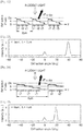
- FIG. 6 is a graph of reflectance with respect to a carrier concentration formed in the active area 135 of the permittivity variation layer 130 employed in the optical modulation device 100 of FIG. 1 .
- FIG. 7 is a graph of a phase shift with respect to a carrier concentration formed in the active area 135 of the permittivity variation layer 130 employed in the optical modulation device 100 of FIG. 1 .
- the optical modulation device 100 is capable of a 4-level phase shift with respect to light of a wavelength of 1265 nm. That is, when light of a wavelength of 1264 nm is incident onto the optical modulation device 100, a phase shift of 0, 90°, 180°, and 270° may occur by changing the carrier concentration, i.e. changing voltage applied between the metal layer 110 and the nano-antennas NA.
- Values of voltages applied between the metal layer 110 and the plurality of nano-antennas NA may have a predetermined regularity, and thus the optical modulation device 100 may function as a phase grating.
- the optical modulation device 100 may be utilized as a dynamic phase grating according to an exemplary embodiment described below with reference to FIGS. 8 through 15 below.
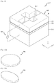
- FIG. 8 is a perspective view of a sample structure for a computer simulation in which the optical modulation device 100 is utilized as dynamic phase grating, according to an exemplary embodiment.
- FIG. 9 is a perspective view of detailed dimensions of a unit block of the sample structure of FIG. 8 .
- the sample structure used for the computer simulation may include 64 unit blocks arranged in a y direction. Dimensions of the unit blocks may be the same as shown in FIG. 9 and have a unit of nm. A boundary condition defining that the unit blocks are repeatedly continuous in an x direction may be applied during the computer simulation.
- L is equal to 180 nm, that is, a length capable of modulating light of a wavelength of 1250 nm. The operating wavelength of the device may be changed by adjusting L.
- the metal layer 110 and the nano-antennas NA are made of Au
- the permittivity variation layer 130 is made of ITO
- the permittivity dielectric material layer 150 is made of Al 2 O 3 .
- FIG. 10 is a graph of an example of a pattern of a voltage applied to the sample structure of FIG. 8 and a phase shift of incident light with respect to the voltage pattern and a direction of 1 st order diffraction light.
- the voltage V1 shown in FIG. 10 is applied between the metal layer 110 and the nano-antennas NA at a regular period ⁇ of 2 ⁇ m in the sample structure of FIG. 8 . That is, the voltage V1 may be applied between the metal layer 110 and each of the nano-antennas NA in four unit blocks in a y direction, and no voltage may be applied between the metal layer 110 and each of the nano-antennas NA in next four unit blocks. Voltages may be applied to 64 unit blocks with this regular period. The voltage V1 may be determined so that the phase shift is ⁇ , i.e., 180°.
- FIG. 11 is a graph of light intensity with respect to a diffraction angle when a voltage pattern as shown in FIG. 10 is applied to the sample structure of FIG. 8 .
- an intensity peak appears at the diffraction angles 40° and -40°, due to the symmetry of the phase grating. That is, as is shown in the graph of FIG. 10 , 1 st order diffraction light and -1 st order diffraction light may to a direction of incident light.
- FIG. 12 is a graph of another example of shapes of voltages applied to the sample structure of FIG. 8 and a resultant phase shift of incident light with respect to the voltage shapes and a direction of 1 st order diffraction light.
- the voltages V1, V2, and V3 may be applied at a regular period so that a phase grating having no symmetry may be formed.
- the voltage pattern of V1, V2, V3 of three values that may cause phase shifts of 270°, 180°, and 90°and no voltage application may be applied between the metal layer 110 and the nano-antennas NA at the period A of 2 ⁇ m. That is, the voltage V1 may be applied between each of the nano-antennas NA and the metal layer 110 in two unit blocks in a y direction, the voltage V2 may be applied between each of the nano-antennas NA and the metal layer 110 in next two unit blocks, the voltage V3 may be applied between each of the nano-antennas NA and the metal layer 110 in next two unit blocks, and no voltage may be applied between each of the nano-antennas NA and the metal layer 110 in next two unit blocks. Such a regular period may be repeatedly applied to 64 unit blocks.
- an area having the phase shift of 270°, an area having the phase shift of 180°, an area having the phase shift of 90°, and an area having no phase shift are repeated at the same period as the voltage applying period ⁇ of 2 ⁇ m along the surface of the optical modulation device 100. If light is incident onto such phase grating, as shown, it is determined that 1 st order diffraction light corresponding to a shape in which a phase gradually shifts from 270° to 0° at the period of 2 ⁇ m may .
- FIG. 13 is a graph of light intensity with respect to a diffraction angle when a voltage pattern as shown in FIG. 12 is applied to the sample structure of FIG. 8 .
- FIG. 14 is a graph of another example of shapes of the voltage applied to the sample structure of FIG. 8 and a phase shift of incident light with respect to the voltage shapes and a direction of 1 st order diffraction light.
- the voltage applying pattern of FIG. 14 has a shape in which the period ⁇ increase to 4 ⁇ m, as compared to that of FIG. 12 .
- the voltage pattern of V1, V2, V3 of three values that may cause phase shifts of 270°, 180°, 90° and no voltage application may be applied between the metal layer 110 and the nano-antennas NA at the period ⁇ of 4 ⁇ m.
- the voltage V1 may be applied between each of the nano-antennas NA and the metal layer 110 in four unit blocks in a y direction
- the voltage V2 may be applied between each of the nano-antennas NA and the metal layer 110 in next four unit blocks
- the voltage V3 may be applied between each of the nano-antennas NA and the metal layer 110 in next four unit blocks
- no voltage may be applied between each of the nano-antennas NA and the metal layer 110 in next four unit blocks.
- Such a regular period may be repeatedly applied to 64 unit blocks.
- an area having the phase shift of 270°, an area having the phase shift of 180°, an area having the phase shift of 90°, and an area having no phase shift are repeated at the same period as the voltage applying period A of 4 ⁇ m along the surface of the optical modulation device 100. If light is incident to such a phase grating, as shown, it is determined that a 1 st order diffraction light corresponding to a shape in which a phase gradually shifts from 270° to 0°at the period of 4 ⁇ m may occur.
- FIG. 15 is a graph of light intensity with respect to a diffraction angle when the voltage pattern shown in FIG. 14 is applied to the sample structure of FIG. 8 .
- the optical modulation device 100 may be used as a phase grating according to the shapes of several applied voltage. According to results above, it may be seen that a phase shift control of 2 ⁇ may be possible with respect to light of a near IR wavelength by using ITO to form the permittivity variation layer 130. Thus, light of a different wavelength band may be controlled by utilizing a different material for of permittivity variation layer 130 and/or using nano-antennas NA with shapes having different dimensions.
- the applied voltage patterns shown herein are examples.
- a regular period of the voltage pattern applied may be varied, thereby achieving various light modulation results.
- a phase shift may have various levels including 2 or 4. This may be used to perform light modulation functions such as beam shaping or beam steering.
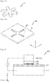
- FIG. 16 is a perspective view of a unit block of an optical modulation device 100', according to another exemplary embodiment.
- the optical modulation device 100' may include the metal layer 110, the permittivity variation layer 130, and a nano-antenna NA'.
- the nano-antenna NA' may have a shape including a nano pattern engraved in a metal material M, unlike the embossed shape of the nano-anntena NA of FIG. 2 . That is, the nano-antenna NA' may have a shape that is the inverse of the shape of the nano-anntena NA of FIG. 2 .
- a substantially cross-shaped through hole NH may be engraved in the metal material M.
- the cross-sectional shapes of the nano-antennas NA and NA' are illustrated as being substantially cross-shaped, this is merely exemplary.
- the nano-antennas NA and NA' may have any of various shapes.
- FIGS. 17A through 17D show exemplary shapes of nano-antennas that may be used in a unit block of an optical modulation device, according to exemplary embodiments.
- a cross-sectional shape of the nano-antenna NA may be circular.
- a nano-antenna NA with such a shape may be used in the optical modulation device 100 of FIG. 1 .
- a plurality of circular nano-antennas NA may be arranged to be connected to each other in one direction to form a nano-antenna line NAL.
- a cross-sectional shape of the nano-antenna NA may be oval.
- a nano-antenna NA with such a shape may be used in the optical modulation device 100 of FIG. 1 .
- a plurality of oval nano-antennas NA may be arranged to be connected to each other in one direction, for example, along a major axis, to form a nano-antenna line NAL.
- the plurality of oval nano-antennas NA may be arranged to be connected to each other in a different direction from the major axis, for example, along a minor axis or in another direction, to form the nano-antenna line NAL.
- the nano-antenna NA may have a star (*) shape in which three nano rods intersect.
- a plurality of star shape nano-antennas NA may be connected to each other in one direction, for example, a length direction of one of the three nano rods, to form the nano-antenna line NAL of the optical modulation device 100 of FIG. 1 .
- the nano-antenna NA of FIG. 17D may have a shape in which a plurality of nano pattern through holes NH are formed in the metal material M.
- a plurality of such shape of nano-antennas NA may be connected to each other, for example, in an x direction, to form the nano-antenna line NAL of FIG. 1 .
- FIGS. 17A through 17D are exemplary.
- the nano-antenna NA may have any of various shapes, for example, polygonal shapes, nano rods, etc..
- FIG. 18 is a cross-sectional view of a unit block of an optical modulation device 200, according to another exemplary embodiment.
- the optical modulation device 200 may include a metal layer 210, a dielectric material layer 250, a permittivity variation layer 230, and a nano-antenna NA.
- the optical modulation device 200 of the present embodiment is different from the optical modulation device 100 of FIG. 2 in the arrangement of the dielectric material layer 250 and the permittivity variation layer 230. That is, the dielectric material layer 250 may be provided on the metal layer 210, the permittivity variation layer 230 may be provided on the dielectric material layer 250, and the nano-antennal NA may be provided on the permittivity variation layer 230.
- the plurality of nano-antennas NA may be arranged to be connected to each other in an x direction to form the nano-antenna line NAL.
- the permittivity variation layer 230 may be patterned in the same shape as the nano-antenna NA.
- an active area 235 may be formed in the permittivity variation layer 230.
- the active area 235 may be formed in the region of the permittivity variation layer 230 adjacent to the dielectric material layer 250, may have a carrier concentration that varies according to a change in the applied voltage, and may thereby function as a gate that adjusts and controls optical modulation performance.
- FIG. 19 is a cross-sectional view of a unit block of an optical modulation device 300, according to another exemplary embodiment.
- the optical modulation device 300 may include a metal layer 310, a dielectric material layer 350, a permittivity variation layer 330, and a nano-antenna NA.
- the optical modulation device 300 of the present exemplary embodiment is different from the optical modulation device 200 of FIG. 18 in that the permittivity variation layer 330 is not patterned in the same shape as the nano-antenna NA. That is, the dielectric material layer 350 and the permittivity variation layer 330 may be formed on an entire surface the metal layer 310, and the nano-antenna NA may be formed in a predetermined pattern on the permittivity variation layer 330.
- the plurality of nano-antennas NA may be arranged to be connected to each other in an x direction to form the nano-antenna line NAL.
- an active area 335 may be formed in the permittivity variation layer 330.
- the active area 335 may be formed in a region of the permittivity variation layer 330 adjacent to the dielectric material layer 350, may have a carrier concentration that varies according to a change in the applied voltage, and may thereby function as a gate that adjusts and controls optical modulation performance.
- a material of a permittivity variation layer, a shape and/or dimensions of a nano-antenna, and a form of the applied voltage may be changed in any of various ways, thereby providing various optical modulation performances in a desired wavelength band.
- a plurality of nano-antennas may be arranged in a matrix shape to form a plasmonic nano-antenna layer, and voltage applying means may be configured to individually control the voltage between each of the nano-antennas and a metal layer.
- the nano-antennas included in the plasmonic nano-antenna layers illustrated herein have the same shape, but this is merely exemplary.
- Nano-antennas within the same plasmonic nano-antenna layer may have different shapes.
- nano-antennas in the same plasmonic nano--antenna layer may have the same shape, but different dimensions, so that a resonance wavelength band may be differently in each area.
- the above-described optical modulation device may include the plasmonic nano-antenna layer and the permittivity variation layer and may modulate incident light in any of various shapes by utilizing, as a gate, an area of the permittivity variation layer in which a carrier concentration varies.
- the above-described optical modulation device may be manufactured to have a small size and may enable fast driving.
- the optical modulation device may be used in any of various optical apparatuses, thereby improving the performance thereof.
Landscapes
- Physics & Mathematics (AREA)
- Nonlinear Science (AREA)
- Optics & Photonics (AREA)
- General Physics & Mathematics (AREA)
- Chemical & Material Sciences (AREA)
- Engineering & Computer Science (AREA)
- Nanotechnology (AREA)
- Life Sciences & Earth Sciences (AREA)
- Biophysics (AREA)
- Crystallography & Structural Chemistry (AREA)
- Optical Modulation, Optical Deflection, Nonlinear Optics, Optical Demodulation, Optical Logic Elements (AREA)
Claims (15)
- Optische Modulationsvorrichtung (100), umfassend:eine plasmonische Nanoantennenschicht (170);eine Metallschicht (110);eine Permittivitätsvariationsschicht (130), umfassend ein elektrooptisches Material, das zwischen der plasmonischen Nanoantennenschicht und der Metallschicht angeordnet ist, wobei die Permittivitätsvariationsschicht eine Permittivität aufweist, die gemäß einem daran angelegten elektrischen Signal variiert;eine dielektrische Materialschicht (150), die zwischen der plasmonischen Nanoantennenschicht und der Metallschicht angeordnet ist;und ein Signalanwendungsmittel (190), umfassend eine Stromquelle, die konfiguriert ist, um ein Spannungssignal zwischen der plasmonischen Nanoantennenschicht und der Metallschicht anzulegen, wobei dadurch eine Änderung der Permittivität der Permittivitätsvariationsschicht verursacht wird;dadurch gekennzeichnet, dass die plasmonische Nanoantennenschicht eine Vielzahl von Nanoantennenleitungen (NAL) umfasst, die in einer ersten Richtung (y) voneinander beabstandet sind, wobei jede der Vielzahl von Nanoantennenleitungen eine in einer zweiten Richtung (x) miteinander verbundene Vielzahl von Nanoantennen (NA) umfasst, die sich von der ersten Richtung unterscheidet;und dadurch, dass die Stromquelle so konfiguriert ist, dass sie unabhängig ein Spannungssignal zwischen jeder jeweiligen der Vielzahl von Nanoantennenleitungen und der Metallschicht anlegt.
- Optische Modulationsvorrichtung nach Anspruch 1, wobei Werte von Spannungen, die zwischen der Metallschicht (110) und jeder der Vielzahl von Nanoantennenleitungen (NAL) angelegt werden, eine vorbestimmte Regelmäßigkeit in der ersten Richtung (y) aufweisen.
- Optische Modulationsvorrichtung nach Anspruch 1 oder 2, wobei die Permittivitätsvariationsschicht (130) umfasst: ein transparentes leitfähiges Material; und/oder ein Übergangsmetallnitrid.
- Optische Modulationsvorrichtung nach einem der vorhergehenden Ansprüche, wobei die Permittivitätsvariationsschicht (130) einen aktiven Bereich (135) mit einer Trägerkonzentration umfasst, die gemäß einer zwischen der plasmonischen Nanoantennenschicht (170) und der Metallschicht (110) angelegten Spannung variiert.
- Optische Modulationsvorrichtung nach Anspruch 4, wobei der aktive Bereich (135) der Permittivitätsvariationsschicht der dielektrischen Materialschicht (150) benachbart ist.
- Optische Modulationsvorrichtung nach Anspruch 4 oder 5, wobei der Realteil der Dielektrizitätskonstante der Permittivitätsvariationsschicht (130) in einem vorbestimmten Wellenlängenband gleich 0 ist.
- Optische Modulationsvorrichtung nach Anspruch 6, wobei das vorbestimmte Wellenlängenband gemäß der Trägerkonzentration in dem aktiven Bereich (135) unterschiedlich ist.
- Optische Modulationsvorrichtung nach Anspruch 6 oder 7, wobei die von der Stromquelle zwischen der plasmonischen Nanoantennenschicht (170) und der Metallschicht (110) angelegte Spannung in einem Bereich liegt, der einen Spannungswert enthält, bei dem ein Resonanzwellenlängenband der plasmonischen Nanoantennenschicht und das vorbestimmte Wellenlängenband identisch sind.
- Optische Modulationsvorrichtung nach einem der vorhergehenden Ansprüche, wobei jede der Vielzahl von Nanoantennen (NA) eine Kreuzform aufweist, bei der sich ein Nanostab mit einer Länge in der ersten Richtung (y) und ein Nanostab mit einer Länge in der zweiten Richtung (x) kreuzen.
- Optische Modulationsvorrichtung nach einem der Ansprüche 1 bis 8, wobei jede der Vielzahl von Nanoantennen (NA) kreisförmig, oval, polygonal, X-förmig oder sternförmig ist.
- Optische Modulationsvorrichtung nach einem der vorhergehenden Ansprüche, wobei die Permittivitätsvariationsschicht (130) auf der Metallschicht (110) und die dielektrische Materialschicht (150) auf der Permittivitätsvariationsschicht angeordnet ist.
- Optische Modulationsvorrichtung nach einem der Ansprüche 1 bis 10, wobei die dielektrische Materialschicht (150) auf der Metallschicht (110) und die Permittivitätsvariationsschicht (130) auf der dielektrischen Materialschicht angeordnet ist.
- Optische Modulationsvorrichtung nach Anspruch 12, wobei die Permittivitätsvariationsschicht (150) in der gleichen Form wie die plasmonische Nanoantennenschicht (170) strukturiert ist.
- Optische Modulationsvorrichtung nach einem der vorhergehenden Ansprüche, wobei die plasmonische Nanoantennenschicht (170) ein Metallmaterial und ein Nanomuster aus einer Vielzahl von Durchgangslöchern umfasst, die in dem Metallmaterial ausgebildet sind.
- Optische Vorrichtung, umfassend die optische Modulationsvorrichtung nach Anspruch 1.
Applications Claiming Priority (4)
| Application Number | Priority Date | Filing Date | Title |
|---|---|---|---|
| US201562111583P | 2015-02-03 | 2015-02-03 | |
| KR1020150107515A KR102374119B1 (ko) | 2015-02-03 | 2015-07-29 | 게이트 구조를 포함하는 광 변조 소자 |
| US15/010,967 US9632216B2 (en) | 2015-02-03 | 2016-01-29 | Optical modulating device having gate structure |
| PCT/US2016/016475 WO2016126896A1 (en) | 2015-02-03 | 2016-02-03 | Optical modulating device having gate structure |
Publications (3)
| Publication Number | Publication Date |
|---|---|
| EP3254154A1 EP3254154A1 (de) | 2017-12-13 |
| EP3254154A4 EP3254154A4 (de) | 2018-09-19 |
| EP3254154B1 true EP3254154B1 (de) | 2020-05-06 |
Family
ID=56854503
Family Applications (1)
| Application Number | Title | Priority Date | Filing Date |
|---|---|---|---|
| EP16747249.7A Active EP3254154B1 (de) | 2015-02-03 | 2016-02-03 | Optische modulationsvorrichtung mit gate-struktur |
Country Status (4)
| Country | Link |
|---|---|
| EP (1) | EP3254154B1 (de) |
| JP (1) | JP6849597B2 (de) |
| KR (1) | KR102374119B1 (de) |
| CN (1) | CN107209436B (de) |
Cited By (1)
| Publication number | Priority date | Publication date | Assignee | Title |
|---|---|---|---|---|
| US11480918B2 (en) | 2019-02-28 | 2022-10-25 | Samsung Electronics Co., Ltd. | Active complex spatial light modulation method and apparatus for an ultra-low noise holographic display |
Families Citing this family (30)
| Publication number | Priority date | Publication date | Assignee | Title |
|---|---|---|---|---|
| KR102529893B1 (ko) * | 2015-08-10 | 2023-05-08 | 삼성전자주식회사 | 메타 구조체 및 이를 포함하는 가변 광학 소자 |
| US10191308B2 (en) | 2015-12-10 | 2019-01-29 | Samsung Electronics Co., Ltd. | Optoelectronic device and smart window comprising the same |
| KR102698289B1 (ko) * | 2016-08-23 | 2024-08-23 | 삼성전자주식회사 | 광 변조기, 빔 스티어링 소자 및 이를 적용한 시스템 |
| KR102698288B1 (ko) * | 2016-08-24 | 2024-08-23 | 삼성전자주식회사 | 위상 변조 능동 소자, 이의 구동 방법 및 위상 변조 능동 소자를 포함하는 광학 장치 |
| KR102530559B1 (ko) * | 2016-08-29 | 2023-05-09 | 삼성전자주식회사 | 레이저빔 스티어링 소자 및 이를 포함하는 시스템 |
| KR102698290B1 (ko) * | 2016-09-09 | 2024-08-23 | 삼성전자주식회사 | 위상 변조 능동 소자, 이의 구동 방법 및 위상 변조 능동 소자를 포함하는 광학 장치 |
| KR102754868B1 (ko) * | 2016-11-16 | 2025-01-14 | 삼성전자주식회사 | 2차원 광 변조 소자 및 이를 포함하는 전자 기기 |
| WO2018209250A1 (en) * | 2017-05-11 | 2018-11-15 | Baylor University | Field-effect tunable epsilon-near-zero absorber |
| EP4488746A3 (de) * | 2017-06-30 | 2025-03-26 | The Board of Trustees of the Leland Stanford Junior University | Akustooptisches strahllenksystem |
| KR102372090B1 (ko) * | 2017-07-13 | 2022-03-08 | 삼성전자주식회사 | 광변조 소자와 그 동작방법 및 광변조 소자를 포함하는 장치 |
| KR102411663B1 (ko) * | 2017-09-05 | 2022-06-21 | 삼성전자주식회사 | 광 변조 소자 및 이를 포함하는 전자 기기 |
| KR102506440B1 (ko) * | 2017-09-13 | 2023-03-06 | 삼성전자주식회사 | 빔 스캐닝 장치 및 이를 포함하는 광학 장치 |
| KR102613049B1 (ko) * | 2017-10-10 | 2023-12-12 | 삼성전자주식회사 | 양자점 광변조기 및 이를 포함하는 장치 |
| KR102542468B1 (ko) * | 2017-10-31 | 2023-06-14 | 삼성전자주식회사 | 출력 커플러를 포함하는 광방출 소자 및 이를 적용한 광학 장치 |
| EP3477364B1 (de) | 2017-10-31 | 2023-11-22 | Samsung Electronics Co., Ltd. | Lichtemissionsvorrichtung mit ausgangskoppler und optisches vorrichtung damit |
| CN108181736A (zh) * | 2018-01-08 | 2018-06-19 | 苏州大学 | 基于石墨烯/金属复合结构的电光调制器 |
| CN108563040A (zh) * | 2018-01-08 | 2018-09-21 | 苏州大学 | 基于石墨烯/金属混合结构的光开关 |
| US11085996B2 (en) * | 2018-03-23 | 2021-08-10 | Samsung Electronics Co., Ltd. | Beam scanning apparatus and optical apparatus including the same |
| KR102592695B1 (ko) * | 2018-03-23 | 2023-10-23 | 삼성전자주식회사 | 빔 스캐닝 장치 및 이를 포함하는 광학 장치 |
| US10968522B2 (en) * | 2018-04-02 | 2021-04-06 | Elwha Llc | Fabrication of metallic optical metasurfaces |
| KR102568796B1 (ko) * | 2018-06-15 | 2023-08-21 | 삼성전자주식회사 | 광변조 소자 및 이를 포함하는 장치 |
| WO2019246012A1 (en) * | 2018-06-19 | 2019-12-26 | Baylor University | Metasurface on optical fiber and related method |
| US10777970B2 (en) * | 2018-09-04 | 2020-09-15 | Samsung Electronics Co., Ltd. | Metamaterial-based reflector, optical cavity structure including the same and vertical cavity surface emitting laser |
| KR102682127B1 (ko) * | 2018-11-07 | 2024-07-08 | 삼성전자주식회사 | 광변조 소자와 그 동작방법 및 광변조 소자를 포함하는 장치 |
| CN109935972B (zh) * | 2019-01-25 | 2021-01-26 | 南通大学 | 一种基于等离子体激元的宽带天线 |
| KR102506448B1 (ko) * | 2019-02-28 | 2023-03-06 | 삼성전자주식회사 | 초저잡음 홀로그래픽 디스플레이를 위한 능동 복소 공간 광 변조 방법 및 장치 |
| JP6766277B1 (ja) * | 2019-06-20 | 2020-10-07 | 三菱電機株式会社 | 反射光学素子 |
| US11843171B2 (en) | 2020-08-18 | 2023-12-12 | Samsung Electronics Co., Ltd. | Multi-layer reconfigurable surface for an antenna |
| CN114578586A (zh) * | 2022-03-03 | 2022-06-03 | 上海匕令科技有限公司 | 光束控制装置 |
| CN116577863B (zh) * | 2023-05-16 | 2025-09-09 | 扬州大学 | 一种超表面四分之一波片 |
Family Cites Families (8)
| Publication number | Priority date | Publication date | Assignee | Title |
|---|---|---|---|---|
| US6040936A (en) * | 1998-10-08 | 2000-03-21 | Nec Research Institute, Inc. | Optical transmission control apparatus utilizing metal films perforated with subwavelength-diameter holes |
| WO2010004859A1 (ja) * | 2008-07-08 | 2010-01-14 | 学校法人慶應義塾 | プラズモン導波路及びそれを用いた光素子 |
| US8134774B2 (en) * | 2009-04-16 | 2012-03-13 | Shih-Yuan Wang | Dynamically reconfigurable negative index material crossbars with gain |
| KR101669219B1 (ko) * | 2010-12-30 | 2016-10-26 | 삼성전자주식회사 | 광변조기 및 이를 채용한 광학장치 |
| WO2012123620A1 (en) * | 2011-03-16 | 2012-09-20 | Aalto University Foundation | Thin film photovoltaic cell structure, nanoantenna, and method for manufacturing |
| US20140085693A1 (en) * | 2012-09-26 | 2014-03-27 | Northeastern University | Metasurface nanoantennas for light processing |
| US9244268B2 (en) * | 2013-02-14 | 2016-01-26 | The United States Of America, As Represented By The Secretary Of The Navy | Actively tunable polar-dielectric optical devices |
| US9958707B2 (en) * | 2014-03-06 | 2018-05-01 | California Institute Of Technology | Systems and methods for implementing electrically tunable metasurfaces |
-
2015
- 2015-07-29 KR KR1020150107515A patent/KR102374119B1/ko active Active
-
2016
- 2016-02-03 EP EP16747249.7A patent/EP3254154B1/de active Active
- 2016-02-03 JP JP2017536574A patent/JP6849597B2/ja active Active
- 2016-02-03 CN CN201680008540.1A patent/CN107209436B/zh active Active
Non-Patent Citations (1)
| Title |
|---|
| None * |
Cited By (1)
| Publication number | Priority date | Publication date | Assignee | Title |
|---|---|---|---|---|
| US11480918B2 (en) | 2019-02-28 | 2022-10-25 | Samsung Electronics Co., Ltd. | Active complex spatial light modulation method and apparatus for an ultra-low noise holographic display |
Also Published As
| Publication number | Publication date |
|---|---|
| KR20160096527A (ko) | 2016-08-16 |
| CN107209436B (zh) | 2020-09-11 |
| JP2018509643A (ja) | 2018-04-05 |
| JP6849597B2 (ja) | 2021-03-24 |
| KR102374119B1 (ko) | 2022-03-14 |
| EP3254154A4 (de) | 2018-09-19 |
| CN107209436A (zh) | 2017-09-26 |
| EP3254154A1 (de) | 2017-12-13 |
Similar Documents
| Publication | Publication Date | Title |
|---|---|---|
| EP3254154B1 (de) | Optische modulationsvorrichtung mit gate-struktur | |
| US9632216B2 (en) | Optical modulating device having gate structure | |
| EP3182200B1 (de) | Lichtmodulationsvorrichtung einschliesslich einer dielektrischen antenne | |
| JP7164331B2 (ja) | 光変調素子 | |
| KR101669219B1 (ko) | 광변조기 및 이를 채용한 광학장치 | |
| US10802301B2 (en) | Active metasurfaces for dynamic polarization conversion | |
| Vasić et al. | Tunable beam steering at terahertz frequencies using reconfigurable metasurfaces coupled with liquid crystals | |
| KR20180022100A (ko) | 광 변조기, 빔 스티어링 소자 및 이를 적용한 시스템 | |
| US10302995B2 (en) | High reflectivity LCOS device | |
| KR101905444B1 (ko) | 능동형 메타표면, 이를 포함한 광학소자 및 이의 제조방법 | |
| US11468912B2 (en) | Device and arrangement for controlling an electromagnetic wave, methods of forming and operating the same | |
| US10989936B2 (en) | Optical modulation device including mirror elements and nano-antenna array, method of operating the same, and apparatus including the optical modulation device | |
| CN117769663A (zh) | 用于大角度波束控制和lidar应用的电控超表面 | |
| CN106707559B (zh) | 基于石墨烯二维超材料的功能器件 | |
| US12174513B2 (en) | Optical modulating device and optical apparatus employing the same | |
| KR20170068372A (ko) | 메타 소자 | |
| CN114761883B (zh) | 包含平面的超表面的电控动态光学组件 | |
| CN116745665B (zh) | 包括超表面的电控动态光学组件 | |
| CN114005932B (zh) | 一种基于相变材料的可控超表面结构及其制备方法 | |
| WO2022085455A1 (ja) | 光変調器及び光変調器アレイ |
Legal Events
| Date | Code | Title | Description |
|---|---|---|---|
| STAA | Information on the status of an ep patent application or granted ep patent |
Free format text: STATUS: THE INTERNATIONAL PUBLICATION HAS BEEN MADE |
|
| PUAI | Public reference made under article 153(3) epc to a published international application that has entered the european phase |
Free format text: ORIGINAL CODE: 0009012 |
|
| STAA | Information on the status of an ep patent application or granted ep patent |
Free format text: STATUS: REQUEST FOR EXAMINATION WAS MADE |
|
| 17P | Request for examination filed |
Effective date: 20170904 |
|
| AK | Designated contracting states |
Kind code of ref document: A1 Designated state(s): AL AT BE BG CH CY CZ DE DK EE ES FI FR GB GR HR HU IE IS IT LI LT LU LV MC MK MT NL NO PL PT RO RS SE SI SK SM TR |
|
| AX | Request for extension of the european patent |
Extension state: BA ME |
|
| DAV | Request for validation of the european patent (deleted) | ||
| DAX | Request for extension of the european patent (deleted) | ||
| A4 | Supplementary search report drawn up and despatched |
Effective date: 20180821 |
|
| RIC1 | Information provided on ipc code assigned before grant |
Ipc: G02F 1/19 20060101ALI20180814BHEP Ipc: G02F 1/01 20060101AFI20180814BHEP Ipc: B82Y 20/00 20110101ALI20180814BHEP Ipc: G02B 5/00 20060101ALI20180814BHEP |
|
| GRAP | Despatch of communication of intention to grant a patent |
Free format text: ORIGINAL CODE: EPIDOSNIGR1 |
|
| STAA | Information on the status of an ep patent application or granted ep patent |
Free format text: STATUS: GRANT OF PATENT IS INTENDED |
|
| INTG | Intention to grant announced |
Effective date: 20191216 |
|
| GRAS | Grant fee paid |
Free format text: ORIGINAL CODE: EPIDOSNIGR3 |
|
| GRAA | (expected) grant |
Free format text: ORIGINAL CODE: 0009210 |
|
| STAA | Information on the status of an ep patent application or granted ep patent |
Free format text: STATUS: THE PATENT HAS BEEN GRANTED |
|
| AK | Designated contracting states |
Kind code of ref document: B1 Designated state(s): AL AT BE BG CH CY CZ DE DK EE ES FI FR GB GR HR HU IE IS IT LI LT LU LV MC MK MT NL NO PL PT RO RS SE SI SK SM TR |
|
| REG | Reference to a national code |
Ref country code: GB Ref legal event code: FG4D |
|
| REG | Reference to a national code |
Ref country code: AT Ref legal event code: REF Ref document number: 1267710 Country of ref document: AT Kind code of ref document: T Effective date: 20200515 Ref country code: CH Ref legal event code: EP |
|
| REG | Reference to a national code |
Ref country code: IE Ref legal event code: FG4D |
|
| REG | Reference to a national code |
Ref country code: DE Ref legal event code: R096 Ref document number: 602016035822 Country of ref document: DE |
|
| REG | Reference to a national code |
Ref country code: LT Ref legal event code: MG4D |
|
| REG | Reference to a national code |
Ref country code: NL Ref legal event code: MP Effective date: 20200506 |
|
| PG25 | Lapsed in a contracting state [announced via postgrant information from national office to epo] |
Ref country code: PT Free format text: LAPSE BECAUSE OF FAILURE TO SUBMIT A TRANSLATION OF THE DESCRIPTION OR TO PAY THE FEE WITHIN THE PRESCRIBED TIME-LIMIT Effective date: 20200907 Ref country code: LT Free format text: LAPSE BECAUSE OF FAILURE TO SUBMIT A TRANSLATION OF THE DESCRIPTION OR TO PAY THE FEE WITHIN THE PRESCRIBED TIME-LIMIT Effective date: 20200506 Ref country code: GR Free format text: LAPSE BECAUSE OF FAILURE TO SUBMIT A TRANSLATION OF THE DESCRIPTION OR TO PAY THE FEE WITHIN THE PRESCRIBED TIME-LIMIT Effective date: 20200807 Ref country code: FI Free format text: LAPSE BECAUSE OF FAILURE TO SUBMIT A TRANSLATION OF THE DESCRIPTION OR TO PAY THE FEE WITHIN THE PRESCRIBED TIME-LIMIT Effective date: 20200506 Ref country code: IS Free format text: LAPSE BECAUSE OF FAILURE TO SUBMIT A TRANSLATION OF THE DESCRIPTION OR TO PAY THE FEE WITHIN THE PRESCRIBED TIME-LIMIT Effective date: 20200906 Ref country code: NO Free format text: LAPSE BECAUSE OF FAILURE TO SUBMIT A TRANSLATION OF THE DESCRIPTION OR TO PAY THE FEE WITHIN THE PRESCRIBED TIME-LIMIT Effective date: 20200806 Ref country code: SE Free format text: LAPSE BECAUSE OF FAILURE TO SUBMIT A TRANSLATION OF THE DESCRIPTION OR TO PAY THE FEE WITHIN THE PRESCRIBED TIME-LIMIT Effective date: 20200506 |
|
| PG25 | Lapsed in a contracting state [announced via postgrant information from national office to epo] |
Ref country code: BG Free format text: LAPSE BECAUSE OF FAILURE TO SUBMIT A TRANSLATION OF THE DESCRIPTION OR TO PAY THE FEE WITHIN THE PRESCRIBED TIME-LIMIT Effective date: 20200806 Ref country code: RS Free format text: LAPSE BECAUSE OF FAILURE TO SUBMIT A TRANSLATION OF THE DESCRIPTION OR TO PAY THE FEE WITHIN THE PRESCRIBED TIME-LIMIT Effective date: 20200506 Ref country code: HR Free format text: LAPSE BECAUSE OF FAILURE TO SUBMIT A TRANSLATION OF THE DESCRIPTION OR TO PAY THE FEE WITHIN THE PRESCRIBED TIME-LIMIT Effective date: 20200506 Ref country code: LV Free format text: LAPSE BECAUSE OF FAILURE TO SUBMIT A TRANSLATION OF THE DESCRIPTION OR TO PAY THE FEE WITHIN THE PRESCRIBED TIME-LIMIT Effective date: 20200506 |
|
| REG | Reference to a national code |
Ref country code: AT Ref legal event code: MK05 Ref document number: 1267710 Country of ref document: AT Kind code of ref document: T Effective date: 20200506 |
|
| PG25 | Lapsed in a contracting state [announced via postgrant information from national office to epo] |
Ref country code: AL Free format text: LAPSE BECAUSE OF FAILURE TO SUBMIT A TRANSLATION OF THE DESCRIPTION OR TO PAY THE FEE WITHIN THE PRESCRIBED TIME-LIMIT Effective date: 20200506 Ref country code: NL Free format text: LAPSE BECAUSE OF FAILURE TO SUBMIT A TRANSLATION OF THE DESCRIPTION OR TO PAY THE FEE WITHIN THE PRESCRIBED TIME-LIMIT Effective date: 20200506 |
|
| PG25 | Lapsed in a contracting state [announced via postgrant information from national office to epo] |
Ref country code: RO Free format text: LAPSE BECAUSE OF FAILURE TO SUBMIT A TRANSLATION OF THE DESCRIPTION OR TO PAY THE FEE WITHIN THE PRESCRIBED TIME-LIMIT Effective date: 20200506 Ref country code: AT Free format text: LAPSE BECAUSE OF FAILURE TO SUBMIT A TRANSLATION OF THE DESCRIPTION OR TO PAY THE FEE WITHIN THE PRESCRIBED TIME-LIMIT Effective date: 20200506 Ref country code: CZ Free format text: LAPSE BECAUSE OF FAILURE TO SUBMIT A TRANSLATION OF THE DESCRIPTION OR TO PAY THE FEE WITHIN THE PRESCRIBED TIME-LIMIT Effective date: 20200506 Ref country code: ES Free format text: LAPSE BECAUSE OF FAILURE TO SUBMIT A TRANSLATION OF THE DESCRIPTION OR TO PAY THE FEE WITHIN THE PRESCRIBED TIME-LIMIT Effective date: 20200506 Ref country code: DK Free format text: LAPSE BECAUSE OF FAILURE TO SUBMIT A TRANSLATION OF THE DESCRIPTION OR TO PAY THE FEE WITHIN THE PRESCRIBED TIME-LIMIT Effective date: 20200506 Ref country code: SM Free format text: LAPSE BECAUSE OF FAILURE TO SUBMIT A TRANSLATION OF THE DESCRIPTION OR TO PAY THE FEE WITHIN THE PRESCRIBED TIME-LIMIT Effective date: 20200506 Ref country code: IT Free format text: LAPSE BECAUSE OF FAILURE TO SUBMIT A TRANSLATION OF THE DESCRIPTION OR TO PAY THE FEE WITHIN THE PRESCRIBED TIME-LIMIT Effective date: 20200506 Ref country code: EE Free format text: LAPSE BECAUSE OF FAILURE TO SUBMIT A TRANSLATION OF THE DESCRIPTION OR TO PAY THE FEE WITHIN THE PRESCRIBED TIME-LIMIT Effective date: 20200506 |
|
| REG | Reference to a national code |
Ref country code: DE Ref legal event code: R097 Ref document number: 602016035822 Country of ref document: DE |
|
| PG25 | Lapsed in a contracting state [announced via postgrant information from national office to epo] |
Ref country code: SK Free format text: LAPSE BECAUSE OF FAILURE TO SUBMIT A TRANSLATION OF THE DESCRIPTION OR TO PAY THE FEE WITHIN THE PRESCRIBED TIME-LIMIT Effective date: 20200506 Ref country code: PL Free format text: LAPSE BECAUSE OF FAILURE TO SUBMIT A TRANSLATION OF THE DESCRIPTION OR TO PAY THE FEE WITHIN THE PRESCRIBED TIME-LIMIT Effective date: 20200506 |
|
| PLBE | No opposition filed within time limit |
Free format text: ORIGINAL CODE: 0009261 |
|
| STAA | Information on the status of an ep patent application or granted ep patent |
Free format text: STATUS: NO OPPOSITION FILED WITHIN TIME LIMIT |
|
| 26N | No opposition filed |
Effective date: 20210209 |
|
| PG25 | Lapsed in a contracting state [announced via postgrant information from national office to epo] |
Ref country code: SI Free format text: LAPSE BECAUSE OF FAILURE TO SUBMIT A TRANSLATION OF THE DESCRIPTION OR TO PAY THE FEE WITHIN THE PRESCRIBED TIME-LIMIT Effective date: 20200506 |
|
| PG25 | Lapsed in a contracting state [announced via postgrant information from national office to epo] |
Ref country code: MC Free format text: LAPSE BECAUSE OF FAILURE TO SUBMIT A TRANSLATION OF THE DESCRIPTION OR TO PAY THE FEE WITHIN THE PRESCRIBED TIME-LIMIT Effective date: 20200506 |
|
| REG | Reference to a national code |
Ref country code: BE Ref legal event code: MM Effective date: 20210228 |
|
| PG25 | Lapsed in a contracting state [announced via postgrant information from national office to epo] |
Ref country code: CH Free format text: LAPSE BECAUSE OF NON-PAYMENT OF DUE FEES Effective date: 20210228 Ref country code: LI Free format text: LAPSE BECAUSE OF NON-PAYMENT OF DUE FEES Effective date: 20210228 Ref country code: LU Free format text: LAPSE BECAUSE OF NON-PAYMENT OF DUE FEES Effective date: 20210203 |
|
| PG25 | Lapsed in a contracting state [announced via postgrant information from national office to epo] |
Ref country code: IE Free format text: LAPSE BECAUSE OF NON-PAYMENT OF DUE FEES Effective date: 20210203 |
|
| PG25 | Lapsed in a contracting state [announced via postgrant information from national office to epo] |
Ref country code: BE Free format text: LAPSE BECAUSE OF NON-PAYMENT OF DUE FEES Effective date: 20210228 |
|
| PG25 | Lapsed in a contracting state [announced via postgrant information from national office to epo] |
Ref country code: CY Free format text: LAPSE BECAUSE OF FAILURE TO SUBMIT A TRANSLATION OF THE DESCRIPTION OR TO PAY THE FEE WITHIN THE PRESCRIBED TIME-LIMIT Effective date: 20200506 |
|
| PG25 | Lapsed in a contracting state [announced via postgrant information from national office to epo] |
Ref country code: HU Free format text: LAPSE BECAUSE OF FAILURE TO SUBMIT A TRANSLATION OF THE DESCRIPTION OR TO PAY THE FEE WITHIN THE PRESCRIBED TIME-LIMIT; INVALID AB INITIO Effective date: 20160203 |
|
| PG25 | Lapsed in a contracting state [announced via postgrant information from national office to epo] |
Ref country code: MK Free format text: LAPSE BECAUSE OF FAILURE TO SUBMIT A TRANSLATION OF THE DESCRIPTION OR TO PAY THE FEE WITHIN THE PRESCRIBED TIME-LIMIT Effective date: 20200506 |
|
| PG25 | Lapsed in a contracting state [announced via postgrant information from national office to epo] |
Ref country code: MT Free format text: LAPSE BECAUSE OF FAILURE TO SUBMIT A TRANSLATION OF THE DESCRIPTION OR TO PAY THE FEE WITHIN THE PRESCRIBED TIME-LIMIT Effective date: 20200506 |
|
| PGFP | Annual fee paid to national office [announced via postgrant information from national office to epo] |
Ref country code: DE Payment date: 20250121 Year of fee payment: 10 |
|
| PGFP | Annual fee paid to national office [announced via postgrant information from national office to epo] |
Ref country code: FR Payment date: 20250121 Year of fee payment: 10 |
|
| PGFP | Annual fee paid to national office [announced via postgrant information from national office to epo] |
Ref country code: GB Payment date: 20250116 Year of fee payment: 10 |
|
| PG25 | Lapsed in a contracting state [announced via postgrant information from national office to epo] |
Ref country code: TR Free format text: LAPSE BECAUSE OF FAILURE TO SUBMIT A TRANSLATION OF THE DESCRIPTION OR TO PAY THE FEE WITHIN THE PRESCRIBED TIME-LIMIT Effective date: 20200506 |