EP3249701A1 - Deep ultraviolet led and production method therefor - Google Patents
Deep ultraviolet led and production method therefor Download PDFInfo
- Publication number
- EP3249701A1 EP3249701A1 EP16861100.2A EP16861100A EP3249701A1 EP 3249701 A1 EP3249701 A1 EP 3249701A1 EP 16861100 A EP16861100 A EP 16861100A EP 3249701 A1 EP3249701 A1 EP 3249701A1
- Authority
- EP
- European Patent Office
- Prior art keywords
- layer
- photonic crystal
- algan
- periodic structure
- equal
- Prior art date
- Legal status (The legal status is an assumption and is not a legal conclusion. Google has not performed a legal analysis and makes no representation as to the accuracy of the status listed.)
- Granted
Links
Images

















Classifications
-
- H—ELECTRICITY
- H10—SEMICONDUCTOR DEVICES; ELECTRIC SOLID-STATE DEVICES NOT OTHERWISE PROVIDED FOR
- H10H—INORGANIC LIGHT-EMITTING SEMICONDUCTOR DEVICES HAVING POTENTIAL BARRIERS
- H10H20/00—Individual inorganic light-emitting semiconductor devices having potential barriers, e.g. light-emitting diodes [LED]
- H10H20/80—Constructional details
- H10H20/81—Bodies
- H10H20/817—Bodies characterised by the crystal structures or orientations, e.g. polycrystalline, amorphous or porous
-
- H—ELECTRICITY
- H10—SEMICONDUCTOR DEVICES; ELECTRIC SOLID-STATE DEVICES NOT OTHERWISE PROVIDED FOR
- H10H—INORGANIC LIGHT-EMITTING SEMICONDUCTOR DEVICES HAVING POTENTIAL BARRIERS
- H10H20/00—Individual inorganic light-emitting semiconductor devices having potential barriers, e.g. light-emitting diodes [LED]
- H10H20/80—Constructional details
- H10H20/81—Bodies
- H10H20/822—Materials of the light-emitting regions
- H10H20/824—Materials of the light-emitting regions comprising only Group III-V materials, e.g. GaP
- H10H20/825—Materials of the light-emitting regions comprising only Group III-V materials, e.g. GaP containing nitrogen, e.g. GaN
-
- H—ELECTRICITY
- H10—SEMICONDUCTOR DEVICES; ELECTRIC SOLID-STATE DEVICES NOT OTHERWISE PROVIDED FOR
- H10H—INORGANIC LIGHT-EMITTING SEMICONDUCTOR DEVICES HAVING POTENTIAL BARRIERS
- H10H20/00—Individual inorganic light-emitting semiconductor devices having potential barriers, e.g. light-emitting diodes [LED]
- H10H20/01—Manufacture or treatment
- H10H20/011—Manufacture or treatment of bodies, e.g. forming semiconductor layers
- H10H20/013—Manufacture or treatment of bodies, e.g. forming semiconductor layers having light-emitting regions comprising only Group III-V materials
- H10H20/0137—Manufacture or treatment of bodies, e.g. forming semiconductor layers having light-emitting regions comprising only Group III-V materials the light-emitting regions comprising nitride materials
-
- H—ELECTRICITY
- H10—SEMICONDUCTOR DEVICES; ELECTRIC SOLID-STATE DEVICES NOT OTHERWISE PROVIDED FOR
- H10H—INORGANIC LIGHT-EMITTING SEMICONDUCTOR DEVICES HAVING POTENTIAL BARRIERS
- H10H20/00—Individual inorganic light-emitting semiconductor devices having potential barriers, e.g. light-emitting diodes [LED]
- H10H20/80—Constructional details
- H10H20/81—Bodies
- H10H20/811—Bodies having quantum effect structures or superlattices, e.g. tunnel junctions
-
- H—ELECTRICITY
- H10—SEMICONDUCTOR DEVICES; ELECTRIC SOLID-STATE DEVICES NOT OTHERWISE PROVIDED FOR
- H10H—INORGANIC LIGHT-EMITTING SEMICONDUCTOR DEVICES HAVING POTENTIAL BARRIERS
- H10H20/00—Individual inorganic light-emitting semiconductor devices having potential barriers, e.g. light-emitting diodes [LED]
- H10H20/80—Constructional details
- H10H20/81—Bodies
- H10H20/814—Bodies having reflecting means, e.g. semiconductor Bragg reflectors
-
- H—ELECTRICITY
- H10—SEMICONDUCTOR DEVICES; ELECTRIC SOLID-STATE DEVICES NOT OTHERWISE PROVIDED FOR
- H10H—INORGANIC LIGHT-EMITTING SEMICONDUCTOR DEVICES HAVING POTENTIAL BARRIERS
- H10H20/00—Individual inorganic light-emitting semiconductor devices having potential barriers, e.g. light-emitting diodes [LED]
- H10H20/80—Constructional details
- H10H20/81—Bodies
- H10H20/815—Bodies having stress relaxation structures, e.g. buffer layers
-
- H—ELECTRICITY
- H10—SEMICONDUCTOR DEVICES; ELECTRIC SOLID-STATE DEVICES NOT OTHERWISE PROVIDED FOR
- H10H—INORGANIC LIGHT-EMITTING SEMICONDUCTOR DEVICES HAVING POTENTIAL BARRIERS
- H10H20/00—Individual inorganic light-emitting semiconductor devices having potential barriers, e.g. light-emitting diodes [LED]
- H10H20/80—Constructional details
- H10H20/81—Bodies
- H10H20/816—Bodies having carrier transport control structures, e.g. highly-doped semiconductor layers or current-blocking structures
-
- H—ELECTRICITY
- H10—SEMICONDUCTOR DEVICES; ELECTRIC SOLID-STATE DEVICES NOT OTHERWISE PROVIDED FOR
- H10H—INORGANIC LIGHT-EMITTING SEMICONDUCTOR DEVICES HAVING POTENTIAL BARRIERS
- H10H20/00—Individual inorganic light-emitting semiconductor devices having potential barriers, e.g. light-emitting diodes [LED]
- H10H20/80—Constructional details
- H10H20/83—Electrodes
- H10H20/832—Electrodes characterised by their material
- H10H20/835—Reflective materials
-
- H—ELECTRICITY
- H10—SEMICONDUCTOR DEVICES; ELECTRIC SOLID-STATE DEVICES NOT OTHERWISE PROVIDED FOR
- H10H—INORGANIC LIGHT-EMITTING SEMICONDUCTOR DEVICES HAVING POTENTIAL BARRIERS
- H10H20/00—Individual inorganic light-emitting semiconductor devices having potential barriers, e.g. light-emitting diodes [LED]
- H10H20/01—Manufacture or treatment
- H10H20/032—Manufacture or treatment of electrodes
-
- H—ELECTRICITY
- H10—SEMICONDUCTOR DEVICES; ELECTRIC SOLID-STATE DEVICES NOT OTHERWISE PROVIDED FOR
- H10H—INORGANIC LIGHT-EMITTING SEMICONDUCTOR DEVICES HAVING POTENTIAL BARRIERS
- H10H20/00—Individual inorganic light-emitting semiconductor devices having potential barriers, e.g. light-emitting diodes [LED]
- H10H20/01—Manufacture or treatment
- H10H20/036—Manufacture or treatment of packages
- H10H20/0363—Manufacture or treatment of packages of optical field-shaping means
Definitions
- the present invention relates to a technology of an AlGaN-based deep ultraviolet LED.
- a deep ultraviolet LED with a light emission wavelength of less than or equal to 280 nm is attracting attention as an alternative technology for mercury germicidal lamps in a variety of fields of application, such as sterilization, water purification, air purification, and medical care.
- the wall-plug efficiency (WPE) of a LED is as low as several %, which is significantly lower than a wall-plug efficiency of 20% of a mercury lamp. This is mainly because greater than or equal to 50 % of the emitted light is absorbed by a p-GaN contact layer, with the result that the light extraction efficiency (LEE) becomes as low as about 6 %.
- photonic crystals are provided in the thickness direction in a region including an interface between a p-GaN contact layer and a p-AlGaN layer, so that incident light is reflected and the aforementioned absorption is suppressed.
- Patent Literature 1 JP 5757512 B
- the photonic crystals described in Patent Literature 1 cannot obtain an effective reflection effect unless the depths of the photonic crystals are about 300 nm that is equal to the period of the photonic crystals.
- the total thickness of the p-GaN contact layer and the p-AlGaN layer needs to be greater than or equal to 300 nm or the thickness of the p-AlGaN contact layer needs to be greater than or equal to 300 nm.
- the p-AlGaN layer is formed to a thickness of 300 nm, problems would arise such that the layer becomes cloudy and sufficient transparency cannot be obtained, with the result that the LEE decreases.
- a deep ultraviolet LED with a design wavelength ⁇ including, sequentially arranged from a side opposite to a substrate, a reflecting electrode layer, a metal layer, a p-GaN contact layer, a p-AlGaN layer that is transparent to light with the wavelength ⁇ , one of a multi-quantum barrier layer or an electron blocking layer, a barrier layer, and a quantum well layer.
- a thickness of the p-AlGaN layer is less than or equal to 100 nm; a reflecting photonic crystal periodic structure having a plurality of voids is provided in a region in a thickness direction including at least an interface between the p-GaN contact layer and the p-AlGaN layer such that the reflecting photonic crystal periodic structure does not extend beyond the p-AlGaN layer in a direction of the substrate; maximum light extraction efficiency is obtained when a distance from end faces of the voids in the direction of the substrate to the quantum well layer is greater than or equal to a total thickness of the barrier layer and the one of the multi-quantum barrier layer or the electron blocking layer and less than or equal to 80 nm, and a depth h of each void is less than or equal to a total thickness of the p-AlGaN layer and the p-GaN contact layer; the reflecting photonic crystal periodic structure has a photonic band gap that opens for TE polarized components; a period a of the photonic
- a deep ultraviolet LED with a design wavelength ⁇ including, sequentially arranged from a side opposite to a substrate, a reflecting electrode layer, an ultrathin metal layer, a p-AlGaN contact layer that is transparent to light with the wavelength ⁇ , a multi-quantum barrier layer (or an electron blocking layer), a barrier layer, and a quantum well layer.
- a thickness of the p-AlGaN contact layer is less than or equal to 100 nm; a reflecting photonic crystal periodic structure having a plurality of voids is provided within the p-AlGaN contact layer in a region in a thickness direction where the reflecting photonic crystal periodic structure does not extend beyond the p-AlGaN contact layer in a direction of the substrate; maximum light extraction efficiency is obtained when a distance from end faces of the voids in the direction of the substrate to the quantum well layer is greater than or equal to a total thickness of the barrier layer and the multi-quantum barrier layer (or the electron blocking layer) and less than or equal to 80 nm, and when a depth h of each void is less than or equal to the thickness of the p-AlGaN contact layer; the reflecting photonic crystal periodic structure has a photonic band gap that opens for TE polarized components; a period a of the photonic crystal periodic structure satisfies a Bragg condition with respect to light with the design wavelength ⁇ ;
- a deep ultraviolet LED with a design wavelength ⁇ including, sequentially arranged from a side opposite to a substrate, a reflecting electrode layer, a metal layer, a p-GaN contact layer, a p-AlGaN layer that is transparent to light with the wavelength ⁇ , a multi-quantum barrier layer (or an electron blocking layer), a barrier layer, and a quantum well layer.
- a thickness of the p-AlGaN layer is less than or equal to 100 nm; a reflecting photonic crystal periodic structure having a plurality of voids is provided in a region including at least an interface between the p-GaN contact layer and the p-AlGaN layer such that the reflecting photonic crystal periodic structure does not extend beyond the p-AlGaN layer in a direction of the substrate, penetrates the p-GaN contact layer and the metal layer from a thickness direction, and reaches an inside of the reflecting electrode layer but does not extend beyond the reflecting electrode layer; maximum light extraction efficiency is obtained when a distance from end faces of the voids in the direction of the substrate to the quantum well layer is greater than or equal to a total thickness of the barrier layer and the multi-quantum barrier layer (or the electron blocking layer) and less than or equal to 80 nm; the reflecting photonic crystal periodic structure has a photonic band gap that opens for TE polarized components; a period a of the photonic crystal periodic structure satisfie
- a deep ultraviolet LED with a design wavelength ⁇ including, sequentially arranged from a side opposite to a substrate, a reflecting electrode layer, an ultrathin metal layer, a p-AlGaN contact layer that is transparent to light with the wavelength ⁇ , a multi-quantum barrier layer (or an electron blocking layer), a barrier layer, and a quantum well layer.
- a thickness of the p-AlGaN contact layer is less than or equal to 100 nm; a reflecting photonic crystal periodic structure having a plurality of voids is provided at a position where the reflecting photonic crystal periodic structure does not extend beyond the p-AlGaN contact layer in a direction of the substrate, penetrates the ultrathin metal layer from a thickness direction, and reaches an inside of the reflecting electrode layer but does not extend beyond the reflecting electrode layer; maximum light extraction efficiency is obtained when a distance from end faces of the voids in the direction of the substrate to the quantum well layer is greater than or equal to a total thickness of the barrier layer and the multi-quantum barrier layer (or the electron blocking layer) and less than or equal to 80 nm; the reflecting photonic crystal periodic structure has a photonic band gap that opens for TE polarized components; a period a of the photonic crystal periodic structure satisfies a Bragg condition with respect to light with the design wavelength ⁇ ; an order m in a formula of the Bragg condition sati
- a deep ultraviolet LED with a design wavelength ⁇ including, sequentially arranged from a side opposite to a substrate, a reflecting electrode layer, a metal layer, a p-GaN contact layer, a p-AlGaN layer that is transparent to light with the wavelength ⁇ , a multi-quantum barrier layer (or an electron blocking layer), a barrier layer, and a quantum well layer.
- a thickness of the p-AlGaN layer is less than or equal to 100 nm; a reflecting photonic crystal periodic structure having a plurality of voids is provided in a region including at least an interface between the p-GaN contact layer and the p-AlGaN layer such that the reflecting photonic crystal periodic structure does not extend beyond the p-AlGaN layer in a direction of the substrate and reaches an interface between the p-GaN contact layer and the metal layer from a thickness direction; maximum light extraction efficiency is obtained when a distance from end faces of the voids in the direction of the substrate to the quantum well layer is greater than or equal to a total thickness of the barrier layer and the multi-quantum barrier layer (or the electron blocking layer) and less than or equal to 80 nm, and a depth h of each void is less than or equal to a total thickness of the p-AlGaN layer and the p-GaN contact layer; the reflecting photonic crystal periodic structure has a photonic band gap that
- a deep ultraviolet LED with a design wavelength ⁇ including, sequentially arranged from a side opposite to a substrate, a reflecting electrode layer, an ultrathin metal layer, a p-AlGaN contact layer that is transparent to light with the wavelength ⁇ , a multi-quantum barrier layer (or an electron blocking layer), a barrier layer, and a quantum well layer.
- a thickness of the p-AlGaN contact layer is less than or equal to 100 nm; a reflecting photonic crystal periodic structure having a plurality of voids is provided within the p-AlGaN contact layer such that the reflecting photonic crystal periodic structure does not extend beyond the p-AlGaN contact layer in a direction of the substrate, and reaches an interface between the p-AlGaN contact layer and the ultrathin metal layer from a thickness direction; maximum light extraction efficiency is obtained when a distance from end faces of the voids in the direction of the substrate to the quantum well layer is greater than or equal to a total thickness of the barrier layer and the multi-quantum barrier layer (or the electron blocking layer) and less than or equal to 80 nm; the reflecting photonic crystal periodic structure has a photonic band gap that opens for TE polarized components; a period a of the photonic crystal periodic structure satisfies a Bragg condition with respect to light with the design wavelength ⁇ ; an order m in a formula of the
- a deep ultraviolet LED with a design wavelength ⁇ including, sequentially arranged from a side opposite to a substrate, a reflecting electrode layer, a metal layer, a p-GaN contact layer, a p-AlGaN layer that is transparent to light with the wavelength ⁇ , a multi-quantum barrier layer (or an electron blocking layer), a barrier layer, and a quantum well layer.
- a thickness of the p-AlGaN layer is less than or equal to 100 nm; a reflecting photonic crystal periodic structure having a plurality of voids is provided in a region within a thickness of the p-GaN contact layer in a direction of the substrate such that the reflecting photonic crystal periodic structure does not extend beyond an interface between the p-GaN contact layer and the p-AlGaN layer; maximum light extraction efficiency is obtained when a distance from end faces of the voids in the direction of the substrate to the quantum well layer is greater than or equal to a total thickness of the barrier layer and the multi-quantum barrier layer (or the electron blocking layer) and less than or equal to 80 nm, and a depth h of each void is less than or equal to the thickness of the p-GaN contact layer; the reflecting photonic crystal periodic structure has a photonic band gap that opens for TE polarized components; a period a of the photonic crystal periodic structure satisfies a Bragg condition with respect to light with
- a method for producing the deep ultraviolet LED according to the aforementioned first aspect including: preparing a stacked structure including, sequentially arranged from a side opposite to a substrate, a reflecting electrode layer, a metal layer, a p-GaN contact layer, and a p-AlGaN layer that is transparent to light with the wavelength ⁇ ; preparing a mold for forming a reflecting photonic crystal periodic structure, wherein: a thickness of the p-AlGaN layer is less than or equal to 100 nm, the reflecting photonic crystal periodic structure has a plurality of voids and is provided in a region in a thickness direction including at least an interface between the p-GaN contact layer and the p-AlGaN layer such that the reflecting photonic crystal periodic structure does not extend beyond the p-AlGaN layer in a direction of the substrate, and maximum light extraction efficiency is obtained when a distance from end faces of the voids in the direction of the
- a method for producing the deep ultraviolet LED according to the aforementioned second aspect including: preparing a stacked structure including, sequentially arranged from a side opposite to a substrate, a reflecting electrode layer, an ultrathin metal layer, and a p-AlGaN contact layer that is transparent to light with the wavelength ⁇ ; preparing a mold for forming a reflecting photonic crystal periodic structure, wherein: a thickness of the p-AlGaN contact layer is less than or equal to 100 nm, the reflecting photonic crystal periodic structure has a plurality of voids and is provided in a region in a thickness direction within the p-AlGaN contact layer such that the reflecting photonic crystal periodic structure does not extend beyond the p-AlGaN layer in a direction of the substrate, and maximum light extraction efficiency is obtained when a distance from end faces of the voids in the direction of the substrate to the quantum well layer is greater than or equal to a total thickness of the barrier layer
- a method for producing the deep ultraviolet LED including: preparing a stacked structure including, sequentially arranged from a side opposite to a substrate, a reflecting electrode layer, a metal layer, a p-GaN contact layer, and a p-AlGaN layer that is transparent to light with the wavelength ⁇ ; preparing a mold for forming a reflecting photonic crystal periodic structure, wherein: a thickness of the p-AlGaN layer is less than or equal to 100 nm, the reflecting photonic crystal periodic structure has a plurality of voids and is provided in a region including at least an interface between the p-GaN contact layer and the p-AlGaN layer such that the reflecting photonic crystal periodic structure does not extend beyond the p-AlGaN layer in a direction of the substrate, penetrates the p-GaN contact layer and the metal layer from a thickness direction, and reaches an inside
- a method for producing the deep ultraviolet LED including: preparing a stacked structure including, sequentially arranged from a side opposite to a substrate, a reflecting electrode layer, an ultrathin metal layer, and a p-AlGaN contact layer that is transparent to light with the wavelength ⁇ ; preparing a mold for forming a reflecting photonic crystal periodic structure, wherein: a thickness of the p-AlGaN contact layer is less than or equal to 100 nm, the reflecting photonic crystal periodic structure has a plurality of voids and is provided at a position where the reflecting photonic crystal periodic structure does not extend beyond the p-AlGaN contact layer in a direction of the substrate, penetrates the ultrathin metal layer from a thickness direction, and reaches an inside of the reflecting electrode layer but does not extend beyond the reflecting electrode layer, and maximum light extraction efficiency is obtained when a distance from end faces of the voids in the direction of the substrate to the
- a method for producing the deep ultraviolet LED including: preparing a stacked structure including, sequentially arranged from a side opposite to a substrate, a reflecting electrode layer, a metal layer, a p-GaN contact layer, and a p-AlGaN layer that is transparent to light with the wavelength ⁇ ; preparing a mold for forming a reflecting photonic crystal periodic structure, wherein: a thickness of the p-AlGaN layer is less than or equal to 100 nm, the reflecting photonic crystal periodic structure has a plurality of voids and is provided in a region including at least an interface between the p-GaN contact layer and the p-AlGaN layer such that the reflecting photonic crystal periodic structure does not extend beyond the p-AlGaN layer in a direction of the substrate and reaches an interface between the p-GaN contact layer and the metal layer from a thickness direction,
- a method for producing the deep ultraviolet LED including: preparing a stacked structure including, sequentially arranged from a side opposite to a substrate, a reflecting electrode layer, an ultrathin metal layer, and a p-AlGaN contact layer that is transparent to light with the wavelength ⁇ ; preparing a mold for forming a reflecting photonic crystal periodic structure, wherein: a thickness of the p-AlGaN contact layer is less than or equal to 100 nm, the reflecting photonic crystal periodic structure has a plurality of voids and is provided within the p-AlGaN contact layer such that the reflecting photonic crystal periodic structure does not extend beyond the p-AlGaN contact layer in a direction of the substrate, and reaches an interface between the p-AlGaN contact layer and the ultrathin metal layer from a thickness direction, and maximum light extraction efficiency is obtained when a distance from end faces of the voids in the
- a method for producing the deep ultraviolet LED according to the aforementioned seventh aspect including: preparing a stacked structure including, sequentially arranged from a side opposite to a substrate, a reflecting electrode layer, a metal layer, a p-GaN contact layer, and a p-AlGaN layer that is transparent to light with the wavelength ⁇ ; preparing a mold for forming a reflecting photonic crystal periodic structure, wherein: a thickness of the p-AlGaN layer is less than or equal to 100 nm, the reflecting photonic crystal periodic structure has a plurality of voids and is provided in a region within a thickness of the p-GaN contact layer in a direction of the substrate such that the reflecting photonic crystal periodic structure does not extend beyond an interface between the p-GaN contact layer and the p-AlGaN layer, and maximum light extraction efficiency is obtained when a distance from end faces of the voids in the direction of the substrate to
- the LEE of a deep ultraviolet LED can be drastically improved by providing a photonic crystal periodic structure in a thin p-AlGaN layer.
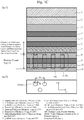
- Fig. 1A (a-1) and 1A(a-2) illustrate the structure (cross-sectional view and a plan view, respectively) of an AlGaN-based deep ultraviolet LED having a design wavelength ⁇ of 280 nm, as a deep ultraviolet LED in accordance with the first embodiment of the present invention.
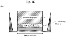
- Fig. 1B(b) illustrates a deep ultraviolet LED mounted in in a surface-mount package.
- the deep ultraviolet LED includes, sequentially from the top of the cross-sectional view in Fig. 1A (a-1), a sapphire substrate 1, an AlN buffer layer 2, an n-AlGaN layer 3, a barrier layer 4, a quantum well layer 5, a barrier layer 6, a multi-quantum barrier layer (MQB) 7, a p-AlGaN layer (transparent p-AlGaN layer) 8, a p-GaN contact layer 9, a Ni layer 10, and an Au reflecting electrode layer 11.
- MQB multi-quantum barrier layer
- the thickness of the p-AlGaN layer 8 is less than or equal to 100 nm, and a photonic crystal periodic structure 100 is provided in a region including the interface between the p-GaN contact layer 9 and the p-AlGaN layer 8 such that the photonic crystal periodic structure 100 does not extend beyond the p-AlGaN layer in the direction of the substrate.
- the photonic crystal periodic structure 100 is a reflecting photonic crystal periodic structure that is designed to reflect light with the wavelength ⁇ by having voids (columnar structures or holes) 101(h) and thus having a photonic band gap.
- the photonic crystal periodic structure is formed within only the p-GaN contact layer 9, light will be undesirably absorbed by the p-GaN contact layer.
- the multi-quantum barrier layer (MQB) 7 may also be an electron blocking layer. This is also true of the following embodiments.
- the reflecting photonic crystal periodic structure 100 has hole structures in which the voids 101(h) each having a columnar shape or the like, having a lower refractive index than those of the p-AlGaN layer and p-GaN contact layer, such as the air, and having a circular cross-section with a radius R, are formed in a triangular lattice pattern with a period of a along the x-direction and the y-direction.
- the voids 101(h) are structures that do not extend beyond the interface between the p-AlGaN layer 8 and the multi-quantum barrier layer 7.
- the distance G from end faces of the voids 101(h) in the direction of the substrate to the quantum well layer 5 is greater than or equal to the total thickness of the barrier layer 6 and the multi-quantum barrier layer 7 and less than or equal to 80 nm.
- the depth h of the reflecting photonic crystal periodic structure 100 is less than or equal to the total thickness of the p-AlGaN layer 8 and the p-GaN contact layer 9.
- TE light and TM light of deep ultraviolet light with a wavelength ⁇ emitted from the quantum well layer 5 are radiated in all directions and propagate through the medium while being elliptically polarized.
- the photonic crystal periodic structure 100 provided around the quantum well layer 5 is formed as two structures, which are the p-AlGaN layer 8 and the air, having different refractive indices on an end face.
- a photonic band gap (PBG) for TM light was not observed, while as illustrated in Fig. 2(b) , a large PBG for TE light was observed between a first photonic band ( ⁇ 1TE) and a second photonic band ( ⁇ 2TE).
- PBG photonic band gap
- the photonic crystals are located closer to the quantum well layer, it becomes unnecessary to set the depths of the photonic crystals to 300 nm even when the period is 300 nm as described in Earlier Technology 1 or the like, and a reflection effect that is greater than or equal to the reflection effect of the structure of Earlier Technology 1 or the like can be obtained even when the depths of the photonic crystals are as shallow as about 60 nm. Further, the range of the order m that can be taken is increased. It should be noted that the smaller the m, the smaller the period.
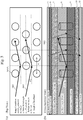
- Figs. 3 illustrate views of the reflection effect of the photonic crystals.
- TE light that has entered the photonic crystal periodic structure provided around the quantum well layer from all directions is scattered within the plane and is reflected in the direction of the substrate as indicated by AR1 because the light completely satisfies the Bragg scattering condition.
- TM light will not be Bragg-scattered in the depth direction as indicated by a dashed line AR2 as there is no PBG for the TM light.
- the incident light will not be absorbed by the p-GaN contact layer or will not disappear.
- the deep ultraviolet LED in this embodiment it is possible to, by devising the position of the photonic crystal periodic structure provided in a target layer to be provided with the photonic crystal periodic structure, suppress the cloudiness of the crystal-forming layer without increasing the thickness thereof and increase the reflection effect, and thus obtain high light extraction efficiency.
- Figs. 4A (a-1) and 4A(a-2) are illustrated in accordance with the second embodiment of the present invention.
- Fig. 4A (a-1) is a cross-sectional view and 4A(a-2) is a plan view.
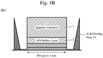
- Fig. 4B(b) illustrates a deep ultraviolet LED mounted in a surface-mount package.
- the deep ultraviolet LED includes, sequentially from the top of Fig.
- a-1 a sapphire substrate 1, an AlN buffer layer 2, an n-AlGaN layer 3, a barrier layer 4, a quantum well layer 5, a barrier layer 6, a multi-quantum barrier layer (MQB) 7, a p-AlGaN contact layer (transparent p-AlGaN contact layer) 8a, an ultrathin Ni layer 10a, and an A1 reflecting electrode layer 11 a.
- MQB multi-quantum barrier layer
- the thickness of the p-AlGaN contact layer 8a is less than or equal to 100 nm, and the photonic crystal periodic structure 100 is provided within the p-AlGaN contact layer 8a in a region in which the photonic crystal periodic structure 100 does not extend beyond the p-AlGaN layer in the direction of the substrate.
- the photonic crystal periodic structure 100 is a reflecting photonic crystal periodic structure that is designed to reflect light with the wavelength ⁇ by having voids (columnar structures or holes) 101(h) and thus having a photonic band gap.
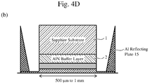
- Figs. 4C (a-1), 4C(a-2), and 4D(b) illustrate modified examples of Figs. 4A (a-1), 4A(a-2), and 4B(b).
- This structure is the one in which the depths of the voids of the photonic crystal periodic structure in the thickness direction are extended in the direction opposite to the substrate such that the voids reach the reflecting electrode layer by penetrating the ultrathin metal layer, but do not penetrate the reflecting electrode layer.
- the other details of the photonic crystal periodic structure and observation of the views of TE light and TM light from the photonic band structure using the plane wave expansion method are the same as those in the first embodiment.
- light that has entered the photonic crystal periodic structure is scattered within the plane and is reflected in the direction of the substrate. Therefore, the light will not be absorbed by the A1 reflecting electrode (with a reflectivity of 90 %) or will not disappear.
- Figs. 5 illustrate a computation model (first embodiment) of the photonic crystals in the p-GaN contact layer
- Figs. 6 illustrate a computation model (second embodiment) of the p-AlGaN contact layer.
- Fig. 7A illustrates a computation model of the pGaN contact.
- Fig. 7A (a-2) illustrates the analysis results and a radiation pattern.
- Fig. 7A(b) illustrates the details of the model and the light extraction efficiency that is analysis result.
- Fig. 7A (c-1) illustrates a computation model of the pAlGaN contact.
- Fig. 7A (c-2) illustrates the analysis results and a radiation pattern.
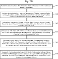
- Fig. 7B is a detailed process flow chart for determining the relationship between the size of the photonic band gap and the reflection/transmission effect as well as the rate of change of the light extraction efficiency (LEE) of the deep ultraviolet LED through analysis using the FDTD method, and obtaining the diameter d, the period a, and the depth h of the photonic crystals with which the LEE rate of change becomes maximum.
- LEE light extraction efficiency
- the ratio (R/a) of the period a and the radius R of the structure, which are parameters of the period structure, is tentatively determined.
- the refractive indices n 1 and n 2 of the structure are computed, and the average refractive index n av is computed from them and R/a, and then, the value is substituted into the formula of the Bragg condition to obtain the period a and the radius R for each order m.
- a photonic band structure for TE light is analyzed with the plane wave expansion method using R/a, the wavelength ⁇ , and the dielectric constants ⁇ 1 and ⁇ 2 of the structure obtained from the respective refractive indices n 1 and n 2 .
- R/a with which the PBG between the first photonic band and the second photonic band for TE light becomes maximum is determined through analysis that is repeatedly performed by changing the tentatively determined R/a value.
- the light extraction efficiency for light with the wavelength ⁇ is determined through a simulation analysis using the FDTD method that is performed by using as variables the individual period a and radius R corresponding to each order m of the Bragg condition and the depth h of a given period structure.
- Simulation using the FDTD method is repeatedly performed so as to determine the order m of the Bragg condition with which the light extraction efficiency for light with the wavelength ⁇ becomes maximum, as well as the period a, the radius R, and the depth h that are the parameters of the period structure corresponding to the order m.
- Tables 1 and 2 show the analysis results.
- Table 2 illustrates the analysis results of LEE when the order m is changed.
- pAlGaN photonic crystals in the p-AlGaN contact layer
- pGaN photonic crystals in the p-GaN contact layer
- Flat a structure without a photonic crystal periodic structure
- PhC Depth 40 nm the depths of the voids are 40 nm
- Power the output value of the FDTD method
- Flat LEE% the LEE value computed with the ray-tracing method
- Enhanced the LEE rate of change of the PhC output value relative to the output value of Flat
- PhC LEE% LEE% of photonic crystals that is Flat LEE% ⁇ (Enhanced+100%)
- G50 nm the distance from end faces of the voids to the quantum well layer is 50 nm
- Diameter the diameters of the voids
- Period the period of the photonic crystals.
- Figs. 8A are views illustrating electric field distribution Ex components; specifically, Fig. 8A(a) illustrates Flat, Fig. 8A(b) illustrates a photonic crystal periodic structure (the photonic crystal periodic structure is not illustrated), and Fig. 8A(c) illustrates a photonic crystal periodic structure (the photonic crystal periodic structure is illustrated). Each figure illustrates an electric field distribution in the cross-sectional structure. It should be noted that the photonic crystal periodic structure is omitted in Figs. 8A(c) and 8A(b) for clarification purposes.
- the results can verify that in the structure provided with a photonic crystal periodic structure, the reflection effect of the photonic crystals is obtained in the portion between the p-GaN contact layer and the Ni layer.
- a phenomenon similar to that of the Ex components in Figs. 8A are observed (see regions A3 and A4).
- Fig. 8D(a) illustrates an electric field distribution Etotal of Flat
- Fig. 8D(b) illustrates an electric field distribution Etotal of the center portion of the photonic crystals.
- an electric field propagates outward through repetition of high and low levels (shown by the gray scale of the color).
- the analysis results clearly illustrate a physical phenomenon that "TE light that has entered the photonic crystal periodic structure provided around the quantum well layer from all directions is scattered within the plane and is reflected in the direction of the substrate because the light completely satisfies the Bragg scattering condition" as has been described with reference to Figs. 3 .
- Figs. 9 illustrate the results of analyzing the LEE rate of change using the FDTD method.
- Fig. 9(a) illustrates the LEE rate of change of the photonic crystals in the p-AlGaN contact layer
- Fig. 9(b) illustrates the LEE rate of change of the photonic crystals in the p-GaN contact layer.
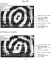
- FIG. 9(c) illustrates radiation patterns of the photonic crystal periodic structure in the p-GaN contact layer when the distance to the quantum well layer is 60 nm and the depths of the voids are 60 nm, and Flat of the layer, and similarly, radiation patterns of the photonic crystal periodic structure in the p-AlGaN contact layer and Flat of the layer.
- an output value in the front direction is particularly increased in comparison with that of Flat.
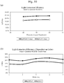
- Figs. 10 illustrate the results of analyzing the light extraction efficiency (LEE) obtained through cross simulation based on the FDTD method and the ray-tracing method.
- Fig. 10(a) illustrates the light extraction efficiency of the photonic crystals provided in the p-GaN contact layer and the p-AlGaN contact layer when the distance to the quantum well layer is 60 nm. From the results, a proportional relationship between the depth h of the photonic crystal periodic structure (holes) and the LEE is observed.
- the aforementioned results can confirm that according to an embodiment of the present invention, as the photonic crystal periodic structure is located closer to the quantum well structure, the reflection effect of the photonic crystal periodic structure can be increased double in the case of the photonic crystal periodic structure provided in the p-AlGaN contact layer, and the light extraction efficiency of the photonic crystal periodic structure can be increased more than three times in the case of the photonic crystal periodic structure provided in the p-GaN contact layer.
- FIGS. 11 are views illustrating an exemplary process of forming a photonic crystal periodic structure.
- the nanoimprint lithography technique is used for forming photonic crystals.
- a resin mold 200 is used for the mold.
- bi-layer resist is used in order to perform dry etching in a direction close to vertical and accurately retain the diameters of holes.
- lower-layer resist 211 is formed on the surface of the p-GaN contact layer 209 through spin coating.
- Si-containing upper-layer resist 210 is formed thereon through spin coating to form bi-layer resist (see Fig. 11(a) ).
- the resin mold 200 having an inverted pattern of a predetermined photonic crystal periodic structure is pressed against the upper-layer resist, and is UV curing is performed to imprint a photonic crystal pattern 212 to the upper-layer resist 210 (see Fig. 11(b) ).
- the upper-layer resist 210 is etched with oxygen plasma to form a mask 213. See Fig. 11(c) .
- the mask 213 is etched with ICP plasma up to a position where the distance from an end face of the photonic crystal pattern (holes) 212 to the quantum well layer 205 becomes greater than or equal to the total thickness of the barrier layer 206 and the multi-quantum barrier layer 207 and less than or equal to 80 nm, which is also a position where the holes do not extend beyond the p-AlGaN layer 208, so that the depths of the holes are less than or equal to the total thickness of the p-AlGaN layer 208 and the p-GaN contact layer 209. See Fig. 11(d) . Finally, the remaining lower-layer resist 211 is washed to obtain a clean surface.
- a photonic crystal pattern is formed after a p-GaN contact layer or a p-AlGaN contact layer is formed, and then, a metal layer and a reflecting electrode layer are formed thereon using oblique deposition, so that a structure illustrated in Figs. 16A or 19A is formed.
- a metal layer and a reflecting electrode layer can be stacked on the surface of the p-GaN contact layer or the p-AlGaN contact layer without the metal layer and the reflecting electrode layer formed in the holes of the photonic crystal pattern.
- a structure of an AlGaN-based deep ultraviolet LED with a design wavelength ⁇ of 280 nm is represented in Fig. 12A (a-1) and 12A(a-2).
- Fig. 12A (a-1) is a cross-sectional view and Fig. 12A (a-2) is a plan view.
- Fig. 12B(b) is a deep ultraviolet LED mounted in a surface-mount package.
- This LED has the same structure as the stacked thin-film structure of the deep ultraviolet LED in the first embodiment, but is different in that the thickness of the p-GaN contact layer 9 is 200 nm. This is in order to obtain a planar surface by stacking a thick p-GaN contact layer in the device production process.
- the photonic crystal periodic structure 100 is provided in a region including the interface between the p-GaN contact layer 9 and the p-AlGaN layer 8 such that the photonic crystal periodic structure 100 does not extend beyond the p-AlGaN layer in the direction of the substrate.
- the photonic crystal periodic structure 100 is a reflecting photonic crystal periodic structure that is designed to reflect light with the wavelength ⁇ by having voids (columnar structures or holes) 101(h) and thus having a photonic band gap.
- the voids 101(h) are structures that do not extend beyond the interface between the p-AlGaN layer 8 and the multi-quantum barrier layer 7.
- the distance G from end faces of the voids 101(h) in the direction of the substrate to the quantum well layer 5 is greater than or equal to the total thickness of the barrier layer 6 and the multi-quantum barrier layer 7 and less than or equal to 80 nm.
- the depth h of the reflecting photonic crystal periodic structure 100 is less than or equal to the total thickness of the p-AlGaN layer 8 and the p-GaN contact layer 9.
- FIG. 13 illustrates a photonic crystal computation model of the p-GaN contact layer.
- Fig. 14(a) Enhancement of LEE
- Fig. 14(b) light extraction efficiency
- Fig. 14(c) radiation patterns.
- a maximum value which is greater than or equal to 2.5 times that of Flat, is obtained at all depths in the range of a distance of 50 nm from end faces of the voids to the quantum well layer.
- a structure provided with a photonic crystal periodic structure has an increased output value in the front direction (at an angle of 0 to 10°) relative to that of Flat.
- the efficiency is slightly decreased as the depths of the photonic crystals are greater.
- electric field intensity distributions in cross-sections of photonic crystals with depths of 120 nm, 140 nm, and 160 nm were compared.
- Fig. 15A illustrates an electric field intensity distribution in a cross-section of the photonic crystals with a depth of 120 nm.
- Fig. 15B illustrates an electric field intensity distribution in a cross-section of the photonic crystals with a depth of 140 nm.
- Fig. 15C illustrates an electric field intensity distribution in a cross-section of the photonic crystals with a depth of 160 nm. From Figs. 15A to 15C (electric field intensity distributions), it is seen that light (electric field) that has entered the photonic crystals with all depths reaches the deepest portions of the photonic crystals. This is considered to be due to the reason that as the photonic crystals have greater depths, light (electric field) enters the p-GaN contact layer, and the light is absorbed therein and thus disappears.
- the thickness of the p-GaN contact layer is preferably thinner so that the photonic crystals can have small depths.
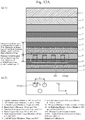
- Figs. 16A (a-1) and 16A(a-2) illustrate the structure of an AlGaN-based deep ultraviolet LED with a design wavelength ⁇ of 280 nm as a deep ultraviolet LED in accordance with the fifth embodiment of the present invention.
- Fig. 16A (a-1) is a cross-sectional view and Fig. 16A (a-2) is a plan view.
- Fig. 16B(b) illustrates a deep ultraviolet LED mounted in a surface-mount package.
- This LED has the same structure as the stacked thin-film structure of the deep ultraviolet LED in the fourth embodiment, but is different in that the thickness of the p-GaN contact layer 9 is 150 nm. This is a modified example seen from a perspective of using another method in the device production process.
- the photonic crystal periodic structure 100 is provided in a region including the interface between the p-GaN contact layer 9 and the p-AlGaN layer 8 such that the photonic crystal periodic structure 100 does not extend beyond the p-AlGaN layer in the direction of the substrate.
- the photonic crystal periodic structure 100 is a reflecting photonic crystal periodic structure that is designed to reflect light with the wavelength ⁇ by having voids (columnar structures or holes) 101(h) and thus having a photonic band gap.
- the voids 101(h) have structures in which the voids do not extend beyond the interface between the p-AlGaN layer 8 and the multi-quantum barrier layer 7 but reach the interface between the p-GaN contact layer 9 and the Ni layer 10.
- the distance G from end faces of the voids 101(h) in the direction of the substrate to the quantum well layer 5 is greater than or equal to the total thickness of the barrier layer 6 and the multi-quantum barrier layer 7 and less than or equal to 80 nm.
- the depth h of the reflecting photonic crystal periodic structure 100 is less than or equal to the total thickness of the p-AlGaN layer 8 and the p-GaN contact layer 9.
- FIG. 17 illustrate a photonic crystal computation model of the p-GaN contact layer.
- Fig. 18(a) Enhancement of LEE
- Fig. 18(b) light extraction efficiency
- Fig. 18(c) radiation patterns.
- a maximum value which is greater than or equal to 2.5 times that of Flat, is obtained at a distance of 60 nm from the quantum well layer 5. Meanwhile, regarding the light extraction efficiency in Fig. 18(b) , a maximum value of 15.7 % is obtained. Further, regarding the radiation patterns, an output on the axis (0 to 10°) is increased relative to that of Flat.
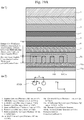
- Figs. 19A (a-1) and 19A(a-2) illustrate the structure of an AlGaN-based deep ultraviolet LED with a design wavelength ⁇ of 280 nm as a deep ultraviolet LED in accordance with the sixth embodiment of the present invention.
- Fig. 19A (a-1) is a cross-sectional view and Fig. 19A (a-2) is a plan view.
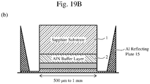
- Fig. 19B(b) is a deep ultraviolet LED mounted in a surface-mount package.
- the LED has the same structure as the stacked thin-film structure of the deep ultraviolet LED in the second embodiment, but is a modified example seen from a perspective of using another method in the device production process.
- the thickness of the p-AlGaN contact layer 8a is less than or equal to 100 nm, and the photonic crystal periodic structure 100 is provided in a region within the p-AlGaN contact layer 8a such that the photonic crystal periodic structure 100 does not extend beyond the p-AlGaN contact layer in the direction of the substrate.
- the photonic crystal periodic structure 100 is a reflecting photonic crystal periodic structure that is designed to reflect light with the wavelength ⁇ by having voids (columnar structures or holes) 101(h) and thus having a photonic band gap.
- the voids 101(h) have structures in which the voids 101(h) do not extend beyond the interface between the p-AlGaN contact layer 8a and the multi-quantum barrier layer 7 but reach the interface between the p-AlGaN contact layer 8a and the ultrathin Ni layer 10a.
- the distance G of from end faces of the voids 101(h) in the direction of the substrate to the quantum well layer 5 is greater than or equal to the total thickness of the barrier layer 6 and the multi-quantum barrier layer 7 and less than or equal to 80 nm.
- the depth h of the reflecting photonic crystal periodic structure 100 is less than or equal to the thickness of the p-AlGaN contact layer 8a.
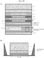
- FIG. 20 illustrate a photonic crystal computation model of the p-AlGaN contact layer.
- FIG. 21(a) Enhancement of LEE
- Fig. 21(b) LEE
- Fig. 21(c) radiation patterns.
- Figs. 22A (a-1) and 22A(a-2) illustrate the structure of an AlGaN-based deep ultraviolet LED with a design wavelength ⁇ of 280 nm as a deep ultraviolet LED in accordance with the seventh embodiment of the present invention.
- Fig. 22A (a-1) is a cross-sectional view and Fig. 22A (a-2) is a plan view.
- Fig. 22B(b) is a deep ultraviolet LED mounted in a surface-mount package.
- the LED has the same structure as the stacked thin-film structures of the deep ultraviolet LEDs in the first and forth embodiments, but is different in the position where the photonic crystal periodic structure 100 is provided. This is a modified example seen from a perspective of using another method in the device production process.
- the photonic crystal periodic structure 100 is provided in a region within the thickness of the p-GaN contact layer 9 such that the photonic crystal periodic structure 100 does not extend beyond the interface between the p-GaN contact layer 9 and the p-AlGaN layer 8 in the direction of the substrate.
- the photonic crystal periodic structure 100 is a reflecting photonic crystal periodic structure that is designed to reflect light with the wavelength ⁇ by having voids (columnar structures or holes) 101(h) and thus having a photonic band gap.
- the voids 101(h) are provided such that they do not extend beyond the interface between the p-GaN contact layer 9 and the Ni layer 10.
- the distance G from end faces of the voids 101(h) in the direction of the substrate to the quantum well layer 5 is greater than or equal to the total thickness of the barrier layer 6 and the multi-quantum barrier layer 7 and less than or equal to 80 nm.
- the depth h of the reflecting photonic crystal periodic structure 100 is less than or equal to the thickness of the p-GaN contact layer 9.
- TE light and TM light of deep ultraviolet light with a wavelength ⁇ emitted from the quantum well layer 5 are radiated in all directions and propagate through the medium while being elliptically polarized.
- the photonic crystal periodic structure 100 provided around the quantum well layer 5 is provided within the thickness of the p-GaN contact layer 9. Therefore, the photonic crystal periodic structure 100 is formed as a structure having two different refractive indices, which are the p-GaN contact layer 9 and the air, at an end face thereof.
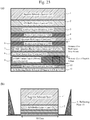
- FIG. 23 illustrate a photonic crystal computation model of the LED structure.
- the computation model was designed such that the thickness of the p-AlGaN layer 8 was changed in increments of 10 nm in the range of 0 to 30 nm, and the positions of the voids 101(h) were set such that end faces of the voids in the direction of the substrate had depths of 120 nm from the interface between the p-AlGaN layer 8 and the p-GaN contact layer 9.
- the thinner the p-AlGaN layer 8 the shorter the distance G between the quantum well layer 5 and the end faces of the voids 101(h) in the direction of the substrate. That is, the computation model was designed such that the distance G became 50 nm when the thickness of the p-AlGaN layer 8 was 0 nm, and the thickness of the p-AlGaN layer 8 was changed in increments of 10 nm so that the distance G similarly became 80 nm when the thickness of the p-AlGaN layer 8 was 30 nm.
- the analysis results are shown in Table 6, Fig. 24(a) : Enhancement of LEE, Fig. 24(b) : light extraction efficiency, and Fig.
- a maximum value which is about 2.7 times as high, is obtained at a distance G of 50 nm from the quantum well layer 5 (the thickness of the p-AlGaN layer in this case is 0 nm), and an intensity, which is about 2.5 times as high, is also obtained at a distance G of 60 nm (likewise, the thickness of the p-AlGaN layer is 10 nm).
- a maximum value of 17.3% is obtained at a distance G of 50 nm.
- Fig. 24(c) illustrates radiation patterns at a distance G of 50 nm. It is found that an output in the axial direction (0 to 30°) is increased relative to that of Flat.
- an LED device is formed.
- the LEE of the deep ultraviolet LED can be drastically improved by providing a photonic crystal periodic structure in a thin p-AlGaN layer.
- each element of the present invention can be freely selected, and an invention that includes the selected element is also included in the present invention.
- the present application is applicable to deep ultraviolet LEDs.
Landscapes
- Led Devices (AREA)
Abstract
Description
- The present invention relates to a technology of an AlGaN-based deep ultraviolet LED.
- A deep ultraviolet LED with a light emission wavelength of less than or equal to 280 nm is attracting attention as an alternative technology for mercury germicidal lamps in a variety of fields of application, such as sterilization, water purification, air purification, and medical care. However, the wall-plug efficiency (WPE) of a LED is as low as several %, which is significantly lower than a wall-plug efficiency of 20% of a mercury lamp. This is mainly because greater than or equal to 50 % of the emitted light is absorbed by a p-GaN contact layer, with the result that the light extraction efficiency (LEE) becomes as low as about 6 %.
- According to
Patent Literature 1, photonic crystals are provided in the thickness direction in a region including an interface between a p-GaN contact layer and a p-AlGaN layer, so that incident light is reflected and the aforementioned absorption is suppressed. - Patent Literature 1:
JP 5757512 B - However, the photonic crystals described in
Patent Literature 1 cannot obtain an effective reflection effect unless the depths of the photonic crystals are about 300 nm that is equal to the period of the photonic crystals. To that end, the total thickness of the p-GaN contact layer and the p-AlGaN layer needs to be greater than or equal to 300 nm or the thickness of the p-AlGaN contact layer needs to be greater than or equal to 300 nm. - Nevertheless, if the p-AlGaN layer is formed to a thickness of 300 nm, problems would arise such that the layer becomes cloudy and sufficient transparency cannot be obtained, with the result that the LEE decreases.
- It is an object of the present invention to provide a novel technique of increasing the light extraction efficiency of a deep ultraviolet LED.
- According to a first aspect of the present invention, there is provided a deep ultraviolet LED with a design wavelength λ, including, sequentially arranged from a side opposite to a substrate, a reflecting electrode layer, a metal layer, a p-GaN contact layer, a p-AlGaN layer that is transparent to light with the wavelength λ, one of a multi-quantum barrier layer or an electron blocking layer, a barrier layer, and a quantum well layer. A thickness of the p-AlGaN layer is less than or equal to 100 nm; a reflecting photonic crystal periodic structure having a plurality of voids is provided in a region in a thickness direction including at least an interface between the p-GaN contact layer and the p-AlGaN layer such that the reflecting photonic crystal periodic structure does not extend beyond the p-AlGaN layer in a direction of the substrate; maximum light extraction efficiency is obtained when a distance from end faces of the voids in the direction of the substrate to the quantum well layer is greater than or equal to a total thickness of the barrier layer and the one of the multi-quantum barrier layer or the electron blocking layer and less than or equal to 80 nm, and a depth h of each void is less than or equal to a total thickness of the p-AlGaN layer and the p-GaN contact layer; the reflecting photonic crystal periodic structure has a photonic band gap that opens for TE polarized components; a period a of the photonic crystal periodic structure satisfies a Bragg condition with respect to light with the design wavelength λ; an order m in a formula of the Bragg condition satisfies 1≤m≤5; and provided that a radius of each void is R, R/a with which the photonic band gap becomes maximum is satisfied.
- According to a second aspect of the present invention, there is provided a deep ultraviolet LED with a design wavelength λ, including, sequentially arranged from a side opposite to a substrate, a reflecting electrode layer, an ultrathin metal layer, a p-AlGaN contact layer that is transparent to light with the wavelength λ, a multi-quantum barrier layer (or an electron blocking layer), a barrier layer, and a quantum well layer. A thickness of the p-AlGaN contact layer is less than or equal to 100 nm; a reflecting photonic crystal periodic structure having a plurality of voids is provided within the p-AlGaN contact layer in a region in a thickness direction where the reflecting photonic crystal periodic structure does not extend beyond the p-AlGaN contact layer in a direction of the substrate; maximum light extraction efficiency is obtained when a distance from end faces of the voids in the direction of the substrate to the quantum well layer is greater than or equal to a total thickness of the barrier layer and the multi-quantum barrier layer (or the electron blocking layer) and less than or equal to 80 nm, and when a depth h of each void is less than or equal to the thickness of the p-AlGaN contact layer; the reflecting photonic crystal periodic structure has a photonic band gap that opens for TE polarized components; a period a of the photonic crystal periodic structure satisfies a Bragg condition with respect to light with the design wavelength λ; an order m in a formula of the Bragg condition satisfies 1≤m≤5; and provided that a radius of each void is R, R/a with which the photonic band gap becomes maximum is satisfied.
- According to a third aspect of the present invention, there is provided a deep ultraviolet LED with a design wavelength λ, including, sequentially arranged from a side opposite to a substrate, a reflecting electrode layer, a metal layer, a p-GaN contact layer, a p-AlGaN layer that is transparent to light with the wavelength λ, a multi-quantum barrier layer (or an electron blocking layer), a barrier layer, and a quantum well layer. A thickness of the p-AlGaN layer is less than or equal to 100 nm; a reflecting photonic crystal periodic structure having a plurality of voids is provided in a region including at least an interface between the p-GaN contact layer and the p-AlGaN layer such that the reflecting photonic crystal periodic structure does not extend beyond the p-AlGaN layer in a direction of the substrate, penetrates the p-GaN contact layer and the metal layer from a thickness direction, and reaches an inside of the reflecting electrode layer but does not extend beyond the reflecting electrode layer; maximum light extraction efficiency is obtained when a distance from end faces of the voids in the direction of the substrate to the quantum well layer is greater than or equal to a total thickness of the barrier layer and the multi-quantum barrier layer (or the electron blocking layer) and less than or equal to 80 nm; the reflecting photonic crystal periodic structure has a photonic band gap that opens for TE polarized components; a period a of the photonic crystal periodic structure satisfies a Bragg condition with respect to light with the design wavelength λ; an order m in a formula of the Bragg condition satisfies 1≤m≤5; and provided that a radius of each void is R, R/a with which the photonic band gap becomes maximum is satisfied.
- According to a forth aspect of the present invention, there is provided a deep ultraviolet LED with a design wavelength λ, including, sequentially arranged from a side opposite to a substrate, a reflecting electrode layer, an ultrathin metal layer, a p-AlGaN contact layer that is transparent to light with the wavelength λ, a multi-quantum barrier layer (or an electron blocking layer), a barrier layer, and a quantum well layer. A thickness of the p-AlGaN contact layer is less than or equal to 100 nm; a reflecting photonic crystal periodic structure having a plurality of voids is provided at a position where the reflecting photonic crystal periodic structure does not extend beyond the p-AlGaN contact layer in a direction of the substrate, penetrates the ultrathin metal layer from a thickness direction, and reaches an inside of the reflecting electrode layer but does not extend beyond the reflecting electrode layer; maximum light extraction efficiency is obtained when a distance from end faces of the voids in the direction of the substrate to the quantum well layer is greater than or equal to a total thickness of the barrier layer and the multi-quantum barrier layer (or the electron blocking layer) and less than or equal to 80 nm; the reflecting photonic crystal periodic structure has a photonic band gap that opens for TE polarized components; a period a of the photonic crystal periodic structure satisfies a Bragg condition with respect to light with the design wavelength λ; an order m in a formula of the Bragg condition satisfies 1≤m≤5; and provided that a radius of each void is R, R/a with which the photonic band gap becomes maximum is satisfied.
- According to a fifth aspect of the present invention, there is provided a deep ultraviolet LED with a design wavelength λ, including, sequentially arranged from a side opposite to a substrate, a reflecting electrode layer, a metal layer, a p-GaN contact layer, a p-AlGaN layer that is transparent to light with the wavelength λ, a multi-quantum barrier layer (or an electron blocking layer), a barrier layer, and a quantum well layer. A thickness of the p-AlGaN layer is less than or equal to 100 nm; a reflecting photonic crystal periodic structure having a plurality of voids is provided in a region including at least an interface between the p-GaN contact layer and the p-AlGaN layer such that the reflecting photonic crystal periodic structure does not extend beyond the p-AlGaN layer in a direction of the substrate and reaches an interface between the p-GaN contact layer and the metal layer from a thickness direction; maximum light extraction efficiency is obtained when a distance from end faces of the voids in the direction of the substrate to the quantum well layer is greater than or equal to a total thickness of the barrier layer and the multi-quantum barrier layer (or the electron blocking layer) and less than or equal to 80 nm, and a depth h of each void is less than or equal to a total thickness of the p-AlGaN layer and the p-GaN contact layer; the reflecting photonic crystal periodic structure has a photonic band gap that opens for TE polarized components; a period a of the photonic crystal periodic structure satisfies a Bragg condition with respect to light with the design wavelength λ; an order m of a condition of the Bragg condition satisfies 1≤m≤5; and provided that a radius of each void is R, R/a with which the photonic band gap becomes maximum is satisfied.
- According to a sixth aspect of the present invention, there is provided a deep ultraviolet LED with a design wavelength λ, including, sequentially arranged from a side opposite to a substrate, a reflecting electrode layer, an ultrathin metal layer, a p-AlGaN contact layer that is transparent to light with the wavelength λ, a multi-quantum barrier layer (or an electron blocking layer), a barrier layer, and a quantum well layer. A thickness of the p-AlGaN contact layer is less than or equal to 100 nm; a reflecting photonic crystal periodic structure having a plurality of voids is provided within the p-AlGaN contact layer such that the reflecting photonic crystal periodic structure does not extend beyond the p-AlGaN contact layer in a direction of the substrate, and reaches an interface between the p-AlGaN contact layer and the ultrathin metal layer from a thickness direction; maximum light extraction efficiency is obtained when a distance from end faces of the voids in the direction of the substrate to the quantum well layer is greater than or equal to a total thickness of the barrier layer and the multi-quantum barrier layer (or the electron blocking layer) and less than or equal to 80 nm; the reflecting photonic crystal periodic structure has a photonic band gap that opens for TE polarized components; a period a of the photonic crystal periodic structure satisfies a Bragg condition with respect to light with the design wavelength λ; an order m in a formula of the Bragg condition satisfies 1≤m≤5; and provided that a radius of each void is R, R/a with which the photonic band gap becomes maximum is satisfied.
- According to a seventh aspect of the present invention, there is provided a deep ultraviolet LED with a design wavelength λ, including, sequentially arranged from a side opposite to a substrate, a reflecting electrode layer, a metal layer, a p-GaN contact layer, a p-AlGaN layer that is transparent to light with the wavelength λ, a multi-quantum barrier layer (or an electron blocking layer), a barrier layer, and a quantum well layer. A thickness of the p-AlGaN layer is less than or equal to 100 nm; a reflecting photonic crystal periodic structure having a plurality of voids is provided in a region within a thickness of the p-GaN contact layer in a direction of the substrate such that the reflecting photonic crystal periodic structure does not extend beyond an interface between the p-GaN contact layer and the p-AlGaN layer; maximum light extraction efficiency is obtained when a distance from end faces of the voids in the direction of the substrate to the quantum well layer is greater than or equal to a total thickness of the barrier layer and the multi-quantum barrier layer (or the electron blocking layer) and less than or equal to 80 nm, and a depth h of each void is less than or equal to the thickness of the p-GaN contact layer; the reflecting photonic crystal periodic structure has a photonic band gap that opens for TE polarized components; a period a of the photonic crystal periodic structure satisfies a Bragg condition with respect to light with the design wavelength λ; an order m in a formula of the Bragg condition satisfies 1≤m≤5; and provided that a radius of each void is R, R/a with which the photonic band gap becomes maximum is satisfied.
- According to an eighth aspect of the present invention, there is provided a method for producing the deep ultraviolet LED according to the aforementioned first aspect, including: preparing a stacked structure including, sequentially arranged from a side opposite to a substrate, a reflecting electrode layer, a metal layer, a p-GaN contact layer, and a p-AlGaN layer that is transparent to light with the wavelength λ; preparing a mold for forming a reflecting photonic crystal periodic structure, wherein: a thickness of the p-AlGaN layer is less than or equal to 100 nm, the reflecting photonic crystal periodic structure has a plurality of voids and is provided in a region in a thickness direction including at least an interface between the p-GaN contact layer and the p-AlGaN layer such that the reflecting photonic crystal periodic structure does not extend beyond the p-AlGaN layer in a direction of the substrate, and maximum light extraction efficiency is obtained when a distance from end faces of the voids in the direction of the substrate to the quantum well layer is greater than or equal to a total thickness of the barrier layer and the multi-quantum barrier layer (or the electron blocking layer) and less than or equal to 80 nm, and a depth h of each void is less than or equal to a total thickness of the p-AlGaN layer and the p-GaN contact layer; forming a resist layer on the stacked structure and imprinting a structure of the mold thereto; and sequentially etching the stacked structure using the resist layer as a mask, thereby forming the photonic crystal periodic structure.
- According to a ninth aspect of the present invention, there is provided a method for producing the deep ultraviolet LED according to the aforementioned second aspect, including: preparing a stacked structure including, sequentially arranged from a side opposite to a substrate, a reflecting electrode layer, an ultrathin metal layer, and a p-AlGaN contact layer that is transparent to light with the wavelength λ; preparing a mold for forming a reflecting photonic crystal periodic structure, wherein: a thickness of the p-AlGaN contact layer is less than or equal to 100 nm, the reflecting photonic crystal periodic structure has a plurality of voids and is provided in a region in a thickness direction within the p-AlGaN contact layer such that the reflecting photonic crystal periodic structure does not extend beyond the p-AlGaN layer in a direction of the substrate, and maximum light extraction efficiency is obtained when a distance from end faces of the voids in the direction of the substrate to the quantum well layer is greater than or equal to a total thickness of the barrier layer and the multi-quantum barrier layer (or the electron blocking layer) and less than or equal to 80 nm, and a depth h of each void is less than or equal to a thickness of the p-AlGaN contact layer; forming a resist layer on the stacked structure and imprinting a structure of the mold thereto; and sequentially etching the stacked structure using the resist layer as a mask, thereby forming the photonic crystal periodic structure.
- According to a tenth aspect of the present invention, there is provided a method for producing the deep ultraviolet LED according to the aforementioned third aspect, including: preparing a stacked structure including, sequentially arranged from a side opposite to a substrate, a reflecting electrode layer, a metal layer, a p-GaN contact layer, and a p-AlGaN layer that is transparent to light with the wavelength λ; preparing a mold for forming a reflecting photonic crystal periodic structure, wherein: a thickness of the p-AlGaN layer is less than or equal to 100 nm, the reflecting photonic crystal periodic structure has a plurality of voids and is provided in a region including at least an interface between the p-GaN contact layer and the p-AlGaN layer such that the reflecting photonic crystal periodic structure does not extend beyond the p-AlGaN layer in a direction of the substrate, penetrates the p-GaN contact layer and the metal layer from a thickness direction, and reaches an inside of the reflecting electrode layer, but does not extend beyond the reflecting electrode layer, and maximum light extraction efficiency is obtained when a distance from end faces of the voids in the direction of the substrate to the quantum well layer is greater than or equal to a total thickness of the barrier layer and the multi-quantum barrier layer (or the electron blocking layer) and less than or equal to 80 nm; forming a resist layer on the stacked structure and imprinting a structure of the mold thereto; sequentially etching the stacked structure using the resist layer as a mask, thereby forming the photonic crystal periodic structure; and re-depositing a reflecting electrode layer.
- According to an eleventh aspect of the present invention, there is provided a method for producing the deep ultraviolet LED according to the aforementioned forth aspect, including: preparing a stacked structure including, sequentially arranged from a side opposite to a substrate, a reflecting electrode layer, an ultrathin metal layer, and a p-AlGaN contact layer that is transparent to light with the wavelength λ; preparing a mold for forming a reflecting photonic crystal periodic structure, wherein: a thickness of the p-AlGaN contact layer is less than or equal to 100 nm, the reflecting photonic crystal periodic structure has a plurality of voids and is provided at a position where the reflecting photonic crystal periodic structure does not extend beyond the p-AlGaN contact layer in a direction of the substrate, penetrates the ultrathin metal layer from a thickness direction, and reaches an inside of the reflecting electrode layer but does not extend beyond the reflecting electrode layer, and maximum light extraction efficiency is obtained when a distance from end faces of the voids in the direction of the substrate to the quantum well layer is greater than or equal to a total thickness of the barrier layer and the multi-quantum barrier layer (or the electron blocking layer) and less than or equal to 80 nm; forming a resist layer on the stacked structure and imprinting a structure of the mold thereto; sequentially etching the stacked structure using the resist layer as a mask, thereby forming the photonic crystal periodic structure; and re-depositing a reflecting electrode layer.
- According to a twelfth aspect of the present invention, there is provided a method for producing the deep ultraviolet LED according to the aforementioned fifth aspect, including: preparing a stacked structure including, sequentially arranged from a side opposite to a substrate, a reflecting electrode layer, a metal layer, a p-GaN contact layer, and a p-AlGaN layer that is transparent to light with the wavelength λ; preparing a mold for forming a reflecting photonic crystal periodic structure, wherein: a thickness of the p-AlGaN layer is less than or equal to 100 nm, the reflecting photonic crystal periodic structure has a plurality of voids and is provided in a region including at least an interface between the p-GaN contact layer and the p-AlGaN layer such that the reflecting photonic crystal periodic structure does not extend beyond the p-AlGaN layer in a direction of the substrate and reaches an interface between the p-GaN contact layer and the metal layer from a thickness direction, and maximum light extraction efficiency is obtained when a distance from end faces of the voids in the direction of the substrate to the quantum well layer is greater than or equal to a total thickness of the barrier layer and the multi-quantum barrier layer (or the electron blocking layer) and less than or equal to 80 nm, and a depth h of each void is less than or equal to a total thickness of the p-AlGaN layer and the p-GaN contact layer; growing crystals in up to the p-GaN contact layer of the stacked structure, forming a resist layer thereon, and imprinting a structure of the mold thereto; sequentially etching the stacked structure using the resist layer as a mask, thereby forming the photonic crystal periodic structure; and sequentially depositing the metal layer and the reflecting electrode layer obliquely after forming the photonic crystal periodic structure.
- According to a thirteenth aspect of the present invention, there is provided a method for producing the deep ultraviolet LED according to the aforementioned sixth aspect, including: preparing a stacked structure including, sequentially arranged from a side opposite to a substrate, a reflecting electrode layer, an ultrathin metal layer, and a p-AlGaN contact layer that is transparent to light with the wavelength λ; preparing a mold for forming a reflecting photonic crystal periodic structure, wherein: a thickness of the p-AlGaN contact layer is less than or equal to 100 nm, the reflecting photonic crystal periodic structure has a plurality of voids and is provided within the p-AlGaN contact layer such that the reflecting photonic crystal periodic structure does not extend beyond the p-AlGaN contact layer in a direction of the substrate, and reaches an interface between the p-AlGaN contact layer and the ultrathin metal layer from a thickness direction, and maximum light extraction efficiency is obtained when a distance from end faces of the voids in the direction of the substrate to the quantum well layer is greater than or equal to a total thickness of the barrier layer and the multi-quantum barrier layer (or the electron blocking layer) and less than or equal to 80 nm, and a depth h of each void is less than or equal to a thickness of the p-AlGaN contact layer; growing crystals in up to the p-AlGaN contact layer of the stacked structure, forming a resist layer thereon, and imprinting a structure of the mold thereto; sequentially etching the stacked structure using the resist layer as a mask, thereby forming the photonic crystal periodic structure; and sequentially depositing the ultrathin metal layer and the reflecting electrode layer obliquely after forming the photonic crystal periodic structure.
- According to a fourteenth aspect of the present invention, there is provided a method for producing the deep ultraviolet LED according to the aforementioned seventh aspect, including: preparing a stacked structure including, sequentially arranged from a side opposite to a substrate, a reflecting electrode layer, a metal layer, a p-GaN contact layer, and a p-AlGaN layer that is transparent to light with the wavelength λ; preparing a mold for forming a reflecting photonic crystal periodic structure, wherein: a thickness of the p-AlGaN layer is less than or equal to 100 nm, the reflecting photonic crystal periodic structure has a plurality of voids and is provided in a region within a thickness of the p-GaN contact layer in a direction of the substrate such that the reflecting photonic crystal periodic structure does not extend beyond an interface between the p-GaN contact layer and the p-AlGaN layer, and maximum light extraction efficiency is obtained when a distance from end faces of the voids in the direction of the substrate to the quantum well layer is greater than or equal to a total thickness of the barrier layer and the multi-quantum barrier layer (or the electron blocking layer) and less than or equal to 80 nm, and a depth h of each void is less than or equal to the thickness of the p-GaN contact layer; growing crystals in up to the p-GaN contact layer of the stacked structure, forming a resist layer thereon, and imprinting a structure of the mold thereto; and sequentially etching the stacked structure using the resist layer as a mask, thereby forming the photonic crystal periodic structure.
- According to the present invention, the LEE of a deep ultraviolet LED can be drastically improved by providing a photonic crystal periodic structure in a thin p-AlGaN layer.
-
-
Figs. 1A (a-1) and 1A(a-2) are a cross-sectional view and a plan view, respectively, illustrating an exemplary structure of a deep ultraviolet LED for which p-GaN contact layer photonic crystals in accordance with the first embodiment of the present invention are used. -
Fig. 1B(b) is a view illustrating an exemplary structure of a surface-mount package for the structure of a deep ultraviolet LED for which the p-GaN contact layer photonic crystals in accordance with the first embodiment of the present invention are used. -
Figs. 1C are views illustrated as a modified example ofFigs. 1A . -
Fig. 1D is a view illustrated as a modified example ofFig. 1B . -
Figs. 2 are charts illustrating exemplary photonic band structures for TM light (Fig. 2(a) ) and TE light (Fig. 2(b) ) determined using the plane wave expansion method when the photonic crystal periodic structure satisfies the Bragg scattering condition (mλ/neff=2a, where neff is the equivalent refractive index, a is the period, and m is the order). -
Figs. 3 are a top view (a) and a cross-sectional view (b) illustrating the reflection effect of photonic crystals. -
Figs. 4A (a-1) and 4A(a-2) are a cross-sectional view and a plan view, respectively, illustrating an exemplary structure of a deep ultraviolet LED for which p-AlGaN contact layer photonic crystals in accordance with the second embodiment of the present invention are used. -
Fig. 4B(b) is a view illustrating an exemplary structure of a surface-mount package for the structure of a deep ultraviolet LED for which the p-AlGaN contact layer photonic crystals in accordance with the second embodiment of the present invention are used. -
Figs. 4C are views illustrated as a modified example ofFigs. 4A . -
Fig. 4D is a view illustrated as a modified example ofFig. 4B . -
Figs. 5 are views illustrating a computation model of the FDTD method when photonic crystals are used for a p-GaN contact layer. -
Figs. 6 are views illustrating a computation model of the FDTD method when photonic crystals are used for a p-AlGaN contact layer. -
Figs. 7A are views illustrating a computation model of the ray-tracing method and analysis results. -
Fig. 7B is a detailed process flow chart for determining the relationship between the size of a photonic band gap and the reflection/transmission effect as well as the rate of change of the light extraction efficiency (LEE) of a deep ultraviolet LED through analysis using the FDTD method, and obtaining the diameter d, the period a, and the depth h of photonic crystals with which the LEE rate of change becomes maximum. -
Figs. 8A are views illustrating an electric field distribution: x components around a photonic crystal; specifically,Fig. 8A(a) illustrates a computation result regarding Ex when the layer is Flat,Fig. 8A(b) illustrates a computation result regarding Ex when a photonic crystal periodic structure is provided, andFig. 8A(c) illustrates a computation result regarding Ex when a photonic crystal periodic structure is provided. -
Figs. 8B are views illustrating an electric field distribution: y components around a photonic crystal corresponding toFigs. 8A . -
Figs. 8C are views illustrating an electric field distribution: z components around a photonic crystal corresponding toFigs. 8A . -
Figs. 8D are views illustrating total components of an electric field distribution in a horizon plane that perpendicularly intersects the intermediate point of a photonic crystal void in the depth direction. -
Figs. 9 are views illustrating the results of analyzing the LEE rate of change using the FDTD. -
Figs. 10 are views illustrating the results of analyzing the LEE through cross simulation based on the FDTD method and the ray-tracing method. -
Figs. 11 are views illustrating an exemplary process of forming a photonic crystal periodic structure. -
Figs. 12A (a-1) and 12A(a-2) are a cross-sectional view and a plan view, respectively, illustrating an exemplary structure of a deep ultraviolet LED for which p-GaN contact layer photonic crystals in accordance with the fourth embodiment of the present invention are used. -
Fig. 12B(b) is a view illustrating an exemplary structure of a surface-mount package for the structure of a deep ultraviolet LED for which p-GaN contact layer photonic crystals in accordance with the fourth embodiment of the present invention are used. -
Figs. 13 are views illustrating a computation model of the FDTD method when p-GaN photonic crystals are used. -
Figs. 14 illustrate the analysis results of (a) enhancement of the LEE, (b) light extraction efficiency, and (c) radiation patterns. -
Fig. 15A illustrates an electric field intensity distribution in a cross-section of photonic crystals at a depth of 120 nm. -
Fig. 15B illustrates an electric field intensity distribution in a cross-section of photonic crystals at a depth of 140 nm. -
Fig. 15C illustrates an electric field intensity distribution in a cross-section of photonic crystals at a depth of 160 nm. -
Figs. 16A (a-1) and 16A(a-2) are a cross-sectional view and a plan view, respectively, illustrating an exemplary structure of a deep ultraviolet LED for which p-GaN contact layer photonic crystals in accordance with the fifth embodiment of the present invention are used. -
Fig. 16B(b) is a view illustrating an exemplary structure of a surface-mount package for the structure of a deep ultraviolet LED for which p-GaN contact layer photonic crystals in accordance with the fifth embodiment of the present invention are used. -
Figs. 17 are views illustrating a computation model of the FDTD method when p-GaN photonic crystals are used. -
Figs. 18 illustrate the analysis results of (a) enhancement of the LEE, (b) light extraction efficiency, and (c) radiation patterns. -
Figs. 19A (a-1) and 19A(a-2) are a cross-sectional view and a plan view, respectively, illustrating an exemplary structure of a deep ultraviolet LED for which p-AlGaN contact layer photonic crystals in accordance with the sixth embodiment of the present invention are used. -
Fig. 19B(b) is a view illustrating an exemplary structure of a surface-mount package for the structure of a deep ultraviolet LED for which p-AlGaN contact layer photonic crystals in accordance with the sixth embodiment of the present invention are used. -
Figs. 20 are views illustrating a computation model of the FDTD method when p-AlGaN photonic crystals are used. -
Figs. 21 illustrate the analysis results of (a) enhancement of the LEE, (b) light extraction efficiency, and (c) radiation patterns. -
Figs. 22A (a-1) and 22A(a-2) are a cross-sectional view and a plan view, respectively, illustrating an exemplary structure of a deep ultraviolet LED for which p-GaN contact layer photonic crystals in accordance with the seventh embodiment of the present invention are used. -
Fig. 22B(b) is a view illustrating an exemplary structure of a surface-mount package for the structure of a deep ultraviolet LED for which p-GaN contact layer photonic crystals in accordance with the seventh embodiment of the present invention are used. -
Figs. 23 are views illustrating a computation model of the FDTD method when p-GaN photonic crystals are used. -
Figs. 24 illustrate the analysis results of (a) enhancement of the LEE, (b) light extraction efficiency, and (c) radiation patterns. - Hereinafter, a deep ultraviolet LED in accordance with an embodiment of the present invention will be described in detail with reference to the drawings.
-
Fig. 1A (a-1) and 1A(a-2) illustrate the structure (cross-sectional view and a plan view, respectively) of an AlGaN-based deep ultraviolet LED having a design wavelength λ of 280 nm, as a deep ultraviolet LED in accordance with the first embodiment of the present invention.Fig. 1B(b) illustrates a deep ultraviolet LED mounted in in a surface-mount package. - Specifically, the deep ultraviolet LED includes, sequentially from the top of the cross-sectional view in
Fig. 1A (a-1), asapphire substrate 1, anAlN buffer layer 2, an n-AlGaN layer 3, abarrier layer 4, aquantum well layer 5, abarrier layer 6, a multi-quantum barrier layer (MQB) 7, a p-AlGaN layer (transparent p-AlGaN layer) 8, a p-GaN contact layer 9, aNi layer 10, and an Au reflectingelectrode layer 11. The thickness of the p-AlGaN layer 8 is less than or equal to 100 nm, and a photonic crystalperiodic structure 100 is provided in a region including the interface between the p-GaN contact layer 9 and the p-AlGaN layer 8 such that the photonic crystalperiodic structure 100 does not extend beyond the p-AlGaN layer in the direction of the substrate. The photonic crystalperiodic structure 100 is a reflecting photonic crystal periodic structure that is designed to reflect light with the wavelength λ by having voids (columnar structures or holes) 101(h) and thus having a photonic band gap. It should be noted that if the photonic crystal periodic structure is formed within only the p-GaN contact layer 9, light will be undesirably absorbed by the p-GaN contact layer. It should be also noted that the multi-quantum barrier layer (MQB) 7 may also be an electron blocking layer. This is also true of the following embodiments. - As illustrated as an xy plan view in
Fig. 1A (a-2), the reflecting photonic crystalperiodic structure 100 has hole structures in which the voids 101(h) each having a columnar shape or the like, having a lower refractive index than those of the p-AlGaN layer and p-GaN contact layer, such as the air, and having a circular cross-section with a radius R, are formed in a triangular lattice pattern with a period of a along the x-direction and the y-direction. The voids 101(h) are structures that do not extend beyond the interface between the p-AlGaN layer 8 and themulti-quantum barrier layer 7. In addition, the distance G from end faces of the voids 101(h) in the direction of the substrate to thequantum well layer 5 is greater than or equal to the total thickness of thebarrier layer 6 and themulti-quantum barrier layer 7 and less than or equal to 80 nm. Further, the depth h of the reflecting photonic crystalperiodic structure 100 is less than or equal to the total thickness of the p-AlGaN layer 8 and the p-GaN contact layer 9. - It should be noted that as a modified example of this embodiment seen from a perspective of using another method in the device production process, it is also possible to provide a structure in which the columnar structures 101(h) reach the inside of the Au reflecting
electrode layer 11 by penetrating theNi layer 10 but do not reach the interface between the Au reflectingelectrode layer 11 and the air, as illustrated inFigs. 1C (a-1), 1C(a-2), and 1D(b). - In the aforementioned structure, TE light and TM light of deep ultraviolet light with a wavelength λ emitted from the
quantum well layer 5 are radiated in all directions and propagate through the medium while being elliptically polarized. The photonic crystalperiodic structure 100 provided around thequantum well layer 5 is formed as two structures, which are the p-AlGaN layer 8 and the air, having different refractive indices on an end face. Provided that the ratio of the radius R of each void to the period a is R/a=0.4, the filling factor f of the photonic crystals is computed by the formula: f=2π/30.5×(R/a)2=0.58. - In addition, from the refractive index of the air: n1=1.0 the refractive index of p-AlGaN: n2=2.583, and f=0.58, the equivalent refractive index neff is computed by the formula: neff=(n2 2+(n1 2-n2 2)×f)0.5=1.838.
- Then, provided that the light emission wavelength λ=280 nm,
Figs. 2 are obtained by determining photonic band structures for TM light and TE light when the photonic crystal periodic structure satisfies the Bragg scattering condition (mλ/neff=2a, where neff is the equivalent refractive index, a is the period, and m is the order), using the plane wave expansion method. - As illustrated in
Fig. 2(a) , a photonic band gap (PBG) for TM light was not observed, while as illustrated inFig. 2(b) , a large PBG for TE light was observed between a first photonic band (ω1TE) and a second photonic band (ω2TE). - It should be noted that R/a=0.4 is a value adopted from the principle that "the magnitude of R/a, the size of a PBG, and the rate of change of the light extraction efficiency are all proportional with one another" invented by the inventors and described in the international application
PCT/JP2015/071453 - In this embodiment, as the photonic crystals are located closer to the quantum well layer, it becomes unnecessary to set the depths of the photonic crystals to 300 nm even when the period is 300 nm as described in
Earlier Technology 1 or the like, and a reflection effect that is greater than or equal to the reflection effect of the structure ofEarlier Technology 1 or the like can be obtained even when the depths of the photonic crystals are as shallow as about 60 nm. Further, the range of the order m that can be taken is increased. It should be noted that the smaller the m, the smaller the period. -
Figs. 3 illustrate views of the reflection effect of the photonic crystals. As illustrated inFigs. 3(a) and 3(b) , TE light that has entered the photonic crystal periodic structure provided around the quantum well layer from all directions is scattered within the plane and is reflected in the direction of the substrate as indicated by AR1 because the light completely satisfies the Bragg scattering condition. Meanwhile, TM light will not be Bragg-scattered in the depth direction as indicated by a dashed line AR2 as there is no PBG for the TM light. Thus, the incident light will not be absorbed by the p-GaN contact layer or will not disappear. - Thus, according to the deep ultraviolet LED in this embodiment, it is possible to, by devising the position of the photonic crystal periodic structure provided in a target layer to be provided with the photonic crystal periodic structure, suppress the cloudiness of the crystal-forming layer without increasing the thickness thereof and increase the reflection effect, and thus obtain high light extraction efficiency.
- Next, the structure of an AlGaN-based deep ultraviolet LED with a design wavelength λ of 280 nm is illustrated in
Figs. 4A (a-1) and 4A(a-2) as a deep ultraviolet LED in accordance with the second embodiment of the present invention.Fig. 4A (a-1) is a cross-sectional view and 4A(a-2) is a plan view.Fig. 4B(b) illustrates a deep ultraviolet LED mounted in a surface-mount package. Specifically, the deep ultraviolet LED includes, sequentially from the top ofFig. 4A (a-1), asapphire substrate 1, anAlN buffer layer 2, an n-AlGaN layer 3, abarrier layer 4, aquantum well layer 5, abarrier layer 6, a multi-quantum barrier layer (MQB) 7, a p-AlGaN contact layer (transparent p-AlGaN contact layer) 8a, anultrathin Ni layer 10a, and an A1 reflectingelectrode layer 11 a. - The thickness of the p-
AlGaN contact layer 8a is less than or equal to 100 nm, and the photonic crystalperiodic structure 100 is provided within the p-AlGaN contact layer 8a in a region in which the photonic crystalperiodic structure 100 does not extend beyond the p-AlGaN layer in the direction of the substrate. The photonic crystalperiodic structure 100 is a reflecting photonic crystal periodic structure that is designed to reflect light with the wavelength λ by having voids (columnar structures or holes) 101(h) and thus having a photonic band gap. -
Figs. 4C (a-1), 4C(a-2), and 4D(b) illustrate modified examples ofFigs. 4A (a-1), 4A(a-2), and 4B(b). This structure is the one in which the depths of the voids of the photonic crystal periodic structure in the thickness direction are extended in the direction opposite to the substrate such that the voids reach the reflecting electrode layer by penetrating the ultrathin metal layer, but do not penetrate the reflecting electrode layer. - The other details of the photonic crystal periodic structure and observation of the views of TE light and TM light from the photonic band structure using the plane wave expansion method are the same as those in the first embodiment. In this case, light that has entered the photonic crystal periodic structure is scattered within the plane and is reflected in the direction of the substrate. Therefore, the light will not be absorbed by the A1 reflecting electrode (with a reflectivity of 90 %) or will not disappear.
- Herein, an actual computation model was created to analyze the rate of change of the light extraction efficiency and the electric field distribution (Ex, Ey, Ez) components around the photonic crystals using the FDTD method and thus verify the reflection effect of the photonic crystal periodic structure.
-
Figs. 5 illustrate a computation model (first embodiment) of the photonic crystals in the p-GaN contact layer, andFigs. 6 illustrate a computation model (second embodiment) of the p-AlGaN contact layer. - In addition, in order to determine the light extraction efficiency (LEE), a computation model was created to perform analysis using the ray-tracing method (see
Figs. 7A). Fig. 7A (a-1) illustrates a computation model of the pGaN contact.Fig. 7A (a-2) illustrates the analysis results and a radiation pattern.Fig. 7A(b) illustrates the details of the model and the light extraction efficiency that is analysis result.Fig. 7A (c-1) illustrates a computation model of the pAlGaN contact.Fig. 7A (c-2) illustrates the analysis results and a radiation pattern. -
Fig. 7B is a detailed process flow chart for determining the relationship between the size of the photonic band gap and the reflection/transmission effect as well as the rate of change of the light extraction efficiency (LEE) of the deep ultraviolet LED through analysis using the FDTD method, and obtaining the diameter d, the period a, and the depth h of the photonic crystals with which the LEE rate of change becomes maximum. - The ratio (R/a) of the period a and the radius R of the structure, which are parameters of the period structure, is tentatively determined.
- The refractive indices n1 and n2 of the structure are computed, and the average refractive index nav is computed from them and R/a, and then, the value is substituted into the formula of the Bragg condition to obtain the period a and the radius R for each order m.
- A photonic band structure for TE light is analyzed with the plane wave expansion method using R/a, the wavelength λ, and the dielectric constants ε1 and ε2 of the structure obtained from the respective refractive indices n1 and n2.
- R/a with which the PBG between the first photonic band and the second photonic band for TE light becomes maximum is determined through analysis that is repeatedly performed by changing the tentatively determined R/a value.
- Regarding R/a with which the PBG becomes maximum, the light extraction efficiency for light with the wavelength λ is determined through a simulation analysis using the FDTD method that is performed by using as variables the individual period a and radius R corresponding to each order m of the Bragg condition and the depth h of a given period structure.
- Simulation using the FDTD method is repeatedly performed so as to determine the order m of the Bragg condition with which the light extraction efficiency for light with the wavelength λ becomes maximum, as well as the period a, the radius R, and the depth h that are the parameters of the period structure corresponding to the order m.
- Based on such finding of the inventors, the diameter and the period of the voids when the order of the Bragg scattering condition is m=4 and R/a=0.4 were determined first, and then, analysis was performed by changing the distance from end faces of the voids in the photonic crystal periodic structure to the quantum well layer between 50 to 80 nm and also changing the depths of the voids between 40 to 60 nm. Tables 1 and 2 show the analysis results.
[Table 1] pAlGaN Flat PhC Depth 40nm PhC Depth 50nm PhC Depth 60nm Power LEE% Power Enhanced LEE% Power Enhanced LEE% Power Enhanced LEE% m4/G50nm 3.56E-16 13.1% 5.84E-16 64% 21,5% 5.99E-16 68% 22.1% 6.16E-16 73% 22.7% m4/G60nm 3.56E-16 13.1% 6.14F-16 73% 22.6% 6.42E-16 80% 23.6% 6.46,E-16 82% 23,8% m4/G70nm 3.56E-16 13.1% 5.53E-16 55% 20.3% 5.65E-16 59% 20.8% 4.92E-16 38% 18.1% m4/G80nm 3.56E-16 13.1% 4.46E-16 25% 16.4% 4.17E-16 17% 15.3% 4.01E-16 13% 14.8% pGaN Flat PhC Depth 40nm PhC Depth 50nm PhC Depth 60nm Power LEE% Power Enhanced LEE% Power Enhanced LEE% Power Enhanced LEE% m4/G50nm 1,80E-16 6,3% 4,33E-16 140% 5.1% 4.72E-16 162% 16.5% 4.93E-16 174% 17.3% m4/G60nm 1.80E-16 6.3% 4.77E-16 165% 16.7% 5,02E-16 179% 17.6% 5.10E-16 183% 17.8% m4/G70nm 1.80E-16 63% 4.14E-16 130% 14.5% 4.21E-16 134% 14.7% 4.16E-16 131% 14.6% m4/G80nm 1.80E-16 63% 2.97E-16 65% 10-4% 2.93E-16 63% 10.2% 2.92E-16 62% 10.2% pGaN/pAlGaN Flat PhC Depth 40nm PhC Depth 50nm PhC Depth 60nm m4/G50nm 51% 74% 79% 80% m4/Gnm 51% 78% 78% 79% m4/G70nm 51% 75% 75% 84% m4/G80nm 51% 66% 70% 73% [Table 2] p-AlGaN Photonic Crystal Flat PhC Depth 60nm Diameter Period Power LEE% Power Enhanced LEE% m1/G60nm 61nm 76nm 3.56E-16 13.1% 5.64E-16 59% 20.8% m2/G60nm 122nm 152nm 3.56E-16 13.1.% 5.30E.15 49% 19.5% m3/G60nm 183nm 228nm 3.56E-16 13.1% 6,20E-16 74% 22.8% m4/G60nm 244nm 305nm 3.56E-16 13.1% 6.46E-16 82% 23.8% m5/G60nm 305nm 381nm 3.56E-16 13.1% 5.86E-16 65% 21.6% pGaN Photonic Crystal Flat PhC Depth 60nm Diameter Period Power LEE% Power Enhanced LEE% m1/G60nm 61nm 76nm 1.80E-16 6.3% 4,02E-16 123% 14.1% m2/G60nm 122nm 152nm 1.80E-16 6.3% 3.97E-16 120% 13.9% m3/G60nm 183nm 228nm 1.80E-16 6.3% 5.14E-16 185% 18.0% m4/G60nm 244nm 305nm 1.80E-16 6.3% 5.10E-16 183% 17.8% m5/G60nm 305nm 381nm 1.80E-16 63% 4.51E-16 150% 15.8% - As illustrated in Table 1, the analysis results of LEE when the pAlGaN layer is provided alone, when the pGaN layer is provided alone, and when both the pGaN and pAlGaN layers are provided are shown.
- In addition, Table 2 illustrates the analysis results of LEE when the order m is changed.
- It should be noted that the description below is based on the following definition: pAlGaN: photonic crystals in the p-AlGaN contact layer; pGaN: photonic crystals in the p-GaN contact layer; Flat: a structure without a photonic crystal periodic structure;
PhC Depth 40 nm: the depths of the voids are 40 nm; Power: the output value of the FDTD method; Flat LEE%: the LEE value computed with the ray-tracing method; Enhanced: the LEE rate of change of the PhC output value relative to the output value of Flat; PhC LEE%: LEE% of photonic crystals that is Flat LEE%×(Enhanced+100%); m4: order m=4; G50 nm: the distance from end faces of the voids to the quantum well layer is 50 nm; Diameter: the diameters of the voids; and Period: the period of the photonic crystals. - In order to verify the reflection effect of the photonic crystal periodic structure, an electric field distribution around a photonic crystal when m=3 (diameter: 183 nm, period: 228 nm, and depth: 60 nm), which had the highest rate of change of the photonic crystals in the p-GaN contact layer, in particular, was observed.
Figs. 8A are views illustrating electric field distribution Ex components; specifically,Fig. 8A(a) illustrates Flat,Fig. 8A(b) illustrates a photonic crystal periodic structure (the photonic crystal periodic structure is not illustrated), andFig. 8A(c) illustrates a photonic crystal periodic structure (the photonic crystal periodic structure is illustrated). Each figure illustrates an electric field distribution in the cross-sectional structure. It should be noted that the photonic crystal periodic structure is omitted inFigs. 8A(c) and 8A(b) for clarification purposes. - It should be noted that the right side in each figure shows a simple legend of an electric field to help understand the experimental results. In addition, the boundary between adjacent layers as well as the names of the layers are also shown.
- In Flat, strong electric field components Ex are observed in a portion between the p-GaN contact layer and the Ni layer (
Fig. 8A(a) ), whereas, in a structure provided with a photonic crystal periodic structure, strong electric field components Ex are not observed in a portion between the p-GaN contact layer and the Ni layer (see a region A1 inFig. 8A(b) and a region A2 inFig. 8A(c) ). - The results can verify that in the structure provided with a photonic crystal periodic structure, the reflection effect of the photonic crystals is obtained in the portion between the p-GaN contact layer and the Ni layer. Referring also to the Ey components in the electric field distribution of
Figs. 8B and the Ez components in the electric field distribution ofFigs. 8C , a phenomenon similar to that of the Ex components inFigs. 8A are observed (see regions A3 and A4). - Further, with regard to Etotal that is the total components of the electric field distributions Ex, Ey, and Ez, an electric field distribution in the horizontal plane that perpendicularly intersects the intermediate point of the photonic crystal void in the depth direction was observed (see
Figs. 8D ). -
Fig. 8D(a) illustrates an electric field distribution Etotal of Flat, andFig. 8D(b) illustrates an electric field distribution Etotal of the center portion of the photonic crystals. In the Flat ofFig. 8D(a) , an electric field propagates outward through repetition of high and low levels (shown by the gray scale of the color). - In contrast, in the structure with photonic crystals in
Fig. 8D(b) , an electric field accumulates in a portion between the voids, and is displayed in strong color (in white in the drawing) in the center portion, in particular. This shows a view in which Bragg scattering is induced in that portion and standing waves are thus formed. Immediately after that, light is reflected in the direction of the substrate. - Thus, the analysis results clearly illustrate a physical phenomenon that "TE light that has entered the photonic crystal periodic structure provided around the quantum well layer from all directions is scattered within the plane and is reflected in the direction of the substrate because the light completely satisfies the Bragg scattering condition" as has been described with reference to
Figs. 3 . -
Figs. 9 illustrate the results of analyzing the LEE rate of change using the FDTD method. -
Fig. 9(a) illustrates the LEE rate of change of the photonic crystals in the p-AlGaN contact layer, andFig. 9(b) illustrates the LEE rate of change of the photonic crystals in the p-GaN contact layer. As a characteristic phenomenon, at a distance of 60 nm from end faces of the voids to the quantum well layer, a maximum value is obtained at all depths. In addition,Fig. 9(c) illustrates radiation patterns of the photonic crystal periodic structure in the p-GaN contact layer when the distance to the quantum well layer is 60 nm and the depths of the voids are 60 nm, and Flat of the layer, and similarly, radiation patterns of the photonic crystal periodic structure in the p-AlGaN contact layer and Flat of the layer. When the photonic crystal periodic structure is provided, an output value in the front direction (at an angle of 0 to 10°) is particularly increased in comparison with that of Flat. -
Figs. 10 illustrate the results of analyzing the light extraction efficiency (LEE) obtained through cross simulation based on the FDTD method and the ray-tracing method.Fig. 10(a) illustrates the light extraction efficiency of the photonic crystals provided in the p-GaN contact layer and the p-AlGaN contact layer when the distance to the quantum well layer is 60 nm. From the results, a proportional relationship between the depth h of the photonic crystal periodic structure (holes) and the LEE is observed.Fig. 10(b) illustrates the dependence of the LEE on the order m. It is seen that the LEE is the highest when the order m=3 or 4. The results coincide with the tendency described in an application already filed by the inventors, and thus, the validity of the simulation can be verified. - The aforementioned results can confirm that according to an embodiment of the present invention, as the photonic crystal periodic structure is located closer to the quantum well structure, the reflection effect of the photonic crystal periodic structure can be increased double in the case of the photonic crystal periodic structure provided in the p-AlGaN contact layer, and the light extraction efficiency of the photonic crystal periodic structure can be increased more than three times in the case of the photonic crystal periodic structure provided in the p-GaN contact layer.
- A production method for forming a reflecting photonic crystal periodic structure of a deep ultraviolet LED in accordance with the third embodiment of the present invention will be described in detail.
Figs. 11 are views illustrating an exemplary process of forming a photonic crystal periodic structure. - The nanoimprint lithography technique is used for forming photonic crystals. As the surface of the p-
GaN contact layer 209 has a warp of greater than or equal to 100 µm in the projecting direction, aresin mold 200 is used for the mold. In addition, in order to perform dry etching in a direction close to vertical and accurately retain the diameters of holes, bi-layer resist is used. - Specifically, regarding a wafer having a deep ultraviolet LED stacked structure that has a stack of up to the p-
GaN contact layer 209, lower-layer resist 211 is formed on the surface of the p-GaN contact layer 209 through spin coating. Next, Si-containing upper-layer resist 210 is formed thereon through spin coating to form bi-layer resist (seeFig. 11(a) ). - The
resin mold 200 having an inverted pattern of a predetermined photonic crystal periodic structure is pressed against the upper-layer resist, and is UV curing is performed to imprint aphotonic crystal pattern 212 to the upper-layer resist 210 (seeFig. 11(b) ). Next, the upper-layer resist 210 is etched with oxygen plasma to form amask 213. SeeFig. 11(c) . Then, themask 213 is etched with ICP plasma up to a position where the distance from an end face of the photonic crystal pattern (holes) 212 to thequantum well layer 205 becomes greater than or equal to the total thickness of thebarrier layer 206 and themulti-quantum barrier layer 207 and less than or equal to 80 nm, which is also a position where the holes do not extend beyond the p-AlGaN layer 208, so that the depths of the holes are less than or equal to the total thickness of the p-AlGaN layer 208 and the p-GaN contact layer 209. SeeFig. 11(d) . Finally, the remaining lower-layer resist 211 is washed to obtain a clean surface. - It should be noted that after the photonic crystal pattern is formed, crystal regrowth of GaN or AlGaN is performed, and then, a metal layer and a reflecting electrode layer are formed thereon, so that a structure illustrated in
Figs. 1A ,4A ,12A , or22A is formed. Alternatively, after the layers of up to the metal layer and the reflecting electrode layer are formed, a photonic crystal pattern is formed, and then, a reflecting electrode layer of Au, A1, or the like is redeposited thereon so that a structure illustrated inFigs. 1C or4C is formed. As a further alternative, a photonic crystal pattern is formed after a p-GaN contact layer or a p-AlGaN contact layer is formed, and then, a metal layer and a reflecting electrode layer are formed thereon using oblique deposition, so that a structure illustrated inFigs. 16A or19A is formed. - According to oblique deposition, a metal layer and a reflecting electrode layer can be stacked on the surface of the p-GaN contact layer or the p-AlGaN contact layer without the metal layer and the reflecting electrode layer formed in the holes of the photonic crystal pattern.
- Next, as a deep ultraviolet LED in accordance with the fourth embodiment of the present invention, a structure of an AlGaN-based deep ultraviolet LED with a design wavelength λ of 280 nm is represented in
Fig. 12A (a-1) and 12A(a-2).Fig. 12A (a-1) is a cross-sectional view andFig. 12A (a-2) is a plan view.Fig. 12B(b) is a deep ultraviolet LED mounted in a surface-mount package. - This LED has the same structure as the stacked thin-film structure of the deep ultraviolet LED in the first embodiment, but is different in that the thickness of the p-
GaN contact layer 9 is 200 nm. This is in order to obtain a planar surface by stacking a thick p-GaN contact layer in the device production process. - Then, the photonic crystal
periodic structure 100 is provided in a region including the interface between the p-GaN contact layer 9 and the p-AlGaN layer 8 such that the photonic crystalperiodic structure 100 does not extend beyond the p-AlGaN layer in the direction of the substrate. The photonic crystalperiodic structure 100 is a reflecting photonic crystal periodic structure that is designed to reflect light with the wavelength λ by having voids (columnar structures or holes) 101(h) and thus having a photonic band gap. - In addition, the voids 101(h) are structures that do not extend beyond the interface between the p-
AlGaN layer 8 and themulti-quantum barrier layer 7. In addition, the distance G from end faces of the voids 101(h) in the direction of the substrate to thequantum well layer 5 is greater than or equal to the total thickness of thebarrier layer 6 and themulti-quantum barrier layer 7 and less than or equal to 80 nm. Further, the depth h of the reflecting photonic crystalperiodic structure 100 is less than or equal to the total thickness of the p-AlGaN layer 8 and the p-GaN contact layer 9. - A computation model that reflects the aforementioned structure was created to compute the rate of change of the light extraction efficiency (Enhancement of LEE) and the light extraction efficiency (LEE) using both the FDTD method and the ray-tracing method.
Fig. 13 illustrates a photonic crystal computation model of the p-GaN contact layer. In addition, the analysis results are shown in Table 3,Fig. 14(a) : Enhancement of LEE,Fig. 14(b) : light extraction efficiency, andFig. 14(c) : radiation patterns.[Table 3] pGaN Flat PhC Depth 120nm PhC Depth 140nm PhC Depth 160nm Power LEE% Power Enhanced LEE% Power Enhanced LEE% Power Enhanced LEE% m4/G50nm 1.84E-16 6.3% 5.09E-16 176% 17.4% 4.88E-16 164% 16,7% 4.73E-16 156% 16.1% m4/G60nm 1.84E-16 6.3% 4.01E-16 118% 13.7% 3.89E-16 111% 13.3% 3.85E-16 109% 13.2% m4/G70nm 1.84E.16 6.3% 2,92E-16 58% 10.0% 2.89E-16 57% 9.9% 2-91E-16 58% 9.9% m4/G80nm 1.84E-16 6.3% 2.70E-16 47% 9.2% 2.70E-16 46% 9.2% 2.65E-16 44% 9.0% - Regarding the rate of change of the light extraction efficiency in
Fig. 14(a) , a maximum value, which is greater than or equal to 2.5 times that of Flat, is obtained at all depths in the range of a distance of 50 nm from end faces of the voids to the quantum well layer. In addition, regarding the radiation pattern inFig. 14(c) , a structure provided with a photonic crystal periodic structure has an increased output value in the front direction (at an angle of 0 to 10°) relative to that of Flat. Meanwhile, regarding the light extraction efficiency obtained through cross simulation based on the FDTD method and the ray-tracing method inFig. 14(b) , the efficiency is slightly decreased as the depths of the photonic crystals are greater. Herein, electric field intensity distributions in cross-sections of photonic crystals with depths of 120 nm, 140 nm, and 160 nm were compared. -
Fig. 15A illustrates an electric field intensity distribution in a cross-section of the photonic crystals with a depth of 120 nm.Fig. 15B illustrates an electric field intensity distribution in a cross-section of the photonic crystals with a depth of 140 nm.Fig. 15C illustrates an electric field intensity distribution in a cross-section of the photonic crystals with a depth of 160 nm. FromFigs. 15A to 15C (electric field intensity distributions), it is seen that light (electric field) that has entered the photonic crystals with all depths reaches the deepest portions of the photonic crystals. This is considered to be due to the reason that as the photonic crystals have greater depths, light (electric field) enters the p-GaN contact layer, and the light is absorbed therein and thus disappears. - Thus, when photonic crystals are formed in the p-GaN contact layer, the thickness of the p-GaN contact layer is preferably thinner so that the photonic crystals can have small depths.
- Next,
Figs. 16A (a-1) and 16A(a-2) illustrate the structure of an AlGaN-based deep ultraviolet LED with a design wavelength λ of 280 nm as a deep ultraviolet LED in accordance with the fifth embodiment of the present invention.Fig. 16A (a-1) is a cross-sectional view andFig. 16A (a-2) is a plan view.Fig. 16B(b) illustrates a deep ultraviolet LED mounted in a surface-mount package. - This LED has the same structure as the stacked thin-film structure of the deep ultraviolet LED in the fourth embodiment, but is different in that the thickness of the p-
GaN contact layer 9 is 150 nm. This is a modified example seen from a perspective of using another method in the device production process. - Then, the photonic crystal
periodic structure 100 is provided in a region including the interface between the p-GaN contact layer 9 and the p-AlGaN layer 8 such that the photonic crystalperiodic structure 100 does not extend beyond the p-AlGaN layer in the direction of the substrate. The photonic crystalperiodic structure 100 is a reflecting photonic crystal periodic structure that is designed to reflect light with the wavelength λ by having voids (columnar structures or holes) 101(h) and thus having a photonic band gap. - The voids 101(h) have structures in which the voids do not extend beyond the interface between the p-
AlGaN layer 8 and themulti-quantum barrier layer 7 but reach the interface between the p-GaN contact layer 9 and theNi layer 10. In addition, the distance G from end faces of the voids 101(h) in the direction of the substrate to thequantum well layer 5 is greater than or equal to the total thickness of thebarrier layer 6 and themulti-quantum barrier layer 7 and less than or equal to 80 nm. Further, the depth h of the reflecting photonic crystalperiodic structure 100 is less than or equal to the total thickness of the p-AlGaN layer 8 and the p-GaN contact layer 9. - A computation model that reflects the aforementioned structure was created to compute the rate of change of the light extraction efficiency (Enhancement of LEE) and the light extraction efficiency (LEE) using both the FDTD method and the ray-tracing method.
Figs. 17 illustrate a photonic crystal computation model of the p-GaN contact layer. In addition, the analysis results are shown in Table 4,Fig. 18(a) : Enhancement of LEE,Fig. 18(b) : light extraction efficiency, andFig. 18(c) : radiation patterns.[Table 4] RP Flat m4_G50nm_h200nm m4_G60nm_h190nm m4_G70nm_h180nm m4_G80nm_h170nm Power LEE% Power Enhanced LEE% Power Enhanced LEE% Power Enhanced LEE% Power Enhanced LEE% pGaN Contact 1.83E-16 6.3% 4,48E-16 145% 15.4% 4.56E-16 150% 1.57% 3.76E-16 106% 13.0% 2.74E-16 50% 9.5% - Regarding the rate of change of the light extraction efficiency in
Fig. 18(a) , a maximum value, which is greater than or equal to 2.5 times that of Flat, is obtained at a distance of 60 nm from thequantum well layer 5. Meanwhile, regarding the light extraction efficiency inFig. 18(b) , a maximum value of 15.7 % is obtained. Further, regarding the radiation patterns, an output on the axis (0 to 10°) is increased relative to that of Flat. - Next,
Figs. 19A (a-1) and 19A(a-2) illustrate the structure of an AlGaN-based deep ultraviolet LED with a design wavelength λ of 280 nm as a deep ultraviolet LED in accordance with the sixth embodiment of the present invention.Fig. 19A (a-1) is a cross-sectional view andFig. 19A (a-2) is a plan view.Fig. 19B(b) is a deep ultraviolet LED mounted in a surface-mount package. - The LED has the same structure as the stacked thin-film structure of the deep ultraviolet LED in the second embodiment, but is a modified example seen from a perspective of using another method in the device production process.
- The thickness of the p-
AlGaN contact layer 8a is less than or equal to 100 nm, and the photonic crystalperiodic structure 100 is provided in a region within the p-AlGaN contact layer 8a such that the photonic crystalperiodic structure 100 does not extend beyond the p-AlGaN contact layer in the direction of the substrate. The photonic crystalperiodic structure 100 is a reflecting photonic crystal periodic structure that is designed to reflect light with the wavelength λ by having voids (columnar structures or holes) 101(h) and thus having a photonic band gap. - The voids 101(h) have structures in which the voids 101(h) do not extend beyond the interface between the p-
AlGaN contact layer 8a and themulti-quantum barrier layer 7 but reach the interface between the p-AlGaN contact layer 8a and theultrathin Ni layer 10a. In addition, the distance G of from end faces of the voids 101(h) in the direction of the substrate to thequantum well layer 5 is greater than or equal to the total thickness of thebarrier layer 6 and themulti-quantum barrier layer 7 and less than or equal to 80 nm. Further, the depth h of the reflecting photonic crystalperiodic structure 100 is less than or equal to the thickness of the p-AlGaN contact layer 8a. - A computation model that reflects the aforementioned structure was created to compute the rate of change of the light extraction efficiency (Enhancement of LEE) and the light extraction efficiency (LEE) using both the FDTD method and the ray-tracing method.
Figs. 20 illustrate a photonic crystal computation model of the p-AlGaN contact layer. In addition, the analysis results are shown in Table 5,Fig. 21(a) : Enhancement of LEE,Fig. 21(b) : LEE, andFig. 21(c) : radiation patterns.[Table 5] RP Flat m4_G50nm_h100nm m4_G60nm_h90nm m4_G70nm_h80nm m4_G80nm_h70nm Power LEE% Power Enhanced LEE% Power Enhanced LEE% Power Enhanced LEE% Power Enhanced LEE% pAlGaN Contact 3.56E-16 13.1% 6.24E-16 75% 23.0% 6.13E-16 72% 22.6% 5.12-16 44% 18.9% 3.92E-16 10% 14.5% - Regarding the rate of change of the light extraction efficiency in
Fig. 21 (a) , a maximum value, which is 1.75 times that of Flat, is obtained at a distance of 50 nm from thequantum well layer 5. Meanwhile, regarding the light extraction efficiency inFig. 21(b) , a maximum value of 23.0% is obtained. Further, regarding the radiation patterns inFig. 21(c) , an output on the axis (0 to 10°) is increased relative to that of Flat. - Next,
Figs. 22A (a-1) and 22A(a-2) illustrate the structure of an AlGaN-based deep ultraviolet LED with a design wavelength λ of 280 nm as a deep ultraviolet LED in accordance with the seventh embodiment of the present invention.Fig. 22A (a-1) is a cross-sectional view andFig. 22A (a-2) is a plan view.Fig. 22B(b) is a deep ultraviolet LED mounted in a surface-mount package. - The LED has the same structure as the stacked thin-film structures of the deep ultraviolet LEDs in the first and forth embodiments, but is different in the position where the photonic crystal
periodic structure 100 is provided. This is a modified example seen from a perspective of using another method in the device production process. - The photonic crystal
periodic structure 100 is provided in a region within the thickness of the p-GaN contact layer 9 such that the photonic crystalperiodic structure 100 does not extend beyond the interface between the p-GaN contact layer 9 and the p-AlGaN layer 8 in the direction of the substrate. The photonic crystalperiodic structure 100 is a reflecting photonic crystal periodic structure that is designed to reflect light with the wavelength λ by having voids (columnar structures or holes) 101(h) and thus having a photonic band gap. - The voids 101(h) are provided such that they do not extend beyond the interface between the p-
GaN contact layer 9 and theNi layer 10. In addition, the distance G from end faces of the voids 101(h) in the direction of the substrate to thequantum well layer 5 is greater than or equal to the total thickness of thebarrier layer 6 and themulti-quantum barrier layer 7 and less than or equal to 80 nm. Further, the depth h of the reflecting photonic crystalperiodic structure 100 is less than or equal to the thickness of the p-GaN contact layer 9. - In the aforementioned structure, TE light and TM light of deep ultraviolet light with a wavelength λ emitted from the
quantum well layer 5 are radiated in all directions and propagate through the medium while being elliptically polarized. The photonic crystalperiodic structure 100 provided around thequantum well layer 5 is provided within the thickness of the p-GaN contact layer 9. Therefore, the photonic crystalperiodic structure 100 is formed as a structure having two different refractive indices, which are the p-GaN contact layer 9 and the air, at an end face thereof. Provided that the ratio of the radius R of each void to the period a is R/a=0.4, the filling factor f of the photonic crystals is computed by the formula: f=2π/30.5×(R/a)2=0.58. - In addition, from the refractive index of the air: n1=1.0, the refractive index of p-type GaN: n2=2.618, and f=0.58, the equivalent refractive index neff is computed by the formula: neff=(n2 2+(n1 2-n2 2)×f)0.5=1.859.
- Then, provided that the light emission wavelength λ=280 nm, photonic band structures for TE light and TM light when the photonic crystal periodic structure satisfies the Bragg scattering condition (mλ/neff=2a, where neff is the equivalent refractive index, a is the period, and m is the order) are determined using the plane wave expansion method to confirm that a PBG is obtained between the first photonic band and the second photonic band for TE light.
- A computation model that reflects the aforementioned structure was created to compute the rate of change of the light extraction efficiency (Enhancement of LEE) and the light extraction efficiency (LEE) using both the FDTD method and the ray-tracing method.
Figs. 23 illustrate a photonic crystal computation model of the LED structure. The computation model was designed such that the thickness of the p-AlGaN layer 8 was changed in increments of 10 nm in the range of 0 to 30 nm, and the positions of the voids 101(h) were set such that end faces of the voids in the direction of the substrate had depths of 120 nm from the interface between the p-AlGaN layer 8 and the p-GaN contact layer 9. In such a case, the thinner the p-AlGaN layer 8, the shorter the distance G between thequantum well layer 5 and the end faces of the voids 101(h) in the direction of the substrate. That is, the computation model was designed such that the distance G became 50 nm when the thickness of the p-AlGaN layer 8 was 0 nm, and the thickness of the p-AlGaN layer 8 was changed in increments of 10 nm so that the distance G similarly became 80 nm when the thickness of the p-AlGaN layer 8 was 30 nm. The analysis results are shown in Table 6,Fig. 24(a) : Enhancement of LEE,Fig. 24(b) : light extraction efficiency, andFig. 24(c) : radiation patterns.[Table 6] RP Flat PhC Depth 120nm Power LEE% Power Enhanced LEE% pAlGaN0nm/Gap to QW50nm 1.61E-16 6.3% 4.424E-16 174% 17.3% pAlGaN10nm/Gap to QW60nm 1.75E-16 6.3% 4.33E-16 147% 15.6% pAlGaN20nm/Gap to QW70nm 1.89E-16 6.3% 3.42E-16 81% 11.4% pAlGaN30nm/Gap to QW80nm 1.92E-16 6.3% 2.38E-16 24% 7.8% - Regarding the rate of change of the light extraction efficiency in
Fig. 24(a) , as the p-AlGaN layer is thinner, the rate of change of the light extraction efficiency is increased, and a maximum value, which is about 2.7 times as high, is obtained at a distance G of 50 nm from the quantum well layer 5 (the thickness of the p-AlGaN layer in this case is 0 nm), and an intensity, which is about 2.5 times as high, is also obtained at a distance G of 60 nm (likewise, the thickness of the p-AlGaN layer is 10 nm). Meanwhile, regarding the light extraction efficiency inFig. 24(b) , a maximum value of 17.3% is obtained at a distance G of 50 nm. Further,Fig. 24(c) illustrates radiation patterns at a distance G of 50 nm. It is found that an output in the axial direction (0 to 30°) is increased relative to that of Flat. - After the structure shown in
Figs. 1A and the like is formed, an LED device is formed. - According to the technology of the deep ultraviolet LED in each of the aforementioned embodiments, the LEE of the deep ultraviolet LED can be drastically improved by providing a photonic crystal periodic structure in a thin p-AlGaN layer.
- In the aforementioned embodiments, structures and the like illustrated in the attached drawings are not limited thereto, and can be changed as appropriate within the range that the advantageous effects of the present invention can be exerted. Besides, the structures and the like can be implemented by being changed as appropriate within the scope of the object of the present invention.
- In addition, each element of the present invention can be freely selected, and an invention that includes the selected element is also included in the present invention.
- The present application is applicable to deep ultraviolet LEDs.
-
- 1: Sapphire substrate, 2: AlN buffer layer, 3: n-AlGaN layer, 4: Barrier layer, 5: Quantum well layer, 6: Barrier layer, 7: Multi-quantum barrier layer (MQB), 8: p-AlGaN layer (transparent p-AlGaN layer), 8a: p-AlGaN contact layer (transparent p-AlGaN contact layer), 9: p-GaN contact layer, 10: Ni layer, and 11: Au reflecting electrode.
Claims (14)
- A deep ultraviolet LED with a design wavelength λ, comprising, sequentially arranged from a side opposite to a substrate, a reflecting electrode layer, a metal layer, a p-GaN contact layer, a p-AlGaN layer that is transparent to light with the wavelength λ, one of a multi-quantum barrier layer or an electron blocking layer, a barrier layer, and a quantum well layer,
wherein:a thickness of the p-AlGaN layer is less than or equal to 100 nm,a reflecting photonic crystal periodic structure having a plurality of voids is provided in a region in a thickness direction including at least an interface between the p-GaN contact layer and the p-AlGaN layer such that the reflecting photonic crystal periodic structure does not extend beyond the p-AlGaN layer in a direction of the substrate,maximum light extraction efficiency is obtained when a distance from end faces of the voids in the direction of the substrate to the quantum well layer is greater than or equal to a total thickness of the barrier layer and the one of the multi-quantum barrier layer or the electron blocking layer and less than or equal to 80 nm, and a depth h of each void is less than or equal to a total thickness of the p-AlGaN layer and the p-GaN contact layer,the reflecting photonic crystal periodic structure has a photonic band gap that opens for TE polarized components,a period a of the photonic crystal periodic structure satisfies a Bragg condition with respect to light with the design wavelength λ,an order m in a formula of the Bragg condition satisfies 1≤m≤5, andprovided that a radius of each void is R, R/a with which the photonic band gap becomes maximum is satisfied. - A deep ultraviolet LED with a design wavelength λ, comprising, sequentially arranged from a side opposite to a substrate, a reflecting electrode layer, an ultrathin metal layer, a p-AlGaN contact layer that is transparent to light with the wavelength λ, one of a multi-quantum barrier layer or an electron blocking layer, a barrier layer, and a quantum well layer,
wherein:a thickness of the p-AlGaN contact layer is less than or equal to 100 nm,a reflecting photonic crystal periodic structure having a plurality of voids is provided within the p-AlGaN contact layer in a region in a thickness direction where the reflecting photonic crystal periodic structure does not extend beyond the p-AlGaN contact layer in a direction of the substrate,maximum light extraction efficiency is obtained when a distance from end faces of the voids in the direction of the substrate to the quantum well layer is greater than or equal to a total thickness of the barrier layer and the one of the multi-quantum barrier layer or the electron blocking layer and less than or equal to 80 nm, and when a depth h of each void is less than or equal to the thickness of the p-AlGaN contact layer,the reflecting photonic crystal periodic structure has a photonic band gap that opens for TE polarized components,a period a of the photonic crystal periodic structure satisfies a Bragg condition with respect to light with the design wavelength λ,an order m in a formula of the Bragg condition satisfies 1≤m≤5, andprovided that a radius of each void is R, R/a with which the photonic band gap becomes maximum is satisfied. - A deep ultraviolet LED with a design wavelength λ, comprising, sequentially arranged from a side opposite to a substrate, a reflecting electrode layer, a metal layer, a p-GaN contact layer, a p-AlGaN layer that is transparent to light with the wavelength λ, one of a multi-quantum barrier layer or an electron blocking layer, a barrier layer, and a quantum well layer,
wherein:a thickness of the p-AlGaN layer is less than or equal to 100 nm,a reflecting photonic crystal periodic structure having a plurality of voids is provided in a region including at least an interface between the p-GaN contact layer and the p-AlGaN layer such that the reflecting photonic crystal periodic structure does not extend beyond the p-AlGaN layer in a direction of the substrate, penetrates the p-GaN contact layer and the metal layer from a thickness direction, and reaches an inside of the reflecting electrode layer but does not extend beyond the reflecting electrode layer,maximum light extraction efficiency is obtained when a distance from end faces of the voids in the direction of the substrate to the quantum well layer is greater than or equal to a total thickness of the barrier layer and the one of the multi-quantum barrier layer or the electron blocking layer and less than or equal to 80 nm,the reflecting photonic crystal periodic structure has a photonic band gap that opens for TE polarized components,a period a of the photonic crystal periodic structure satisfies a Bragg condition with respect to light with the design wavelength λ,an order m in a formula of the Bragg condition satisfies 1≤m≤5, andprovided that a radius of each void is R, R/a with which the photonic band gap becomes maximum is satisfied. - A deep ultraviolet LED with a design wavelength λ, comprising, sequentially arranged from a side opposite to a substrate, a reflecting electrode layer, an ultrathin metal layer, a p-AlGaN contact layer that is transparent to light with the wavelength λ, one of a multi-quantum barrier layer or an electron blocking layer, a barrier layer, and a quantum well layer,
wherein:a thickness of the p-AlGaN contact layer is less than or equal to 100 nm,a reflecting photonic crystal periodic structure having a plurality of voids is provided at a position where the reflecting photonic crystal periodic structure does not extend beyond the p-AlGaN contact layer in a direction of the substrate, penetrates the ultrathin metal layer from a thickness direction, and reaches an inside of the reflecting electrode layer but does not extend beyond the reflecting electrode layer,maximum light extraction efficiency is obtained when a distance from end faces of the voids in the direction of the substrate to the quantum well layer is greater than or equal to a total thickness of the barrier layer and the one of the multi-quantum barrier layer or the electron blocking layer and less than or equal to 80 nm,the reflecting photonic crystal periodic structure has a photonic band gap that opens for TE polarized components,a period a of the photonic crystal periodic structure satisfies a Bragg condition with respect to light with the design wavelength λ,an order m in a formula of the Bragg condition satisfies 1≤m≤5, andprovided that a radius of each void is R, R/a with which the photonic band gap becomes maximum is satisfied. - A deep ultraviolet LED with a design wavelength λ, comprising, sequentially arranged from a side opposite to a substrate, a reflecting electrode layer, a metal layer, a p-GaN contact layer, a p-AlGaN layer that is transparent to light with the wavelength λ, one of a multi-quantum barrier layer or an electron blocking layer, a barrier layer, and a quantum well layer,
wherein:a thickness of the p-AlGaN layer is less than or equal to 100 nm,a reflecting photonic crystal periodic structure having a plurality of voids is provided in a region including at least an interface between the p-GaN contact layer and the p-AlGaN layer such that the reflecting photonic crystal periodic structure does not extend beyond the p-AlGaN layer in a direction of the substrate and reaches an interface between the p-GaN contact layer and the metal layer from a thickness direction,maximum light extraction efficiency is obtained when a distance from end faces of the voids in the direction of the substrate to the quantum well layer is greater than or equal to a total thickness of the barrier layer and the one of the multi-quantum barrier layer or the electron blocking layer and less than or equal to 80 nm, and a depth h of each void is less than or equal to a total thickness of the p-AlGaN layer and the p-GaN contact layer,the reflecting photonic crystal periodic structure has a photonic band gap that opens for TE polarized components,a period a of the photonic crystal periodic structure satisfies a Bragg condition with respect to light with the design wavelength λ,an order m of a condition of the Bragg condition satisfies 1≤m≤5, andprovided that a radius of each void is R, R/a with which the photonic band gap becomes maximum is satisfied. - A deep ultraviolet LED with a design wavelength λ, comprising, sequentially arranged from a side opposite to a substrate, a reflecting electrode layer, an ultrathin metal layer, a p-AlGaN contact layer that is transparent to light with the wavelength λ, one of a multi-quantum barrier layer or an electron blocking layer, a barrier layer, and a quantum well layer,
wherein:a thickness of the p-AlGaN contact layer is less than or equal to 100 nm,a reflecting photonic crystal periodic structure having a plurality of voids is provided within the p-AlGaN contact layer such that the reflecting photonic crystal periodic structure does not extend beyond the p-AlGaN contact layer in a direction of the substrate, and reaches an interface between the p-AlGaN contact layer and the ultrathin metal layer from a thickness direction,maximum light extraction efficiency is obtained when a distance from end faces of the voids in the direction of the substrate to the quantum well layer is greater than or equal to a total thickness of the barrier layer and the one of the multi-quantum barrier layer or the electron blocking layer and less than or equal to 80 nm,the reflecting photonic crystal periodic structure has a photonic band gap that opens for TE polarized components,a period a of the photonic crystal periodic structure satisfies a Bragg condition with respect to light with the design wavelength λ,an order m in a formula of the Bragg condition satisfies 1≤m≤5, andprovided that a radius of each void is R, R/a with which the photonic band gap becomes maximum is satisfied. - A deep ultraviolet LED with a design wavelength λ, comprising, sequentially arranged from a side opposite to a substrate, a reflecting electrode layer, a metal layer, a p-GaN contact layer, a p-AlGaN layer that is transparent to light with the wavelength λ, one of a multi-quantum barrier layer or an electron blocking layer, a barrier layer, and a quantum well layer,
wherein:a thickness of the p-AlGaN layer is less than or equal to 100 nm,a reflecting photonic crystal periodic structure having a plurality of voids is provided in a region within a thickness of the p-GaN contact layer in a direction of the substrate such that the reflecting photonic crystal periodic structure does not extend beyond an interface between the p-GaN contact layer and the p-AlGaN layer,maximum light extraction efficiency is obtained when a distance from end faces of the voids in the direction of the substrate to the quantum well layer is greater than or equal to a total thickness of the barrier layer and the one of the multi-quantum barrier layer or the electron blocking layer and less than or equal to 80 nm, and a depth h of each void is less than or equal to the thickness of the p-GaN contact layer,the reflecting photonic crystal periodic structure has a photonic band gap that opens for TE polarized components,a period a of the photonic crystal periodic structure satisfies a Bragg condition with respect to light with the design wavelength λ,an order m in a formula of the Bragg condition satisfies 1≤m≤5, andprovided that a radius of each void is R, R/a with which the photonic band gap becomes maximum is satisfied. - A method for producing the deep ultraviolet LED according to claim 1, comprising:preparing a stacked structure including, sequentially arranged from a side opposite to a substrate, a reflecting electrode layer, a metal layer, a p-GaN contact layer, and a p-AlGaN layer that is transparent to light with the wavelength λ;preparing a mold for forming a reflecting photonic crystal periodic structure, wherein:a thickness of the p-AlGaN layer is less than or equal to 100 nm,the reflecting photonic crystal periodic structure has a plurality of voids and is provided in a region in a thickness direction including at least an interface between the p-GaN contact layer and the p-AlGaN layer such that the reflecting photonic crystal periodic structure does not extend beyond the p-AlGaN layer in a direction of the substrate, andmaximum light extraction efficiency is obtained when a distance from end faces of the voids in the direction of the substrate to the quantum well layer is greater than or equal to a total thickness of the barrier layer and the one of the multi-quantum barrier layer or the electron blocking layer and less than or equal to 80 nm, and a depth h of each void is less than or equal to a total thickness of the p-AlGaN layer and the p-GaN contact layer;forming a resist layer on the stacked structure and imprinting a structure of the mold thereto; andsequentially etching the stacked structure using the resist layer as a mask, thereby forming the photonic crystal periodic structure.
- A method for producing the deep ultraviolet LED according to claim 2, comprising:preparing a stacked structure including, sequentially arranged from a side opposite to a substrate, a reflecting electrode layer, an ultrathin metal layer, and a p-AlGaN contact layer that is transparent to light with the wavelength λ;preparing a mold for forming a reflecting photonic crystal periodic structure, wherein:a thickness of the p-AlGaN contact layer is less than or equal to 100 nm,the reflecting photonic crystal periodic structure has a plurality of voids and is provided in a region in a thickness direction within the p-AlGaN contact layer such that the reflecting photonic crystal periodic structure does not extend beyond the p-AlGaN layer in a direction of the substrate, andmaximum light extraction efficiency is obtained when a distance from end faces of the voids in the direction of the substrate to the quantum well layer is greater than or equal to a total thickness of the barrier layer and the one of the multi-quantum barrier layer or the electron blocking layer and less than or equal to 80 nm, and a depth h of each void is less than or equal to a thickness of the p-AlGaN contact layer;forming a resist layer on the stacked structure and imprinting a structure of the mold thereto; andsequentially etching the stacked structure using the resist layer as a mask, thereby forming the photonic crystal periodic structure.
- A method for producing the deep ultraviolet LED according to claim 3, comprising:preparing a stacked structure including, sequentially arranged from a side opposite to a substrate, a reflecting electrode layer, a metal layer, a p-GaN contact layer, and a p-AlGaN layer that is transparent to light with the wavelength λ;preparing a mold for forming a reflecting photonic crystal periodic structure, wherein:a thickness of the p-AlGaN layer is less than or equal to 100 nm,the reflecting photonic crystal periodic structure has a plurality of voids and is provided in a region including at least an interface between the p-GaN contact layer and the p-AlGaN layer such that the reflecting photonic crystal periodic structure does not extend beyond the p-AlGaN layer in a direction of the substrate, penetrates the p-GaN contact layer and the metal layer from a thickness direction, and reaches an inside of the reflecting electrode layer, but does not extend beyond the reflecting electrode layer, andmaximum light extraction efficiency is obtained when a distance from end faces of the voids in the direction of the substrate to the quantum well layer is greater than or equal to a total thickness of the barrier layer and the one of the multi-quantum barrier layer or the electron blocking layer and less than or equal to 80 nm;forming a resist layer on the stacked structure and imprinting a structure of the mold thereto;sequentially etching the stacked structure using the resist layer as a mask, thereby forming the photonic crystal periodic structure; andre-depositing a reflecting electrode layer.
- A method for producing the deep ultraviolet LED according to claim 4, comprising:preparing a stacked structure including, sequentially arranged from a side opposite to a substrate, a reflecting electrode layer, an ultrathin metal layer, and a p-AlGaN contact layer that is transparent to light with the wavelength λ;preparing a mold for forming a reflecting photonic crystal periodic structure, wherein:a thickness of the p-AlGaN contact layer is less than or equal to 100 nm,the reflecting photonic crystal periodic structure has a plurality of voids and is provided at a position where the reflecting photonic crystal periodic structure does not extend beyond the p-AlGaN contact layer in a direction of the substrate, penetrates the ultrathin metal layer from a thickness direction, and reaches an inside of the reflecting electrode layer but does not extend beyond the reflecting electrode layer, andmaximum light extraction efficiency is obtained when a distance from end faces of the voids in the direction of the substrate to the quantum well layer is greater than or equal to a total thickness of the barrier layer and the one of the multi-quantum barrier layer or the electron blocking layer and less than or equal to 80 nm;forming a resist layer on the stacked structure and imprinting a structure of the mold thereto;sequentially etching the stacked structure using the resist layer as a mask, thereby forming the photonic crystal periodic structure; andre-depositing a reflecting electrode layer.
- A method for producing the deep ultraviolet LED according to claim 5, comprising:preparing a stacked structure including, sequentially arranged from a side opposite to a substrate, a reflecting electrode layer, a metal layer, a p-GaN contact layer, and a p-AlGaN layer that is transparent to light with the wavelength λ;preparing a mold for forming a reflecting photonic crystal periodic structure, wherein:a thickness of the p-AlGaN layer is less than or equal to 100 nm,the reflecting photonic crystal periodic structure has a plurality of voids and is provided in a region including at least an interface between the p-GaN contact layer and the p-AlGaN layer such that the reflecting photonic crystal periodic structure does not extend beyond the p-AlGaN layer in a direction of the substrate and reaches an interface between the p-GaN contact layer and the metal layer from a thickness direction, andmaximum light extraction efficiency is obtained when a distance from end faces of the voids in the direction of the substrate to the quantum well layer is greater than or equal to a total thickness of the barrier layer and the one of the multi-quantum barrier layer or the electron blocking layer and less than or equal to 80 nm, and a depth h of each void is less than or equal to a total thickness of the p-AlGaN layer and the p-GaN contact layer;growing crystals in up to the p-GaN contact layer of the stacked structure, forming a resist layer thereon, and imprinting a structure of the mold thereto;sequentially etching the stacked structure using the resist layer as a mask, thereby forming the photonic crystal periodic structure; andsequentially depositing the metal layer and the reflecting electrode layer obliquely after forming the photonic crystal periodic structure.
- A method for producing the deep ultraviolet LED according to claim 6, comprising:preparing a stacked structure including, sequentially arranged from a side opposite to a substrate, a reflecting electrode layer, an ultrathin metal layer, and a p-AlGaN contact layer that is transparent to light with the wavelength λ;preparing a mold for forming a reflecting photonic crystal periodic structure, wherein:a thickness of the p-AlGaN contact layer is less than or equal to 100 nm,the reflecting photonic crystal periodic structure has a plurality of voids and is provided within the p-AlGaN contact layer such that the reflecting photonic crystal periodic structure does not extend beyond the p-AlGaN contact layer in a direction of the substrate, and reaches an interface between the p-AlGaN contact layer and the ultrathin metal layer from a thickness direction, andmaximum light extraction efficiency is obtained when a distance from end faces of the voids in the direction of the substrate to the quantum well layer is greater than or equal to a total thickness of the barrier layer and the one of the multi-quantum barrier layer or the electron blocking layer and less than or equal to 80 nm, and a depth h of each void is less than or equal to a thickness of the p-AlGaN contact layer;growing crystals in up to the p-AlGaN contact layer of the stacked structure, forming a resist layer thereon, and imprinting a structure of the mold thereto;sequentially etching the stacked structure using the resist layer as a mask, thereby forming the photonic crystal periodic structure; andsequentially depositing the ultrathin metal layer and the reflecting electrode layer obliquely after forming the photonic crystal periodic structure.
- A method for producing the deep ultraviolet LED according to claim 7, comprising:preparing a stacked structure including, sequentially arranged from a side opposite to a substrate, a reflecting electrode layer, a metal layer, a p-GaN contact layer, and a p-AlGaN layer that is transparent to light with the wavelength λ;preparing a mold for forming a reflecting photonic crystal periodic structure, wherein:a thickness of the p-AlGaN layer is less than or equal to 100 nm,the reflecting photonic crystal periodic structure has a plurality of voids and is provided in a region within a thickness of the p-GaN contact layer in a direction of the substrate such that the reflecting photonic crystal periodic structure does not extend beyond an interface between the p-GaN contact layer and the p-AlGaN layer, andmaximum light extraction efficiency is obtained when a distance from end faces of the voids in the direction of the substrate to the quantum well layer is greater than or equal to a total thickness of the barrier layer and the one of the multi-quantum barrier layer or the electron blocking layer and less than or equal to 80 nm, and a depth h of each void is less than or equal to the thickness of the p-GaN contact layer;growing crystals in up to the p-GaN contact layer of the stacked structure, forming a resist layer thereon, and imprinting a structure of the mold thereto; andsequentially etching the stacked structure using the resist layer as a mask, thereby forming the photonic crystal periodic structure.
Applications Claiming Priority (2)
| Application Number | Priority Date | Filing Date | Title |
|---|---|---|---|
| JP2016069434 | 2016-03-30 | ||
| PCT/JP2016/082397 WO2017168811A1 (en) | 2016-03-30 | 2016-11-01 | Deep ultraviolet led and production method therefor |
Publications (3)
| Publication Number | Publication Date |
|---|---|
| EP3249701A1 true EP3249701A1 (en) | 2017-11-29 |
| EP3249701A4 EP3249701A4 (en) | 2017-11-29 |
| EP3249701B1 EP3249701B1 (en) | 2020-07-08 |
Family
ID=59014415
Family Applications (1)
| Application Number | Title | Priority Date | Filing Date |
|---|---|---|---|
| EP16861100.2A Active EP3249701B1 (en) | 2016-03-30 | 2016-11-01 | Deep ultraviolet led and production method therefor |
Country Status (7)
| Country | Link |
|---|---|
| US (1) | US10056526B2 (en) |
| EP (1) | EP3249701B1 (en) |
| JP (1) | JP6156898B1 (en) |
| KR (1) | KR101811819B1 (en) |
| CN (1) | CN107534072B (en) |
| TW (1) | TWI634674B (en) |
| WO (1) | WO2017168811A1 (en) |
Families Citing this family (12)
| Publication number | Priority date | Publication date | Assignee | Title |
|---|---|---|---|---|
| US10680134B2 (en) * | 2015-09-03 | 2020-06-09 | Marubun Corporation | Deep ultraviolet LED and method for manufacturing the same |
| TWI804567B (en) * | 2018-01-26 | 2023-06-11 | 日商丸文股份有限公司 | Deep ultraviolet LED and its manufacturing method |
| CN110197839B (en) * | 2018-06-15 | 2021-08-03 | 京东方科技集团股份有限公司 | Double-sided display panel and preparation method thereof, and double-sided display device |
| TW202027304A (en) * | 2018-08-24 | 2020-07-16 | 日商丸文股份有限公司 | Deep ultraviolet led device and method for manufacturing same |
| JP2020107778A (en) * | 2018-12-28 | 2020-07-09 | 丸文株式会社 | Deep ultraviolet LED device and manufacturing method thereof |
| JP2021097148A (en) * | 2019-12-18 | 2021-06-24 | 日機装株式会社 | Semiconductor light-emitting element |
| CN111106212A (en) * | 2019-12-26 | 2020-05-05 | 南京亮芯信息科技有限公司 | Deep ultraviolet light-emitting diode with vertical structure and preparation method thereof |
| JP6814902B1 (en) * | 2020-04-24 | 2021-01-20 | 日機装株式会社 | Semiconductor light emitting element and manufacturing method of semiconductor light emitting element |
| CN120167147A (en) | 2022-10-24 | 2025-06-17 | 国立研究开发法人理化学研究所 | Deep UV LED |
| WO2025058022A1 (en) | 2023-09-15 | 2025-03-20 | 国立研究開発法人理化学研究所 | Algan-based deep ultraviolet led and method for manufacturing the same |
| CN118156389B (en) * | 2024-05-13 | 2024-08-02 | 江西乾照光电有限公司 | White light LED epitaxial wafer, epitaxial growth method and LED chip |
| CN121710049B (en) * | 2026-02-13 | 2026-04-24 | 山东省科学院激光研究所 | A chip based on a ring photonic crystal and its fabrication method |
Family Cites Families (78)
| Publication number | Priority date | Publication date | Assignee | Title |
|---|---|---|---|---|
| US5337328A (en) | 1992-05-08 | 1994-08-09 | Sdl, Inc. | Semiconductor laser with broad-area intra-cavity angled grating |
| US5955749A (en) | 1996-12-02 | 1999-09-21 | Massachusetts Institute Of Technology | Light emitting device utilizing a periodic dielectric structure |
| EP1378949A4 (en) | 2001-03-21 | 2006-03-22 | Mitsubishi Cable Ind Ltd | Semiconductor light-emitting device |
| JP3991612B2 (en) | 2001-04-09 | 2007-10-17 | 日亜化学工業株式会社 | Light emitting element |
| US6936854B2 (en) | 2001-05-10 | 2005-08-30 | Canon Kabushiki Kaisha | Optoelectronic substrate |
| US7194174B2 (en) | 2001-10-19 | 2007-03-20 | Ignis Technologies As | Integrated photonic crystal structure and method of producing same |
| JP4329374B2 (en) | 2002-07-29 | 2009-09-09 | パナソニック電工株式会社 | LIGHT EMITTING ELEMENT AND MANUFACTURING METHOD THEREOF |
| US6878969B2 (en) | 2002-07-29 | 2005-04-12 | Matsushita Electric Works, Ltd. | Light emitting device |
| JP2004200209A (en) | 2002-12-16 | 2004-07-15 | Fuji Xerox Co Ltd | Method of forming conductive patterns such as electrodes, surface emitting semiconductor laser using the same, and method of manufacturing the same |
| JP4610863B2 (en) | 2003-03-19 | 2011-01-12 | フィリップス ルミレッズ ライティング カンパニー リミテッド ライアビリティ カンパニー | Improved LED efficiency using photonic crystal structure |
| JP4317375B2 (en) | 2003-03-20 | 2009-08-19 | 株式会社日立製作所 | Nanoprint apparatus and fine structure transfer method |
| US7083993B2 (en) | 2003-04-15 | 2006-08-01 | Luminus Devices, Inc. | Methods of making multi-layer light emitting devices |
| US7367691B2 (en) * | 2003-06-16 | 2008-05-06 | Industrial Technology Research Institute | Omnidirectional one-dimensional photonic crystal and light emitting device made from the same |
| EP2475006B1 (en) | 2003-07-16 | 2015-09-30 | Panasonic Intellectual Property Management Co., Ltd. | Semiconductor light emitting device, method of manufacturing the same, and lighting apparatus and display apparatus using the same |
| US7012279B2 (en) | 2003-10-21 | 2006-03-14 | Lumileds Lighting U.S., Llc | Photonic crystal light emitting device |
| US20070267646A1 (en) | 2004-06-03 | 2007-11-22 | Philips Lumileds Lighting Company, Llc | Light Emitting Device Including a Photonic Crystal and a Luminescent Ceramic |
| JP2008521211A (en) | 2004-07-24 | 2008-06-19 | ヨン ラグ ト | LED device including thin-film phosphor having two-dimensional nano-periodic structure |
| US20060043400A1 (en) | 2004-08-31 | 2006-03-02 | Erchak Alexei A | Polarized light emitting device |
| JP2006196658A (en) | 2005-01-13 | 2006-07-27 | Matsushita Electric Ind Co Ltd | Semiconductor light emitting device and manufacturing method thereof |
| JP2006276388A (en) | 2005-03-29 | 2006-10-12 | Alps Electric Co Ltd | Photonic crystal slab, photonic crystal waveguide and optical device |
| TW200707799A (en) * | 2005-04-21 | 2007-02-16 | Aonex Technologies Inc | Bonded intermediate substrate and method of making same |
| JP4027393B2 (en) * | 2005-04-28 | 2007-12-26 | キヤノン株式会社 | Surface emitting laser |
| US8163575B2 (en) | 2005-06-17 | 2012-04-24 | Philips Lumileds Lighting Company Llc | Grown photonic crystals in semiconductor light emitting devices |
| US7592637B2 (en) | 2005-06-17 | 2009-09-22 | Goldeneye, Inc. | Light emitting diodes with reflective electrode and side electrode |
| TWI253771B (en) | 2005-07-25 | 2006-04-21 | Formosa Epitaxy Inc | Light emitting diode structure |
| JP2007109689A (en) | 2005-10-11 | 2007-04-26 | Seiko Epson Corp | LIGHT EMITTING DEVICE, LIGHT EMITTING DEVICE MANUFACTURING METHOD, AND IMAGE DISPLAY DEVICE |
| US7679098B2 (en) | 2006-01-30 | 2010-03-16 | Avago Technologies Ecbu Ip (Singapore) Pte. Ltd. | Highly directional light emitting diode using photonic bandgap waveguides |
| US7687811B2 (en) | 2006-03-21 | 2010-03-30 | Lg Electronics Inc. | Vertical light emitting device having a photonic crystal structure |
| JP2007294789A (en) | 2006-04-27 | 2007-11-08 | Sony Corp | Semiconductor laser element |
| KR100736623B1 (en) | 2006-05-08 | 2007-07-09 | 엘지전자 주식회사 | Vertical light emitting device and manufacturing method |
| JP4231880B2 (en) | 2006-07-26 | 2009-03-04 | 株式会社東芝 | Three-dimensional structure, light emitting device having the same, and method for manufacturing the same |
| JP2008053425A (en) | 2006-08-24 | 2008-03-06 | Matsushita Electric Ind Co Ltd | Semiconductor light emitting device |
| US7829905B2 (en) | 2006-09-07 | 2010-11-09 | Hong Kong Applied Science And Technology Research Institute Co., Ltd. | Semiconductor light emitting device |
| US7697584B2 (en) | 2006-10-02 | 2010-04-13 | Philips Lumileds Lighting Company, Llc | Light emitting device including arrayed emitters defined by a photonic crystal |
| JP2008098526A (en) | 2006-10-13 | 2008-04-24 | Toyoda Gosei Co Ltd | Light-emitting element |
| JP2008117922A (en) * | 2006-11-02 | 2008-05-22 | Yamaguchi Univ | Semiconductor light emitting device and manufacturing method thereof |
| KR100886821B1 (en) | 2007-05-29 | 2009-03-04 | 한국광기술원 | Photonic Crystal Light Emitting Device with Improved Electrical Characteristics and Manufacturing Method |
| JP2008311317A (en) | 2007-06-12 | 2008-12-25 | Eudyna Devices Inc | Semiconductor light-emitting element |
| KR101341374B1 (en) | 2007-07-30 | 2013-12-16 | 삼성전자주식회사 | Photonic crystal light emitting device and manufacturing method of the same |
| JP4408443B2 (en) | 2007-08-01 | 2010-02-03 | 株式会社日立製作所 | Rotating electric machine |
| JP2009267263A (en) | 2008-04-28 | 2009-11-12 | Kyocera Corp | Light-emitting device and method for manufacturing the same |
| KR100933529B1 (en) | 2008-05-28 | 2009-12-23 | 재단법인서울대학교산학협력재단 | Light-Emitting Device with Photonic Crystal Structure |
| KR20110031275A (en) | 2008-06-05 | 2011-03-25 | 아사히 가라스 가부시키가이샤 | Mold for nanoimprint, a method of manufacturing the same, and a method of manufacturing a resin molded body having a fine concavo-convex structure on its surface, and a method of manufacturing a wire grid polarizer |
| JP5282503B2 (en) | 2008-09-19 | 2013-09-04 | 日亜化学工業株式会社 | Semiconductor light emitting device |
| JP5379434B2 (en) | 2008-09-22 | 2013-12-25 | 学校法人 名城大学 | Method for manufacturing sapphire substrate for light emitting device |
| JP4892025B2 (en) | 2008-09-26 | 2012-03-07 | 株式会社東芝 | Imprint method |
| KR101040462B1 (en) | 2008-12-04 | 2011-06-09 | 엘지이노텍 주식회사 | Light emitting device and manufacturing method |
| KR20110106287A (en) | 2008-12-05 | 2011-09-28 | 아사히 가라스 가부시키가이샤 | Photocurable composition and method for producing a molded article having a fine pattern on the surface |
| GB0902569D0 (en) | 2009-02-16 | 2009-04-01 | Univ Southampton | An optical device |
| KR100999713B1 (en) | 2009-03-17 | 2010-12-08 | 엘지이노텍 주식회사 | Light emitting device and manufacturing method |
| JP5300078B2 (en) | 2009-10-19 | 2013-09-25 | 国立大学法人京都大学 | Photonic crystal light emitting diode |
| US9028070B2 (en) | 2009-10-23 | 2015-05-12 | Nec Corporation | Light emitting element having structural bodies arrayed at a first pitch along a first direction and arrayed at a second pitch different from said first pitch along a second direction and projection display device provided with same |
| DE102009057780A1 (en) | 2009-12-10 | 2011-06-16 | Osram Opto Semiconductors Gmbh | Optoelectronic semiconductor component and photonic crystal |
| KR101636182B1 (en) | 2010-02-24 | 2016-07-04 | 고쿠리쓰 겐큐 가이하쓰 호징 리가가쿠 겐큐소 | Light-emitting element having nitride semiconductor multiquantum barrier, and process for production thereof |
| JP5549338B2 (en) | 2010-04-09 | 2014-07-16 | ウシオ電機株式会社 | Nitrogen compound semiconductor LED for ultraviolet light radiation and method for producing the same |
| JP5331051B2 (en) | 2010-04-21 | 2013-10-30 | パナソニック株式会社 | Light emitting element |
| US8907322B2 (en) | 2010-06-18 | 2014-12-09 | Sensor Electronic Technology, Inc. | Deep ultraviolet light emitting diode |
| US9130348B2 (en) | 2010-07-30 | 2015-09-08 | Kyoto University | Two-dimensional photonic crystal laser |
| JPWO2012067080A1 (en) | 2010-11-18 | 2014-05-12 | 日本電気株式会社 | Light source unit and projection display device including the same |
| JP5620827B2 (en) | 2011-01-06 | 2014-11-05 | 富士フイルム株式会社 | Cleaning method of nanoimprint mold |
| KR20120092325A (en) | 2011-02-11 | 2012-08-21 | 서울옵토디바이스주식회사 | Light emitting diode having photonic crystal structure and method of fabricating the same |
| KR20120092326A (en) * | 2011-02-11 | 2012-08-21 | 서울옵토디바이스주식회사 | Non-polar light emitting diode having photonic crystal structure and method of fabricating the same |
| JP5678728B2 (en) | 2011-03-03 | 2015-03-04 | 大日本印刷株式会社 | Mold and manufacturing method thereof |
| JP2012186414A (en) | 2011-03-08 | 2012-09-27 | Toshiba Corp | Light-emitting device |
| JP5715686B2 (en) | 2011-03-23 | 2015-05-13 | 創光科学株式会社 | Nitride semiconductor ultraviolet light emitting device |
| MY168317A (en) | 2011-06-23 | 2018-10-30 | Asahi Chemical Ind | Layered product for fine pattern formation and method of manufacturing layered product for fine pattern formation |
| US20130009167A1 (en) | 2011-07-06 | 2013-01-10 | Sharp Kabushiki Kaisha | Light emitting diode with patterned structures and method of making the same |
| US9349918B2 (en) | 2011-07-12 | 2016-05-24 | Marubun Corporation | Light emitting element and method for manufacturing same |
| JP2013042079A (en) | 2011-08-19 | 2013-02-28 | Sharp Corp | Semiconductor light emitting device |
| JP2013120829A (en) * | 2011-12-07 | 2013-06-17 | Sharp Corp | Nitride semiconductor ultraviolet light-emitting device |
| KR101354516B1 (en) | 2012-03-07 | 2014-01-23 | 가부시키가이샤 알박 | Method for manufacturing element |
| EP2827361A4 (en) | 2012-03-12 | 2015-04-15 | Asahi Kasei E Materials Corp | MOLD, RESIST LAMINATE AND METHOD FOR MANUFACTURING SAME, AND MICRO-DELIVE STRUCTURE |
| KR102059030B1 (en) | 2012-09-24 | 2019-12-24 | 엘지이노텍 주식회사 | Ultraviolet light emitting device |
| CN103165771B (en) | 2013-03-28 | 2015-07-15 | 天津三安光电有限公司 | Nitride bottom layer with embedded hole structure and preparation method of nitride bottom layer |
| CN105283968A (en) * | 2013-07-17 | 2016-01-27 | 丸文株式会社 | Semiconductor light emitting element and manufacturing method thereof |
| JP2015041763A (en) | 2013-08-20 | 2015-03-02 | 正幸 安部 | Optical semiconductor device and manufacturing method of the same |
| US9806229B2 (en) | 2014-03-06 | 2017-10-31 | Marubun Corporation | Deep ultraviolet LED and method for manufacturing the same |
| US9929317B2 (en) * | 2015-01-16 | 2018-03-27 | Marubun Corporation | Deep ultraviolet LED and method for manufacturing the same |
-
2016
- 2016-11-01 JP JP2017517135A patent/JP6156898B1/en active Active
- 2016-11-01 CN CN201680003179.3A patent/CN107534072B/en active Active
- 2016-11-01 KR KR1020177013240A patent/KR101811819B1/en active Active
- 2016-11-01 WO PCT/JP2016/082397 patent/WO2017168811A1/en not_active Ceased
- 2016-11-01 US US15/526,860 patent/US10056526B2/en active Active
- 2016-11-01 EP EP16861100.2A patent/EP3249701B1/en active Active
-
2017
- 2017-02-03 TW TW106103640A patent/TWI634674B/en active
Also Published As
| Publication number | Publication date |
|---|---|
| JPWO2017168811A1 (en) | 2018-04-05 |
| WO2017168811A1 (en) | 2017-10-05 |
| US20180198026A1 (en) | 2018-07-12 |
| KR101811819B1 (en) | 2017-12-22 |
| TWI634674B (en) | 2018-09-01 |
| CN107534072A (en) | 2018-01-02 |
| TW201735393A (en) | 2017-10-01 |
| EP3249701A4 (en) | 2017-11-29 |
| US10056526B2 (en) | 2018-08-21 |
| JP6156898B1 (en) | 2017-07-05 |
| EP3249701B1 (en) | 2020-07-08 |
| CN107534072B (en) | 2019-04-19 |
Similar Documents
| Publication | Publication Date | Title |
|---|---|---|
| EP3249701B1 (en) | Deep ultraviolet led and production method therefor | |
| US10950751B2 (en) | Deep ultraviolet LED and method for manufacturing the same | |
| US11309454B2 (en) | Deep ultraviolet LED and method for producing the same | |
| US9349918B2 (en) | Light emitting element and method for manufacturing same | |
| US10811577B2 (en) | Semiconductor light emitting element and method for manufacturing the same | |
| EP3246956A1 (en) | Deep ultraviolet led and method for manufacturing same | |
| US9806229B2 (en) | Deep ultraviolet LED and method for manufacturing the same | |
| KR101580619B1 (en) | Semiconductor light-emitting element and production method | |
| CN102138229B (en) | Optoelectronic semiconductor chips | |
| WO2020040304A1 (en) | Deep ultraviolet led device and method for manufacturing same | |
| Chavoor et al. | Light extraction improvement of GaN LEDs using nano-scale top transmission gratings | |
| Suslik et al. | GaAs/AlGaAs light emitting diode with 2D photonic structure in the surface |
Legal Events
| Date | Code | Title | Description |
|---|---|---|---|
| STAA | Information on the status of an ep patent application or granted ep patent |
Free format text: STATUS: UNKNOWN |
|
| STAA | Information on the status of an ep patent application or granted ep patent |
Free format text: STATUS: THE INTERNATIONAL PUBLICATION HAS BEEN MADE |
|
| PUAI | Public reference made under article 153(3) epc to a published international application that has entered the european phase |
Free format text: ORIGINAL CODE: 0009012 |
|
| STAA | Information on the status of an ep patent application or granted ep patent |
Free format text: STATUS: REQUEST FOR EXAMINATION WAS MADE |
|
| 17P | Request for examination filed |
Effective date: 20170512 |
|
| A4 | Supplementary search report drawn up and despatched |
Effective date: 20170717 |
|
| AK | Designated contracting states |
Kind code of ref document: A1 Designated state(s): AL AT BE BG CH CY CZ DE DK EE ES FI FR GB GR HR HU IE IS IT LI LT LU LV MC MK MT NL NO PL PT RO RS SE SI SK SM TR |
|
| AX | Request for extension of the european patent |
Extension state: BA ME |
|
| STAA | Information on the status of an ep patent application or granted ep patent |
Free format text: STATUS: EXAMINATION IS IN PROGRESS |
|
| 17Q | First examination report despatched |
Effective date: 20180523 |
|
| DAV | Request for validation of the european patent (deleted) | ||
| DAX | Request for extension of the european patent (deleted) | ||
| RIC1 | Information provided on ipc code assigned before grant |
Ipc: H01L 33/40 20100101ALN20191219BHEP Ipc: H01L 33/32 20100101ALI20191219BHEP Ipc: H01L 33/10 20100101AFI20191219BHEP |
|
| GRAP | Despatch of communication of intention to grant a patent |
Free format text: ORIGINAL CODE: EPIDOSNIGR1 |
|
| STAA | Information on the status of an ep patent application or granted ep patent |
Free format text: STATUS: GRANT OF PATENT IS INTENDED |
|
| RIC1 | Information provided on ipc code assigned before grant |
Ipc: H01L 33/10 20100101AFI20200109BHEP Ipc: H01L 33/32 20100101ALI20200109BHEP Ipc: H01L 33/40 20100101ALN20200109BHEP |
|
| INTG | Intention to grant announced |
Effective date: 20200129 |
|
| GRAS | Grant fee paid |
Free format text: ORIGINAL CODE: EPIDOSNIGR3 |
|
| GRAA | (expected) grant |
Free format text: ORIGINAL CODE: 0009210 |
|
| STAA | Information on the status of an ep patent application or granted ep patent |
Free format text: STATUS: THE PATENT HAS BEEN GRANTED |
|
| AK | Designated contracting states |
Kind code of ref document: B1 Designated state(s): AL AT BE BG CH CY CZ DE DK EE ES FI FR GB GR HR HU IE IS IT LI LT LU LV MC MK MT NL NO PL PT RO RS SE SI SK SM TR |
|
| REG | Reference to a national code |
Ref country code: CH Ref legal event code: EP Ref country code: AT Ref legal event code: REF Ref document number: 1289408 Country of ref document: AT Kind code of ref document: T Effective date: 20200715 |
|
| REG | Reference to a national code |
Ref country code: DE Ref legal event code: R096 Ref document number: 602016039762 Country of ref document: DE |
|
| REG | Reference to a national code |
Ref country code: IE Ref legal event code: FG4D |
|
| REG | Reference to a national code |
Ref country code: DE Ref legal event code: R082 Ref document number: 602016039762 Country of ref document: DE Representative=s name: GLEISS GROSSE SCHRELL UND PARTNER MBB PATENTAN, DE Ref country code: DE Ref legal event code: R081 Ref document number: 602016039762 Country of ref document: DE Owner name: MARUBUN CORPORATION, JP Free format text: FORMER OWNERS: MARUBUN CORPORATION, TOKYO, JP; RIKEN, WAKO-SHI, SAITAMA, JP; TOKYO OHKA KOGYO CO., LTD., KAWASAKI-SHI, JP; TOSHIBA KIKAI KABUSHIKI KAISHA, TOKYO, JP; ULVAC, INC., CHIGASAKI-SHI, KANAGAWA, JP Ref country code: DE Ref legal event code: R081 Ref document number: 602016039762 Country of ref document: DE Owner name: ULVAC, INC., CHIGASAKI-SHI, JP Free format text: FORMER OWNERS: MARUBUN CORPORATION, TOKYO, JP; RIKEN, WAKO-SHI, SAITAMA, JP; TOKYO OHKA KOGYO CO., LTD., KAWASAKI-SHI, JP; TOSHIBA KIKAI KABUSHIKI KAISHA, TOKYO, JP; ULVAC, INC., CHIGASAKI-SHI, KANAGAWA, JP Ref country code: DE Ref legal event code: R081 Ref document number: 602016039762 Country of ref document: DE Owner name: TOKYO OHKA KOGYO CO., LTD., JP Free format text: FORMER OWNERS: MARUBUN CORPORATION, TOKYO, JP; RIKEN, WAKO-SHI, SAITAMA, JP; TOKYO OHKA KOGYO CO., LTD., KAWASAKI-SHI, JP; TOSHIBA KIKAI KABUSHIKI KAISHA, TOKYO, JP; ULVAC, INC., CHIGASAKI-SHI, KANAGAWA, JP Ref country code: DE Ref legal event code: R081 Ref document number: 602016039762 Country of ref document: DE Owner name: SHIBAURA MACHINE CO., LTD., JP Free format text: FORMER OWNERS: MARUBUN CORPORATION, TOKYO, JP; RIKEN, WAKO-SHI, SAITAMA, JP; TOKYO OHKA KOGYO CO., LTD., KAWASAKI-SHI, JP; TOSHIBA KIKAI KABUSHIKI KAISHA, TOKYO, JP; ULVAC, INC., CHIGASAKI-SHI, KANAGAWA, JP Ref country code: DE Ref legal event code: R081 Ref document number: 602016039762 Country of ref document: DE Owner name: RIKEN, WAKO-SHI, JP Free format text: FORMER OWNERS: MARUBUN CORPORATION, TOKYO, JP; RIKEN, WAKO-SHI, SAITAMA, JP; TOKYO OHKA KOGYO CO., LTD., KAWASAKI-SHI, JP; TOSHIBA KIKAI KABUSHIKI KAISHA, TOKYO, JP; ULVAC, INC., CHIGASAKI-SHI, KANAGAWA, JP |
|
| RAP2 | Party data changed (patent owner data changed or rights of a patent transferred) |
Owner name: RIKEN Owner name: SHIBAURA MACHINE CO., LTD. Owner name: ULVAC, INC. Owner name: TOKYO OHKA KOGYO CO., LTD. Owner name: MARUBUN CORPORATION |
|
| REG | Reference to a national code |
Ref country code: LT Ref legal event code: MG4D |
|
| REG | Reference to a national code |
Ref country code: AT Ref legal event code: MK05 Ref document number: 1289408 Country of ref document: AT Kind code of ref document: T Effective date: 20200708 |
|
| REG | Reference to a national code |
Ref country code: NL Ref legal event code: MP Effective date: 20200708 |
|
| PG25 | Lapsed in a contracting state [announced via postgrant information from national office to epo] |
Ref country code: GR Free format text: LAPSE BECAUSE OF FAILURE TO SUBMIT A TRANSLATION OF THE DESCRIPTION OR TO PAY THE FEE WITHIN THE PRESCRIBED TIME-LIMIT Effective date: 20201009 Ref country code: AT Free format text: LAPSE BECAUSE OF FAILURE TO SUBMIT A TRANSLATION OF THE DESCRIPTION OR TO PAY THE FEE WITHIN THE PRESCRIBED TIME-LIMIT Effective date: 20200708 Ref country code: FI Free format text: LAPSE BECAUSE OF FAILURE TO SUBMIT A TRANSLATION OF THE DESCRIPTION OR TO PAY THE FEE WITHIN THE PRESCRIBED TIME-LIMIT Effective date: 20200708 Ref country code: NO Free format text: LAPSE BECAUSE OF FAILURE TO SUBMIT A TRANSLATION OF THE DESCRIPTION OR TO PAY THE FEE WITHIN THE PRESCRIBED TIME-LIMIT Effective date: 20201008 Ref country code: LT Free format text: LAPSE BECAUSE OF FAILURE TO SUBMIT A TRANSLATION OF THE DESCRIPTION OR TO PAY THE FEE WITHIN THE PRESCRIBED TIME-LIMIT Effective date: 20200708 Ref country code: PT Free format text: LAPSE BECAUSE OF FAILURE TO SUBMIT A TRANSLATION OF THE DESCRIPTION OR TO PAY THE FEE WITHIN THE PRESCRIBED TIME-LIMIT Effective date: 20201109 Ref country code: SE Free format text: LAPSE BECAUSE OF FAILURE TO SUBMIT A TRANSLATION OF THE DESCRIPTION OR TO PAY THE FEE WITHIN THE PRESCRIBED TIME-LIMIT Effective date: 20200708 Ref country code: BG Free format text: LAPSE BECAUSE OF FAILURE TO SUBMIT A TRANSLATION OF THE DESCRIPTION OR TO PAY THE FEE WITHIN THE PRESCRIBED TIME-LIMIT Effective date: 20201008 Ref country code: ES Free format text: LAPSE BECAUSE OF FAILURE TO SUBMIT A TRANSLATION OF THE DESCRIPTION OR TO PAY THE FEE WITHIN THE PRESCRIBED TIME-LIMIT Effective date: 20200708 Ref country code: HR Free format text: LAPSE BECAUSE OF FAILURE TO SUBMIT A TRANSLATION OF THE DESCRIPTION OR TO PAY THE FEE WITHIN THE PRESCRIBED TIME-LIMIT Effective date: 20200708 |
|
| PG25 | Lapsed in a contracting state [announced via postgrant information from national office to epo] |
Ref country code: LV Free format text: LAPSE BECAUSE OF FAILURE TO SUBMIT A TRANSLATION OF THE DESCRIPTION OR TO PAY THE FEE WITHIN THE PRESCRIBED TIME-LIMIT Effective date: 20200708 Ref country code: PL Free format text: LAPSE BECAUSE OF FAILURE TO SUBMIT A TRANSLATION OF THE DESCRIPTION OR TO PAY THE FEE WITHIN THE PRESCRIBED TIME-LIMIT Effective date: 20200708 Ref country code: RS Free format text: LAPSE BECAUSE OF FAILURE TO SUBMIT A TRANSLATION OF THE DESCRIPTION OR TO PAY THE FEE WITHIN THE PRESCRIBED TIME-LIMIT Effective date: 20200708 Ref country code: IS Free format text: LAPSE BECAUSE OF FAILURE TO SUBMIT A TRANSLATION OF THE DESCRIPTION OR TO PAY THE FEE WITHIN THE PRESCRIBED TIME-LIMIT Effective date: 20201108 |
|
| PG25 | Lapsed in a contracting state [announced via postgrant information from national office to epo] |
Ref country code: NL Free format text: LAPSE BECAUSE OF FAILURE TO SUBMIT A TRANSLATION OF THE DESCRIPTION OR TO PAY THE FEE WITHIN THE PRESCRIBED TIME-LIMIT Effective date: 20200708 |
|
| REG | Reference to a national code |
Ref country code: DE Ref legal event code: R097 Ref document number: 602016039762 Country of ref document: DE |
|
| PG25 | Lapsed in a contracting state [announced via postgrant information from national office to epo] |
Ref country code: DK Free format text: LAPSE BECAUSE OF FAILURE TO SUBMIT A TRANSLATION OF THE DESCRIPTION OR TO PAY THE FEE WITHIN THE PRESCRIBED TIME-LIMIT Effective date: 20200708 Ref country code: CZ Free format text: LAPSE BECAUSE OF FAILURE TO SUBMIT A TRANSLATION OF THE DESCRIPTION OR TO PAY THE FEE WITHIN THE PRESCRIBED TIME-LIMIT Effective date: 20200708 Ref country code: RO Free format text: LAPSE BECAUSE OF FAILURE TO SUBMIT A TRANSLATION OF THE DESCRIPTION OR TO PAY THE FEE WITHIN THE PRESCRIBED TIME-LIMIT Effective date: 20200708 Ref country code: IT Free format text: LAPSE BECAUSE OF FAILURE TO SUBMIT A TRANSLATION OF THE DESCRIPTION OR TO PAY THE FEE WITHIN THE PRESCRIBED TIME-LIMIT Effective date: 20200708 Ref country code: EE Free format text: LAPSE BECAUSE OF FAILURE TO SUBMIT A TRANSLATION OF THE DESCRIPTION OR TO PAY THE FEE WITHIN THE PRESCRIBED TIME-LIMIT Effective date: 20200708 Ref country code: SM Free format text: LAPSE BECAUSE OF FAILURE TO SUBMIT A TRANSLATION OF THE DESCRIPTION OR TO PAY THE FEE WITHIN THE PRESCRIBED TIME-LIMIT Effective date: 20200708 |
|
| PLBE | No opposition filed within time limit |
Free format text: ORIGINAL CODE: 0009261 |
|
| STAA | Information on the status of an ep patent application or granted ep patent |
Free format text: STATUS: NO OPPOSITION FILED WITHIN TIME LIMIT |
|
| PG25 | Lapsed in a contracting state [announced via postgrant information from national office to epo] |
Ref country code: AL Free format text: LAPSE BECAUSE OF FAILURE TO SUBMIT A TRANSLATION OF THE DESCRIPTION OR TO PAY THE FEE WITHIN THE PRESCRIBED TIME-LIMIT Effective date: 20200708 |
|
| 26N | No opposition filed |
Effective date: 20210409 |
|
| PG25 | Lapsed in a contracting state [announced via postgrant information from national office to epo] |
Ref country code: MC Free format text: LAPSE BECAUSE OF FAILURE TO SUBMIT A TRANSLATION OF THE DESCRIPTION OR TO PAY THE FEE WITHIN THE PRESCRIBED TIME-LIMIT Effective date: 20200708 Ref country code: SK Free format text: LAPSE BECAUSE OF FAILURE TO SUBMIT A TRANSLATION OF THE DESCRIPTION OR TO PAY THE FEE WITHIN THE PRESCRIBED TIME-LIMIT Effective date: 20200708 |
|
| REG | Reference to a national code |
Ref country code: CH Ref legal event code: PL |
|
| GBPC | Gb: european patent ceased through non-payment of renewal fee |
Effective date: 20201101 |
|
| PG25 | Lapsed in a contracting state [announced via postgrant information from national office to epo] |
Ref country code: LU Free format text: LAPSE BECAUSE OF NON-PAYMENT OF DUE FEES Effective date: 20201101 |
|
| REG | Reference to a national code |
Ref country code: BE Ref legal event code: MM Effective date: 20201130 |
|
| PG25 | Lapsed in a contracting state [announced via postgrant information from national office to epo] |
Ref country code: SI Free format text: LAPSE BECAUSE OF FAILURE TO SUBMIT A TRANSLATION OF THE DESCRIPTION OR TO PAY THE FEE WITHIN THE PRESCRIBED TIME-LIMIT Effective date: 20200708 Ref country code: LI Free format text: LAPSE BECAUSE OF NON-PAYMENT OF DUE FEES Effective date: 20201130 Ref country code: CH Free format text: LAPSE BECAUSE OF NON-PAYMENT OF DUE FEES Effective date: 20201130 |
|
| PG25 | Lapsed in a contracting state [announced via postgrant information from national office to epo] |
Ref country code: FR Free format text: LAPSE BECAUSE OF NON-PAYMENT OF DUE FEES Effective date: 20201130 Ref country code: IE Free format text: LAPSE BECAUSE OF NON-PAYMENT OF DUE FEES Effective date: 20201101 |
|
| PG25 | Lapsed in a contracting state [announced via postgrant information from national office to epo] |
Ref country code: GB Free format text: LAPSE BECAUSE OF NON-PAYMENT OF DUE FEES Effective date: 20201101 |
|
| PG25 | Lapsed in a contracting state [announced via postgrant information from national office to epo] |
Ref country code: IS Free format text: LAPSE BECAUSE OF FAILURE TO SUBMIT A TRANSLATION OF THE DESCRIPTION OR TO PAY THE FEE WITHIN THE PRESCRIBED TIME-LIMIT Effective date: 20201108 Ref country code: TR Free format text: LAPSE BECAUSE OF FAILURE TO SUBMIT A TRANSLATION OF THE DESCRIPTION OR TO PAY THE FEE WITHIN THE PRESCRIBED TIME-LIMIT Effective date: 20200708 Ref country code: MT Free format text: LAPSE BECAUSE OF FAILURE TO SUBMIT A TRANSLATION OF THE DESCRIPTION OR TO PAY THE FEE WITHIN THE PRESCRIBED TIME-LIMIT Effective date: 20200708 Ref country code: CY Free format text: LAPSE BECAUSE OF FAILURE TO SUBMIT A TRANSLATION OF THE DESCRIPTION OR TO PAY THE FEE WITHIN THE PRESCRIBED TIME-LIMIT Effective date: 20200708 |
|
| PG25 | Lapsed in a contracting state [announced via postgrant information from national office to epo] |
Ref country code: MK Free format text: LAPSE BECAUSE OF FAILURE TO SUBMIT A TRANSLATION OF THE DESCRIPTION OR TO PAY THE FEE WITHIN THE PRESCRIBED TIME-LIMIT Effective date: 20200708 |
|
| PG25 | Lapsed in a contracting state [announced via postgrant information from national office to epo] |
Ref country code: BE Free format text: LAPSE BECAUSE OF NON-PAYMENT OF DUE FEES Effective date: 20201130 |
|
| REG | Reference to a national code |
Ref country code: DE Ref legal event code: R079 Ref document number: 602016039762 Country of ref document: DE Free format text: PREVIOUS MAIN CLASS: H01L0033100000 Ipc: H10H0020814000 |
|
| PGFP | Annual fee paid to national office [announced via postgrant information from national office to epo] |
Ref country code: DE Payment date: 20251119 Year of fee payment: 10 |