EP3246947A1 - Resistance change element and method for manufacturing same - Google Patents
Resistance change element and method for manufacturing same Download PDFInfo
- Publication number
- EP3246947A1 EP3246947A1 EP16737382.8A EP16737382A EP3246947A1 EP 3246947 A1 EP3246947 A1 EP 3246947A1 EP 16737382 A EP16737382 A EP 16737382A EP 3246947 A1 EP3246947 A1 EP 3246947A1
- Authority
- EP
- European Patent Office
- Prior art keywords
- variable resistance
- resistance device
- deposition
- metal oxide
- film
- Prior art date
- Legal status (The legal status is an assumption and is not a legal conclusion. Google has not performed a legal analysis and makes no representation as to the accuracy of the status listed.)
- Granted
Links
Images




Classifications
-
- H—ELECTRICITY
- H10—SEMICONDUCTOR DEVICES; ELECTRIC SOLID-STATE DEVICES NOT OTHERWISE PROVIDED FOR
- H10N—ELECTRIC SOLID-STATE DEVICES NOT OTHERWISE PROVIDED FOR
- H10N70/00—Solid-state devices having no potential barriers, and specially adapted for rectifying, amplifying, oscillating or switching
- H10N70/801—Constructional details of multistable switching devices
- H10N70/881—Switching materials
- H10N70/883—Oxides or nitrides
- H10N70/8833—Binary metal oxides, e.g. TaOx
-
- H—ELECTRICITY
- H10—SEMICONDUCTOR DEVICES; ELECTRIC SOLID-STATE DEVICES NOT OTHERWISE PROVIDED FOR
- H10N—ELECTRIC SOLID-STATE DEVICES NOT OTHERWISE PROVIDED FOR
- H10N70/00—Solid-state devices having no potential barriers, and specially adapted for rectifying, amplifying, oscillating or switching
- H10N70/20—Multistable switching devices, e.g. memristors
- H10N70/24—Multistable switching devices, e.g. memristors based on migration or redistribution of ionic species, e.g. anions, vacancies
-
- C—CHEMISTRY; METALLURGY
- C23—COATING METALLIC MATERIAL; COATING MATERIAL WITH METALLIC MATERIAL; CHEMICAL SURFACE TREATMENT; DIFFUSION TREATMENT OF METALLIC MATERIAL; COATING BY VACUUM EVAPORATION, BY SPUTTERING, BY ION IMPLANTATION OR BY CHEMICAL VAPOUR DEPOSITION, IN GENERAL; INHIBITING CORROSION OF METALLIC MATERIAL OR INCRUSTATION IN GENERAL
- C23C—COATING METALLIC MATERIAL; COATING MATERIAL WITH METALLIC MATERIAL; SURFACE TREATMENT OF METALLIC MATERIAL BY DIFFUSION INTO THE SURFACE, BY CHEMICAL CONVERSION OR SUBSTITUTION; COATING BY VACUUM EVAPORATION, BY SPUTTERING, BY ION IMPLANTATION OR BY CHEMICAL VAPOUR DEPOSITION, IN GENERAL
- C23C16/00—Chemical coating by decomposition of gaseous compounds, without leaving reaction products of surface material in the coating, i.e. chemical vapour deposition [CVD] processes
- C23C16/22—Chemical coating by decomposition of gaseous compounds, without leaving reaction products of surface material in the coating, i.e. chemical vapour deposition [CVD] processes characterised by the deposition of inorganic material, other than metallic material
- C23C16/30—Deposition of compounds, mixtures or solid solutions, e.g. borides, carbides, nitrides
- C23C16/40—Oxides
-
- H—ELECTRICITY
- H10—SEMICONDUCTOR DEVICES; ELECTRIC SOLID-STATE DEVICES NOT OTHERWISE PROVIDED FOR
- H10B—ELECTRONIC MEMORY DEVICES
- H10B63/00—Resistance change memory devices, e.g. resistive RAM [ReRAM] devices
- H10B63/30—Resistance change memory devices, e.g. resistive RAM [ReRAM] devices comprising selection components having three or more electrodes, e.g. transistors
-
- H—ELECTRICITY
- H10—SEMICONDUCTOR DEVICES; ELECTRIC SOLID-STATE DEVICES NOT OTHERWISE PROVIDED FOR
- H10B—ELECTRONIC MEMORY DEVICES
- H10B63/00—Resistance change memory devices, e.g. resistive RAM [ReRAM] devices
- H10B63/80—Arrangements comprising multiple bistable or multi-stable switching components of the same type on a plane parallel to the substrate, e.g. cross-point arrays
- H10B63/84—Arrangements comprising multiple bistable or multi-stable switching components of the same type on a plane parallel to the substrate, e.g. cross-point arrays arranged in a direction perpendicular to the substrate, e.g. 3D cell arrays
-
- H—ELECTRICITY
- H10—SEMICONDUCTOR DEVICES; ELECTRIC SOLID-STATE DEVICES NOT OTHERWISE PROVIDED FOR
- H10N—ELECTRIC SOLID-STATE DEVICES NOT OTHERWISE PROVIDED FOR
- H10N70/00—Solid-state devices having no potential barriers, and specially adapted for rectifying, amplifying, oscillating or switching
-
- H—ELECTRICITY
- H10—SEMICONDUCTOR DEVICES; ELECTRIC SOLID-STATE DEVICES NOT OTHERWISE PROVIDED FOR
- H10N—ELECTRIC SOLID-STATE DEVICES NOT OTHERWISE PROVIDED FOR
- H10N70/00—Solid-state devices having no potential barriers, and specially adapted for rectifying, amplifying, oscillating or switching
- H10N70/011—Manufacture or treatment of multistable switching devices
- H10N70/021—Formation of switching materials, e.g. deposition of layers
- H10N70/023—Formation of switching materials, e.g. deposition of layers by chemical vapor deposition, e.g. MOCVD, ALD
-
- H—ELECTRICITY
- H10—SEMICONDUCTOR DEVICES; ELECTRIC SOLID-STATE DEVICES NOT OTHERWISE PROVIDED FOR
- H10N—ELECTRIC SOLID-STATE DEVICES NOT OTHERWISE PROVIDED FOR
- H10N70/00—Solid-state devices having no potential barriers, and specially adapted for rectifying, amplifying, oscillating or switching
- H10N70/801—Constructional details of multistable switching devices
- H10N70/821—Device geometry
- H10N70/826—Device geometry adapted for essentially vertical current flow, e.g. sandwich or pillar type devices
-
- H—ELECTRICITY
- H10—SEMICONDUCTOR DEVICES; ELECTRIC SOLID-STATE DEVICES NOT OTHERWISE PROVIDED FOR
- H10N—ELECTRIC SOLID-STATE DEVICES NOT OTHERWISE PROVIDED FOR
- H10N70/00—Solid-state devices having no potential barriers, and specially adapted for rectifying, amplifying, oscillating or switching
- H10N70/801—Constructional details of multistable switching devices
- H10N70/821—Device geometry
- H10N70/828—Current flow limiting means within the switching material region, e.g. constrictions
-
- H—ELECTRICITY
- H10—SEMICONDUCTOR DEVICES; ELECTRIC SOLID-STATE DEVICES NOT OTHERWISE PROVIDED FOR
- H10N—ELECTRIC SOLID-STATE DEVICES NOT OTHERWISE PROVIDED FOR
- H10N99/00—Subject matter not provided for in other groups of this subclass
Definitions
- the present invention relates to a variable resistance device that can be used as a non-volatile memory or the like, and a method for manufacturing the same.
- ReRAM resistive random access memory
- ReRAMs are formed in a simple metal-insulator-metal (MIM) structure and have a low process temperature, making ReRAMs be compatible with complementary metal-oxide-semiconductor (CMOS) logic.
- MIM metal-insulator-metal
- CMOS complementary metal-oxide-semiconductor
- Two main ways of memory operations of ReRAMs have been proposed as follows.
- One is a mechanism for forming conductive paths (filaments) extending between top and bottom electrodes by applying a voltage to diffuse an electrode material into an insulating film. Copper (Cu) and platinum (Pt) have been examined as typical electrode materials.
- the other is a mechanism for forming filaments between top and bottom electrodes by introducing oxygen vacancy into the insulating film by reduction reaction, using an ionic metal oxide as the insulating film.
- NiO nickel oxide
- HfO 2 hafnium oxide
- TiO 2 titanium oxide
- TaO x tantalum oxide
- Memory operation is carried out using a low resistance state in which filaments are connected and a high resistance state in which filaments are disconnected in accordance with changes of the direction of voltage application (see, e.g., NON-PATENT LITERATURE 1, 2).
- ReRAMs require initial operation called forming, which is regarded as soft breakdown, to form the filaments.
- forming which is regarded as soft breakdown
- a polycrystalline oxide layer which acts as an insulating film
- an amorphous layer thicker than the polycrystalline oxide layer are stacked to use filaments generated in the boundaries of the polycrystalline oxide layer (see, e.g., PATENT LITERATURE 1).
- An oxygen drawing substance is distributed at an interface between the electrode and the insulating film to introduce oxygen vacancy into the insulating layer (see, e.g., PATENT LITERATURE 2).
- the number and physical property of the boundaries are largely affected by the fabrication conditions of the polycrystalline layers, causing variations in the forming voltage.
- the oxygen depleting substance to be distributed should be an oxide with oxygen vacancy, as represented by TiO x . It is difficult to regulate the amount of oxygen vacancy that determines the oxygen drawing amount from the insulating film. This makes it difficult to control the formation of filaments.
- the oxygen vacancy is introduced by removing oxygen from the top surface of single crystal SrTiO 3 .
- Oxygen of O-Ti bonds on the top surface of SrTiO 3 is reacted with trimethylaluminium (TMA), Al(CH 3 ) 3 , which is a raw material for film forming of an aluminum oxide (Al 2 O 3 ) film by atomic layer deposition (ALD).
- TMA trimethylaluminium
- Al(CH 3 ) 3 Al(CH 3 ) 3
- ALD atomic layer deposition
- NON-PATENT LITERATURE 3 a two-dimensional electron gas
- the removal of oxygen from the top surface suggested by the above NON-PATENT LITERATURE is limited to O-Ti bonds ordered on the single crystal substrate.
- a reaction between TMA and oxygen of O-Ti bonds in titanium oxide (TiO 2 ) formed by amorphous body or polycrystal and the corresponding introduction of oxygen vacancy have not been suggested.
- natural oxide films can be removed by reacting oxygen of a natural oxide generated on a GaAs substrate (e.g., GaO x , AsO x ) and TMA in the process of generating an aluminum oxide (Al 2 O 3 ) film by ALD with TMA being as a raw material (see, e.g., NON-PATENT LITERATURE 4).
- a natural oxide generated on a GaAs substrate e.g., GaO x , AsO x
- TMA aluminum oxide
- NON-PATENT LITERATURE 4 the natural oxide disclosed in the above NON-PATENT LITERATURE is an oxygen-poor oxide, according to its stoichiometric ratio, in which oxygen easily reacts with TMA and no suggestion has been made about introducing oxygen vacancy by the reaction of oxygen in an oxygen-rich oxide having at least a stoichiometric composition ratio.
- the present invention has been made in view of the above situation and it is an object of the present invention to provide a variable resistance device, such as a ReRAM, having a uniform distribution of an amount of oxygen vacancy, and a method for manufacturing such a variable resistance device.
- a variable resistance device such as a ReRAM
- a variable resistance device includes a film of metal oxide disposed between first and second electrodes, with island-shaped or particulate objects of amorphous aluminum oxide or aluminum oxycarbide being distributed between the first electrode and the metal oxide film.
- the average particle size of the island-shaped or particulate objects may be from 0.1 nm to 0.6 nm.
- At least an element included in the metal oxide may have free energy for formation of oxides larger than free energy for formation of oxides of aluminum oxide at least in a partial range of a temperature range from 0°C to 400°C.
- the metal oxide may include at least an element selected from the group consisting of titanium (Ti), tantalum (Ta), niobium (Nb), zirconium (Zr), and hafnium (Hf).
- a method for manufacturing a variable resistance device includes forming the island-shaped or particle-shaped objects made of aluminum oxide or aluminum oxycarbide on the metal oxide by ceasing the deposition before the deposition of the aluminum oxide or aluminum oxycarbide regions continues and the aluminum oxide or aluminum oxycarbide formed isolated from each other on the metal oxide at the early stage of deposition extends laterally and connect with each other to form a continuous film.
- the deposition may be carried out by atomic layer deposition (ALD).
- ALD atomic layer deposition
- the number of ALD cycles carried out in the deposition by the ALD may be equal to or smaller than three cycles.
- the deposition by the ALD may use trimethylaluminum.
- the deposition by the ALD may be carried out in a temperature range from 0°C to 400°C.
- the deposition by the ALD may be carried out in a temperature range from 22°C to 300°C.
- the present invention can provide a variable resistance device, such as a ReRAM, having a low and stable forming voltage and an excellent resistance change characteristic.
- variable resistance device and a method for manufacturing a variable resistance device according to an embodiment of the present invention will be described below by referring to the accompanying drawings. For convenience of viewing, sizes and ratios of constituent components are changed appropriately in the drawings.
- the following description mainly relates to a resistive random access memory, as it is a representative use of the variable resistance device, but as a matter of course, the variable resistance device can be applied to other uses without losing generality.
- FIG. 1 is a schematic cross-sectional view of a resistive random access memory 10 according to an embodiment of the present invention.
- the resistive random access memory 10 includes a metal oxide film 12 provided between an upper electrode 14 and a lower electrode 11.
- Amorphous aluminum oxide or aluminum oxycarbide 13 is distributed in an island-shaped or particle-shaped formation having an average particle size from 0.1 nm to 0.6 nm between the upper electrode 14 and the metal oxide film 12.
- FIG. 2 is a schematic cross-sectional view of a resistive random access memory 10 of type 1T-1R according to the embodiment of the present invention.
- a transistor 17 is formed on a silicon substrate 15 that is divided by electrical isolation 16.
- the transistor 17 includes a source (S) and a drain (D) formed by a generally COMS process.
- a ground line 20 is formed on a contact plug 19 formed in an interlayer insulating film 18 on the source (S).
- An interconnect line 21 is formed on another contact plug 19 formed in the interlayer insulating film 18 on the drain (D).
- a contact plug 23 is formed in an interlayer insulating film 22 on the interconnect line 21.
- the lower electrode 11 of the resistive random access memory 10 is then formed on the contact plug 23.
- a contact plug 25 is formed penetrating through the upper electrode 14 of the resistive random access memory 10 having been formed as described above.
- a bit line 26 is formed on the contact plug 25 through the interlayer insulating film 24.
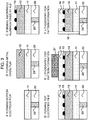
- FIG. 3 illustrates manufacturing steps of the resistive random access memory.
- the lower electrode 11 is formed on the contact plug 23 that has been formed in the interlayer insulating film 22.
- the lower electrode 11 is formed by stacking an adhesion layer and a conductive layer.
- the adhesion layer is made of Ti or chromium (Cr).
- the conductive layer can be made of a material ordinarily known in the art.
- Examples of the material for forming the conductive layer include metal materials, such as aluminum (Al), Pt, gold (Au), silver (Ag), Cu, nickel (Ni), molybdenum (Mo), Ta, tungsten (W), or alloys of these metal materials, or conductive oxides, such as indium tin oxide (ITO) or zinc oxide (ZnO).
- the conductive layer may be formed by stacking two or more layers, for example, by plating the surface of the conductive layer with a metal material.
- the metal oxide film 12 is formed as illustrated in B of FIG. 3 .
- the metal oxide film 12 is made of a material in which at least an element included in the metal oxide film has free energy for formation of oxides larger than free energy for formation of oxides of Al 2 O 3 , at least in a partial range of a temperature range from 0°C to 400°C (see TABLE 1).
- the forming is carried out in a temperature range that satisfies the magnitude relationship mentioned above, that is, [free energy for generating metal oxide (at least an element in the metal oxide film 12)] > [free energy for generating metal oxide (Al 2 O 3 )] (or in the temperature range in which oxygen vacancy is generated on the metal oxide film 12).
- the metal oxide film 12 may be made of a material that includes at least an element selected from the group consisting of Ti, Ta, Nb, Zr, and Hf. Such a metal oxide film 12 exhibits an excellent insulating characteristic in some manufacturing conditions, so that oxygen vacancy cannot easily be formed in the metal oxide film 12. Therefore, a high forming voltage needs to be applied to establish forming by the oxygen vacancy. In addition, forming is established randomly at various locations with large variations among memories.
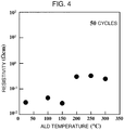
- FIG. 4 illustrates changes in resistivity of TiO 2 film, which is in the rutile structure, relative to ALD deposition temperature.
- the number of ALD cycles is fixed to 50 cycles.
- the resistivity is determined by a Hall measurement.
- the resistivity value decreases in the order from 10 -2 to 10 -1 ⁇ cm over the entire temperature range. This represents the change of TiO 2 from the insulator to the conductor.
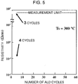
- FIG. 5 illustrates changes in resistivity of the TiO 2 film relative to the number of ALD cycles with the ALD deposition temperature fixed at 300°C.
- the resistivity value exhibits a measurement-limit insulating characteristic, but at four ALD cycles, the resistivity value sharply drops to 10 -1 ⁇ cm, representing conversion to the conductor.
- the resistivity value is in the order of 10 -2 to 10 -1 ⁇ cm after three cycles, representing that the TiO 2 film remains as the conductor.
- the ALD controls a film thickness of Al 2 O 3 film by changing the number of cycles for alternately supplying the TMA precursor, and the H 2 O gas.
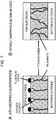
- the film forming speed is from 0.08 to 0.15 nm/cycle, and the formation is in the island-shaped and particulate formation and in a distributed manner up to three cycles, as illustrated in A of FIG. 6 , but changes to a film after three cycles, as illustrated in B of FIG. 6 .
- Electrons do not flow up to three cycles due to a distance between adjacent oxygen vacancy locations. After three cycles, electrons begin to flow because the distance between the oxygen vacancy locations approaches to a range in which electrons can flow.
- Formula 1 resembles oxygen movement caused by a difference in free energy for formation of oxides when two kinds of metal oxides come to touch each other.
- the free energy for formation of oxides of Al 2 O 3 for example, at 22°C is - 1060 kJ/mol, which is smaller than that of TiO 2 in the rutile structure, -888 kJ/mol, facilitating oxygen vacancy of TiO 2 .
- TABLE 1 that lists the free energy of metal oxides for oxide generation, a similar phenomenon as in the case of TiO 2 film occurs in terms of oxygen vacancy when the film of hafnium oxide (HfO 2 ), zirconium oxide (ZrO 2 ), niobium oxide (NbO), or tantalum oxide (Ta 2 O 5 ) is formed by ALD.
- HfO 2 hafnium oxide
- ZrO 2 zirconium oxide
- NbO niobium oxide
- Ta 2 O 5 tantalum oxide
- amorphous Al 2 O 3 is formed by ALD. It is generally known to persons in the art that thermal treatment at 900°C or more is required for crystallization. In particular, low defect and high quality Al 2 O 3 can preferably be formed in a stable manner in a film forming temperature range from 22°C to 300°C by ALD. If this condition is not satisfied, aluminum oxide including an impurity would be formed. Even when the H 2 O gas supply is insufficient or not present, amorphous aluminum oxycarbide is formed similarly in the island-shaped or particulate formation up to three cycles.
- the amorphous aluminum oxide or aluminum oxycarbide has an average particle size from 0.1 nm to 0.6 nm. If roughness becomes too large, insufficient contact with the upper electrode would occur.
- the oxide film 12 sandwiched between the lower electrode 11 and the upper electrode 14 should be an insulator, so that the metal oxide film that has turned to a conductor cannot be used.
- the metal oxide film maintains its insulating characteristic although oxygen vacancy is present under the deposition.
- a resistive random access memory capable of using the oxygen vacancy formed under the above-described aluminum oxide or aluminum oxycarbide as nuclei for growing filaments for the forming can be implemented. This is an underlying idea of the inventors to allow them to conceive the present invention.
- the island-shaped or particulate aluminum oxide 13 is formed by up to three cycles of ALD on the metal oxide film 12, as illustrated in C of FIG. 3 .
- the upper electrode 14 is formed as illustrated in FIG. 3D .
- the upper electrode 14 can be made of a material ordinarily known in the art. Examples of materials for forming such an electrode include a metal material, such as Al, Pt, Au, Ag, Cu, Ni, Mo, Ta, W, or alloys of these metal materials, or a conductive oxide, such as ITO or ZnO. These electrodes may be formed by stacking two or more layers, for example, by plating the surface of the electrodes with a metal material.
- a resist pattern 27 in a size of a memory is formed by an ordinary photolithography process. After etching down to the lower electrode 11 by an etching process, the resist film is peeled off to complete a resistive random access memory, as illustrated in F of FIG. 3 .
- FIG. 7 is a schematic cross-sectional view illustrating formation of filaments by oxygen vacancy when amorphous aluminum oxide is present (A) and not present (B).
- A amorphous aluminum oxide
- B a large forming voltage is applied to introduce oxygen vacancy.
- the oxygen vacancy occurs randomly and the filaments are formed from such oxygen vacancy.
- the forming voltage is high in the structure of B because a high voltage is necessary for forming oxygen vacancy that serves as nuclei of the filaments on the surface of the oxide layer in the initial step of forming.
- the voltage necessary for forming the oxygen vacancy changes according to the film quality of the surface, that is, only a small difference in manufacturing conditions. Thus, large variations occur among chips.
- the oxygen vacancy is formed on the surface of the TiO 2 film facing the aluminum oxide in a distributed manner. It has been found, therefore, a low forming voltage is necessary and a variation among memories is small.
- the oxygen vacancy already exists when aluminum oxide is formed on the surface of the oxide layer.
- a high forming voltage is not necessary in the initial step of the forming on the contrary to the conventional structure.
- the variation decreases because the influence of the forming voltage on the film quality is eliminated.
- the ALD has been described as a method for forming the island-shaped or particulate aluminum oxide or aluminum oxycarbide, but the method is not limited to ALD. Any method can be adopted so long as the method can control the formation of the island-shaped or particulate regions of aluminum oxide or aluminum oxycarbide in such a manner to cease the growth process before such regions extend laterally and connect with each other to form a continuous film.
- a MOCVD method used with a supply of TMA gas can be used for growth control.
- the structure similar to the resistive random access memory 10 illustrated in FIG. 1 was formed on silicon oxide (SiO) (100nm).
- the resistive random access memory of the present example was made with an Si substrate by forming an SiO 2 layer having a thickness of 100 nm by surface oxidization of an Si substrate, followed by forming a Ti film, as an adhesion layer, having a film thickness of 10 nm by DC sputtering at room temperature with Ar gas at 0.1 Pa and sputtering power of 200 W.
- the lower electrode 11 was formed by forming a Pt film having a film thickness of 100 nm as a conductive film on the Ti film by DC sputtering at room temperature with Ar gas at 0.1 Pa and sputtering power of 200 W.
- a TiO 2 film having a thickness of about 10 nm was formed as the metal oxide film 12 on the Pt film by an ALD apparatus at a temperature in a TDMAT raw material container of 100°C, a temperature of an H 2 O container of 20°C, a degree of vacuum at 10 Pa, and a growth temperature of 300°C in 200 cycles.
- Each cycle consists of a supply sequence of raw material: tetrakis-dimethlamido-titanium (TDMAT) ⁇ Ar purge gas H 2 O oxide gas ⁇ Ar purge gas.
- the TiO 2 film was in the amorphous structure. Such amorphous films were treated with heat at 500°C in an oxygen atmosphere and at 800°C in a nitrogen atmosphere, respectively, to form anatase and rutile structures. An example of the TiO 2 film in the rutile structure is described below.
- the amorphous aluminum oxide 13 was formed on the TiO 2 film in the rutile structure by an ALD apparatus at a temperature in TMA raw material container from 0°C to 20°C, a temperature of H 2 O container from 0°C to 20°C, a degree of vacuum at 10 Pa, and a growth temperature from 0°C to 400°C in 1 to 100 cycles.
- Each cycle consists of a supply sequence of raw material, TMA ⁇ Ar purge gas ⁇ H 2 O oxide gas ⁇ Ar purge gas.
- An example described below was made at a film forming temperature of 300°C in three cycles.
- the upper electrode 14 having a film thickness of 100 nm was made by depositing a Pt film through a stencil mask that includes pores each having a diameter of 100 ⁇ m by DC sputtering at room temperature, at Ar gas of 0.1 Pa, and sputtering power of 200 W.
- FIGS. 8 and 9 are graphs illustrating results of measurement of the characteristics of the resistive random access memory 10, in which FIG. 8 illustrates a variation characteristic of forming voltage between different elements and FIG. 9 illustrates a reliability characteristic.
- FIG. 8 is a bar graph illustrating the variation characteristic in forming voltage among elements. Bars with relatively small checkerboard pattern represent measurement results of the resistive random access memory 10 of the present example, while bars with distributed pattern of small dots represent data of a comparative example in which no amorphous aluminum oxide is provided.
- the resistive random access memory that does not include the amorphous aluminum oxide exhibited a wide distribution range of the forming voltage from 1.8 to 4.5 V. To securely establish forming in the element, the forming voltage needed to be applied even in a high voltage region.
- the resistive random access memory that includes the amorphous aluminum oxide according to the present example exhibited that about 75% of the memories was concentrated at the forming voltage of 2.5 V and the distribution range of the forming voltage was much narrower than that of the comparative example data. Namely, the present example exhibited an effect of decreasing the variation of the forming voltage.
- FIG. 9 illustrates the reliability characteristic of the resistive random access memory that includes amorphous aluminum oxide after the forming relative to the number of voltage cycles.
- the result exhibited a gradual increase of low resistance values after the number of cycles exceeded 60 cycles, representing a trend that the ratio of high resistance value to low resistance value decreased to below the five-order values. In some cases, breaking a capacitor in which the high resistance value was equal to the low resistance value was recognized.
- the present invention can largely contribute to improvement of the performance of the variable resistance device which is typically represented by the resistive random access memory.
Landscapes
- Chemical & Material Sciences (AREA)
- Engineering & Computer Science (AREA)
- Mechanical Engineering (AREA)
- Chemical Kinetics & Catalysis (AREA)
- General Chemical & Material Sciences (AREA)
- Materials Engineering (AREA)
- Inorganic Chemistry (AREA)
- Metallurgy (AREA)
- Organic Chemistry (AREA)
- Manufacturing & Machinery (AREA)
- Semiconductor Memories (AREA)
- Chemical Vapour Deposition (AREA)
- Formation Of Insulating Films (AREA)
Abstract
Description
- This application claims priority to Japanese Patent Application No.
2015-005464 filed on January 15, 2015 - The present invention relates to a variable resistance device that can be used as a non-volatile memory or the like, and a method for manufacturing the same.
- One example of typical non-volatile memories is a resistive random access memory (ReRAM) that uses resistance change caused by voltage application to insulating films provided between top and bottom electrodes. Researches and developments have been conducted vigorously to achieve high performance, highly reliable, and low cost ReRAMs.
- ReRAMs are formed in a simple metal-insulator-metal (MIM) structure and have a low process temperature, making ReRAMs be compatible with complementary metal-oxide-semiconductor (CMOS) logic. Two main ways of memory operations of ReRAMs have been proposed as follows. One is a mechanism for forming conductive paths (filaments) extending between top and bottom electrodes by applying a voltage to diffuse an electrode material into an insulating film. Copper (Cu) and platinum (Pt) have been examined as typical electrode materials. The other is a mechanism for forming filaments between top and bottom electrodes by introducing oxygen vacancy into the insulating film by reduction reaction, using an ionic metal oxide as the insulating film. As a typical ionic metal oxide, nickel oxide (NiO), hafnium oxide (HfO2), titanium oxide (TiO2), and tantalum oxide (TaOx) have been examined. Memory operation is carried out using a low resistance state in which filaments are connected and a high resistance state in which filaments are disconnected in accordance with changes of the direction of voltage application (see, e.g., NON-PATENT
LITERATURE 1, 2). - ReRAMs require initial operation called forming, which is regarded as soft breakdown, to form the filaments. To decrease a high forming voltage as a result of random forming of the filaments, it has been disclosed that a polycrystalline oxide layer, which acts as an insulating film, and an amorphous layer thicker than the polycrystalline oxide layer are stacked to use filaments generated in the boundaries of the polycrystalline oxide layer (see, e.g., PATENT LITERATURE 1). An oxygen drawing substance is distributed at an interface between the electrode and the insulating film to introduce oxygen vacancy into the insulating layer (see, e.g., PATENT LITERATURE 2).
- However, in the formation of the filaments generating from the boundaries between polycrystalline oxide layers disclosed in the above PATENT LITERATURE, the number and physical property of the boundaries are largely affected by the fabrication conditions of the polycrystalline layers, causing variations in the forming voltage. Meanwhile, the oxygen depleting substance to be distributed should be an oxide with oxygen vacancy, as represented by TiOx. It is difficult to regulate the amount of oxygen vacancy that determines the oxygen drawing amount from the insulating film. This makes it difficult to control the formation of filaments.
- In one report, the oxygen vacancy is introduced by removing oxygen from the top surface of single crystal SrTiO3. Oxygen of O-Ti bonds on the top surface of SrTiO3 is reacted with trimethylaluminium (TMA), Al(CH3)3, which is a raw material for film forming of an aluminum oxide (Al2O3) film by atomic layer deposition (ALD). As a result, a two-dimensional electron gas is generated (see, e.g., NON-PATENT LITERATURE 3). However, the removal of oxygen from the top surface suggested by the above NON-PATENT LITERATURE is limited to O-Ti bonds ordered on the single crystal substrate. A reaction between TMA and oxygen of O-Ti bonds in titanium oxide (TiO2) formed by amorphous body or polycrystal and the corresponding introduction of oxygen vacancy have not been suggested.
- In another report, natural oxide films can be removed by reacting oxygen of a natural oxide generated on a GaAs substrate (e.g., GaOx, AsOx) and TMA in the process of generating an aluminum oxide (Al2O3) film by ALD with TMA being as a raw material (see, e.g., NON-PATENT LITERATURE 4). However, the natural oxide disclosed in the above NON-PATENT LITERATURE is an oxygen-poor oxide, according to its stoichiometric ratio, in which oxygen easily reacts with TMA and no suggestion has been made about introducing oxygen vacancy by the reaction of oxygen in an oxygen-rich oxide having at least a stoichiometric composition ratio.
-
- PATENT LITERATURE 1: Japanese Patent No.
5309615 - PATENT LITERATURE 2:
JP 2014-22660 A -
- NON-PATENT LITERATURE 1: B. J. Choi et al., "Resistive switching mechanism of TiO2 thin films grown by atomic-layer deposition", J. Appl. Phys. Vol.98, 033715 (2005).
- NON-PATENT LITERATURE 2: S. Seo et al., "Reproducible resistance switching in polycrystalline NiO films", Appl. Phys. Lett., Vol.85, 5655 (2004).
- NON-PATENT LITERATURE 3: S. W. Lee et al., Nano Lett., Vol.12, 4775 (2012).
- NON-PATENT LITERATURE 4: H. D. Lee et al., Appl. Phys. Lett., Vol.94, 222108 (2009).
- The present invention has been made in view of the above situation and it is an object of the present invention to provide a variable resistance device, such as a ReRAM, having a uniform distribution of an amount of oxygen vacancy, and a method for manufacturing such a variable resistance device.
- According to an aspect of the present invention, a variable resistance device includes a film of metal oxide disposed between first and second electrodes, with island-shaped or particulate objects of amorphous aluminum oxide or aluminum oxycarbide being distributed between the first electrode and the metal oxide film.
- The average particle size of the island-shaped or particulate objects may be from 0.1 nm to 0.6 nm.
- At least an element included in the metal oxide may have free energy for formation of oxides larger than free energy for formation of oxides of aluminum oxide at least in a partial range of a temperature range from 0°C to 400°C.
- The metal oxide may include at least an element selected from the group consisting of titanium (Ti), tantalum (Ta), niobium (Nb), zirconium (Zr), and hafnium (Hf).
- According to another aspect of the present invention, a method for manufacturing a variable resistance device includes forming the island-shaped or particle-shaped objects made of aluminum oxide or aluminum oxycarbide on the metal oxide by ceasing the deposition before the deposition of the aluminum oxide or aluminum oxycarbide regions continues and the aluminum oxide or aluminum oxycarbide formed isolated from each other on the metal oxide at the early stage of deposition extends laterally and connect with each other to form a continuous film.
- The deposition may be carried out by atomic layer deposition (ALD).
- The number of ALD cycles carried out in the deposition by the ALD may be equal to or smaller than three cycles.
- The deposition by the ALD may use trimethylaluminum.
- The deposition by the ALD may be carried out in a temperature range from 0°C to 400°C.
- The deposition by the ALD may be carried out in a temperature range from 22°C to 300°C.
- The present invention can provide a variable resistance device, such as a ReRAM, having a low and stable forming voltage and an excellent resistance change characteristic.
-
- [
FIG.1] FIG. 1 is a schematic cross-sectional view of a variable resistance device according to an embodiment of the present invention. - [
FIG.2] FIG. 2 is a schematic cross-sectional view of a variable resistance device of type 1T-1R according to the embodiment of the present invention. - [
FIG.3] FIG. 3 illustrates manufacturing steps of the variable resistance device according to the embodiment of the present invention. - [
FIG.4] FIG. 4 illustrates results of changes in resistivity of TiO2 film relative to film forming temperatures of ALD according to the embodiment of the present invention. - [
FIG.5] FIG. 5 illustrates results of changes in resistivity of the TiO2 film relative to the number of ALD cycles according to the embodiment of the present invention. - [
FIG.6] FIG. 6 is a schematic diagram for explaining a difference in mechanism for oxygen vacancy and electron generation between three cycles or less and four cycles or more of ALD according to the embodiment of the present invention. - [
FIG.7] FIG. 7 is schematic diagrams of forming filaments with amorphous aluminum oxide according to the embodiment of the present invention. - [
FIG.8] FIG. 8 illustrates a variation characteristic of forming voltage among elements according to the embodiment of the present invention. - [
FIG.9] FIG. 9 illustrates reliability of a resistive random access memory that does not include amorphous aluminum oxide relative to the number of voltage cycles according to the embodiment of the present invention. - A variable resistance device and a method for manufacturing a variable resistance device according to an embodiment of the present invention will be described below by referring to the accompanying drawings. For convenience of viewing, sizes and ratios of constituent components are changed appropriately in the drawings. The following description mainly relates to a resistive random access memory, as it is a representative use of the variable resistance device, but as a matter of course, the variable resistance device can be applied to other uses without losing generality.
-
FIG. 1 is a schematic cross-sectional view of a resistiverandom access memory 10 according to an embodiment of the present invention. The resistiverandom access memory 10 includes ametal oxide film 12 provided between anupper electrode 14 and alower electrode 11. Amorphous aluminum oxide oraluminum oxycarbide 13 is distributed in an island-shaped or particle-shaped formation having an average particle size from 0.1 nm to 0.6 nm between theupper electrode 14 and themetal oxide film 12. -
FIG. 2 is a schematic cross-sectional view of a resistiverandom access memory 10 of type 1T-1R according to the embodiment of the present invention. Atransistor 17 is formed on asilicon substrate 15 that is divided byelectrical isolation 16. Thetransistor 17 includes a source (S) and a drain (D) formed by a generally COMS process. Aground line 20 is formed on acontact plug 19 formed in aninterlayer insulating film 18 on the source (S). Aninterconnect line 21 is formed on anothercontact plug 19 formed in theinterlayer insulating film 18 on the drain (D). Acontact plug 23 is formed in aninterlayer insulating film 22 on theinterconnect line 21. Thelower electrode 11 of the resistiverandom access memory 10 is then formed on thecontact plug 23. Acontact plug 25 is formed penetrating through theupper electrode 14 of the resistiverandom access memory 10 having been formed as described above. Abit line 26 is formed on thecontact plug 25 through theinterlayer insulating film 24. -
FIG. 3 illustrates manufacturing steps of the resistive random access memory. In A ofFIG. 3 , thelower electrode 11 is formed on thecontact plug 23 that has been formed in theinterlayer insulating film 22. Thelower electrode 11 is formed by stacking an adhesion layer and a conductive layer. The adhesion layer is made of Ti or chromium (Cr). The conductive layer can be made of a material ordinarily known in the art. Examples of the material for forming the conductive layer include metal materials, such as aluminum (Al), Pt, gold (Au), silver (Ag), Cu, nickel (Ni), molybdenum (Mo), Ta, tungsten (W), or alloys of these metal materials, or conductive oxides, such as indium tin oxide (ITO) or zinc oxide (ZnO). The conductive layer may be formed by stacking two or more layers, for example, by plating the surface of the conductive layer with a metal material. - The
metal oxide film 12 is formed as illustrated in B ofFIG. 3 . Themetal oxide film 12 is made of a material in which at least an element included in the metal oxide film has free energy for formation of oxides larger than free energy for formation of oxides of Al2O3, at least in a partial range of a temperature range from 0°C to 400°C (see TABLE 1). Naturally, the forming is carried out in a temperature range that satisfies the magnitude relationship mentioned above, that is, [free energy for generating metal oxide (at least an element in the metal oxide film 12)] > [free energy for generating metal oxide (Al2O3)] (or in the temperature range in which oxygen vacancy is generated on the metal oxide film 12). - The
metal oxide film 12 may be made of a material that includes at least an element selected from the group consisting of Ti, Ta, Nb, Zr, and Hf. Such ametal oxide film 12 exhibits an excellent insulating characteristic in some manufacturing conditions, so that oxygen vacancy cannot easily be formed in themetal oxide film 12. Therefore, a high forming voltage needs to be applied to establish forming by the oxygen vacancy. In addition, forming is established randomly at various locations with large variations among memories. - The inventors of the present application have repeatedly examined to solve this problem to find that a TiO2 film changes from insulator to conductor at a relatively early stage of an aluminum oxide film deposition by ALD with TMA precursor and a H2O gas on a TiO2 film that is in rutile structure and has a film thickness of 10 nm formed on a glass substrate.
FIG. 4 illustrates changes in resistivity of TiO2 film, which is in the rutile structure, relative to ALD deposition temperature. The number of ALD cycles is fixed to 50 cycles. The resistivity is determined by a Hall measurement. The resistivity value decreases in the order from 10-2 to 10-1 Ω cm over the entire temperature range. This represents the change of TiO2 from the insulator to the conductor.FIG. 5 illustrates changes in resistivity of the TiO2 film relative to the number of ALD cycles with the ALD deposition temperature fixed at 300°C. Up to three ALD cycles, the resistivity value exhibits a measurement-limit insulating characteristic, but at four ALD cycles, the resistivity value sharply drops to 10-1 Ω cm, representing conversion to the conductor. The resistivity value is in the order of 10-2 to 10-1 Ω cm after three cycles, representing that the TiO2 film remains as the conductor. - A difference between three cycles and four cycles or more is described by referring to
FIG. 6 . The ALD controls a film thickness of Al2O3 film by changing the number of cycles for alternately supplying the TMA precursor, and the H2O gas. The film forming speed is from 0.08 to 0.15 nm/cycle, and the formation is in the island-shaped and particulate formation and in a distributed manner up to three cycles, as illustrated in A ofFIG. 6 , but changes to a film after three cycles, as illustrated in B ofFIG. 6 . Even in the island-shaped and particulate regions, electrons are generated by introducing oxygen vacancy to the TiO2 film. This is supposedly carried out in accordance with the following mechanism. When the raw material, TMA, adheres to the surface of the TiO2 film, oxygen on the top surface of the TiO2 film reacts with Al element and CH3 group of the raw material, TMA, to generate Al2O3 and CO2 gas. Along with the generation, oxygen vacancy occurs in the TiO2 film.Formula 1 represents this reaction. This reaction is also disclosed inNON-PATENT LITERATURE 3.
[Formula 1] 2Al(CH3)3+10TiO2 → Al2O3+5Ti2O3+3CH4(g)+C2H4(g)+CO2(g)+H2(g)
- Electrons do not flow up to three cycles due to a distance between adjacent oxygen vacancy locations. After three cycles, electrons begin to flow because the distance between the oxygen vacancy locations approaches to a range in which electrons can flow.
Formula 1 resembles oxygen movement caused by a difference in free energy for formation of oxides when two kinds of metal oxides come to touch each other. In a temperature range from 0°C to 400°C of ALD deposition, the free energy for formation of oxides of Al2O3, for example, at 22°C is - 1060 kJ/mol, which is smaller than that of TiO2 in the rutile structure, -888 kJ/mol, facilitating oxygen vacancy of TiO2. As illustrated in TABLE 1 that lists the free energy of metal oxides for oxide generation, a similar phenomenon as in the case of TiO2 film occurs in terms of oxygen vacancy when the film of hafnium oxide (HfO2), zirconium oxide (ZrO2), niobium oxide (NbO), or tantalum oxide (Ta2O5) is formed by ALD.[TABLE 1] OXIDE TEMPERATURE (°C) FREE ENERGY FOR GENERATING OXIDE (kJ/mol) Al2O3 0 -1065 22 -1060 300 -999 400 -977 HfO2 0 -1014 22 -1010 300 -962 400 -946 ZrO2 0 -975 22 -1039 300 -989 400 -971 TiO2 0 -892 (Rutile) 22 -888 300 -838 400 -820 NbO 0 -779 22 -775 300 -728 400 -670 Ta2O5 0 -764 22 -760 300 -713 400 -696 - In a temperature range from 0°C to 400°C, amorphous Al2O3 is formed by ALD. It is generally known to persons in the art that thermal treatment at 900°C or more is required for crystallization. In particular, low defect and high quality Al2O3 can preferably be formed in a stable manner in a film forming temperature range from 22°C to 300°C by ALD. If this condition is not satisfied, aluminum oxide including an impurity would be formed. Even when the H2O gas supply is insufficient or not present, amorphous aluminum oxycarbide is formed similarly in the island-shaped or particulate formation up to three cycles.
- Preferably, the amorphous aluminum oxide or aluminum oxycarbide has an average particle size from 0.1 nm to 0.6 nm. If roughness becomes too large, insufficient contact with the upper electrode would occur.
- According to the operation principle of the resistive random access memory, the
oxide film 12 sandwiched between thelower electrode 11 and theupper electrode 14 should be an insulator, so that the metal oxide film that has turned to a conductor cannot be used. However, as described above, at the early stage of deposition of aluminum oxide or aluminum oxycarbide, the metal oxide film maintains its insulating characteristic although oxygen vacancy is present under the deposition. By using this characteristic, a resistive random access memory capable of using the oxygen vacancy formed under the above-described aluminum oxide or aluminum oxycarbide as nuclei for growing filaments for the forming can be implemented. This is an underlying idea of the inventors to allow them to conceive the present invention. - To satisfy the above condition in accordance with such an idea, the island-shaped or
particulate aluminum oxide 13 is formed by up to three cycles of ALD on themetal oxide film 12, as illustrated in C ofFIG. 3 . Theupper electrode 14 is formed as illustrated inFIG. 3D . Theupper electrode 14 can be made of a material ordinarily known in the art. Examples of materials for forming such an electrode include a metal material, such as Al, Pt, Au, Ag, Cu, Ni, Mo, Ta, W, or alloys of these metal materials, or a conductive oxide, such as ITO or ZnO. These electrodes may be formed by stacking two or more layers, for example, by plating the surface of the electrodes with a metal material. - As illustrated in E of
FIG. 3 , a resistpattern 27 in a size of a memory is formed by an ordinary photolithography process. After etching down to thelower electrode 11 by an etching process, the resist film is peeled off to complete a resistive random access memory, as illustrated in F ofFIG. 3 . -
FIG. 7 is a schematic cross-sectional view illustrating formation of filaments by oxygen vacancy when amorphous aluminum oxide is present (A) and not present (B). In the case of B, a large forming voltage is applied to introduce oxygen vacancy. The oxygen vacancy occurs randomly and the filaments are formed from such oxygen vacancy. As a result, a large variation occurs among memories. Specifically, the forming voltage is high in the structure of B because a high voltage is necessary for forming oxygen vacancy that serves as nuclei of the filaments on the surface of the oxide layer in the initial step of forming. In addition, the voltage necessary for forming the oxygen vacancy changes according to the film quality of the surface, that is, only a small difference in manufacturing conditions. Thus, large variations occur among chips. On the other hand, in the case of A, the oxygen vacancy is formed on the surface of the TiO2 film facing the aluminum oxide in a distributed manner. It has been found, therefore, a low forming voltage is necessary and a variation among memories is small. In other words, in the structure of A, the oxygen vacancy already exists when aluminum oxide is formed on the surface of the oxide layer. A high forming voltage is not necessary in the initial step of the forming on the contrary to the conventional structure. In addition, the variation decreases because the influence of the forming voltage on the film quality is eliminated. - The ALD has been described as a method for forming the island-shaped or particulate aluminum oxide or aluminum oxycarbide, but the method is not limited to ALD. Any method can be adopted so long as the method can control the formation of the island-shaped or particulate regions of aluminum oxide or aluminum oxycarbide in such a manner to cease the growth process before such regions extend laterally and connect with each other to form a continuous film. For example, a MOCVD method used with a supply of TMA gas can be used for growth control.
- Examples of the present invention will be described below, but these examples do not limit the scope of the present invention in any way. It is, therefore, apparent to persons in the art that various changes and corrections are possible within the scope of the present invention and the range of the appended claims.
- In the example, the structure similar to the resistive
random access memory 10 illustrated inFIG. 1 was formed on silicon oxide (SiO) (100nm). - The resistive random access memory of the present example was made with an Si substrate by forming an SiO2 layer having a thickness of 100 nm by surface oxidization of an Si substrate, followed by forming a Ti film, as an adhesion layer, having a film thickness of 10 nm by DC sputtering at room temperature with Ar gas at 0.1 Pa and sputtering power of 200 W. The
lower electrode 11 was formed by forming a Pt film having a film thickness of 100 nm as a conductive film on the Ti film by DC sputtering at room temperature with Ar gas at 0.1 Pa and sputtering power of 200 W. - Subsequently, a TiO2 film having a thickness of about 10 nm was formed as the
metal oxide film 12 on the Pt film by an ALD apparatus at a temperature in a TDMAT raw material container of 100°C, a temperature of an H2O container of 20°C, a degree of vacuum at 10 Pa, and a growth temperature of 300°C in 200 cycles. Each cycle consists of a supply sequence of raw material: tetrakis-dimethlamido-titanium (TDMAT) → Ar purge gas H2O oxide gas → Ar purge gas. The TiO2 film was in the amorphous structure. Such amorphous films were treated with heat at 500°C in an oxygen atmosphere and at 800°C in a nitrogen atmosphere, respectively, to form anatase and rutile structures. An example of the TiO2 film in the rutile structure is described below. - Subsequently, the
amorphous aluminum oxide 13 was formed on the TiO2 film in the rutile structure by an ALD apparatus at a temperature in TMA raw material container from 0°C to 20°C, a temperature of H2O container from 0°C to 20°C, a degree of vacuum at 10 Pa, and a growth temperature from 0°C to 400°C in 1 to 100 cycles. Each cycle consists of a supply sequence of raw material, TMA → Ar purge gas → H2O oxide gas → Ar purge gas. An example described below was made at a film forming temperature of 300°C in three cycles. - Subsequently, the
upper electrode 14 having a film thickness of 100 nm was made by depositing a Pt film through a stencil mask that includes pores each having a diameter of 100 µm by DC sputtering at room temperature, at Ar gas of 0.1 Pa, and sputtering power of 200 W. - Thus, the resistive
random access memory 10 was manufactured and its characteristics were measured in an evaluation circumstance at a temperature of 25°C in a dark place in vacuum.FIGS. 8 and9 are graphs illustrating results of measurement of the characteristics of the resistiverandom access memory 10, in whichFIG. 8 illustrates a variation characteristic of forming voltage between different elements andFIG. 9 illustrates a reliability characteristic. -
FIG. 8 is a bar graph illustrating the variation characteristic in forming voltage among elements. Bars with relatively small checkerboard pattern represent measurement results of the resistiverandom access memory 10 of the present example, while bars with distributed pattern of small dots represent data of a comparative example in which no amorphous aluminum oxide is provided. The resistive random access memory that does not include the amorphous aluminum oxide exhibited a wide distribution range of the forming voltage from 1.8 to 4.5 V. To securely establish forming in the element, the forming voltage needed to be applied even in a high voltage region. On the other hand, the resistive random access memory that includes the amorphous aluminum oxide according to the present example exhibited that about 75% of the memories was concentrated at the forming voltage of 2.5 V and the distribution range of the forming voltage was much narrower than that of the comparative example data. Namely, the present example exhibited an effect of decreasing the variation of the forming voltage. -
FIG. 9 illustrates the reliability characteristic of the resistive random access memory that includes amorphous aluminum oxide after the forming relative to the number of voltage cycles. A rectangular-wave voltage having an absolute value of 0.3 V and inverted polarities for every 10 msec was applied for 100 cycles. From the beginning of the repetition test until the repetition of 100 cycles was finished, a resistance difference (ratio of high resistance to low resistance), which was the important characteristic of the resistance change memory, exhibited favorable results of five-order difference with the order of 1E + 3 in the low resistance region and the order of 1E + 8 in the high resistance region. The five-order results were maintained after 100 cycles, representing a high reliability. On the other hand, the same cycle test was executed for the conventional capacitor that does not include aluminum oxide illustrated inFIG. 8 . The result exhibited a gradual increase of low resistance values after the number of cycles exceeded 60 cycles, representing a trend that the ratio of high resistance value to low resistance value decreased to below the five-order values. In some cases, breaking a capacitor in which the high resistance value was equal to the low resistance value was recognized. - As a result, the operation of the resistive random access memory of the present invention was confirmed and the usefulness of the present invention was proved.
- As described above, the present invention can largely contribute to improvement of the performance of the variable resistance device which is typically represented by the resistive random access memory.
-
- 10
- Resistive random access memory
- 11
- Lower electrode
- 12
- Metal oxide film
- 13
- Amorphous aluminum oxide or aluminum oxycarbide
- 14
- Upper electrode
- 15
- Silicon substrate
- 16
- Electrical isolation
- 17
- Transistor
- 18, 22, 24
- Interlayer insulating film
- 19,23,25
- Contact plug
- 20
- Ground line
- 21
- Interconnect line
- 26
- Bit line
Claims (11)
- A variable resistance device, comprising:a film of metal oxide disposed between a first electrode and a second electrode,wherein island-shaped or particulate objects of amorphous aluminum oxide or aluminum oxycarbide are distributed between the first electrode and the metal oxide film.
- The variable resistance device according to claim 1, wherein
an average particle size of each of the island-shaped or particulate objects is from 0.1 nm to 0.6 nm. - The variable resistance device according to claim 1 or 2, wherein
an absolute value of free energy for formation of oxides of at least one element included in the metal oxide is smaller than an absolute value of free energy for formation of oxides of aluminum oxide in at least a partial range of a temperature range from 0°C to 400°C. - The variable resistance device according to any one of claims 1 to 3, wherein
the metal oxide includes at least one element selected from the group consisting of titanium (Ti), tantalum (Ta), niobium (Nb), zirconium (Zr), and hafnium (Hf). - A method for manufacturing a variable resistance device, comprising:forming a first electrode;forming a layer of metal oxide on the first electrode;forming island-shaped or particulate objects of amorphous aluminum oxide or aluminum oxycarbide on the layer of metal oxide, the island-shaped or particulate objects being formed by, before continued deposition causes mutually isolated regions formed at an early stage of the deposition to extend laterally during the deposition and merge into a form of a continuous film, ceasing the deposition; andforming a second electrode on the layer of metal oxide and the island-shaped or particulate objects.
- The method for manufacturing the variable resistance device according to claim 5, wherein the deposition is carried out by atomic layer deposition (ALD).
- The method for manufacturing the variable resistance device according to claim 6, wherein the number of ALD cycles carried out in the deposition by the ALD is equal to or smaller than three cycles.
- The method for manufacturing the variable resistance device according to claim 6 or 7, wherein the deposition by the ALD is carried out with trimethylaluminum.
- The method for manufacturing the variable resistance device according to claim 8, wherein the deposition by the ALD is carried out at a temperature from 0°C to 400°C.
- The method for manufacturing the variable resistance device according to claim 9, wherein the deposition by the ALD is carried out at a temperature from 22°C to 300°C.
- The method for manufacturing the variable resistance device according to any one of claims 5 to 10, wherein the metal oxide includes at least one element selected from the group consisting of titanium (Ti), tantalum (Ta), niobium (Nb), zirconium (Zr), and hafnium (Hf).
Applications Claiming Priority (2)
| Application Number | Priority Date | Filing Date | Title |
|---|---|---|---|
| JP2015005464A JP6544555B2 (en) | 2015-01-15 | 2015-01-15 | Method of manufacturing resistance variable element |
| PCT/JP2016/050853 WO2016114311A1 (en) | 2015-01-15 | 2016-01-13 | Resistance change element and method for manufacturing same |
Publications (3)
| Publication Number | Publication Date |
|---|---|
| EP3246947A1 true EP3246947A1 (en) | 2017-11-22 |
| EP3246947A4 EP3246947A4 (en) | 2018-10-31 |
| EP3246947B1 EP3246947B1 (en) | 2020-04-01 |
Family
ID=56405852
Family Applications (1)
| Application Number | Title | Priority Date | Filing Date |
|---|---|---|---|
| EP16737382.8A Not-in-force EP3246947B1 (en) | 2015-01-15 | 2016-01-13 | Resistance change element and method for manufacturing same |
Country Status (4)
| Country | Link |
|---|---|
| US (1) | US10290802B2 (en) |
| EP (1) | EP3246947B1 (en) |
| JP (1) | JP6544555B2 (en) |
| WO (1) | WO2016114311A1 (en) |
Cited By (2)
| Publication number | Priority date | Publication date | Assignee | Title |
|---|---|---|---|---|
| CN110676374A (en) * | 2019-05-22 | 2020-01-10 | 集美大学 | Resistive random access memory and preparation method thereof |
| US20240276895A1 (en) * | 2019-08-28 | 2024-08-15 | Tetramem Inc. | Rram crossbar array circuits with specialized interface layers for low current operation |
Families Citing this family (16)
| Publication number | Priority date | Publication date | Assignee | Title |
|---|---|---|---|---|
| RU2653399C2 (en) * | 2016-09-15 | 2018-05-08 | Федеральное государственное бюджетное учреждение науки Институт электрофизики Уральского отделения Российской академии наук (ИЭФ УрО РАН) | Method of amorphous oxide of aluminum coating by reactive evaporation of aluminum in low pressure discharge |
| CN107610733B (en) * | 2017-08-31 | 2020-05-19 | 华中科技大学 | Electric forming method for reducing forming voltage of resistive random access memory |
| CN110317061B (en) * | 2018-03-28 | 2021-06-15 | 山东理工大学 | A kind of method for preparing Al4O4C nanofibers |
| JP2020043240A (en) | 2018-09-11 | 2020-03-19 | キオクシア株式会社 | Memory device |
| CN109461812B (en) * | 2018-09-27 | 2022-07-29 | 西交利物浦大学 | Aluminum oxide-based RRAM and preparation method thereof |
| US12382847B2 (en) | 2020-07-06 | 2025-08-05 | Tetramem Inc. | Resistive random-access memory devices with multi-component electrodes and discontinuous interface layers |
| US12302768B2 (en) | 2021-05-12 | 2025-05-13 | Tetramem Inc. | Resistive random-access memory devices with multi-component electrodes |
| US11527712B2 (en) * | 2020-07-06 | 2022-12-13 | Tetramem Inc. | Low current RRAM-based crossbar array circuits implemented with interface engineering technologies |
| US12396375B2 (en) * | 2020-07-06 | 2025-08-19 | Tetramem Inc. | Resistive random-access memory devices with engineered electronic defects and methods for making the same |
| US12213390B2 (en) | 2021-05-12 | 2025-01-28 | Tetramem Inc. | Resistive random-access memory devices with multi-component electrodes |
| TWI824516B (en) * | 2021-05-12 | 2023-12-01 | 美商特憶智能科技公司 | Resistive random-access memory devices with multicomponent electrodes and discontinuous interface layers |
| US12543514B2 (en) | 2021-05-12 | 2026-02-03 | Tetramem Inc. | Resistive random-access memory devices with metal-nitride compound electrodes |
| US20230413697A1 (en) * | 2022-06-17 | 2023-12-21 | Tetramem Inc. | Resistive random-access memory devices with compound non-reactive electrodes |
| US20250143194A1 (en) * | 2023-11-01 | 2025-05-01 | Tetramem Inc. | Resistive random-access memory (rram) devices with doped switching oxides |
| WO2026127208A1 (en) * | 2024-12-10 | 2026-06-18 | 한국과학기술연구원 | Resistive memory device based on difference in ion mobility and method for manufacturing same |
| CN119522036B (en) * | 2025-01-20 | 2025-08-15 | 浙江大学 | Composite multilayer memristor and preparation method thereof |
Family Cites Families (21)
| Publication number | Priority date | Publication date | Assignee | Title |
|---|---|---|---|---|
| JP2007243009A (en) * | 2006-03-10 | 2007-09-20 | Renesas Technology Corp | Semiconductor device and manufacturing method thereof |
| JP5286565B2 (en) * | 2007-06-15 | 2013-09-11 | 株式会社日立国際電気 | Semiconductor device manufacturing method, substrate processing method, and substrate processing apparatus |
| US8367560B2 (en) * | 2007-06-15 | 2013-02-05 | Hitachi Kokusai Electric Inc. | Semiconductor device manufacturing method |
| US7745807B2 (en) * | 2007-07-11 | 2010-06-29 | International Business Machines Corporation | Current constricting phase change memory element structure |
| JP5309615B2 (en) | 2008-03-05 | 2013-10-09 | 富士通株式会社 | Resistance change type memory and manufacturing method thereof |
| KR101491623B1 (en) * | 2008-09-24 | 2015-02-11 | 삼성디스플레이 주식회사 | Display device and driving method thereof |
| JP2012080094A (en) * | 2010-09-10 | 2012-04-19 | Elpida Memory Inc | Semiconductor memory device and method for manufacturing the same |
| JP5390715B2 (en) * | 2010-12-01 | 2014-01-15 | キヤノンアネルバ株式会社 | Nonvolatile memory element and manufacturing method thereof |
| US8920339B2 (en) * | 2011-04-19 | 2014-12-30 | Porex Corporation | Liquid sampling, storage, transfer and delivery device |
| TW201304561A (en) * | 2011-07-11 | 2013-01-16 | Hannstar Display Corp | Loudspeaker structure for flat display |
| US8866121B2 (en) * | 2011-07-29 | 2014-10-21 | Sandisk 3D Llc | Current-limiting layer and a current-reducing layer in a memory device |
| JP5874905B2 (en) * | 2011-10-18 | 2016-03-02 | 国立研究開発法人物質・材料研究機構 | Method of manufacturing an alumina resistance change memory element |
| KR101882850B1 (en) * | 2011-12-29 | 2018-07-30 | 에스케이하이닉스 주식회사 | Resistance variable memory device and method for fabricating the same |
| JP2013157469A (en) * | 2012-01-30 | 2013-08-15 | Sharp Corp | Variable resistive element, and nonvolatile semiconductor storage device |
| TWI469408B (en) * | 2012-05-07 | 2015-01-11 | Univ Feng Chia | Ultra-thin multi-layered phase-change memory devices |
| KR20130126325A (en) * | 2012-05-11 | 2013-11-20 | 에스케이하이닉스 주식회사 | Resistance variable memory device and method for fabricating the same |
| JP2014022660A (en) * | 2012-07-20 | 2014-02-03 | Sharp Corp | Variable resistance element, and nonvolatile semiconductor memory device provided with variable resistance element |
| JP2014053568A (en) * | 2012-09-10 | 2014-03-20 | Toshiba Corp | Ferroelectric memory and method of manufacturing the same |
| JP5680045B2 (en) * | 2012-11-14 | 2015-03-04 | 株式会社東芝 | Magnetoresistive element and magnetic memory |
| US9105646B2 (en) * | 2012-12-31 | 2015-08-11 | Intermolecular, Inc. | Methods for reproducible flash layer deposition |
| US9368722B2 (en) * | 2013-09-06 | 2016-06-14 | Taiwan Semiconductor Manufacturing Company Ltd. | Resistive random access memory and manufacturing method thereof |
-
2015
- 2015-01-15 JP JP2015005464A patent/JP6544555B2/en not_active Expired - Fee Related
-
2016
- 2016-01-13 US US15/536,150 patent/US10290802B2/en not_active Expired - Fee Related
- 2016-01-13 WO PCT/JP2016/050853 patent/WO2016114311A1/en not_active Ceased
- 2016-01-13 EP EP16737382.8A patent/EP3246947B1/en not_active Not-in-force
Cited By (3)
| Publication number | Priority date | Publication date | Assignee | Title |
|---|---|---|---|---|
| CN110676374A (en) * | 2019-05-22 | 2020-01-10 | 集美大学 | Resistive random access memory and preparation method thereof |
| US20240276895A1 (en) * | 2019-08-28 | 2024-08-15 | Tetramem Inc. | Rram crossbar array circuits with specialized interface layers for low current operation |
| US12484462B2 (en) * | 2019-08-28 | 2025-11-25 | Tetramem Inc. | Methods for fabricating RRAM crossbar array circuits with specialized interface layers for low current operation |
Also Published As
| Publication number | Publication date |
|---|---|
| JP6544555B2 (en) | 2019-07-17 |
| WO2016114311A1 (en) | 2016-07-21 |
| US10290802B2 (en) | 2019-05-14 |
| EP3246947A4 (en) | 2018-10-31 |
| EP3246947B1 (en) | 2020-04-01 |
| US20170346006A1 (en) | 2017-11-30 |
| JP2016131216A (en) | 2016-07-21 |
Similar Documents
| Publication | Publication Date | Title |
|---|---|---|
| EP3246947B1 (en) | Resistance change element and method for manufacturing same | |
| US11985911B2 (en) | Methods for fabricating resistive random-access memory stacks | |
| US8692223B2 (en) | Resistance variable memory device including nano particles and method for fabricating the same | |
| TWI553923B (en) | Memristor based on mixed-metal-valent compound, preparation method and operation method thereof | |
| KR101988147B1 (en) | Structures incorporating and methods of forming metal lines including carbon | |
| KR100913395B1 (en) | Memory devices and method for fabricating the same | |
| AU2016361453B2 (en) | A memristor device and a method of fabrication thereof | |
| US20100258778A1 (en) | Resistive memory device and method for manufacturing the same | |
| US8350244B2 (en) | Variable resistance device, method for manufacturing variable resistance device, and semiconductor storage device using variable resistance device | |
| US9281477B2 (en) | Resistance change element and method for producing the same | |
| TW201212122A (en) | A high-k dielectric material and methods of forming the high-k dielectric material | |
| US9831426B2 (en) | CBRAM device and manufacturing method thereof | |
| KR102275269B1 (en) | Memory device and fabricating method of thereof | |
| KR101815799B1 (en) | Variable-resistance element and method for producing same | |
| WO2020139141A9 (en) | Method of manufacturing a memristor having an electric field nano-concentrator | |
| KR20130014004A (en) | Resistance variable memory device and method for fabricating the same | |
| Hoffmann-Eifert et al. | ALD Grown Functional Oxide Layers for Nonvolatile Resistive Switching Memory Applications |
Legal Events
| Date | Code | Title | Description |
|---|---|---|---|
| STAA | Information on the status of an ep patent application or granted ep patent |
Free format text: STATUS: THE INTERNATIONAL PUBLICATION HAS BEEN MADE |
|
| PUAI | Public reference made under article 153(3) epc to a published international application that has entered the european phase |
Free format text: ORIGINAL CODE: 0009012 |
|
| STAA | Information on the status of an ep patent application or granted ep patent |
Free format text: STATUS: REQUEST FOR EXAMINATION WAS MADE |
|
| 17P | Request for examination filed |
Effective date: 20170613 |
|
| AK | Designated contracting states |
Kind code of ref document: A1 Designated state(s): AL AT BE BG CH CY CZ DE DK EE ES FI FR GB GR HR HU IE IS IT LI LT LU LV MC MK MT NL NO PL PT RO RS SE SI SK SM TR |
|
| AX | Request for extension of the european patent |
Extension state: BA ME |
|
| DAV | Request for validation of the european patent (deleted) | ||
| DAX | Request for extension of the european patent (deleted) | ||
| A4 | Supplementary search report drawn up and despatched |
Effective date: 20181004 |
|
| RIC1 | Information provided on ipc code assigned before grant |
Ipc: H01L 27/105 20060101AFI20180927BHEP Ipc: H01L 45/00 20060101ALI20180927BHEP Ipc: C23C 16/40 20060101ALI20180927BHEP Ipc: H01L 49/00 20060101ALI20180927BHEP Ipc: H01L 21/316 20060101ALI20180927BHEP |
|
| STAA | Information on the status of an ep patent application or granted ep patent |
Free format text: STATUS: EXAMINATION IS IN PROGRESS |
|
| 17Q | First examination report despatched |
Effective date: 20190515 |
|
| GRAP | Despatch of communication of intention to grant a patent |
Free format text: ORIGINAL CODE: EPIDOSNIGR1 |
|
| STAA | Information on the status of an ep patent application or granted ep patent |
Free format text: STATUS: GRANT OF PATENT IS INTENDED |
|
| INTG | Intention to grant announced |
Effective date: 20200107 |
|
| GRAS | Grant fee paid |
Free format text: ORIGINAL CODE: EPIDOSNIGR3 |
|
| GRAA | (expected) grant |
Free format text: ORIGINAL CODE: 0009210 |
|
| STAA | Information on the status of an ep patent application or granted ep patent |
Free format text: STATUS: THE PATENT HAS BEEN GRANTED |
|
| AK | Designated contracting states |
Kind code of ref document: B1 Designated state(s): AL AT BE BG CH CY CZ DE DK EE ES FI FR GB GR HR HU IE IS IT LI LT LU LV MC MK MT NL NO PL PT RO RS SE SI SK SM TR |
|
| REG | Reference to a national code |
Ref country code: GB Ref legal event code: FG4D |
|
| REG | Reference to a national code |
Ref country code: AT Ref legal event code: REF Ref document number: 1252479 Country of ref document: AT Kind code of ref document: T Effective date: 20200415 Ref country code: CH Ref legal event code: EP |
|
| REG | Reference to a national code |
Ref country code: DE Ref legal event code: R096 Ref document number: 602016033039 Country of ref document: DE |
|
| REG | Reference to a national code |
Ref country code: IE Ref legal event code: FG4D |
|
| PG25 | Lapsed in a contracting state [announced via postgrant information from national office to epo] |
Ref country code: BG Free format text: LAPSE BECAUSE OF FAILURE TO SUBMIT A TRANSLATION OF THE DESCRIPTION OR TO PAY THE FEE WITHIN THE PRESCRIBED TIME-LIMIT Effective date: 20200701 |
|
| REG | Reference to a national code |
Ref country code: NL Ref legal event code: MP Effective date: 20200401 |
|
| REG | Reference to a national code |
Ref country code: LT Ref legal event code: MG4D |
|
| PG25 | Lapsed in a contracting state [announced via postgrant information from national office to epo] |
Ref country code: SE Free format text: LAPSE BECAUSE OF FAILURE TO SUBMIT A TRANSLATION OF THE DESCRIPTION OR TO PAY THE FEE WITHIN THE PRESCRIBED TIME-LIMIT Effective date: 20200401 Ref country code: IS Free format text: LAPSE BECAUSE OF FAILURE TO SUBMIT A TRANSLATION OF THE DESCRIPTION OR TO PAY THE FEE WITHIN THE PRESCRIBED TIME-LIMIT Effective date: 20200801 Ref country code: CZ Free format text: LAPSE BECAUSE OF FAILURE TO SUBMIT A TRANSLATION OF THE DESCRIPTION OR TO PAY THE FEE WITHIN THE PRESCRIBED TIME-LIMIT Effective date: 20200401 Ref country code: NL Free format text: LAPSE BECAUSE OF FAILURE TO SUBMIT A TRANSLATION OF THE DESCRIPTION OR TO PAY THE FEE WITHIN THE PRESCRIBED TIME-LIMIT Effective date: 20200401 Ref country code: FI Free format text: LAPSE BECAUSE OF FAILURE TO SUBMIT A TRANSLATION OF THE DESCRIPTION OR TO PAY THE FEE WITHIN THE PRESCRIBED TIME-LIMIT Effective date: 20200401 Ref country code: PT Free format text: LAPSE BECAUSE OF FAILURE TO SUBMIT A TRANSLATION OF THE DESCRIPTION OR TO PAY THE FEE WITHIN THE PRESCRIBED TIME-LIMIT Effective date: 20200817 Ref country code: LT Free format text: LAPSE BECAUSE OF FAILURE TO SUBMIT A TRANSLATION OF THE DESCRIPTION OR TO PAY THE FEE WITHIN THE PRESCRIBED TIME-LIMIT Effective date: 20200401 Ref country code: NO Free format text: LAPSE BECAUSE OF FAILURE TO SUBMIT A TRANSLATION OF THE DESCRIPTION OR TO PAY THE FEE WITHIN THE PRESCRIBED TIME-LIMIT Effective date: 20200701 Ref country code: GR Free format text: LAPSE BECAUSE OF FAILURE TO SUBMIT A TRANSLATION OF THE DESCRIPTION OR TO PAY THE FEE WITHIN THE PRESCRIBED TIME-LIMIT Effective date: 20200702 |
|
| REG | Reference to a national code |
Ref country code: AT Ref legal event code: MK05 Ref document number: 1252479 Country of ref document: AT Kind code of ref document: T Effective date: 20200401 |
|
| PG25 | Lapsed in a contracting state [announced via postgrant information from national office to epo] |
Ref country code: HR Free format text: LAPSE BECAUSE OF FAILURE TO SUBMIT A TRANSLATION OF THE DESCRIPTION OR TO PAY THE FEE WITHIN THE PRESCRIBED TIME-LIMIT Effective date: 20200401 Ref country code: LV Free format text: LAPSE BECAUSE OF FAILURE TO SUBMIT A TRANSLATION OF THE DESCRIPTION OR TO PAY THE FEE WITHIN THE PRESCRIBED TIME-LIMIT Effective date: 20200401 Ref country code: RS Free format text: LAPSE BECAUSE OF FAILURE TO SUBMIT A TRANSLATION OF THE DESCRIPTION OR TO PAY THE FEE WITHIN THE PRESCRIBED TIME-LIMIT Effective date: 20200401 |
|
| PG25 | Lapsed in a contracting state [announced via postgrant information from national office to epo] |
Ref country code: AL Free format text: LAPSE BECAUSE OF FAILURE TO SUBMIT A TRANSLATION OF THE DESCRIPTION OR TO PAY THE FEE WITHIN THE PRESCRIBED TIME-LIMIT Effective date: 20200401 |
|
| REG | Reference to a national code |
Ref country code: DE Ref legal event code: R097 Ref document number: 602016033039 Country of ref document: DE |
|
| PG25 | Lapsed in a contracting state [announced via postgrant information from national office to epo] |
Ref country code: SM Free format text: LAPSE BECAUSE OF FAILURE TO SUBMIT A TRANSLATION OF THE DESCRIPTION OR TO PAY THE FEE WITHIN THE PRESCRIBED TIME-LIMIT Effective date: 20200401 Ref country code: EE Free format text: LAPSE BECAUSE OF FAILURE TO SUBMIT A TRANSLATION OF THE DESCRIPTION OR TO PAY THE FEE WITHIN THE PRESCRIBED TIME-LIMIT Effective date: 20200401 Ref country code: RO Free format text: LAPSE BECAUSE OF FAILURE TO SUBMIT A TRANSLATION OF THE DESCRIPTION OR TO PAY THE FEE WITHIN THE PRESCRIBED TIME-LIMIT Effective date: 20200401 Ref country code: IT Free format text: LAPSE BECAUSE OF FAILURE TO SUBMIT A TRANSLATION OF THE DESCRIPTION OR TO PAY THE FEE WITHIN THE PRESCRIBED TIME-LIMIT Effective date: 20200401 Ref country code: DK Free format text: LAPSE BECAUSE OF FAILURE TO SUBMIT A TRANSLATION OF THE DESCRIPTION OR TO PAY THE FEE WITHIN THE PRESCRIBED TIME-LIMIT Effective date: 20200401 Ref country code: AT Free format text: LAPSE BECAUSE OF FAILURE TO SUBMIT A TRANSLATION OF THE DESCRIPTION OR TO PAY THE FEE WITHIN THE PRESCRIBED TIME-LIMIT Effective date: 20200401 Ref country code: ES Free format text: LAPSE BECAUSE OF FAILURE TO SUBMIT A TRANSLATION OF THE DESCRIPTION OR TO PAY THE FEE WITHIN THE PRESCRIBED TIME-LIMIT Effective date: 20200401 |
|
| PLBE | No opposition filed within time limit |
Free format text: ORIGINAL CODE: 0009261 |
|
| STAA | Information on the status of an ep patent application or granted ep patent |
Free format text: STATUS: NO OPPOSITION FILED WITHIN TIME LIMIT |
|
| PG25 | Lapsed in a contracting state [announced via postgrant information from national office to epo] |
Ref country code: PL Free format text: LAPSE BECAUSE OF FAILURE TO SUBMIT A TRANSLATION OF THE DESCRIPTION OR TO PAY THE FEE WITHIN THE PRESCRIBED TIME-LIMIT Effective date: 20200401 Ref country code: SK Free format text: LAPSE BECAUSE OF FAILURE TO SUBMIT A TRANSLATION OF THE DESCRIPTION OR TO PAY THE FEE WITHIN THE PRESCRIBED TIME-LIMIT Effective date: 20200401 |
|
| 26N | No opposition filed |
Effective date: 20210112 |
|
| PG25 | Lapsed in a contracting state [announced via postgrant information from national office to epo] |
Ref country code: SI Free format text: LAPSE BECAUSE OF FAILURE TO SUBMIT A TRANSLATION OF THE DESCRIPTION OR TO PAY THE FEE WITHIN THE PRESCRIBED TIME-LIMIT Effective date: 20200401 |
|
| PG25 | Lapsed in a contracting state [announced via postgrant information from national office to epo] |
Ref country code: MC Free format text: LAPSE BECAUSE OF FAILURE TO SUBMIT A TRANSLATION OF THE DESCRIPTION OR TO PAY THE FEE WITHIN THE PRESCRIBED TIME-LIMIT Effective date: 20200401 |
|
| REG | Reference to a national code |
Ref country code: CH Ref legal event code: PL |
|
| GBPC | Gb: european patent ceased through non-payment of renewal fee |
Effective date: 20210113 |
|
| PG25 | Lapsed in a contracting state [announced via postgrant information from national office to epo] |
Ref country code: LU Free format text: LAPSE BECAUSE OF NON-PAYMENT OF DUE FEES Effective date: 20210113 |
|
| REG | Reference to a national code |
Ref country code: BE Ref legal event code: MM Effective date: 20210131 |
|
| PG25 | Lapsed in a contracting state [announced via postgrant information from national office to epo] |
Ref country code: CH Free format text: LAPSE BECAUSE OF NON-PAYMENT OF DUE FEES Effective date: 20210131 Ref country code: GB Free format text: LAPSE BECAUSE OF NON-PAYMENT OF DUE FEES Effective date: 20210113 Ref country code: LI Free format text: LAPSE BECAUSE OF NON-PAYMENT OF DUE FEES Effective date: 20210131 |
|
| PG25 | Lapsed in a contracting state [announced via postgrant information from national office to epo] |
Ref country code: IE Free format text: LAPSE BECAUSE OF NON-PAYMENT OF DUE FEES Effective date: 20210113 |
|
| PG25 | Lapsed in a contracting state [announced via postgrant information from national office to epo] |
Ref country code: BE Free format text: LAPSE BECAUSE OF NON-PAYMENT OF DUE FEES Effective date: 20210131 |
|
| PGFP | Annual fee paid to national office [announced via postgrant information from national office to epo] |
Ref country code: FR Payment date: 20221208 Year of fee payment: 8 |
|
| PG25 | Lapsed in a contracting state [announced via postgrant information from national office to epo] |
Ref country code: HU Free format text: LAPSE BECAUSE OF FAILURE TO SUBMIT A TRANSLATION OF THE DESCRIPTION OR TO PAY THE FEE WITHIN THE PRESCRIBED TIME-LIMIT; INVALID AB INITIO Effective date: 20160113 |
|
| PGFP | Annual fee paid to national office [announced via postgrant information from national office to epo] |
Ref country code: DE Payment date: 20221207 Year of fee payment: 8 |
|
| PG25 | Lapsed in a contracting state [announced via postgrant information from national office to epo] |
Ref country code: CY Free format text: LAPSE BECAUSE OF FAILURE TO SUBMIT A TRANSLATION OF THE DESCRIPTION OR TO PAY THE FEE WITHIN THE PRESCRIBED TIME-LIMIT Effective date: 20200401 |
|
| PG25 | Lapsed in a contracting state [announced via postgrant information from national office to epo] |
Ref country code: MK Free format text: LAPSE BECAUSE OF FAILURE TO SUBMIT A TRANSLATION OF THE DESCRIPTION OR TO PAY THE FEE WITHIN THE PRESCRIBED TIME-LIMIT Effective date: 20200401 |
|
| REG | Reference to a national code |
Ref country code: DE Ref legal event code: R119 Ref document number: 602016033039 Country of ref document: DE |
|
| PG25 | Lapsed in a contracting state [announced via postgrant information from national office to epo] |
Ref country code: MT Free format text: LAPSE BECAUSE OF FAILURE TO SUBMIT A TRANSLATION OF THE DESCRIPTION OR TO PAY THE FEE WITHIN THE PRESCRIBED TIME-LIMIT Effective date: 20200401 |
|
| PG25 | Lapsed in a contracting state [announced via postgrant information from national office to epo] |
Ref country code: DE Free format text: LAPSE BECAUSE OF NON-PAYMENT OF DUE FEES Effective date: 20240801 |
|
| PG25 | Lapsed in a contracting state [announced via postgrant information from national office to epo] |
Ref country code: FR Free format text: LAPSE BECAUSE OF NON-PAYMENT OF DUE FEES Effective date: 20240131 |
|
| PG25 | Lapsed in a contracting state [announced via postgrant information from national office to epo] |
Ref country code: FR Free format text: LAPSE BECAUSE OF NON-PAYMENT OF DUE FEES Effective date: 20240131 Ref country code: DE Free format text: LAPSE BECAUSE OF NON-PAYMENT OF DUE FEES Effective date: 20240801 |
|
| PG25 | Lapsed in a contracting state [announced via postgrant information from national office to epo] |
Ref country code: TR Free format text: LAPSE BECAUSE OF FAILURE TO SUBMIT A TRANSLATION OF THE DESCRIPTION OR TO PAY THE FEE WITHIN THE PRESCRIBED TIME-LIMIT Effective date: 20200401 |