EP3246944B1 - Schutz eines integrierten schaltkreises - Google Patents
Schutz eines integrierten schaltkreises Download PDFInfo
- Publication number
- EP3246944B1 EP3246944B1 EP16198652.6A EP16198652A EP3246944B1 EP 3246944 B1 EP3246944 B1 EP 3246944B1 EP 16198652 A EP16198652 A EP 16198652A EP 3246944 B1 EP3246944 B1 EP 3246944B1
- Authority
- EP
- European Patent Office
- Prior art keywords
- circuit
- counter
- flip
- laser
- flops
- Prior art date
- Legal status (The legal status is an assumption and is not a legal conclusion. Google has not performed a legal analysis and makes no representation as to the accuracy of the status listed.)
- Active
Links
Images


Classifications
-
- H—ELECTRICITY
- H03—ELECTRONIC CIRCUITRY
- H03K—PULSE TECHNIQUE
- H03K19/00—Logic circuits, i.e. having at least two inputs acting on one output; Inverting circuits
- H03K19/02—Logic circuits, i.e. having at least two inputs acting on one output; Inverting circuits using specified components
- H03K19/173—Logic circuits, i.e. having at least two inputs acting on one output; Inverting circuits using specified components using elementary logic circuits as components
- H03K19/177—Logic circuits, i.e. having at least two inputs acting on one output; Inverting circuits using specified components using elementary logic circuits as components arranged in matrix form
- H03K19/17748—Structural details of configuration resources
- H03K19/17768—Structural details of configuration resources for security
-
- G—PHYSICS
- G06—COMPUTING OR CALCULATING; COUNTING
- G06F—ELECTRIC DIGITAL DATA PROCESSING
- G06F21/00—Security arrangements for protecting computers, components thereof, programs or data against unauthorised activity
- G06F21/70—Protecting specific internal or peripheral components, in which the protection of a component leads to protection of the entire computer
- G06F21/71—Protecting specific internal or peripheral components, in which the protection of a component leads to protection of the entire computer to assure secure computing or processing of information
- G06F21/75—Protecting specific internal or peripheral components, in which the protection of a component leads to protection of the entire computer to assure secure computing or processing of information by inhibiting the analysis of circuitry or operation
-
- G—PHYSICS
- G06—COMPUTING OR CALCULATING; COUNTING
- G06F—ELECTRIC DIGITAL DATA PROCESSING
- G06F21/00—Security arrangements for protecting computers, components thereof, programs or data against unauthorised activity
- G06F21/70—Protecting specific internal or peripheral components, in which the protection of a component leads to protection of the entire computer
- G06F21/86—Secure or tamper-resistant housings
- G06F21/87—Secure or tamper-resistant housings by means of encapsulation, e.g. for integrated circuits
-
- G—PHYSICS
- G09—EDUCATION; CRYPTOGRAPHY; DISPLAY; ADVERTISING; SEALS
- G09C—CIPHERING OR DECIPHERING APPARATUS FOR CRYPTOGRAPHIC OR OTHER PURPOSES INVOLVING THE NEED FOR SECRECY
- G09C1/00—Apparatus or methods whereby a given sequence of signs, e.g. an intelligible text, is transformed into an unintelligible sequence of signs by transposing the signs or groups of signs or by replacing them by others according to a predetermined system
-
- H—ELECTRICITY
- H03—ELECTRONIC CIRCUITRY
- H03K—PULSE TECHNIQUE
- H03K19/00—Logic circuits, i.e. having at least two inputs acting on one output; Inverting circuits
- H03K19/003—Modifications for increasing the reliability for protection
- H03K19/0033—Radiation hardening
-
- H—ELECTRICITY
- H03—ELECTRONIC CIRCUITRY
- H03K—PULSE TECHNIQUE
- H03K19/00—Logic circuits, i.e. having at least two inputs acting on one output; Inverting circuits
- H03K19/02—Logic circuits, i.e. having at least two inputs acting on one output; Inverting circuits using specified components
- H03K19/173—Logic circuits, i.e. having at least two inputs acting on one output; Inverting circuits using specified components using elementary logic circuits as components
- H03K19/177—Logic circuits, i.e. having at least two inputs acting on one output; Inverting circuits using specified components using elementary logic circuits as components arranged in matrix form
- H03K19/17704—Logic circuits, i.e. having at least two inputs acting on one output; Inverting circuits using specified components using elementary logic circuits as components arranged in matrix form the logic functions being realised by the interconnection of rows and columns
-
- H—ELECTRICITY
- H04—ELECTRIC COMMUNICATION TECHNIQUE
- H04L—TRANSMISSION OF DIGITAL INFORMATION, e.g. TELEGRAPHIC COMMUNICATION
- H04L9/00—Cryptographic mechanisms or cryptographic arrangements for secret or secure communications; Network security protocols
- H04L9/002—Countermeasures against attacks on cryptographic mechanisms
- H04L9/004—Countermeasures against attacks on cryptographic mechanisms for fault attacks
-
- H—ELECTRICITY
- H10—SEMICONDUCTOR DEVICES; ELECTRIC SOLID-STATE DEVICES NOT OTHERWISE PROVIDED FOR
- H10W—GENERIC PACKAGES, INTERCONNECTIONS, CONNECTORS OR OTHER CONSTRUCTIONAL DETAILS OF DEVICES COVERED BY CLASS H10
- H10W42/00—Arrangements for protection of devices
- H10W42/40—Arrangements for protection of devices protecting against tampering, e.g. unauthorised inspection or reverse engineering
- H10W42/405—Arrangements for protection of devices protecting against tampering, e.g. unauthorised inspection or reverse engineering using active circuits
-
- H—ELECTRICITY
- H04—ELECTRIC COMMUNICATION TECHNIQUE
- H04L—TRANSMISSION OF DIGITAL INFORMATION, e.g. TELEGRAPHIC COMMUNICATION
- H04L2209/00—Additional information or applications relating to cryptographic mechanisms or cryptographic arrangements for secret or secure communication H04L9/00
- H04L2209/12—Details relating to cryptographic hardware or logic circuitry
Definitions
- the present description relates generally to electronic circuits and, more particularly, to the protection of an integrated circuit against fault injections by laser attack.
- electronic circuits handle so-called secret data, that is to say to which it is desired to reserve access to certain users or circuits.
- fault injection attacks consist in disturbing the operation of the circuit by intervening on one or more bits that it manipulates.
- a category of fault injection attacks that the present description is aimed more particularly at relates to laser attacks which consist in pointing a laser beam at logic elements of the circuit in order to switch the bits processed by these elements. Examining the effect of this attack on circuit behavior, whether by direct examination of the data provided by the circuit or by indirect examination by performing a hidden channel analysis can allow the attacker to unlock a secret.
- Laser attacks are generally attacks carried out from the rear face of the integrated circuit after a treatment consisting in eroding the substrate.
- detectors in the form of networks of conductors (wire mesh) or photocurrent or current detectors.
- Another category of detectors that the present description is more particularly aimed at consists in providing logic elements of the flip-flop type, the sole function of which is to detect a change of state representative of an accidental or deliberate disturbance.
- EP-A-1993057 describes a method and a circuit for detecting a state disturbance of a flip-flop of an electronic circuit.
- the document WO2008 / 084016 describes a method and a circuit for protecting information contained in an electronic circuit.
- the document US2007 / 182575 describes a detector for detecting external manipulation of an electrical circuit.
- the document WO03 / 102510 describes a circuit for protection against hacking in electronic devices.
- One embodiment overcomes all or part of the drawbacks of the usual techniques for protection against laser attacks.
- One embodiment proposes a solution which is particularly suitable for laser attacks focusing on particular regions of the circuit.
- One embodiment proposes a solution for detecting a laser attack before it occurs on a sensitive element from the point of view of the security of the data that it manipulates.
- one embodiment provides a device for protecting an integrated circuit according to claim 1.
- said state machine increments said counter in the presence of an event detected by a detection element, while the counter is in an initial value.
- said counter is reset at the end of the time delay.
- the detection elements are flip-flops.
- the logic gates are of the OR type.
- One embodiment provides for an integrated circuit comprising a protection device.
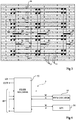
- the figure 1 is a schematic rear view of an integrated circuit 1 illustrating the state of the art and the problem posed.
- the representation of the figure 1 is very schematic and only partially represents the circuit.
- Circuit 1 is equipped with fault detectors 2 regularly distributed over its surface, at least in the sensitive areas from the point of view of the security of the data handled.
- Each detector 2 is typically a flip-flop, for example a D flip-flop whose state will be modified by the arrival of radiation from the rear face. All the flip-flops are connected to an analysis circuit which triggers a countermeasure, for example a reinitialization of the circuit, at the slightest disturbance detected.
- detectors of this type necessarily takes up space in circuit 1 and they are therefore distributed with an interval depending on the desired detection precision.
- the laser beams used had a beam diameter (spot) 32 such that the beam necessarily hit one of the detectors during an attack.
- spot 32
- laser attacks are now carried out with more focused beams and therefore with a significantly smaller impact diameter on the circuit. These new attacks make it possible to bypass certain countermeasures.
- a laser attack now generally begins with a scan of the rear face of circuit 1 in order to determine the positions of the detectors. Indeed, thanks to the fineness of the beam 34, by scanning the circuit, we will alternate the times when the circuit reacts, that is to say that we have touched a detector, and the times when the circuit does not react. not. This allows the attacker to map the detectors in order to then focus his attack on unprotected areas into which he can inject faults.
- the focusing of the laser beams becomes such that a detector is unable to distinguish a photon from a laser from an alpha particle from, for example, cosmic radiation.
- provision is made to integrate, in the circuit, networks or groups of radiation detectors in the form of networks or groups of flip-flops. Furthermore, provision is preferably made for a particular interpretation of the signals of these flip-flops taking into account a temporal aspect.
- the role of the detection device described is to detect a laser scan of the circuit which generally constitutes the step prior to a laser attack proper. Thus, the attack is detected before it is exploited on one of the sensitive components from the point of view of the security of the data handled.
- the figure 2 schematically and partially represents an embodiment of a laser attack detection architecture 4.
- each flip-flop 42 is, for example, a D flip-flop whose data input is grounded and whose direct output Q is connected to two inputs of two logic gates 44 and 46 of the OR type.
- Each logic gate 44 receives as input the signals from the flip-flops of a given row.
- Each logic gate 46 receives the signals from the flip-flops of a given column.
- each flip-flop 42 is connected to a gate 44 combining the signals from the flip-flops of the row and to a gate 46 combining the signals from the flip-flops of the column.
- the figure 3 schematically shows an integrated circuit equipped with an embodiment of a laser attack detection architecture as shown in figure 2 .
- FIG. 3 there is schematically and horizontally illustrated the alternating succession of P-type wells 12 and of N-type wells 14 in which the logic transistors are formed. This representation is very schematic and simply illustrates that the protection architecture is integrated into the logic zone of the integrated circuit.
- the figure 3 arbitrarily represent the case of a matrix network of three columns and four rows of groups of four flip-flops 42 each.
- the architecture, or detection device, shown therefore comprises six gates 46 (two per column) and eight gates 44 (two per row).
- the figure 4 represents, schematically and in the form of blocks, an embodiment of a circuit 5 for interpreting signals supplied by the architecture of the figures 2 and 3 .
- Circuit 5 comprises a state machine, preferably a state machine 52 (STATE MACHINE) in wired logic or a programmable logic network (FPGA), whose inputs IN are individually connected to the respective outputs of the gates 44 and 46 of protection architecture ( figure 3 ).
- Circuit 5 also includes a counter 54 (NVM COUNTER) in non-volatile memory and a delay line 56.
- the counter 54 is written W and read R by the state machine 52.
- the delay line is activated W and its state (active or expired delay) is read R by the state machine 52.
- Circuit 5 also includes an EN activation input which makes it possible, if necessary, to activate / deactivate the protection according to the phases of use of the device. , and an output OUT providing a signal indicative of a detected attack.
- circuit 5 more precisely of its state machine 52, is as follows.
- the state machine 52 increments the counter 54 and activates the delay line 56.
- the state machine determines whether the tilting comes from a rocker close to the previous one. If so, the counter 54 is incremented again and the delay line 56 is also activated again, i.e. the time constant is reset.
- the interpretation of the counter is made by the state machine 52 which periodically compares the state of the counter 54 with a threshold. As soon as the threshold is reached, the presence of an attack is considered and the state machine 52 switches the state of its output OUT.
- the choice of the distance from the neighborhood taken into account depends on the granularity of the groups of rockers in the circuit and on the expected speed of a laser scanning.
- the choice of the time constant of the delay line 56 also depends on the granularity of the groups of flip-flops in the circuit and on the expected speed of a laser scan.
- the triggering threshold of the alarm that is to say the threshold from which the output OUT switches depends on the applications. For example, we choose a threshold between 2 and 10.
- the reaction of the integrated circuit to a switching of the output OUT preferably consists in blocking the circuit and not in a simple restart. Indeed, if a scanning is detected, it is certain that the circuit will then be attacked by laser. with a targeted attack. It is therefore necessary to prevent any further operation. For example, we activate a fuse in non-volatile memory which permanently blocks the circuit.
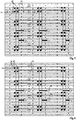
- the figures 5, 6 and 7 illustrate, by schematic views of an integrated circuit embodiment, its operation in the presence of different laser drive modes.
- the figure 5 illustrates the case of a sweep spaced by an interval greater than the interval between two flip-flops 42 of a group.
- the laser beam 34 will touch a first latch of a group but not the next latch of the same group.
- this beam during the scan will statistically inevitably affect a flip-flop of a following group, or even one of the logic gates 56 of the row. If the configuration of the state machine 52 is such that it takes the neighboring column into account, by arbitrarily assuming in this example a threshold of 2 for the counter, the sweep attack is detected.
- the figure 6 illustrates the case of continuous scanning, that is to say in which the laser spots touch each other.
- the triggering will take place from the first group of flip-flops 42 crossed by the sweep.
- the figure 7 illustrates the case of a skew sweep, that is, the case where the sweep is not parallel to the rows or columns of the matrix arrangement. Nevertheless, the laser spots 34 will statistically still reach several flip-flops 42 or gates 44 or 46. Therefore, the scanning is also detected here.
- each group of flip-flops comprises nine flip-flops in a 3x3 matrix arrangement rather than 4 flip-flops in a 2x2 matrix arrangement.
- the flip-flops 42 have been shown but not their connections, nor the rest of the architecture.
- An advantage of the embodiments described is that, unlike the usual systems, there is no reaction. immediate in the presence of a tilting of a detection element (a rocker). Thus, a hacker does not realize, while performing his scan, that he has hit a detector.
- One advantage of the embodiments described is that the risk of taking accidental radiation into account is very low. Indeed, such radiations will touch the circuit at random positions and, consequently, will not trigger the threshold.
Landscapes
- Engineering & Computer Science (AREA)
- Physics & Mathematics (AREA)
- Computer Hardware Design (AREA)
- Mathematical Physics (AREA)
- General Engineering & Computer Science (AREA)
- Computer Security & Cryptography (AREA)
- Theoretical Computer Science (AREA)
- Computing Systems (AREA)
- General Physics & Mathematics (AREA)
- Software Systems (AREA)
- Microelectronics & Electronic Packaging (AREA)
- Computer Networks & Wireless Communication (AREA)
- Signal Processing (AREA)
- Semiconductor Integrated Circuits (AREA)
- Design And Manufacture Of Integrated Circuits (AREA)
- Storage Device Security (AREA)
- Tests Of Electronic Circuits (AREA)
Claims (6)
- Schutzvorrichtung für eine integrierte Schaltung, die Folgendes aufweist:Gruppen von Strahlungsdetektionselementen (42), die in einer Matrixanordnung verteilt sind;Logikgatter (44, 46), die Ausgänge der Detektionselemente in Zeilen und in Spalten kombinieren, wobei jeder Ausgang eines Detektionselements mit einem Gatter verbunden ist, das eine Zeile kombiniert, und mit einem Gatter, das eine Spalte kombiniert; undeine Schaltung (5) zum Interpretieren von Signalen, die von den logischen Gattern geliefert werden, und die einen Ereigniszähler (54) von Ereignissen, die von einem der Detektionselemente erfasst werden, und ein Verzögerungselement (56) aufweist, wobei die Schaltung (5) eine Logikzustandsmaschine (52) umfasst, deren Eingänge (IN) einzeln mit den Ausgängen der Gatter (44, 46) verbunden sind,wobei die Vorrichtung so beschaffen ist, dass bei Vorhandensein eines von einem Detektionselement (42) erfassten Ereignisses die Zustandsmaschine (52) das Verzögerungselement (56) aktiviert und den Zähler (54) inkrementiert, wenn das Intervall zwischen dem Ort des aktuellen Ereignisses und eines vorhergehenden Ereignisses kürzer als eine vorgegebene Distanz ist.
- Vorrichtung nach Anspruch 1, wobei die Zustandsmaschine (52) bei Vorliegen eines von einem Detektionselement (42) erfassten Ereignisses den sich auf einem Anfangswert befindlichen Zähler (54) inkrementiert.
- Vorrichtung nach einem der Ansprüche 1 und 2, wobei der Zähler (54) am Ende der Verzögerung (56) zurückgesetzt wird.
- Vorrichtung nach einem der Ansprüche 1 bis 3, wobei die Erfassungselemente Flip-Flops (42) sind.
- Vorrichtung nach einem der Ansprüche 1 bis 4, wobei die Logikgatter (44, 46) vom ODER-Typ sind.
- Integrierte Schaltung mit der Schutzvorrichtung nach einem der Ansprüche 1 bis 5.
Applications Claiming Priority (1)
| Application Number | Priority Date | Filing Date | Title |
|---|---|---|---|
| FR1654371A FR3051599A1 (fr) | 2016-05-17 | 2016-05-17 | Protection d'un circuit integre |
Publications (2)
| Publication Number | Publication Date |
|---|---|
| EP3246944A1 EP3246944A1 (de) | 2017-11-22 |
| EP3246944B1 true EP3246944B1 (de) | 2021-03-31 |
Family
ID=56990508
Family Applications (1)
| Application Number | Title | Priority Date | Filing Date |
|---|---|---|---|
| EP16198652.6A Active EP3246944B1 (de) | 2016-05-17 | 2016-11-14 | Schutz eines integrierten schaltkreises |
Country Status (4)
| Country | Link |
|---|---|
| US (2) | US9716502B1 (de) |
| EP (1) | EP3246944B1 (de) |
| CN (2) | CN206259946U (de) |
| FR (1) | FR3051599A1 (de) |
Families Citing this family (6)
| Publication number | Priority date | Publication date | Assignee | Title |
|---|---|---|---|---|
| FR3051599A1 (fr) * | 2016-05-17 | 2017-11-24 | Stmicroelectronics Rousset | Protection d'un circuit integre |
| FR3054344B1 (fr) * | 2016-07-25 | 2018-09-07 | Tiempo | Circuit integre protege. |
| FR3083051B1 (fr) * | 2018-06-21 | 2023-12-08 | Safran Electronics & Defense | Procede de production d'un circuit optimise pour etre protege contre des radiations |
| US10878133B2 (en) * | 2018-11-18 | 2020-12-29 | Nuvoton Technology Corporation | Mitigation of side-channel attacks using small-overhead random pre-charging |
| US11055409B2 (en) | 2019-01-06 | 2021-07-06 | Nuvoton Technology Corporation | Protected system |
| EP3690867B1 (de) * | 2019-01-30 | 2025-06-11 | Siemens Aktiengesellschaft | Fingerprinting von halbleiterchipanordnungen |
Family Cites Families (7)
| Publication number | Priority date | Publication date | Assignee | Title |
|---|---|---|---|---|
| AU2003231894A1 (en) * | 2002-06-04 | 2003-12-19 | Nds Limited | Prevention of tampering in electronic devices |
| DE102005058238B4 (de) * | 2005-12-06 | 2008-08-14 | Infineon Technologies Ag | Detektorschaltung zur Erfassung einer externen Manipulation einer elektrischen Schaltung sowie Verfahren zum Betreiben einer Schaltungsanordnung, bei dem externe Manipulation erfasst werden |
| US8352752B2 (en) * | 2006-09-01 | 2013-01-08 | Inside Secure | Detecting radiation-based attacks |
| EP2108163A1 (de) * | 2007-01-05 | 2009-10-14 | Proton World International N.V. | Schutz von in einer elektronischen schaltung enthaltenen informationen |
| EP1993057B1 (de) * | 2007-05-18 | 2010-10-20 | STMicroelectronics (Rousset) SAS | Erkennung einer Zustandsstörung eines bistabilen Kippschalters eines elektronischen Schaltkreises |
| FR2946787A1 (fr) * | 2009-06-16 | 2010-12-17 | St Microelectronics Rousset | Procede de detection d'une attaque par injection de faute d'un dispositif de memoire, et dispositif de memoire correspondant |
| FR3051599A1 (fr) * | 2016-05-17 | 2017-11-24 | Stmicroelectronics Rousset | Protection d'un circuit integre |
-
2016
- 2016-05-17 FR FR1654371A patent/FR3051599A1/fr active Pending
- 2016-11-14 EP EP16198652.6A patent/EP3246944B1/de active Active
- 2016-11-23 CN CN201621495642.4U patent/CN206259946U/zh not_active Withdrawn - After Issue
- 2016-11-23 CN CN201611271988.0A patent/CN107395189B/zh active Active
- 2016-12-14 US US15/379,155 patent/US9716502B1/en active Active
-
2017
- 2017-06-19 US US15/627,157 patent/US10063239B2/en active Active
Non-Patent Citations (1)
| Title |
|---|
| None * |
Also Published As
| Publication number | Publication date |
|---|---|
| EP3246944A1 (de) | 2017-11-22 |
| US10063239B2 (en) | 2018-08-28 |
| CN107395189B (zh) | 2020-08-25 |
| FR3051599A1 (fr) | 2017-11-24 |
| CN206259946U (zh) | 2017-06-16 |
| CN107395189A (zh) | 2017-11-24 |
| US9716502B1 (en) | 2017-07-25 |
| US20170338824A1 (en) | 2017-11-23 |
Similar Documents
| Publication | Publication Date | Title |
|---|---|---|
| EP3246944A1 (de) | Schutz eines integrierten schaltkreises | |
| EP2280364B1 (de) | Fehlerinjektionsdetektor in einer integrierten Schaltung | |
| US9117833B2 (en) | Method and device for protecting an integrated circuit against backside attacks | |
| CN101512660B (zh) | 电路装置和电路 | |
| EP2535932B1 (de) | Chip mit einem integrierten Schaltkreis und einer Schutzvorrichtung gegen Angriffe | |
| EP1532683B1 (de) | Verhinderung von Manipulation in elektronischen Geräten | |
| EP1993057B1 (de) | Erkennung einer Zustandsstörung eines bistabilen Kippschalters eines elektronischen Schaltkreises | |
| US20150242624A1 (en) | Memory arrangement and method for detecting an attack on a memory arrangement | |
| FR2998419A1 (fr) | Protection d'un circuit integre contre des attaques | |
| EP3301605B1 (de) | Geschützter elektronischer chip | |
| WO2023281308A1 (en) | Pixel array with dynamic lateral and temporal resolution | |
| EP3674953B1 (de) | Schutz eines mikrokontrollers | |
| WO2013064453A1 (fr) | Procede et dispositif de gestion d'une matrice de touches, avec protection contre un dispositif espion actif, produit programme d'ordinateur et moyen de stockage correspondants | |
| EP3151277B1 (de) | Gesicherter integrierter schaltkreis | |
| US7916517B2 (en) | Circuit arrangement and method for recognizing manipulation attempts | |
| EP2016677B1 (de) | Mit einer integrierten schaltung, die einen kryptoprozessor umfasst, ausgestattete komponente und installationsverfahren dafür | |
| US20100025479A1 (en) | Doped Implant Monitoring for Microchip Tamper Detection | |
| EP2680184A1 (de) | Integrierter Schaltkreis, der gegen aktive Angriffe von Piraten geschützt ist | |
| TWI287229B (en) | EEPROM memory matrix and method for safeguarding an EEPROM memory matrix | |
| FR3112004A1 (fr) | Détection d'une impulsion électromagnétique | |
| EP3353767B1 (de) | System zur erkennung von intrusionen durch rekonfiguration | |
| US20100026337A1 (en) | Interdependent Microchip Functionality for Defeating Exploitation Attempts | |
| FR3123468A1 (fr) | Système sur puce | |
| Zooker et al. | Compact sub-Vt optical sensor for the detection of fault injection in hardware security applications | |
| EP3373330B1 (de) | Aufbau eines elektronischen chips |
Legal Events
| Date | Code | Title | Description |
|---|---|---|---|
| PUAI | Public reference made under article 153(3) epc to a published international application that has entered the european phase |
Free format text: ORIGINAL CODE: 0009012 |
|
| STAA | Information on the status of an ep patent application or granted ep patent |
Free format text: STATUS: REQUEST FOR EXAMINATION WAS MADE |
|
| 17P | Request for examination filed |
Effective date: 20161114 |
|
| AK | Designated contracting states |
Kind code of ref document: A1 Designated state(s): AL AT BE BG CH CY CZ DE DK EE ES FI FR GB GR HR HU IE IS IT LI LT LU LV MC MK MT NL NO PL PT RO RS SE SI SK SM TR |
|
| AX | Request for extension of the european patent |
Extension state: BA ME |
|
| STAA | Information on the status of an ep patent application or granted ep patent |
Free format text: STATUS: EXAMINATION IS IN PROGRESS |
|
| 17Q | First examination report despatched |
Effective date: 20200518 |
|
| GRAJ | Information related to disapproval of communication of intention to grant by the applicant or resumption of examination proceedings by the epo deleted |
Free format text: ORIGINAL CODE: EPIDOSDIGR1 |
|
| STAA | Information on the status of an ep patent application or granted ep patent |
Free format text: STATUS: GRANT OF PATENT IS INTENDED |
|
| GRAP | Despatch of communication of intention to grant a patent |
Free format text: ORIGINAL CODE: EPIDOSNIGR1 |
|
| RIC1 | Information provided on ipc code assigned before grant |
Ipc: H03K 19/003 20060101ALI20201130BHEP Ipc: G06F 21/87 20130101ALI20201130BHEP Ipc: G06F 21/75 20130101ALI20201130BHEP Ipc: H03K 19/17704 20200101ALI20201130BHEP Ipc: H01L 23/58 20060101AFI20201130BHEP Ipc: H04L 9/00 20060101ALI20201130BHEP Ipc: H03K 19/17768 20200101ALI20201130BHEP Ipc: G09C 1/00 20060101ALI20201130BHEP |
|
| INTG | Intention to grant announced |
Effective date: 20201221 |
|
| RIN1 | Information on inventor provided before grant (corrected) |
Inventor name: NICOLAS, BRUNO Inventor name: SARAFIANOS, ALEXANDRE |
|
| GRAS | Grant fee paid |
Free format text: ORIGINAL CODE: EPIDOSNIGR3 |
|
| GRAA | (expected) grant |
Free format text: ORIGINAL CODE: 0009210 |
|
| STAA | Information on the status of an ep patent application or granted ep patent |
Free format text: STATUS: THE PATENT HAS BEEN GRANTED |
|
| AK | Designated contracting states |
Kind code of ref document: B1 Designated state(s): AL AT BE BG CH CY CZ DE DK EE ES FI FR GB GR HR HU IE IS IT LI LT LU LV MC MK MT NL NO PL PT RO RS SE SI SK SM TR |
|
| REG | Reference to a national code |
Ref country code: GB Ref legal event code: FG4D Free format text: NOT ENGLISH Ref country code: CH Ref legal event code: EP |
|
| REG | Reference to a national code |
Ref country code: DE Ref legal event code: R096 Ref document number: 602016055149 Country of ref document: DE Ref country code: AT Ref legal event code: REF Ref document number: 1377904 Country of ref document: AT Kind code of ref document: T Effective date: 20210415 |
|
| REG | Reference to a national code |
Ref country code: IE Ref legal event code: FG4D Free format text: LANGUAGE OF EP DOCUMENT: FRENCH |
|
| REG | Reference to a national code |
Ref country code: LT Ref legal event code: MG9D |
|
| PG25 | Lapsed in a contracting state [announced via postgrant information from national office to epo] |
Ref country code: HR Free format text: LAPSE BECAUSE OF FAILURE TO SUBMIT A TRANSLATION OF THE DESCRIPTION OR TO PAY THE FEE WITHIN THE PRESCRIBED TIME-LIMIT Effective date: 20210331 Ref country code: FI Free format text: LAPSE BECAUSE OF FAILURE TO SUBMIT A TRANSLATION OF THE DESCRIPTION OR TO PAY THE FEE WITHIN THE PRESCRIBED TIME-LIMIT Effective date: 20210331 Ref country code: NO Free format text: LAPSE BECAUSE OF FAILURE TO SUBMIT A TRANSLATION OF THE DESCRIPTION OR TO PAY THE FEE WITHIN THE PRESCRIBED TIME-LIMIT Effective date: 20210630 Ref country code: BG Free format text: LAPSE BECAUSE OF FAILURE TO SUBMIT A TRANSLATION OF THE DESCRIPTION OR TO PAY THE FEE WITHIN THE PRESCRIBED TIME-LIMIT Effective date: 20210630 |
|
| PG25 | Lapsed in a contracting state [announced via postgrant information from national office to epo] |
Ref country code: LV Free format text: LAPSE BECAUSE OF FAILURE TO SUBMIT A TRANSLATION OF THE DESCRIPTION OR TO PAY THE FEE WITHIN THE PRESCRIBED TIME-LIMIT Effective date: 20210331 Ref country code: RS Free format text: LAPSE BECAUSE OF FAILURE TO SUBMIT A TRANSLATION OF THE DESCRIPTION OR TO PAY THE FEE WITHIN THE PRESCRIBED TIME-LIMIT Effective date: 20210331 Ref country code: SE Free format text: LAPSE BECAUSE OF FAILURE TO SUBMIT A TRANSLATION OF THE DESCRIPTION OR TO PAY THE FEE WITHIN THE PRESCRIBED TIME-LIMIT Effective date: 20210331 |
|
| REG | Reference to a national code |
Ref country code: NL Ref legal event code: MP Effective date: 20210331 |
|
| REG | Reference to a national code |
Ref country code: AT Ref legal event code: MK05 Ref document number: 1377904 Country of ref document: AT Kind code of ref document: T Effective date: 20210331 |
|
| PG25 | Lapsed in a contracting state [announced via postgrant information from national office to epo] |
Ref country code: AT Free format text: LAPSE BECAUSE OF FAILURE TO SUBMIT A TRANSLATION OF THE DESCRIPTION OR TO PAY THE FEE WITHIN THE PRESCRIBED TIME-LIMIT Effective date: 20210331 Ref country code: SM Free format text: LAPSE BECAUSE OF FAILURE TO SUBMIT A TRANSLATION OF THE DESCRIPTION OR TO PAY THE FEE WITHIN THE PRESCRIBED TIME-LIMIT Effective date: 20210331 Ref country code: EE Free format text: LAPSE BECAUSE OF FAILURE TO SUBMIT A TRANSLATION OF THE DESCRIPTION OR TO PAY THE FEE WITHIN THE PRESCRIBED TIME-LIMIT Effective date: 20210331 Ref country code: CZ Free format text: LAPSE BECAUSE OF FAILURE TO SUBMIT A TRANSLATION OF THE DESCRIPTION OR TO PAY THE FEE WITHIN THE PRESCRIBED TIME-LIMIT Effective date: 20210331 Ref country code: LT Free format text: LAPSE BECAUSE OF FAILURE TO SUBMIT A TRANSLATION OF THE DESCRIPTION OR TO PAY THE FEE WITHIN THE PRESCRIBED TIME-LIMIT Effective date: 20210331 Ref country code: NL Free format text: LAPSE BECAUSE OF FAILURE TO SUBMIT A TRANSLATION OF THE DESCRIPTION OR TO PAY THE FEE WITHIN THE PRESCRIBED TIME-LIMIT Effective date: 20210331 |
|
| PG25 | Lapsed in a contracting state [announced via postgrant information from national office to epo] |
Ref country code: RO Free format text: LAPSE BECAUSE OF FAILURE TO SUBMIT A TRANSLATION OF THE DESCRIPTION OR TO PAY THE FEE WITHIN THE PRESCRIBED TIME-LIMIT Effective date: 20210331 Ref country code: SK Free format text: LAPSE BECAUSE OF FAILURE TO SUBMIT A TRANSLATION OF THE DESCRIPTION OR TO PAY THE FEE WITHIN THE PRESCRIBED TIME-LIMIT Effective date: 20210331 Ref country code: PL Free format text: LAPSE BECAUSE OF FAILURE TO SUBMIT A TRANSLATION OF THE DESCRIPTION OR TO PAY THE FEE WITHIN THE PRESCRIBED TIME-LIMIT Effective date: 20210331 Ref country code: PT Free format text: LAPSE BECAUSE OF FAILURE TO SUBMIT A TRANSLATION OF THE DESCRIPTION OR TO PAY THE FEE WITHIN THE PRESCRIBED TIME-LIMIT Effective date: 20210802 Ref country code: IS Free format text: LAPSE BECAUSE OF FAILURE TO SUBMIT A TRANSLATION OF THE DESCRIPTION OR TO PAY THE FEE WITHIN THE PRESCRIBED TIME-LIMIT Effective date: 20210731 |
|
| REG | Reference to a national code |
Ref country code: DE Ref legal event code: R097 Ref document number: 602016055149 Country of ref document: DE |
|
| PG25 | Lapsed in a contracting state [announced via postgrant information from national office to epo] |
Ref country code: DK Free format text: LAPSE BECAUSE OF FAILURE TO SUBMIT A TRANSLATION OF THE DESCRIPTION OR TO PAY THE FEE WITHIN THE PRESCRIBED TIME-LIMIT Effective date: 20210331 Ref country code: AL Free format text: LAPSE BECAUSE OF FAILURE TO SUBMIT A TRANSLATION OF THE DESCRIPTION OR TO PAY THE FEE WITHIN THE PRESCRIBED TIME-LIMIT Effective date: 20210331 Ref country code: ES Free format text: LAPSE BECAUSE OF FAILURE TO SUBMIT A TRANSLATION OF THE DESCRIPTION OR TO PAY THE FEE WITHIN THE PRESCRIBED TIME-LIMIT Effective date: 20210331 |
|
| PLBE | No opposition filed within time limit |
Free format text: ORIGINAL CODE: 0009261 |
|
| STAA | Information on the status of an ep patent application or granted ep patent |
Free format text: STATUS: NO OPPOSITION FILED WITHIN TIME LIMIT |
|
| 26N | No opposition filed |
Effective date: 20220104 |
|
| PG25 | Lapsed in a contracting state [announced via postgrant information from national office to epo] |
Ref country code: IS Free format text: LAPSE BECAUSE OF FAILURE TO SUBMIT A TRANSLATION OF THE DESCRIPTION OR TO PAY THE FEE WITHIN THE PRESCRIBED TIME-LIMIT Effective date: 20210731 |
|
| PG25 | Lapsed in a contracting state [announced via postgrant information from national office to epo] |
Ref country code: MC Free format text: LAPSE BECAUSE OF FAILURE TO SUBMIT A TRANSLATION OF THE DESCRIPTION OR TO PAY THE FEE WITHIN THE PRESCRIBED TIME-LIMIT Effective date: 20210331 |
|
| REG | Reference to a national code |
Ref country code: CH Ref legal event code: PL |
|
| GBPC | Gb: european patent ceased through non-payment of renewal fee |
Effective date: 20211114 |
|
| PG25 | Lapsed in a contracting state [announced via postgrant information from national office to epo] |
Ref country code: LU Free format text: LAPSE BECAUSE OF NON-PAYMENT OF DUE FEES Effective date: 20211114 Ref country code: IT Free format text: LAPSE BECAUSE OF FAILURE TO SUBMIT A TRANSLATION OF THE DESCRIPTION OR TO PAY THE FEE WITHIN THE PRESCRIBED TIME-LIMIT Effective date: 20210331 Ref country code: BE Free format text: LAPSE BECAUSE OF NON-PAYMENT OF DUE FEES Effective date: 20211130 |
|
| REG | Reference to a national code |
Ref country code: BE Ref legal event code: MM Effective date: 20211130 |
|
| PG25 | Lapsed in a contracting state [announced via postgrant information from national office to epo] |
Ref country code: IE Free format text: LAPSE BECAUSE OF NON-PAYMENT OF DUE FEES Effective date: 20211114 Ref country code: GB Free format text: LAPSE BECAUSE OF NON-PAYMENT OF DUE FEES Effective date: 20211114 |
|
| PG25 | Lapsed in a contracting state [announced via postgrant information from national office to epo] |
Ref country code: FR Free format text: LAPSE BECAUSE OF NON-PAYMENT OF DUE FEES Effective date: 20211130 |
|
| PG25 | Lapsed in a contracting state [announced via postgrant information from national office to epo] |
Ref country code: HU Free format text: LAPSE BECAUSE OF FAILURE TO SUBMIT A TRANSLATION OF THE DESCRIPTION OR TO PAY THE FEE WITHIN THE PRESCRIBED TIME-LIMIT; INVALID AB INITIO Effective date: 20161114 |
|
| PG25 | Lapsed in a contracting state [announced via postgrant information from national office to epo] |
Ref country code: CY Free format text: LAPSE BECAUSE OF FAILURE TO SUBMIT A TRANSLATION OF THE DESCRIPTION OR TO PAY THE FEE WITHIN THE PRESCRIBED TIME-LIMIT Effective date: 20210331 |
|
| PG25 | Lapsed in a contracting state [announced via postgrant information from national office to epo] |
Ref country code: LI Free format text: LAPSE BECAUSE OF NON-PAYMENT OF DUE FEES Effective date: 20220701 Ref country code: GR Free format text: LAPSE BECAUSE OF FAILURE TO SUBMIT A TRANSLATION OF THE DESCRIPTION OR TO PAY THE FEE WITHIN THE PRESCRIBED TIME-LIMIT Effective date: 20210331 Ref country code: CH Free format text: LAPSE BECAUSE OF NON-PAYMENT OF DUE FEES Effective date: 20220701 |
|
| PG25 | Lapsed in a contracting state [announced via postgrant information from national office to epo] |
Ref country code: MK Free format text: LAPSE BECAUSE OF FAILURE TO SUBMIT A TRANSLATION OF THE DESCRIPTION OR TO PAY THE FEE WITHIN THE PRESCRIBED TIME-LIMIT Effective date: 20210331 |
|
| PG25 | Lapsed in a contracting state [announced via postgrant information from national office to epo] |
Ref country code: MT Free format text: LAPSE BECAUSE OF FAILURE TO SUBMIT A TRANSLATION OF THE DESCRIPTION OR TO PAY THE FEE WITHIN THE PRESCRIBED TIME-LIMIT Effective date: 20210331 |
|
| REG | Reference to a national code |
Ref country code: DE Ref legal event code: R079 Ref document number: 602016055149 Country of ref document: DE Free format text: PREVIOUS MAIN CLASS: H01L0023580000 Ipc: H10W0029000000 |
|
| PG25 | Lapsed in a contracting state [announced via postgrant information from national office to epo] |
Ref country code: TR Free format text: LAPSE BECAUSE OF FAILURE TO SUBMIT A TRANSLATION OF THE DESCRIPTION OR TO PAY THE FEE WITHIN THE PRESCRIBED TIME-LIMIT Effective date: 20210331 |
|
| PGFP | Annual fee paid to national office [announced via postgrant information from national office to epo] |
Ref country code: DE Payment date: 20251022 Year of fee payment: 10 |