EP3246666B1 - Sensor unit and magnetism collecting module and sensor apparatus - Google Patents
Sensor unit and magnetism collecting module and sensor apparatus Download PDFInfo
- Publication number
- EP3246666B1 EP3246666B1 EP17171017.1A EP17171017A EP3246666B1 EP 3246666 B1 EP3246666 B1 EP 3246666B1 EP 17171017 A EP17171017 A EP 17171017A EP 3246666 B1 EP3246666 B1 EP 3246666B1
- Authority
- EP
- European Patent Office
- Prior art keywords
- sensor
- connection
- sensor unit
- redundant
- magnetism collecting
- Prior art date
- Legal status (The legal status is an assumption and is not a legal conclusion. Google has not performed a legal analysis and makes no representation as to the accuracy of the status listed.)
- Active
Links
- 230000005389 magnetism Effects 0.000 title claims description 43
- 230000004907 flux Effects 0.000 claims description 5
- 238000001514 detection method Methods 0.000 claims description 4
- 239000004020 conductor Substances 0.000 claims description 3
- 230000004044 response Effects 0.000 claims description 2
- 230000002093 peripheral effect Effects 0.000 description 14
- 230000008878 coupling Effects 0.000 description 12
- 238000010168 coupling process Methods 0.000 description 12
- 238000005859 coupling reaction Methods 0.000 description 12
- 239000003990 capacitor Substances 0.000 description 9
- 238000010586 diagram Methods 0.000 description 7
- 229920003002 synthetic resin Polymers 0.000 description 7
- 239000000057 synthetic resin Substances 0.000 description 7
- 238000005476 soldering Methods 0.000 description 5
- 238000003466 welding Methods 0.000 description 5
- 239000000758 substrate Substances 0.000 description 4
- 230000000694 effects Effects 0.000 description 3
- 239000000696 magnetic material Substances 0.000 description 3
- 239000002184 metal Substances 0.000 description 3
- 229910052751 metal Inorganic materials 0.000 description 3
- 238000000465 moulding Methods 0.000 description 3
- 230000004323 axial length Effects 0.000 description 2
- 230000008859 change Effects 0.000 description 2
- 238000005192 partition Methods 0.000 description 2
- RYGMFSIKBFXOCR-UHFFFAOYSA-N Copper Chemical compound [Cu] RYGMFSIKBFXOCR-UHFFFAOYSA-N 0.000 description 1
- 229910000831 Steel Inorganic materials 0.000 description 1
- 229910052802 copper Inorganic materials 0.000 description 1
- 239000010949 copper Substances 0.000 description 1
- 230000013011 mating Effects 0.000 description 1
- 230000007935 neutral effect Effects 0.000 description 1
- 230000003287 optical effect Effects 0.000 description 1
- 229920005989 resin Polymers 0.000 description 1
- 239000011347 resin Substances 0.000 description 1
- 239000010959 steel Substances 0.000 description 1
Images


Classifications
-
- G—PHYSICS
- G01—MEASURING; TESTING
- G01L—MEASURING FORCE, STRESS, TORQUE, WORK, MECHANICAL POWER, MECHANICAL EFFICIENCY, OR FLUID PRESSURE
- G01L3/00—Measuring torque, work, mechanical power, or mechanical efficiency, in general
- G01L3/02—Rotary-transmission dynamometers
- G01L3/04—Rotary-transmission dynamometers wherein the torque-transmitting element comprises a torsionally-flexible shaft
- G01L3/10—Rotary-transmission dynamometers wherein the torque-transmitting element comprises a torsionally-flexible shaft involving electric or magnetic means for indicating
- G01L3/101—Rotary-transmission dynamometers wherein the torque-transmitting element comprises a torsionally-flexible shaft involving electric or magnetic means for indicating involving magnetic or electromagnetic means
-
- G—PHYSICS
- G01—MEASURING; TESTING
- G01D—MEASURING NOT SPECIALLY ADAPTED FOR A SPECIFIC VARIABLE; ARRANGEMENTS FOR MEASURING TWO OR MORE VARIABLES NOT COVERED IN A SINGLE OTHER SUBCLASS; TARIFF METERING APPARATUS; MEASURING OR TESTING NOT OTHERWISE PROVIDED FOR
- G01D5/00—Mechanical means for transferring the output of a sensing member; Means for converting the output of a sensing member to another variable where the form or nature of the sensing member does not constrain the means for converting; Transducers not specially adapted for a specific variable
- G01D5/12—Mechanical means for transferring the output of a sensing member; Means for converting the output of a sensing member to another variable where the form or nature of the sensing member does not constrain the means for converting; Transducers not specially adapted for a specific variable using electric or magnetic means
- G01D5/14—Mechanical means for transferring the output of a sensing member; Means for converting the output of a sensing member to another variable where the form or nature of the sensing member does not constrain the means for converting; Transducers not specially adapted for a specific variable using electric or magnetic means influencing the magnitude of a current or voltage
- G01D5/142—Mechanical means for transferring the output of a sensing member; Means for converting the output of a sensing member to another variable where the form or nature of the sensing member does not constrain the means for converting; Transducers not specially adapted for a specific variable using electric or magnetic means influencing the magnitude of a current or voltage using Hall-effect devices
- G01D5/145—Mechanical means for transferring the output of a sensing member; Means for converting the output of a sensing member to another variable where the form or nature of the sensing member does not constrain the means for converting; Transducers not specially adapted for a specific variable using electric or magnetic means influencing the magnitude of a current or voltage using Hall-effect devices influenced by the relative movement between the Hall device and magnetic fields
-
- G—PHYSICS
- G01—MEASURING; TESTING
- G01D—MEASURING NOT SPECIALLY ADAPTED FOR A SPECIFIC VARIABLE; ARRANGEMENTS FOR MEASURING TWO OR MORE VARIABLES NOT COVERED IN A SINGLE OTHER SUBCLASS; TARIFF METERING APPARATUS; MEASURING OR TESTING NOT OTHERWISE PROVIDED FOR
- G01D11/00—Component parts of measuring arrangements not specially adapted for a specific variable
- G01D11/24—Housings ; Casings for instruments
- G01D11/245—Housings for sensors
-
- G—PHYSICS
- G01—MEASURING; TESTING
- G01L—MEASURING FORCE, STRESS, TORQUE, WORK, MECHANICAL POWER, MECHANICAL EFFICIENCY, OR FLUID PRESSURE
- G01L3/00—Measuring torque, work, mechanical power, or mechanical efficiency, in general
- G01L3/02—Rotary-transmission dynamometers
- G01L3/04—Rotary-transmission dynamometers wherein the torque-transmitting element comprises a torsionally-flexible shaft
- G01L3/10—Rotary-transmission dynamometers wherein the torque-transmitting element comprises a torsionally-flexible shaft involving electric or magnetic means for indicating
- G01L3/101—Rotary-transmission dynamometers wherein the torque-transmitting element comprises a torsionally-flexible shaft involving electric or magnetic means for indicating involving magnetic or electromagnetic means
- G01L3/104—Rotary-transmission dynamometers wherein the torque-transmitting element comprises a torsionally-flexible shaft involving electric or magnetic means for indicating involving magnetic or electromagnetic means involving permanent magnets
Definitions
- the invention relates to a sensor unit and a sensor apparatus.
- JP 2011-191094 A JP 2011-191094 A
- JP 2010-271260 A JP 2010-271260 A
- the disclosure of the torque sensor apparatus in JP 2011-191094 A includes no discussion of a configuration with a redundant magnetic sensor and a configuration with no redundant magnetic sensor.
- JP 2010-271260 A does not particularly refer to provision of a redundant magnetic sensor but discloses terminals for torque sensors that allow, when a plurality of magnetic sensors is installed, additional magnetic sensors to be provided without the need to add circuit boards.
- JP 2010-271260 A allows a torque sensor to be configured to include a plurality of units each including a magnetic sensor, a first to a third independent terminals connected to leads to the magnetic sensor, and a coupling member that couples the independent terminals together. The units are connected together via the coupling members to provide the torque sensor.
- JP 2011-191094 A includes no discussion of a configuration with a redundant magnetic sensor and a configuration with no redundant magnetic sensor (that is, a non-redundant configuration).
- a redundant magnetic sensor when a redundant magnetic sensor is provided, the corresponding configuration can be achieved by coupling a plurality of units together.
- no redundant magnetic sensor when no redundant magnetic sensor is provided, a single unit is used.
- the size of the sensor apparatus itself varies depending on whether or not a plurality of units is coupled together or a single unit is used.
- the design of, for example, a mating member to which the torque sensor apparatus is attached needs to be changed depending on whether a redundant or non-redundant configuration is used.
- sensor apparatuses including magnetic sensors have been described. However, sensor apparatuses having a sensor different from a magnetic sensor pose a similar problem concerning whether or not a redundant sensor is provided.
- An object of the invention is to provide a sensor unit and a sensor apparatus in which the size of the sensor unit itself is prevented from varying regardless of whether or not a redundant sensor is provided, eliminating the need to change the design of a component to which the sensor unit is attached.
- a sensor unit according to the invention is defined by independent claim 1.
- the sensor connection member is provided with the plurality of the first connection portions and the plurality of the second connection portions so as to enable a plurality of the sensors to be attached to the sensor connection member, or the sensor connection member is provided according to the number of the sensors so as to enable the sensors to be attached to the sensor connection members.
- the sensor connection member can accommodate both a configuration with a redundant sensor and a configuration with no redundant sensor.
- the sensor connection member may be a terminal formed of a conductive material, and the sensor connection member may be provided according to the number of the sensors so as to enable the sensors to be attached to the sensor connection members.
- the sensor connection members are provided according to the number of the sensors so as to enable a plurality of the sensors to be attached to the sensor connection members.
- the sensor connection members can accommodate both a configuration with a redundant sensor and a configuration with no redundant sensor.
- the senor may be mounted on a substrate serving as the sensor connection member, and the plurality of the first connection portions and the plurality of the second connection portions may be provided on the substrate.
- the plurality of the first connection portions and the plurality of the second connection portions are provided on the substrate.
- the sensor connection member can accommodate both a configuration with a redundant sensor and a configuration with no redundant sensor.
- the senor may be a Hall IC.
- the sensor unit having the Hall IC allows the above-described effects to be produced.
- a magnetism collecting module in another aspect of the invention includes the sensor unit in the above-described aspect, a magnetic circuit that guides an external magnetic flux to the sensor unit; and a holder that holds the sensor unit and the magnetic circuit.
- a sensor apparatus that detects a torque in yet another aspect of the invention includes the magnetism collecting module in the above-described aspect, a torsion bar that is twisted in response to an applied torque, a cylindrical magnet magnetized to provide a plurality of pairs each of an N pole and an S pole arranged at regular intervals in a circumferential direction, and a yoke that guides a magnetic flux generated by the magnet to the magnetism collecting module.
- the size of the sensor unit itself is prevented from varying depending on whether or not a redundant sensor is provided. This is effective for eliminating the need to change the design of a component to which the sensor unit is attached.
- a sensor unit 10 in a first embodiment in which the invention is embodied will be described below with reference to FIGS. 1 to 3A .
- the sensor unit 10 has a plurality of terminals 11 to 15 arranged in parallel with one another, a coupling member 17 formed of a synthetic resin to couple the terminals 11 to 15 together, and Hall ICs 24, 25 electrically connected to the terminals 11 to 15 to serve as magnetic sensors.
- the terminals 11 to 15 correspond to sensor connection members.
- the terminals 11 to 15 are formed of a conductive material shaped like plates and have a predetermined strength needed to hold the sensor unit 10.
- the terminals 11 to 15 are formed, for example, by cutting out a copper plate.
- the terminals 11 to 15 have main portions 11a to 15a, respectively, arranged substantially parallel to one another and positioned flush with the same virtual plane and lead connection portions 11b to 15b, respectively, located at tips of the terminals 11 to 15 so as to extend in an extending direction of the main portions 11a to 15a.
- the lead connection portion 13b of the terminal 13 expands toward the terminal 14 in a width direction of the lead connection portion 13b to form a lead connection portion 13d.
- the lead connection portions 11b, 12b, 13b are flush with the same virtual plane similarly to the main portions 11a, 12a, 13a, whereas the lead connection portions 13d, 14b, 15b are positioned slightly above the virtual plane in an upward direction orthogonal to each of the extending direction and the width direction in FIG. 1 and FIG. 2 so as to form step portions.
- the lead connection portion 11b of the terminal 11 is formed like a crank with respect to the main portion 11a and biased toward the adjacent terminal 12.
- the lead connection portions 11b, 12b, 13b, 13d, 14b, 15b correspond to first connection portions.
- a bridging piece 16 in the width direction are integrally coupled to the tip of the lead connection portion 12b of the terminal 12 and the tip of the lead connection portion 14b of the terminal 14, respectively, via step portions 16a, 16b extending downward. That is, the bridging piece 16 is formed to lie below the main portions 12a, 14a in a direction orthogonal to each of the extending direction and the width direction.
- cable connection portions 11c to 13c, 15c extend from the main portions 11a to 13a, 15a of the terminals 11 to 13 and the terminal 15 toward a harness 34 to serve as second connection portions.
- the cable connection portion 15c is formed like a crank with respect to the main portion 11a and biased toward the cable connection portion 13c.
- a bare wire portion 18a of a signal cable 18 is connected to the cable connection portion 11c by welding or the like.
- a bare wire portion 19a of a ground cable 19 is connected to the cable connection portion 12c by welding or the like.
- a bare wire portion 20a of a power supply cable 20 is connected to the cable connection portion 13c by welding or the like.
- a bare wire portion 21a of a signal cable 21 is connected to the cable connection portion 15c by welding or the like.
- the harness 34 is a covered bundle of the signal cable 18, the ground cable 19, the power supply cable 20, and the signal cable 21.
- each of the Hall ICs 24, 25 has three ports, that is, the Hall ICs have power supply input ports a1, a2, ground ports d1, d2, and signal output ports b1, b2, respectively.
- leads 24a, 25a are connected to the power supply input ports of the Hall ICs 24, 25 and connected to the lead connection portions 13b, 13d, respectively, by soldering or the like.
- Leads 24b, 25b are connected to the ground ports of the Hall ICs 24, 25 and connected to the lead connection portions 12b, 14b, respectively, by soldering or the like.
- Leads 24c, 25c are connected to the signal output ports of the Hall ICs 24, 25 and connected to the lead connection portions 11b, 15b, respectively, by soldering or the like.
- the coupling member 17 is formed to substantially entirely cover the main portions 11a to 15a of the terminals 11 to 15 by molding a synthetic resin, and in the coupling member 17, capacitors C1 to C3 and bi-directional Zener diodes ZD1 to ZD3 depicted in FIG. 3A are embedded.
- the capacitor C1 and the bi-directional Zener diode ZD1 illustrated in FIG. 3A are connected in parallel with each other between the main portion 15a of the terminal 15 and the main portion 14a of the terminal 14.
- the capacitor C2 and the bi-directional Zener diode ZD2 illustrated in FIG. 3A are connected in parallel with each other between the main portion 13a of the terminal 13 and the main portion 12a of the terminal 12.
- the capacitor C3 and the bi-directional Zener diode ZD3 illustrated in FIG. 3A are connected in parallel with each other between the main portion 11a of the terminal 11 and the main portion 12a of the terminal 12.
- the terminals 11 to 15, the Hall ICs 24, 25, and the coupling member 17 are connected together as described above to provide the sensor unit 10 having the circuit illustrated in FIG. 3A .
- the sensor unit 10 configured as described above has the pair of Hall ICs 24, 25 and is thus redundant, and is assembled into a magnetism collecting module described below.
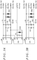
- FIG. 3B and FIG. 4 The same components in FIG. 3B and FIG. 4 as the corresponding components in the embodiment with the redundant sensor are denoted by the same reference numerals and will not be described.
- the Hall IC 25 is omitted as depicted in FIG. 4 and the capacitor C3 and the bi-directional Zener diode ZD3 are omitted as illustrated in FIG. 3B .
- the rest of the configuration in the variation is similar to the corresponding part of the configuration in the embodiment with the redundant sensor.
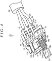
- the sensor unit configured as described above has the single Hall IC 24 and is thus non-redundant, and is assembled into the magnetism collecting module described below.
- the present embodiment has the following features.
- a sensor unit 10 in a second embodiment will be described with reference to FIG. 5 and FIG. 6A .
- the present embodiment includes a redundant sensor.
- Components in the second embodiment that are the same as or correspond to particular components in the above-described embodiment are denoted by the same reference numerals and will not be described below. Parts of the configuration of the second embodiment different from the corresponding parts of the configuration of the above-described embodiment will be described.
- the number of ports in the Hall ICs in the sensor unit 10 is different from the number of ports in the above-described embodiment.
- the second embodiment is the same as the above-described embodiment in the remaining parts of the configuration such as the terminals 11 to 15 and the coupling member 17.
- a Hall IC 24A in the present embodiment has four ports, the power supply input port a1, the ground port d1, and the signal output ports b1, c1, as depicted in FIG. 6A .
- a Hall IC 25A has four ports, the power supply input port a2, the ground port d2, and the signal output ports b2, c2, as depicted in FIG. 6A .
- Leads 24c, 24d are connected to the signal output ports b1, c1 in the Hall IC 24A depicted in FIG. 6A , as illustrated in FIG. 5 , and are connected to lead connection portion 15b by soldering or the like.
- Leads 25c, 25d are connected to the signal output ports b2, c2 in the Hall IC 25A depicted in FIG. 6A , as illustrated in FIG. 5 , and are connected to lead connection portion 11b by soldering or the like.
- the Hall ICs 24A, 25A transmit signals output from the signal output ports b1, c1, b2, c2 by serial communication or CAN communication and share each of the terminals 11, 15.
- the sensor unit 10 configured as described above has the pair of Hall ICs 24A, 25A and is thus redundant, and is assembled into the magnetism collecting module described below.
- FIG. 6B and FIG. 7 The same components in FIG. 6B and FIG. 7 as the corresponding components in the embodiment with the redundant sensor are denoted by the same reference numerals and will not be described.
- the Hall IC 25A is omitted as depicted in FIG. 7
- the capacitor C3 and the bi-directional Zener diode ZD3 are omitted as illustrated in FIG. 3B .
- the rest of the configuration in the variation is similar to the corresponding part of the configuration in the embodiment with the redundant sensor.
- the sensor unit 10 configured as described above has the single Hall IC 24A and is thus non-redundant, and is assembled into the magnetism collecting module described below.
- the present embodiment produces the effects (1) to (3) described in the first embodiment.
- the sensor unit 10 is assembled in the magnetism collecting module used for a torque detecting apparatus serving as a sensor apparatus.
- the torque detecting apparatus has a torsion bar 113 that couples an input shaft 111 and an output shaft 112 together, a permanent magnet 115 coupled to the input shaft 111, a yoke 114 coupled to the output shaft 112, and a tubular magnetism collecting module 118 arranged to surround the yoke 114.
- the torsion bar 113 is coaxially coupled to the input shaft 111 and the output shaft 112. As depicted in FIG.
- the permanent magnet 115 coupled to the input shaft 111 is shaped like a cylinder magnetized to provide, for example, 24 poles (12 N poles and 12 S poles) arranged at regular intervals in a circumferential direction.
- the permanent magnet 115 is coaxially fixed to the input shaft 111.
- the cylindrical yoke 114 is coaxially fixed to the output shaft 112 and arranged so as to surround the permanent magnet 115 with an appropriate radial clearance between the yoke 114 and the permanent magnet 115.
- the yoke 114 includes two magnetic yokes 114A, 114B (soft magnetic materials).
- Each of the magnetic yokes 114A, 114B includes a plate-like ring 116 with 12 pawls 116a arranged circumferentially at regular intervals on a plate surface of the ring 116.
- the pawls 116a are shaped like isosceles triangles and extend in a direction perpendicular to the plate surface.
- the magnetic yokes 114A, 114B are incorporated in a cylindrical synthetic resin body 117 through molding such that the pawls 116a of the magnetic yoke 114A face the pawls 116a of the magnetic yoke 114B so as to be shifted from the pawls 116a of the magnetic yoke 114B at appropriate intervals. As depicted in FIG. 8 , surfaces of the magnetic yokes 114A, 114B that face the permanent magnet 115 are exposed from the synthetic resin body 117.
- the magnetic yokes 114A, 114B are arranged such that, in a neutral state where no torque is applied to the input shaft 111, a tip of each of the pawls 116a points to a boundary between the corresponding N and S poles in the permanent magnet 115.
- the permanent magnet 115 corresponds to a detection object of the Hall ICs 24, 25, and the magnitude of magnetic fields based on the permanent magnet 115 corresponds to the physical quantity of the detection object.
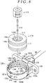
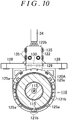
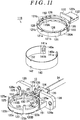
- the magnetism collecting module 118 has two magnetism collecting rings 119A, 119B that are magnetic circuits magnetically coupled to the magnetic yokes 114A, 114B depicted in FIG. 12 to guide each of the magnetic fluxes from the magnetic yokes 114A, 114B to the sensor unit 10.
- the magnetism collecting module 118 includes a first holder 120A and a second holder 120B that hold the magnetism collecting rings 119A, 119B, respectively, and a magnetic shield 140 that covers a circumferentially outer side of each of the magnetism collecting rings 119A, 119B.
- the first holder 120A and the second holder 120B form a magnetism collecting holder.
- the magnetism collecting holder includes the first holder 120A and the second holder 120B resulting from axial division of the magnetism collecting holder into two pieces.
- the first holder 120A is formed of a synthetic resin and has a ring portion 121 shaped like a circular ring and a circuit cover portion 122 shaped like a capped box and integrally coupled to an outer peripheral surface of the ring portion 121 so as to protrude outward in a radial direction.
- the magnetism collecting ring 119A is held in an inner peripheral surface of the ring portion 121 and arranged so as to face an outer peripheral surface of the yoke 114 as depicted in FIG. 9 .
- the magnetism collecting ring 119A is formed of a soft magnetic material. That is, facing surfaces of the magnetic yoke 114A and the magnetism collecting ring 119A are exposed and arranged so as to face each other.
- the second holder 120B is formed of a synthetic resin and has a ring portion 123 shaped like a circular ring and a sensor connection member placement portion 124 shaped like a rectangular plate and integrally coupled to an outer peripheral surface of the ring portion 123 so as to protrude outward in the radial direction.
- the ring portion 123 has an inner peripheral surface and an outer peripheral surface having the same diameters as those of the inner peripheral surface and the outer peripheral surface, respectively, of the ring portion 121 of the first holder 120A.
- the magnetism collecting ring 119B is held in the inner peripheral surface of the ring portion 123 and arranged so as to face the outer peripheral surface of the yoke 114 as depicted in FIG. 9 .
- the magnetism collecting ring 119B is formed of a soft magnetic material. That is, facing surfaces of the magnetic yoke 114B and the magnetism collecting ring 119B are exposed and arranged so as to face each other.
- the outer peripheral surface of the ring portion 123 of the second holder 120B is provided with a plurality of hooking protrusions 125 protruding toward the first holder 120A.
- the hooking protrusions 125 are fitted into respective fitting grooves 126 recessed in the inner peripheral surface of the ring portion 121 of the first holder 120A.
- Engaging pawls 125a at tips of the hooking protrusions 125 are hooked on an axial end surface of the ring portion 121 of the first holder 120A. Consequently, the hooking protrusions 125 are hooked on the ring portion 121 of the first holder 120A to arrange the second holder 120B coaxially with the first holder 120A.
- a periphery of an axial end of the ring portion 123 that is opposite to the first holder is provided with a protrusion 123a for positioning that protrudes outward in the radial direction and a plurality of flange pieces 123b.
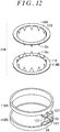
- the two magnetism collecting rings 119A, 119B are arranged parallel to each other and as depicted in FIG.12 , each have flat-plate-like protruding portions 127 such that the distance between the protruding portions 127 of the magnetism collecting ring 119A and the protruding portions 127 of the magnetism collecting ring 119B is shorter than the distance between the remaining part of the magnetism collecting ring 119A and the remaining part of the magnetism collecting ring 119B.
- One of the Hall ICs 24, 25 of the sensor unit 10 or the pair of Hall ICs 24, 25 is inserted into the clearance between the protruding portions 127 of the magnetism collecting rings 119A and the adjacent protruding portions 127 of the magnetism collecting ring 119B.
- the sensor unit 10 is held by the second holder 120B.
- a case with the single Hall IC 24 corresponds to a non-redundant configuration
- a case with the pair of Hall ICs 24, 25 corresponds to a redundant configuration.
- the case with the single Hall IC 24 and the case with the pair of Hall ICs 24, 25 are hereinafter collectively referred to as the Hall IC 24 or the pair of Hall ICs for convenience of explanation.
- the sensor unit 10 is arranged on the sensor connection member placement portion 124. That is, the sensor connection member placement portion 124 is formed, by molding a resin, to accommodate the sensor unit 10 except for the Hall IC 24 or the pair of Hall ICs and the lead connection portions 11b to 15b, 13d.
- the circuit cover portion 122 is placed on the sensor connection member placement portion 124 to form a circuit housing chamber 122a between the circuit cover portion 122 and the sensor connection member placement portion 124 as depicted in FIG. 9 .
- the Hall IC 24 or the pair of Hall ICs is housed in the circuit housing chamber 122a.
- hooking protruding pieces 135 protruding toward the circuit cover portion 122 is provided on side surfaces of the sensor connection member placement portion 124.
- Engaging pawls provided at tips of hooking protruding pieces 135 are locked on edges of a top cover wall 122b of the circuit cover portion 122 to keep the circuit cover portion 122 laid on top of the sensor connection member placement portion 124.
- a pair of flanges 128 is formed to sandwich opposite side surfaces of a base end of the sensor connection member placement portion 124 between the flanges 128.
- a base end of the circuit cover portion 122 is fitted into a clearance formed between the flanges 128.
- a guide groove 129 is formed in each of facing end surfaces of the opposite flanges 128 so as to extend in a direction in which the circuit cover portion 122 is laid on top of the sensor connection member placement portion 124.
- a partition wall 130 formed on the circuit cover portion 122 like a plate is fitted in the guide grooves 129.
- the partition wall 130 is fitted into the guide grooves 129 to guide and place the first holder 120A onto the second holder 120B.
- An attachment hole 128a is formed in each flange 128 so as to penetrate the flange 128 to allow the sensor unit 10 to be attached to a housing (not depicted in the drawings) of an electric power steering system or the like.
- the magnetic shield 140 is fitted over the outer peripheral surface of the ring portion 121 of the first holder 120A and the outer peripheral surface of the ring portion 123 of the second holder 120B.
- the magnetic shield 140 is formed of metal and, for example, shaped by curving a metal plate of steel such that the metal plate has a C-shaped section.
- the magnetic shield 140 is fitted over approximately half the length of the first holder 120A and the second holder 120B in the axial direction to block magnetism in a radial direction of the input shaft 111 and the output shaft 112.
- the magnetic shield 140 is formed to have an axial length slightly larger than a total axial length of the ring portion 121 of the first holder 120A and the ring portion 123 of the second holder 120B. With the engaging pawls 125a of the hooking protrusions 125 hooked on the axial end surface of the ring portion 121 of the first holder 120A, axially opposite ends of the magnetic shield 140 are in abutting contact with the flange pieces 121b of the ring portion 121 and the flange pieces 123b of the ring portion 123.
- the magnetic shield 140 is shaped like a flat plate at circumferentially opposite ends 140a of the magnetic shield 140, and recessed portions 142 for positioning are provided at respective axial ends of a circumferentially substantially central portion of an area of the magnetic shield 140 with the C-shaped section.
- the protrusion 121a of the ring portion 121 and the protrusion 123a of the ring portion 123 are fitted into the recessed portions 142 to position the magnetic shield 140 in the circumferential direction thereof with respect to the first holder 120A and the second holder 120B.
- engaging grooves 150 are formed in areas of the first holder 120A that correspond to the ends 140a of the magnetic shield 140, that is, areas of the first holder 120A that are close to the Hall IC.
- a side opposite to the Hall IC and a side closer to the second holder 120B are open, whereas a side closer to the Hall IC and the remaining part located on a side opposite to the second holder are closed.
- engaging grooves 151 are formed in areas of the second holder 120B that correspond to the ends 140a of the magnetic shield 140, that is, areas of the second holder 120B that are close to the Hall IC.
- a side opposite to the Hall IC and a side closer to the first holder 120A are open, whereas a side closer to the Hall IC and the remaining part located on a side opposite to first holder are closed.
- each of the ends 140a is provided with an engaging member 141a that is in abutting contact with an inner surface of the engaging groove 150 located closer to an axis in a radial direction of the ring portion 121 and an engaging member 141b that is in abutting contact with an inner surface of the engaging groove 151 located closer to the axis in a radial direction of the ring portion 123.
- the engaging members 141a, 141b are elastic and formed by cutting a portion of the magnetic shield 140 and raising the cut portion inward in the radial direction with respect to the ends 140a such that free ends of the engaging members 141a, 141b face each other.
- the engaging members 141a, 141b are elastically locked on the inner surfaces of the engaging grooves 150, 151.
- the present embodiment can provide a torque detecting apparatus having the magnetism collecting module 118 including the sensor unit 10 with a redundant sensor or with no redundant sensor as described in the first embodiment. Regardless of whether or not a redundant sensor is included, the sizes and shapes of the members provided around the sensor unit 10 such as the sensor connection member placement portion 124 are prevented from varying. Thus, the design of these members need not be changed.
- the present embodiment includes a redundant sensor.
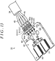
- the sensor unit 10 in the present embodiment has a circuit board 40 (that is, a substrate) serving as a sensor connection member.
- the circuit board 40 is shaped generally like a rectangular plate and has Hall ICs 50, 51 fixedly arranged (that is, mounted) at a tip of the circuit board 40 in a width direction thereof.
- a predetermined circuit pattern 42 is provided that includes capacitors C21 to C24 and bi-directional Zener diodes ZD21, ZD22 illustrated in FIG. 14 as electronic components.
- the Hall ICs 50, 51, the capacitors C21 to C24, and the bi-directional Zener diodes ZD21, ZD22 are electrically connected together.
- Some ports of the Hall ICs 50, 51 are connected to V1, G1, V2, G2. Areas of a circuit provided in the circuit board 40 that are connected to the above-described ports correspond to first connection portions.
- V1 and G1 denote connection terminals for V1 and G1
- V2 and G2 denote connection terminals for V2 and G2 described below.
- G1 and G2 are electrically connected together, but G1 and G2 need not be connected together.
- connection terminals 41 for connection to the harness 34 is arranged in juxtaposition in the width direction.
- the connection terminals 41 include terminals for V1 and G1 provided for the Hall IC 50 and terminals for V2 and G2 provided for the Hall IC 51.
- Each of the connection terminals 41 is folded into an L shape at a base end of the connection terminal 41 and fixedly inserted into a corresponding one of attachment holes 43 formed in the circuit board 40. Tip areas of the folded portions of the connection terminals 41 are arranged parallel to one another so as to extend in a length direction of the connection terminals 41.
- the connection terminals 41 correspond to second connection portions.
- a holding member 44 formed of an insulating synthetic resin is attached to the circuit board 40.
- the holding member 44 has a U shape defined by a pair of leg portions 44a fixed to a flat surface of the circuit board 40 and a coupling portion 44b coupling the leg portions 44a together.
- the coupling portion 44b of the holding member 44 is provided with a plurality of holding portions not depicted in the drawings.
- the holding portions hold the respective connection terminals 41 to arrange the connection terminals 41 parallel to one another with each connection terminal 41 spaced from the adjacent connection terminal 41.
- the holding portions may hold the respective connection terminals 41 by, for example, fitting the connection terminals 41 into the respective holding portions formed as fitting grooves. However, the invention is not limited to this manner of holding the connection terminals 41.
- a bare wire 45a formed by removing a cover from a covered wire 45 located at a terminal of the harness 34 is connected by welding to an area of each connection terminal 41 that extends from the coupling portion 44b toward a side opposite to the circuit board in the length direction of the connection terminal 41.
- the sensor unit 10 configured as described above can be assembled, for example, into the magnetism collecting module 118 in the third embodiment, similarly and alternatively to the sensor unit 10 in the first embodiment.
- FIG. 14B and FIG. 15 The same components in FIG. 14B and FIG. 15 as the corresponding components in the embodiment with the redundant sensor are denoted by the same reference numerals and will not be described.
- the Hall IC 51 is omitted as depicted in FIG. 15 , the capacitors C23, C24 and the bi-directional Zener diode ZD21 are omitted as illustrated in FIG. 14B , and the covered wires 45 connected to the connection terminals 41 (G2), 41 (V2) are omitted.
- the rest of the configuration in the variation is similar to the corresponding part of the configuration in the embodiment with the redundant sensor.
- the above-described sensor unit 10 has only the single Hall IC 50 and is thus non-redundant.
- the sensor unit 10 configured as described above can be assembled, for example, into the magnetism collecting module 118 in the third embodiment, similarly and alternatively to the sensor unit 10 in the first embodiment.
- the embodiments of the invention are not limited to the above-described embodiments but may be varied as follows.
- the magnetic sensor is not limited to the Hall IC but may be another element such as a Hall element, a magneto-resistive element, or a magnetic impedance element.
- the sensor is not limited to the magnetic sensor but may be another sensor.
- the magnetic sensor may be changed to an ultrasonic sensor, an optical sensor, or the like that measures a physical quantity such as the position of the detection object, a distance thereto, or the speed thereof.
- the sensor unit 10 in the first embodiment is used for the magnetism collecting module 118.
- the sensor unit 10 in the second embodiment may be adopted instead of the sensor unit 10 in the first embodiment.
- the arrangement of the sensors in the embodiment described with reference to FIG. 7 is an example in which no redundant sensor is provided. This arrangement is not limited to the non-redundant configuration.
- a pair of sensors for example, Hall ICs
- the two sensors may be electrically connected together as depicted in FIG. 6A
- the apparently single sensor may be arranged similarly to the Hall IC 24A in FIG. 7 , thus providing a redundant sensor.
Landscapes
- Physics & Mathematics (AREA)
- General Physics & Mathematics (AREA)
- Electromagnetism (AREA)
- Transmission And Conversion Of Sensor Element Output (AREA)
- Measuring Magnetic Variables (AREA)
Description
- The invention relates to a sensor unit and a sensor apparatus.
- There has been a demand to provide redundant electric steering systems for automobiles in order to allow vehicles to be automatically driven. Many needs for manual driving of vehicles are still present. To meet both the need for automatic driving and the need for manual driving, two types of structures need to be prepared for torque sensor apparatuses: a structure including a redundant magnetic sensor and a structure including no redundant magnetic sensor, for example, a structure for manual driving.
- Well known torque sensor apparatuses are disclosed in Japanese Patent Application Publication No.
2011-191094 JP 2011-191094 A 2010-271260 JP 2010-271260 A JP 2011-191094 A -
JP 2010-271260 A JP 2010-271260 A - As described above, the disclosure in
JP 2011-191094 A JP 2010-271260 A - The sensor apparatuses including magnetic sensors have been described. However, sensor apparatuses having a sensor different from a magnetic sensor pose a similar problem concerning whether or not a redundant sensor is provided.
- An object of the invention is to provide a sensor unit and a sensor apparatus in which the size of the sensor unit itself is prevented from varying regardless of whether or not a redundant sensor is provided, eliminating the need to change the design of a component to which the sensor unit is attached.
- A sensor unit according to the invention is defined by
independent claim 1. - In this configuration, the sensor connection member is provided with the plurality of the first connection portions and the plurality of the second connection portions so as to enable a plurality of the sensors to be attached to the sensor connection member, or the sensor connection member is provided according to the number of the sensors so as to enable the sensors to be attached to the sensor connection members. Thus, the sensor connection member can accommodate both a configuration with a redundant sensor and a configuration with no redundant sensor.
- In the sensor unit in the above-described aspect of the invention, the sensor connection member may be a terminal formed of a conductive material, and the sensor connection member may be provided according to the number of the sensors so as to enable the sensors to be attached to the sensor connection members. In this configuration, the sensor connection members are provided according to the number of the sensors so as to enable a plurality of the sensors to be attached to the sensor connection members. Thus, the sensor connection members can accommodate both a configuration with a redundant sensor and a configuration with no redundant sensor.
- In the sensor unit in the above-described aspect of the invention, the sensor may be mounted on a substrate serving as the sensor connection member, and the plurality of the first connection portions and the plurality of the second connection portions may be provided on the substrate. In this configuration, the plurality of the first connection portions and the plurality of the second connection portions are provided on the substrate. Thus, the sensor connection member can accommodate both a configuration with a redundant sensor and a configuration with no redundant sensor.
- In the sensor unit in the above-described aspect of the invention, the sensor may be a Hall IC. In this configuration, the sensor unit having the Hall IC allows the above-described effects to be produced.
- A magnetism collecting module in another aspect of the invention includes the sensor unit in the above-described aspect, a magnetic circuit that guides an external magnetic flux to the sensor unit; and a holder that holds the sensor unit and the magnetic circuit.
- A sensor apparatus that detects a torque in yet another aspect of the invention includes the magnetism collecting module in the above-described aspect, a torsion bar that is twisted in response to an applied torque, a cylindrical magnet magnetized to provide a plurality of pairs each of an N pole and an S pole arranged at regular intervals in a circumferential direction, and a yoke that guides a magnetic flux generated by the magnet to the magnetism collecting module.
- In the aspects of the invention, the size of the sensor unit itself is prevented from varying depending on whether or not a redundant sensor is provided. This is effective for eliminating the need to change the design of a component to which the sensor unit is attached.
- The foregoing and further features and advantages of the invention will become apparent from the following description of example embodiments with reference to the accompanying drawings, wherein like numerals are used to represent like elements and wherein:
-
FIG. 1 is a perspective view of a redundant sensor unit in a first embodiment; -
FIG. 2 is a perspective view depicting arrangement of connection terminals; -
FIG. 3A is an electric circuit diagram of the redundant sensor unit in the first embodiment; -
FIG. 3B is an electric circuit diagram of a non-redundant sensor unit; -
FIG. 4 is a perspective view of the non-redundant sensor unit; -
FIG. 5 is a perspective view of a redundant sensor unit in a second embodiment; -
FIG. 6A is an electric circuit diagram of the redundant sensor unit in the second embodiment; -
FIG. 6B is an electric circuit diagram of a non-redundant sensor unit; -
FIG. 7 is a perspective view of the non-redundant sensor unit; -
FIG. 8 is an exploded perspective view of a torque sensor in a third embodiment; -
FIG. 9 is a longitudinal sectional view of the torque sensor and a magnetism collecting module in the third embodiment; -
FIG. 10 is a plan view of the magnetism collecting module in the third embodiment; -
FIG. 11 is a perspective view of the magnetism collecting module in the third embodiment; -
FIG. 12 is a diagram illustrating a configurational relation between magnetism collecting rings and sensors in the third embodiment; -
FIG. 13 is a perspective view of a redundant sensor unit in a fourth embodiment; -
FIG. 14A is an electric circuit diagram of the redundant sensor unit; -
FIG. 14B is an electric circuit diagram of a non-redundant sensor unit; and -
FIG. 15 is a perspective view of the non-redundant sensor unit. - A
sensor unit 10 in a first embodiment in which the invention is embodied will be described below with reference toFIGS. 1 to 3A . - As depicted in
FIG. 1 , thesensor unit 10 has a plurality ofterminals 11 to 15 arranged in parallel with one another, acoupling member 17 formed of a synthetic resin to couple theterminals 11 to 15 together, andHall ICs terminals 11 to 15 to serve as magnetic sensors. Theterminals 11 to 15 correspond to sensor connection members. Theterminals 11 to 15 are formed of a conductive material shaped like plates and have a predetermined strength needed to hold thesensor unit 10. Theterminals 11 to 15 are formed, for example, by cutting out a copper plate. - The
terminals 11 to 15 havemain portions 11a to 15a, respectively, arranged substantially parallel to one another and positioned flush with the same virtual plane and leadconnection portions 11b to 15b, respectively, located at tips of theterminals 11 to 15 so as to extend in an extending direction of themain portions 11a to 15a. - The
lead connection portion 13b of the terminal 13 expands toward the terminal 14 in a width direction of thelead connection portion 13b to form alead connection portion 13d. Thelead connection portions main portions lead connection portions FIG. 1 andFIG. 2 so as to form step portions. - The
lead connection portion 11b of the terminal 11 is formed like a crank with respect to themain portion 11a and biased toward theadjacent terminal 12. Thelead connection portions - Opposite ends of a
bridging piece 16 in the width direction are integrally coupled to the tip of thelead connection portion 12b of the terminal 12 and the tip of thelead connection portion 14b of the terminal 14, respectively, viastep portions piece 16 is formed to lie below themain portions - As depicted in
FIG. 1 andFIG. 2 ,cable connection portions 11c to 13c, 15c extend from themain portions 11a to 13a, 15a of theterminals 11 to 13 and the terminal 15 toward aharness 34 to serve as second connection portions. Thecable connection portion 15c is formed like a crank with respect to themain portion 11a and biased toward thecable connection portion 13c. - As depicted in
FIG. 1 , abare wire portion 18a of asignal cable 18 is connected to thecable connection portion 11c by welding or the like. Abare wire portion 19a of aground cable 19 is connected to thecable connection portion 12c by welding or the like. Abare wire portion 20a of apower supply cable 20 is connected to thecable connection portion 13c by welding or the like. Abare wire portion 21a of asignal cable 21 is connected to thecable connection portion 15c by welding or the like. Theharness 34 is a covered bundle of thesignal cable 18, theground cable 19, thepower supply cable 20, and thesignal cable 21. - As depicted in
FIG. 3A , each of theHall ICs FIG. 1 , leads 24a, 25a are connected to the power supply input ports of theHall ICs lead connection portions Leads Hall ICs lead connection portions Leads Hall ICs lead connection portions - The
coupling member 17 is formed to substantially entirely cover themain portions 11a to 15a of theterminals 11 to 15 by molding a synthetic resin, and in thecoupling member 17, capacitors C1 to C3 and bi-directional Zener diodes ZD1 to ZD3 depicted inFIG. 3A are embedded. The capacitor C1 and the bi-directional Zener diode ZD1 illustrated inFIG. 3A are connected in parallel with each other between themain portion 15a of the terminal 15 and themain portion 14a of the terminal 14. The capacitor C2 and the bi-directional Zener diode ZD2 illustrated inFIG. 3A are connected in parallel with each other between themain portion 13a of the terminal 13 and themain portion 12a of the terminal 12. The capacitor C3 and the bi-directional Zener diode ZD3 illustrated inFIG. 3A are connected in parallel with each other between themain portion 11a of the terminal 11 and themain portion 12a of the terminal 12. Theterminals 11 to 15, theHall ICs coupling member 17 are connected together as described above to provide thesensor unit 10 having the circuit illustrated inFIG. 3A . Thesensor unit 10 configured as described above has the pair ofHall ICs - Now, a variation with a non-redundant configuration will be described with reference to
FIG. 3B andFIG. 4 . The same components inFIG. 3B andFIG. 4 as the corresponding components in the embodiment with the redundant sensor are denoted by the same reference numerals and will not be described. - When no redundant Hall IC is provided, the
Hall IC 25 is omitted as depicted inFIG. 4 and the capacitor C3 and the bi-directional Zener diode ZD3 are omitted as illustrated inFIG. 3B . The rest of the configuration in the variation is similar to the corresponding part of the configuration in the embodiment with the redundant sensor. - The sensor unit configured as described above has the
single Hall IC 24 and is thus non-redundant, and is assembled into the magnetism collecting module described below. - The present embodiment has the following features.
- (1) In the
sensor unit 10 in the present embodiment, theterminals 11 to 15, serving as the sensor connection members, are provided with thelead connection portions Hall ICs 24, 25 (sensors) can be attached and thecable connection portions 11c to 13c, 15c (second connection portions) connected to the outside. Theterminals 11 to 15 are provided according to the number of sensors so as to enable theHall ICs terminals 11 to 15. The leads to theHall IC 24 corresponding to at least one magnetic sensor are connected to theterminals 11 to 15 (sensor connection members). Thus, theterminals 11 to 15 (sensor connection members) can accommodate both a configuration with a redundant sensor and a configuration with no redundant sensor. - (2) In the
sensor unit 10 in the present embodiment, the sensor connection members are the terminals, and the terminals are provided according to the number of theHall ICs - (3) In the
sensor unit 10 in the present embodiment, the sensors are Hall ICs. As a result, the sensor unit with the Hall ICs produces effects described in (1) and (2). - Now, a
sensor unit 10 in a second embodiment will be described with reference toFIG. 5 andFIG. 6A . The present embodiment includes a redundant sensor. Components in the second embodiment that are the same as or correspond to particular components in the above-described embodiment are denoted by the same reference numerals and will not be described below. Parts of the configuration of the second embodiment different from the corresponding parts of the configuration of the above-described embodiment will be described. - In the present embodiment, the number of ports in the Hall ICs in the
sensor unit 10 is different from the number of ports in the above-described embodiment. The second embodiment is the same as the above-described embodiment in the remaining parts of the configuration such as theterminals 11 to 15 and thecoupling member 17. AHall IC 24A in the present embodiment has four ports, the power supply input port a1, the ground port d1, and the signal output ports b1, c1, as depicted inFIG. 6A . AHall IC 25A has four ports, the power supply input port a2, the ground port d2, and the signal output ports b2, c2, as depicted inFIG. 6A . -
Leads Hall IC 24A depicted inFIG. 6A , as illustrated inFIG. 5 , and are connected to leadconnection portion 15b by soldering or the like.Leads Hall IC 25A depicted inFIG. 6A , as illustrated inFIG. 5 , and are connected to leadconnection portion 11b by soldering or the like. - Connections to the power supply ports a1, a2 and the ground ports d1, d2 are similar to the corresponding connections in the above-described embodiment and will not be described. In the present embodiment, the
Hall ICs terminals sensor unit 10 configured as described above has the pair ofHall ICs - Now, a variation with a non-redundant configuration will be described with reference to
FIG. 6B andFIG. 7 . The same components inFIG. 6B andFIG. 7 as the corresponding components in the embodiment with the redundant sensor are denoted by the same reference numerals and will not be described. When no redundant Hall IC is provided, theHall IC 25A is omitted as depicted inFIG. 7 , and the capacitor C3 and the bi-directional Zener diode ZD3 are omitted as illustrated inFIG. 3B . The rest of the configuration in the variation is similar to the corresponding part of the configuration in the embodiment with the redundant sensor. - The
sensor unit 10 configured as described above has thesingle Hall IC 24A and is thus non-redundant, and is assembled into the magnetism collecting module described below. The present embodiment produces the effects (1) to (3) described in the first embodiment. - Now, with reference to
FIGS. 8 to 12 , a third embodiment will be described in which thesensor unit 10 is assembled in the magnetism collecting module used for a torque detecting apparatus serving as a sensor apparatus. - As depicted in
FIG. 8 andFIG. 9 , the torque detecting apparatus has atorsion bar 113 that couples an input shaft 111 and anoutput shaft 112 together, apermanent magnet 115 coupled to the input shaft 111, ayoke 114 coupled to theoutput shaft 112, and a tubularmagnetism collecting module 118 arranged to surround theyoke 114. As depicted inFIG. 9 , thetorsion bar 113 is coaxially coupled to the input shaft 111 and theoutput shaft 112. As depicted inFIG. 9 , thepermanent magnet 115 coupled to the input shaft 111 is shaped like a cylinder magnetized to provide, for example, 24 poles (12 N poles and 12 S poles) arranged at regular intervals in a circumferential direction. Thepermanent magnet 115 is coaxially fixed to the input shaft 111. As depicted inFIG. 9 , thecylindrical yoke 114 is coaxially fixed to theoutput shaft 112 and arranged so as to surround thepermanent magnet 115 with an appropriate radial clearance between theyoke 114 and thepermanent magnet 115. - As depicted in
FIG. 9 andFIG. 12 , theyoke 114 includes twomagnetic yokes magnetic yokes like ring 116 with 12pawls 116a arranged circumferentially at regular intervals on a plate surface of thering 116. Thepawls 116a are shaped like isosceles triangles and extend in a direction perpendicular to the plate surface. Themagnetic yokes synthetic resin body 117 through molding such that thepawls 116a of themagnetic yoke 114A face thepawls 116a of themagnetic yoke 114B so as to be shifted from thepawls 116a of themagnetic yoke 114B at appropriate intervals. As depicted inFIG. 8 , surfaces of themagnetic yokes permanent magnet 115 are exposed from thesynthetic resin body 117. Themagnetic yokes pawls 116a points to a boundary between the corresponding N and S poles in thepermanent magnet 115. Thepermanent magnet 115 corresponds to a detection object of theHall ICs permanent magnet 115 corresponds to the physical quantity of the detection object. - As depicted in
FIG. 8 , themagnetism collecting module 118 has two magnetism collecting rings 119A, 119B that are magnetic circuits magnetically coupled to themagnetic yokes FIG. 12 to guide each of the magnetic fluxes from themagnetic yokes sensor unit 10. Themagnetism collecting module 118 includes afirst holder 120A and asecond holder 120B that hold the magnetism collecting rings 119A, 119B, respectively, and amagnetic shield 140 that covers a circumferentially outer side of each of the magnetism collecting rings 119A, 119B. Thefirst holder 120A and thesecond holder 120B form a magnetism collecting holder. That is, the magnetism collecting holder includes thefirst holder 120A and thesecond holder 120B resulting from axial division of the magnetism collecting holder into two pieces. As depicted inFIG. 11 , thefirst holder 120A is formed of a synthetic resin and has aring portion 121 shaped like a circular ring and acircuit cover portion 122 shaped like a capped box and integrally coupled to an outer peripheral surface of thering portion 121 so as to protrude outward in a radial direction. Themagnetism collecting ring 119A is held in an inner peripheral surface of thering portion 121 and arranged so as to face an outer peripheral surface of theyoke 114 as depicted inFIG. 9 . Themagnetism collecting ring 119A is formed of a soft magnetic material. That is, facing surfaces of themagnetic yoke 114A and themagnetism collecting ring 119A are exposed and arranged so as to face each other. - As depicted in
FIG. 8 andFIG. 11 , a periphery of an axial end of thering portion 121 that is opposite to the second holder is provided with aprotrusion 121a for positioning that protrudes outward in the radial direction and a plurality offlange pieces 121b. As depicted inFIG. 11 , thesecond holder 120B is formed of a synthetic resin and has aring portion 123 shaped like a circular ring and a sensor connectionmember placement portion 124 shaped like a rectangular plate and integrally coupled to an outer peripheral surface of thering portion 123 so as to protrude outward in the radial direction. Thering portion 123 has an inner peripheral surface and an outer peripheral surface having the same diameters as those of the inner peripheral surface and the outer peripheral surface, respectively, of thering portion 121 of thefirst holder 120A. Themagnetism collecting ring 119B is held in the inner peripheral surface of thering portion 123 and arranged so as to face the outer peripheral surface of theyoke 114 as depicted inFIG. 9 . Themagnetism collecting ring 119B is formed of a soft magnetic material. That is, facing surfaces of themagnetic yoke 114B and themagnetism collecting ring 119B are exposed and arranged so as to face each other. - As depicted in
FIG. 11 , the outer peripheral surface of thering portion 123 of thesecond holder 120B is provided with a plurality of hookingprotrusions 125 protruding toward thefirst holder 120A. The hookingprotrusions 125 are fitted into respectivefitting grooves 126 recessed in the inner peripheral surface of thering portion 121 of thefirst holder 120A. Engagingpawls 125a at tips of the hookingprotrusions 125 are hooked on an axial end surface of thering portion 121 of thefirst holder 120A. Consequently, the hookingprotrusions 125 are hooked on thering portion 121 of thefirst holder 120A to arrange thesecond holder 120B coaxially with thefirst holder 120A. As depicted inFIG. 8 andFIG. 11 , a periphery of an axial end of thering portion 123 that is opposite to the first holder is provided with aprotrusion 123a for positioning that protrudes outward in the radial direction and a plurality offlange pieces 123b. - As depicted in
FIG. 8 , the two magnetism collecting rings 119A, 119B are arranged parallel to each other and as depicted inFIG.12 , each have flat-plate-like protrudingportions 127 such that the distance between the protrudingportions 127 of themagnetism collecting ring 119A and the protrudingportions 127 of themagnetism collecting ring 119B is shorter than the distance between the remaining part of themagnetism collecting ring 119A and the remaining part of themagnetism collecting ring 119B. One of theHall ICs sensor unit 10 or the pair ofHall ICs portions 127 of the magnetism collecting rings 119A and the adjacent protrudingportions 127 of themagnetism collecting ring 119B. Thesensor unit 10 is held by thesecond holder 120B. A case with thesingle Hall IC 24 corresponds to a non-redundant configuration, and a case with the pair ofHall ICs single Hall IC 24 and the case with the pair ofHall ICs Hall IC 24 or the pair of Hall ICs for convenience of explanation. - As depicted in
FIG. 11 , thesensor unit 10 is arranged on the sensor connectionmember placement portion 124. That is, the sensor connectionmember placement portion 124 is formed, by molding a resin, to accommodate thesensor unit 10 except for theHall IC 24 or the pair of Hall ICs and thelead connection portions 11b to 15b, 13d. Thecircuit cover portion 122 is placed on the sensor connectionmember placement portion 124 to form acircuit housing chamber 122a between thecircuit cover portion 122 and the sensor connectionmember placement portion 124 as depicted inFIG. 9 . TheHall IC 24 or the pair of Hall ICs is housed in thecircuit housing chamber 122a. - As depicted in
FIG. 8 andFIG. 11 , hooking protrudingpieces 135 protruding toward thecircuit cover portion 122 is provided on side surfaces of the sensor connectionmember placement portion 124. Engaging pawls provided at tips of hooking protrudingpieces 135 are locked on edges of atop cover wall 122b of thecircuit cover portion 122 to keep thecircuit cover portion 122 laid on top of the sensor connectionmember placement portion 124. - As depicted in
FIG. 8 andFIG. 11 , a pair offlanges 128 is formed to sandwich opposite side surfaces of a base end of the sensor connectionmember placement portion 124 between theflanges 128. As depicted inFIG. 8 andFIG. 10 , a base end of thecircuit cover portion 122 is fitted into a clearance formed between theflanges 128. - A
guide groove 129 is formed in each of facing end surfaces of theopposite flanges 128 so as to extend in a direction in which thecircuit cover portion 122 is laid on top of the sensor connectionmember placement portion 124. Apartition wall 130 formed on thecircuit cover portion 122 like a plate is fitted in theguide grooves 129. When thecircuit cover portion 122 is placed onto the sensor connectionmember placement portion 124, thepartition wall 130 is fitted into theguide grooves 129 to guide and place thefirst holder 120A onto thesecond holder 120B. Anattachment hole 128a is formed in eachflange 128 so as to penetrate theflange 128 to allow thesensor unit 10 to be attached to a housing (not depicted in the drawings) of an electric power steering system or the like. - As depicted in
FIG. 8 andFIG. 11 , themagnetic shield 140 is fitted over the outer peripheral surface of thering portion 121 of thefirst holder 120A and the outer peripheral surface of thering portion 123 of thesecond holder 120B. Themagnetic shield 140 is formed of metal and, for example, shaped by curving a metal plate of steel such that the metal plate has a C-shaped section. Themagnetic shield 140 is fitted over approximately half the length of thefirst holder 120A and thesecond holder 120B in the axial direction to block magnetism in a radial direction of the input shaft 111 and theoutput shaft 112. Themagnetic shield 140 is formed to have an axial length slightly larger than a total axial length of thering portion 121 of thefirst holder 120A and thering portion 123 of thesecond holder 120B. With the engaging pawls 125a of the hookingprotrusions 125 hooked on the axial end surface of thering portion 121 of thefirst holder 120A, axially opposite ends of themagnetic shield 140 are in abutting contact with theflange pieces 121b of thering portion 121 and theflange pieces 123b of thering portion 123. Themagnetic shield 140 is shaped like a flat plate at circumferentially opposite ends 140a of themagnetic shield 140, and recessedportions 142 for positioning are provided at respective axial ends of a circumferentially substantially central portion of an area of themagnetic shield 140 with the C-shaped section. Theprotrusion 121a of thering portion 121 and theprotrusion 123a of thering portion 123 are fitted into the recessedportions 142 to position themagnetic shield 140 in the circumferential direction thereof with respect to thefirst holder 120A and thesecond holder 120B. - As depicted in
FIG. 11 , engaginggrooves 150 are formed in areas of thefirst holder 120A that correspond to theends 140a of themagnetic shield 140, that is, areas of thefirst holder 120A that are close to the Hall IC. For the engaginggrooves 150 in thefirst holder 120A, in the circumferential direction of thering portion 121, a side opposite to the Hall IC and a side closer to thesecond holder 120B are open, whereas a side closer to the Hall IC and the remaining part located on a side opposite to the second holder are closed. - As depicted in
FIG. 11 , engaginggrooves 151 are formed in areas of thesecond holder 120B that correspond to theends 140a of themagnetic shield 140, that is, areas of thesecond holder 120B that are close to the Hall IC. For the engaginggrooves 151 in thesecond holder 120B, in the circumferential direction of thering portion 123, a side opposite to the Hall IC and a side closer to thefirst holder 120A are open, whereas a side closer to the Hall IC and the remaining part located on a side opposite to first holder are closed. - As depicted in
FIG. 11 , the circumferential ends 140a of themagnetic shield 140 are inserted into the respectiveengaging grooves FIG. 11 , each of theends 140a is provided with an engagingmember 141a that is in abutting contact with an inner surface of the engaginggroove 150 located closer to an axis in a radial direction of thering portion 121 and an engagingmember 141b that is in abutting contact with an inner surface of the engaginggroove 151 located closer to the axis in a radial direction of thering portion 123. The engagingmembers magnetic shield 140 and raising the cut portion inward in the radial direction with respect to theends 140a such that free ends of the engagingmembers members grooves - The present embodiment can provide a torque detecting apparatus having the
magnetism collecting module 118 including thesensor unit 10 with a redundant sensor or with no redundant sensor as described in the first embodiment. Regardless of whether or not a redundant sensor is included, the sizes and shapes of the members provided around thesensor unit 10 such as the sensor connectionmember placement portion 124 are prevented from varying. Thus, the design of these members need not be changed. - Now, a fourth embodiment of the
sensor unit 10 will be described with reference toFIG. 13 andFIG. 14A . The present embodiment includes a redundant sensor. - As depicted in
FIG. 13 , thesensor unit 10 in the present embodiment has a circuit board 40 (that is, a substrate) serving as a sensor connection member. Thecircuit board 40 is shaped generally like a rectangular plate and hasHall ICs circuit board 40 in a width direction thereof. On a portion of a surface of thecircuit board 40 located between the tip and a base end thereof, apredetermined circuit pattern 42 is provided that includes capacitors C21 to C24 and bi-directional Zener diodes ZD21, ZD22 illustrated inFIG. 14 as electronic components. - As depicted in
FIG. 14A , in thecircuit pattern 42, theHall ICs Hall ICs circuit board 40 that are connected to the above-described ports correspond to first connection portions. InFIG. 14A , V1 and G1 denote connection terminals for V1 and G1, and V2 and G2 denote connection terminals for V2 and G2 described below. In the present embodiment, G1 and G2 are electrically connected together, but G1 and G2 need not be connected together. - At a base end of the
circuit board 40, a plurality ofconnection terminals 41 for connection to theharness 34 is arranged in juxtaposition in the width direction. Theconnection terminals 41 include terminals for V1 and G1 provided for theHall IC 50 and terminals for V2 and G2 provided for theHall IC 51. Each of theconnection terminals 41 is folded into an L shape at a base end of theconnection terminal 41 and fixedly inserted into a corresponding one of attachment holes 43 formed in thecircuit board 40. Tip areas of the folded portions of theconnection terminals 41 are arranged parallel to one another so as to extend in a length direction of theconnection terminals 41. Theconnection terminals 41 correspond to second connection portions. - As depicted in
FIG. 13 , a holdingmember 44 formed of an insulating synthetic resin is attached to thecircuit board 40. The holdingmember 44 has a U shape defined by a pair ofleg portions 44a fixed to a flat surface of thecircuit board 40 and acoupling portion 44b coupling theleg portions 44a together. Thecoupling portion 44b of the holdingmember 44 is provided with a plurality of holding portions not depicted in the drawings. The holding portions hold therespective connection terminals 41 to arrange theconnection terminals 41 parallel to one another with eachconnection terminal 41 spaced from theadjacent connection terminal 41. The holding portions may hold therespective connection terminals 41 by, for example, fitting theconnection terminals 41 into the respective holding portions formed as fitting grooves. However, the invention is not limited to this manner of holding theconnection terminals 41. - As depicted in
FIG. 13 , abare wire 45a formed by removing a cover from a coveredwire 45 located at a terminal of theharness 34 is connected by welding to an area of eachconnection terminal 41 that extends from thecoupling portion 44b toward a side opposite to the circuit board in the length direction of theconnection terminal 41. - The
sensor unit 10 configured as described above can be assembled, for example, into themagnetism collecting module 118 in the third embodiment, similarly and alternatively to thesensor unit 10 in the first embodiment. - Now, a variation with a non-redundant configuration will be described with reference to
FIG. 14B andFIG. 15 . The same components inFIG. 14B andFIG. 15 as the corresponding components in the embodiment with the redundant sensor are denoted by the same reference numerals and will not be described. - When no redundant Hall IC is provided, the
Hall IC 51 is omitted as depicted inFIG. 15 , the capacitors C23, C24 and the bi-directional Zener diode ZD21 are omitted as illustrated inFIG. 14B , and the coveredwires 45 connected to the connection terminals 41 (G2), 41 (V2) are omitted. The rest of the configuration in the variation is similar to the corresponding part of the configuration in the embodiment with the redundant sensor. The above-describedsensor unit 10 has only thesingle Hall IC 50 and is thus non-redundant. - The
sensor unit 10 configured as described above can be assembled, for example, into themagnetism collecting module 118 in the third embodiment, similarly and alternatively to thesensor unit 10 in the first embodiment. - The embodiments of the invention are not limited to the above-described embodiments but may be varied as follows. The magnetic sensor is not limited to the Hall IC but may be another element such as a Hall element, a magneto-resistive element, or a magnetic impedance element. The sensor is not limited to the magnetic sensor but may be another sensor. For example, the magnetic sensor may be changed to an ultrasonic sensor, an optical sensor, or the like that measures a physical quantity such as the position of the detection object, a distance thereto, or the speed thereof.
- In the third embodiment, the
sensor unit 10 in the first embodiment is used for themagnetism collecting module 118. However, thesensor unit 10 in the second embodiment may be adopted instead of thesensor unit 10 in the first embodiment. - The arrangement of the sensors in the embodiment described with reference to
FIG. 7 is an example in which no redundant sensor is provided. This arrangement is not limited to the non-redundant configuration. A pair of sensors (for example, Hall ICs) may be integrally formed using a mold, the two sensors may be electrically connected together as depicted inFIG. 6A , while the apparently single sensor may be arranged similarly to theHall IC 24A inFIG. 7 , thus providing a redundant sensor.
Claims (4)
- A sensor unit comprising:a sensor (24, 25; 24A, 25A; 50, 51) that detects a physical quantity related to a detection object (115);a sensor connection member (11, 12, 13, 14, 15; 40) having at least a first connection portion (11b, 12b, 13b, 13d, 14b, 15b) to which a lead to the sensor (24, 25; 24A, 25A; 50, 51) is connected and a second connection portion (11c, 12c,.13c, 15c; 41) electrically connected to the first connection portion (11b, 12b, 13b, 13d, 14b, 15b; 42) and electrically connected to an outside of the sensor unit (10); andan electronic component (C1-C3, ZD1-ZD3; C21-C24, ZD21, ZD22) provided in a circuit between the first connection portion (11b, 12b, 13b, 13d, 14b, 15b) and the second connection portion (11c, 12c,.13c, 15c; 41),whereinthe sensor connection member (40) includes a plurality of the first connection portions and a plurality of the second connection portions (41) so as to enable a plurality of the sensors (50; 51) to be attached to the sensor connection member (40), wherein the sensor connection member (40) is a circuit board, at least one sensor (50, 51) is mounted on the circuit board (40), and the plurality of the first connection portions and the plurality of the second connection portions (41) are provided on the circuit board; ora plurality of the sensor connection members (11, 12, 13, 14, 15) are provided according to a number of the sensors (24, 25; 24A, 25A) so as to enable the sensors (24, 25; 24A, 25A) to be attached to the sensor connection members (11, 12, 13, 14, 15), wherein the sensor connection members (11, 12, 13, 14, 15) are arranged in parallel to each other, with each sensor connection member (11, 12, 13, 14, 15) being a terminal that is formed of a conductive material in form of a plate; and a lead to at least one of the sensors (24, 25; 24A, 25A) is connected to the sensor connection members (11, 12, 13, 14, 15).
- The sensor unit according to claim 1, wherein,
the sensor (24, 25; 24A, 25A; 50, 51) is a Hall IC. - A magnetism collecting module comprising:the sensor unit (10) according to claim 2;a magnetic circuit (119A, 119B) that guides an external magnetic flux to the sensor unit (10); anda holder (120A, 120B) that holds the sensor unit (10) and the magnetic circuit (119A, 119B).
- A sensor apparatus that detects a torque, the sensor apparatus comprising:the magnetism collecting module (118) according to claim 3;a torsion bar (113) that is twisted in response to an applied torque;a cylindrical magnet (115) magnetized to provide a plurality of pairs each of an N pole and an S pole arranged at regular intervals in a circumferential direction; anda yoke that guides a magnetic flux generated by the magnet (115) to the magnetism collecting module (118).
Applications Claiming Priority (1)
| Application Number | Priority Date | Filing Date | Title |
|---|---|---|---|
| JP2016100715A JP6759704B2 (en) | 2016-05-19 | 2016-05-19 | Sensor unit and sensor device |
Publications (2)
| Publication Number | Publication Date |
|---|---|
| EP3246666A1 EP3246666A1 (en) | 2017-11-22 |
| EP3246666B1 true EP3246666B1 (en) | 2019-05-08 |
Family
ID=58709345
Family Applications (1)
| Application Number | Title | Priority Date | Filing Date |
|---|---|---|---|
| EP17171017.1A Active EP3246666B1 (en) | 2016-05-19 | 2017-05-15 | Sensor unit and magnetism collecting module and sensor apparatus |
Country Status (4)
| Country | Link |
|---|---|
| US (1) | US10048143B2 (en) |
| EP (1) | EP3246666B1 (en) |
| JP (1) | JP6759704B2 (en) |
| CN (1) | CN107402094B (en) |
Families Citing this family (8)
| Publication number | Priority date | Publication date | Assignee | Title |
|---|---|---|---|---|
| JP6547778B2 (en) * | 2016-08-23 | 2019-07-24 | 株式会社デンソー | Position detection device |
| JP7127417B2 (en) | 2018-08-09 | 2022-08-30 | 株式会社ジェイテクト | sensor device |
| JP2020035778A (en) * | 2018-08-27 | 2020-03-05 | 株式会社ジェイテクト | Resin molded product, sensor device, and method of manufacturing resin molded product |
| JP7081527B2 (en) * | 2019-02-25 | 2022-06-07 | 株式会社デンソー | Magnetic sensor and torque detector using it |
| JP7293818B2 (en) | 2019-04-03 | 2023-06-20 | 株式会社プロテリアル | Sensor devices, cables with sensors and composite cables |
| JP7228100B2 (en) * | 2019-09-25 | 2023-02-24 | 株式会社プロテリアル | Sensor device, multicore wire with sensor, composite cable, and method for manufacturing multicore wire with sensor |
| JP2022130102A (en) * | 2021-02-25 | 2022-09-06 | 株式会社ジェイテクト | Magnetic shield, sensor device, and method for assembling magnetic shield |
| DE102021108659A1 (en) * | 2021-04-07 | 2022-11-03 | Robert Bosch Gesellschaft mit beschränkter Haftung | Sensor unit and method of manufacturing a sensor unit |
Family Cites Families (18)
| Publication number | Priority date | Publication date | Assignee | Title |
|---|---|---|---|---|
| JPH08254172A (en) * | 1995-03-17 | 1996-10-01 | Mitsubishi Electric Corp | Rotation angle detecting device |
| JP3603406B2 (en) * | 1995-09-11 | 2004-12-22 | 株式会社デンソー | Magnetic detection sensor and method of manufacturing the same |
| DE20018538U1 (en) * | 2000-10-27 | 2002-03-07 | Mannesmann Vdo Ag | sensor module |
| JP2003329523A (en) * | 2002-03-07 | 2003-11-19 | Denso Corp | Torque sensor |
| JP2004332633A (en) * | 2003-05-08 | 2004-11-25 | Aisan Ind Co Ltd | Throttle control device |
| FR2872896B1 (en) * | 2004-07-09 | 2008-01-11 | Moving Magnet Tech | POSITION SENSOR, PARTICULARLY FOR MEASURING THE TORSION OF A STEERING COLUMN |
| JP5183036B2 (en) * | 2006-06-23 | 2013-04-17 | 株式会社ジェイテクト | Torque detection device and method for manufacturing yoke assembly |
| US7639004B2 (en) * | 2007-07-23 | 2009-12-29 | Gm Global Technology Operations, Inc. | Apparatus for sensing angular displacement between first and second rotating shafts including flux collectors |
| DE102009006529A1 (en) * | 2009-01-28 | 2010-08-26 | Continental Automotive Gmbh | position sensor |
| JP2010271260A (en) | 2009-05-25 | 2010-12-02 | Hitachi Cable Ltd | Terminal for torque sensor, and torque sensor using the same |
| JP5067676B2 (en) * | 2010-03-12 | 2012-11-07 | 株式会社デンソー | Sensor unit and magnetism collecting module |
| US8448528B2 (en) * | 2010-09-27 | 2013-05-28 | Bourns Incorporated | Three-piece torque sensor assembly |
| DE102010047128A1 (en) * | 2010-09-30 | 2012-04-05 | Infineon Technologies Ag | Hall sensor arrangement for redundantly measuring a magnetic field |
| US9105485B2 (en) * | 2013-03-08 | 2015-08-11 | Taiwan Semiconductor Manufacturing Company, Ltd. | Bonding structures and methods of forming the same |
| JP2014238355A (en) * | 2013-06-10 | 2014-12-18 | 日立金属株式会社 | On-vehicle detection device |
| JP6160298B2 (en) * | 2013-06-26 | 2017-07-12 | 株式会社ジェイテクト | Torque detection device, electric power steering device including the torque detection device, and torque detection device calibration method |
| JP6171694B2 (en) * | 2013-08-02 | 2017-08-02 | 株式会社ジェイテクト | Torque detection device and electric power steering device |
| JP6311926B2 (en) * | 2014-06-18 | 2018-04-18 | 株式会社ジェイテクト | Torque sensor and electric power steering device |
-
2016
- 2016-05-19 JP JP2016100715A patent/JP6759704B2/en active Active
-
2017
- 2017-05-11 US US15/592,278 patent/US10048143B2/en active Active
- 2017-05-15 EP EP17171017.1A patent/EP3246666B1/en active Active
- 2017-05-19 CN CN201710356055.XA patent/CN107402094B/en active Active
Non-Patent Citations (1)
| Title |
|---|
| None * |
Also Published As
| Publication number | Publication date |
|---|---|
| JP2017207402A (en) | 2017-11-24 |
| US20170336276A1 (en) | 2017-11-23 |
| EP3246666A1 (en) | 2017-11-22 |
| CN107402094B (en) | 2021-11-16 |
| JP6759704B2 (en) | 2020-09-23 |
| US10048143B2 (en) | 2018-08-14 |
| CN107402094A (en) | 2017-11-28 |
Similar Documents
| Publication | Publication Date | Title |
|---|---|---|
| EP3246666B1 (en) | Sensor unit and magnetism collecting module and sensor apparatus | |
| JP5403792B2 (en) | Current detector assembly structure | |
| US10060808B2 (en) | Torque detector | |
| US8421451B2 (en) | Assembly structure of current detection device | |
| US9086440B2 (en) | Current sensor | |
| JP2009139272A (en) | Current sensor | |
| US11187601B2 (en) | Sensor device | |
| US11394267B2 (en) | Motor | |
| JP6472897B2 (en) | Electrical connector kit, electronic component, and assembly method | |
| JP5225884B2 (en) | Assembling structure and assembling method of current detection device | |
| JP5331082B2 (en) | connector | |
| EP3681017A1 (en) | Motor | |
| EP0909011B1 (en) | Connection structure of stepping motor | |
| US10408598B2 (en) | Proximity sensor | |
| JP2019139874A (en) | Connector structure for vehicle mounted device | |
| US11536594B2 (en) | Sensor component, pre-assembly arrangement for a sensor component, and method for producing a sensor component | |
| KR100838055B1 (en) | Sensor for detecting electric current | |
| KR20210077405A (en) | Motor | |
| KR20160124332A (en) | Current sensor module with integrally modularized a magnetic core and a hall sensor integrated circuit, and current sensor box for car battery with the same | |
| JP2016206015A (en) | Bus bar assembled current sensor | |
| JP4733527B2 (en) | Connection structure between stepping motor and circuit board | |
| JP2021032796A (en) | Current sensor | |
| CN110400686B (en) | Coil component | |
| EP3324195A1 (en) | Electronic component | |
| CN115039518A (en) | Motor driving device and method for manufacturing the same |
Legal Events
| Date | Code | Title | Description |
|---|---|---|---|
| PUAI | Public reference made under article 153(3) epc to a published international application that has entered the european phase |
Free format text: ORIGINAL CODE: 0009012 |
|
| STAA | Information on the status of an ep patent application or granted ep patent |
Free format text: STATUS: THE APPLICATION HAS BEEN PUBLISHED |
|
| AK | Designated contracting states |
Kind code of ref document: A1 Designated state(s): AL AT BE BG CH CY CZ DE DK EE ES FI FR GB GR HR HU IE IS IT LI LT LU LV MC MK MT NL NO PL PT RO RS SE SI SK SM TR |
|
| AX | Request for extension of the european patent |
Extension state: BA ME |
|
| STAA | Information on the status of an ep patent application or granted ep patent |
Free format text: STATUS: REQUEST FOR EXAMINATION WAS MADE |
|
| 17P | Request for examination filed |
Effective date: 20180514 |
|
| RBV | Designated contracting states (corrected) |
Designated state(s): AL AT BE BG CH CY CZ DE DK EE ES FI FR GB GR HR HU IE IS IT LI LT LU LV MC MK MT NL NO PL PT RO RS SE SI SK SM TR |
|
| GRAP | Despatch of communication of intention to grant a patent |
Free format text: ORIGINAL CODE: EPIDOSNIGR1 |
|
| STAA | Information on the status of an ep patent application or granted ep patent |
Free format text: STATUS: GRANT OF PATENT IS INTENDED |
|
| INTG | Intention to grant announced |
Effective date: 20181126 |
|
| GRAS | Grant fee paid |
Free format text: ORIGINAL CODE: EPIDOSNIGR3 |
|
| GRAA | (expected) grant |
Free format text: ORIGINAL CODE: 0009210 |
|
| STAA | Information on the status of an ep patent application or granted ep patent |
Free format text: STATUS: THE PATENT HAS BEEN GRANTED |
|
| AK | Designated contracting states |
Kind code of ref document: B1 Designated state(s): AL AT BE BG CH CY CZ DE DK EE ES FI FR GB GR HR HU IE IS IT LI LT LU LV MC MK MT NL NO PL PT RO RS SE SI SK SM TR |
|
| REG | Reference to a national code |
Ref country code: GB Ref legal event code: FG4D |
|
| RIN1 | Information on inventor provided before grant (corrected) |
Inventor name: ASANO, TAKATSUGU Inventor name: TOYAMA, YUICHI |
|
| REG | Reference to a national code |
Ref country code: CH Ref legal event code: EP Ref country code: AT Ref legal event code: REF Ref document number: 1130868 Country of ref document: AT Kind code of ref document: T Effective date: 20190515 |
|
| REG | Reference to a national code |
Ref country code: DE Ref legal event code: R096 Ref document number: 602017003776 Country of ref document: DE Ref country code: IE Ref legal event code: FG4D |
|
| REG | Reference to a national code |
Ref country code: NL Ref legal event code: MP Effective date: 20190508 |
|
| REG | Reference to a national code |
Ref country code: LT Ref legal event code: MG4D |
|
| PG25 | Lapsed in a contracting state [announced via postgrant information from national office to epo] |
Ref country code: NO Free format text: LAPSE BECAUSE OF FAILURE TO SUBMIT A TRANSLATION OF THE DESCRIPTION OR TO PAY THE FEE WITHIN THE PRESCRIBED TIME-LIMIT Effective date: 20190808 Ref country code: LT Free format text: LAPSE BECAUSE OF FAILURE TO SUBMIT A TRANSLATION OF THE DESCRIPTION OR TO PAY THE FEE WITHIN THE PRESCRIBED TIME-LIMIT Effective date: 20190508 Ref country code: ES Free format text: LAPSE BECAUSE OF FAILURE TO SUBMIT A TRANSLATION OF THE DESCRIPTION OR TO PAY THE FEE WITHIN THE PRESCRIBED TIME-LIMIT Effective date: 20190508 Ref country code: SE Free format text: LAPSE BECAUSE OF FAILURE TO SUBMIT A TRANSLATION OF THE DESCRIPTION OR TO PAY THE FEE WITHIN THE PRESCRIBED TIME-LIMIT Effective date: 20190508 Ref country code: NL Free format text: LAPSE BECAUSE OF FAILURE TO SUBMIT A TRANSLATION OF THE DESCRIPTION OR TO PAY THE FEE WITHIN THE PRESCRIBED TIME-LIMIT Effective date: 20190508 Ref country code: PT Free format text: LAPSE BECAUSE OF FAILURE TO SUBMIT A TRANSLATION OF THE DESCRIPTION OR TO PAY THE FEE WITHIN THE PRESCRIBED TIME-LIMIT Effective date: 20190908 Ref country code: HR Free format text: LAPSE BECAUSE OF FAILURE TO SUBMIT A TRANSLATION OF THE DESCRIPTION OR TO PAY THE FEE WITHIN THE PRESCRIBED TIME-LIMIT Effective date: 20190508 Ref country code: AL Free format text: LAPSE BECAUSE OF FAILURE TO SUBMIT A TRANSLATION OF THE DESCRIPTION OR TO PAY THE FEE WITHIN THE PRESCRIBED TIME-LIMIT Effective date: 20190508 Ref country code: FI Free format text: LAPSE BECAUSE OF FAILURE TO SUBMIT A TRANSLATION OF THE DESCRIPTION OR TO PAY THE FEE WITHIN THE PRESCRIBED TIME-LIMIT Effective date: 20190508 |
|
| PG25 | Lapsed in a contracting state [announced via postgrant information from national office to epo] |
Ref country code: LV Free format text: LAPSE BECAUSE OF FAILURE TO SUBMIT A TRANSLATION OF THE DESCRIPTION OR TO PAY THE FEE WITHIN THE PRESCRIBED TIME-LIMIT Effective date: 20190508 Ref country code: GR Free format text: LAPSE BECAUSE OF FAILURE TO SUBMIT A TRANSLATION OF THE DESCRIPTION OR TO PAY THE FEE WITHIN THE PRESCRIBED TIME-LIMIT Effective date: 20190809 Ref country code: BG Free format text: LAPSE BECAUSE OF FAILURE TO SUBMIT A TRANSLATION OF THE DESCRIPTION OR TO PAY THE FEE WITHIN THE PRESCRIBED TIME-LIMIT Effective date: 20190808 Ref country code: RS Free format text: LAPSE BECAUSE OF FAILURE TO SUBMIT A TRANSLATION OF THE DESCRIPTION OR TO PAY THE FEE WITHIN THE PRESCRIBED TIME-LIMIT Effective date: 20190508 |
|
| REG | Reference to a national code |
Ref country code: AT Ref legal event code: MK05 Ref document number: 1130868 Country of ref document: AT Kind code of ref document: T Effective date: 20190508 |
|
| PG25 | Lapsed in a contracting state [announced via postgrant information from national office to epo] |
Ref country code: CZ Free format text: LAPSE BECAUSE OF FAILURE TO SUBMIT A TRANSLATION OF THE DESCRIPTION OR TO PAY THE FEE WITHIN THE PRESCRIBED TIME-LIMIT Effective date: 20190508 Ref country code: SK Free format text: LAPSE BECAUSE OF FAILURE TO SUBMIT A TRANSLATION OF THE DESCRIPTION OR TO PAY THE FEE WITHIN THE PRESCRIBED TIME-LIMIT Effective date: 20190508 Ref country code: RO Free format text: LAPSE BECAUSE OF FAILURE TO SUBMIT A TRANSLATION OF THE DESCRIPTION OR TO PAY THE FEE WITHIN THE PRESCRIBED TIME-LIMIT Effective date: 20190508 Ref country code: DK Free format text: LAPSE BECAUSE OF FAILURE TO SUBMIT A TRANSLATION OF THE DESCRIPTION OR TO PAY THE FEE WITHIN THE PRESCRIBED TIME-LIMIT Effective date: 20190508 Ref country code: AT Free format text: LAPSE BECAUSE OF FAILURE TO SUBMIT A TRANSLATION OF THE DESCRIPTION OR TO PAY THE FEE WITHIN THE PRESCRIBED TIME-LIMIT Effective date: 20190508 Ref country code: EE Free format text: LAPSE BECAUSE OF FAILURE TO SUBMIT A TRANSLATION OF THE DESCRIPTION OR TO PAY THE FEE WITHIN THE PRESCRIBED TIME-LIMIT Effective date: 20190508 |
|
| REG | Reference to a national code |
Ref country code: BE Ref legal event code: MM Effective date: 20190531 |
|
| REG | Reference to a national code |
Ref country code: DE Ref legal event code: R097 Ref document number: 602017003776 Country of ref document: DE |
|
| PG25 | Lapsed in a contracting state [announced via postgrant information from national office to epo] |
Ref country code: IT Free format text: LAPSE BECAUSE OF FAILURE TO SUBMIT A TRANSLATION OF THE DESCRIPTION OR TO PAY THE FEE WITHIN THE PRESCRIBED TIME-LIMIT Effective date: 20190508 Ref country code: LU Free format text: LAPSE BECAUSE OF NON-PAYMENT OF DUE FEES Effective date: 20190515 Ref country code: MC Free format text: LAPSE BECAUSE OF FAILURE TO SUBMIT A TRANSLATION OF THE DESCRIPTION OR TO PAY THE FEE WITHIN THE PRESCRIBED TIME-LIMIT Effective date: 20190508 Ref country code: SM Free format text: LAPSE BECAUSE OF FAILURE TO SUBMIT A TRANSLATION OF THE DESCRIPTION OR TO PAY THE FEE WITHIN THE PRESCRIBED TIME-LIMIT Effective date: 20190508 |
|
| PLBE | No opposition filed within time limit |
Free format text: ORIGINAL CODE: 0009261 |
|
| STAA | Information on the status of an ep patent application or granted ep patent |
Free format text: STATUS: NO OPPOSITION FILED WITHIN TIME LIMIT |
|
| PG25 | Lapsed in a contracting state [announced via postgrant information from national office to epo] |
Ref country code: TR Free format text: LAPSE BECAUSE OF FAILURE TO SUBMIT A TRANSLATION OF THE DESCRIPTION OR TO PAY THE FEE WITHIN THE PRESCRIBED TIME-LIMIT Effective date: 20190508 |
|
| 26N | No opposition filed |
Effective date: 20200211 |
|
| PG25 | Lapsed in a contracting state [announced via postgrant information from national office to epo] |
Ref country code: IE Free format text: LAPSE BECAUSE OF NON-PAYMENT OF DUE FEES Effective date: 20190515 Ref country code: PL Free format text: LAPSE BECAUSE OF FAILURE TO SUBMIT A TRANSLATION OF THE DESCRIPTION OR TO PAY THE FEE WITHIN THE PRESCRIBED TIME-LIMIT Effective date: 20190508 |
|
| PG25 | Lapsed in a contracting state [announced via postgrant information from national office to epo] |
Ref country code: BE Free format text: LAPSE BECAUSE OF NON-PAYMENT OF DUE FEES Effective date: 20190531 Ref country code: SI Free format text: LAPSE BECAUSE OF FAILURE TO SUBMIT A TRANSLATION OF THE DESCRIPTION OR TO PAY THE FEE WITHIN THE PRESCRIBED TIME-LIMIT Effective date: 20190508 |
|
| PG25 | Lapsed in a contracting state [announced via postgrant information from national office to epo] |
Ref country code: CH Free format text: LAPSE BECAUSE OF NON-PAYMENT OF DUE FEES Effective date: 20200531 Ref country code: LI Free format text: LAPSE BECAUSE OF NON-PAYMENT OF DUE FEES Effective date: 20200531 |
|
| PG25 | Lapsed in a contracting state [announced via postgrant information from national office to epo] |
Ref country code: CY Free format text: LAPSE BECAUSE OF FAILURE TO SUBMIT A TRANSLATION OF THE DESCRIPTION OR TO PAY THE FEE WITHIN THE PRESCRIBED TIME-LIMIT Effective date: 20190508 |
|
| PG25 | Lapsed in a contracting state [announced via postgrant information from national office to epo] |
Ref country code: IS Free format text: LAPSE BECAUSE OF FAILURE TO SUBMIT A TRANSLATION OF THE DESCRIPTION OR TO PAY THE FEE WITHIN THE PRESCRIBED TIME-LIMIT Effective date: 20190908 |
|
| PG25 | Lapsed in a contracting state [announced via postgrant information from national office to epo] |
Ref country code: MT Free format text: LAPSE BECAUSE OF FAILURE TO SUBMIT A TRANSLATION OF THE DESCRIPTION OR TO PAY THE FEE WITHIN THE PRESCRIBED TIME-LIMIT Effective date: 20190508 Ref country code: HU Free format text: LAPSE BECAUSE OF FAILURE TO SUBMIT A TRANSLATION OF THE DESCRIPTION OR TO PAY THE FEE WITHIN THE PRESCRIBED TIME-LIMIT; INVALID AB INITIO Effective date: 20170515 |
|
| GBPC | Gb: european patent ceased through non-payment of renewal fee |
Effective date: 20210515 |
|
| PG25 | Lapsed in a contracting state [announced via postgrant information from national office to epo] |
Ref country code: GB Free format text: LAPSE BECAUSE OF NON-PAYMENT OF DUE FEES Effective date: 20210515 |
|
| PG25 | Lapsed in a contracting state [announced via postgrant information from national office to epo] |
Ref country code: MK Free format text: LAPSE BECAUSE OF FAILURE TO SUBMIT A TRANSLATION OF THE DESCRIPTION OR TO PAY THE FEE WITHIN THE PRESCRIBED TIME-LIMIT Effective date: 20190508 |
|
| REG | Reference to a national code |
Ref country code: FR Ref legal event code: PLFP Year of fee payment: 7 |
|
| PGFP | Annual fee paid to national office [announced via postgrant information from national office to epo] |
Ref country code: FR Payment date: 20230411 Year of fee payment: 7 Ref country code: DE Payment date: 20230331 Year of fee payment: 7 |