EP3245665B1 - Method for producing a nonplanar wafer - Google Patents
Method for producing a nonplanar wafer Download PDFInfo
- Publication number
- EP3245665B1 EP3245665B1 EP16700464.7A EP16700464A EP3245665B1 EP 3245665 B1 EP3245665 B1 EP 3245665B1 EP 16700464 A EP16700464 A EP 16700464A EP 3245665 B1 EP3245665 B1 EP 3245665B1
- Authority
- EP
- European Patent Office
- Prior art keywords
- solid
- state
- state component
- coating
- component
- Prior art date
- Legal status (The legal status is an assumption and is not a legal conclusion. Google has not performed a legal analysis and makes no representation as to the accuracy of the status listed.)
- Active
Links
- 238000004519 manufacturing process Methods 0.000 title description 16
- 238000000576 coating method Methods 0.000 claims description 33
- 239000011248 coating agent Substances 0.000 claims description 31
- 239000000463 material Substances 0.000 claims description 20
- 230000004048 modification Effects 0.000 claims description 19
- 238000012986 modification Methods 0.000 claims description 19
- 230000005855 radiation Effects 0.000 claims description 17
- 239000013078 crystal Substances 0.000 claims description 15
- 238000000034 method Methods 0.000 claims description 15
- 229920000642 polymer Polymers 0.000 claims description 9
- 239000004205 dimethyl polysiloxane Substances 0.000 claims description 8
- 229920000435 poly(dimethylsiloxane) Polymers 0.000 claims description 8
- 230000035882 stress Effects 0.000 claims description 8
- 238000011282 treatment Methods 0.000 claims description 7
- 230000009477 glass transition Effects 0.000 claims description 4
- 230000008646 thermal stress Effects 0.000 claims description 3
- 235000013870 dimethyl polysiloxane Nutrition 0.000 claims 1
- CXQXSVUQTKDNFP-UHFFFAOYSA-N octamethyltrisiloxane Chemical compound C[Si](C)(C)O[Si](C)(C)O[Si](C)(C)C CXQXSVUQTKDNFP-UHFFFAOYSA-N 0.000 claims 1
- 238000004987 plasma desorption mass spectroscopy Methods 0.000 claims 1
- 239000007787 solid Substances 0.000 description 130
- 235000012431 wafers Nutrition 0.000 description 27
- 230000007547 defect Effects 0.000 description 13
- 239000000919 ceramic Substances 0.000 description 6
- 238000001816 cooling Methods 0.000 description 5
- 239000004065 semiconductor Substances 0.000 description 5
- JBRZTFJDHDCESZ-UHFFFAOYSA-N AsGa Chemical compound [As]#[Ga] JBRZTFJDHDCESZ-UHFFFAOYSA-N 0.000 description 3
- 229910002601 GaN Inorganic materials 0.000 description 3
- XUIMIQQOPSSXEZ-UHFFFAOYSA-N Silicon Chemical compound [Si] XUIMIQQOPSSXEZ-UHFFFAOYSA-N 0.000 description 3
- 229910052594 sapphire Inorganic materials 0.000 description 3
- 239000010980 sapphire Substances 0.000 description 3
- 238000000926 separation method Methods 0.000 description 3
- 229910052710 silicon Inorganic materials 0.000 description 3
- 239000010703 silicon Substances 0.000 description 3
- HBMJWWWQQXIZIP-UHFFFAOYSA-N silicon carbide Chemical compound [Si+]#[C-] HBMJWWWQQXIZIP-UHFFFAOYSA-N 0.000 description 3
- IJGRMHOSHXDMSA-UHFFFAOYSA-N Atomic nitrogen Chemical compound N#N IJGRMHOSHXDMSA-UHFFFAOYSA-N 0.000 description 2
- 229910001218 Gallium arsenide Inorganic materials 0.000 description 2
- 238000010521 absorption reaction Methods 0.000 description 2
- PNEYBMLMFCGWSK-UHFFFAOYSA-N aluminium oxide Inorganic materials [O-2].[O-2].[O-2].[Al+3].[Al+3] PNEYBMLMFCGWSK-UHFFFAOYSA-N 0.000 description 2
- JNDMLEXHDPKVFC-UHFFFAOYSA-N aluminum;oxygen(2-);yttrium(3+) Chemical compound [O-2].[O-2].[O-2].[Al+3].[Y+3] JNDMLEXHDPKVFC-UHFFFAOYSA-N 0.000 description 2
- 229910010293 ceramic material Inorganic materials 0.000 description 2
- 230000008859 change Effects 0.000 description 2
- 229910052593 corundum Inorganic materials 0.000 description 2
- 238000000354 decomposition reaction Methods 0.000 description 2
- 230000001419 dependent effect Effects 0.000 description 2
- 238000000407 epitaxy Methods 0.000 description 2
- 230000000977 initiatory effect Effects 0.000 description 2
- 238000005468 ion implantation Methods 0.000 description 2
- 229910052751 metal Inorganic materials 0.000 description 2
- 239000002184 metal Substances 0.000 description 2
- 230000003287 optical effect Effects 0.000 description 2
- 230000000737 periodic effect Effects 0.000 description 2
- -1 polydimethylsiloxane Polymers 0.000 description 2
- 230000008569 process Effects 0.000 description 2
- 229910010271 silicon carbide Inorganic materials 0.000 description 2
- 230000006641 stabilisation Effects 0.000 description 2
- 238000011105 stabilization Methods 0.000 description 2
- 239000012780 transparent material Substances 0.000 description 2
- 229910001845 yogo sapphire Inorganic materials 0.000 description 2
- 229910019901 yttrium aluminum garnet Inorganic materials 0.000 description 2
- JMASRVWKEDWRBT-UHFFFAOYSA-N Gallium nitride Chemical compound [Ga]#N JMASRVWKEDWRBT-UHFFFAOYSA-N 0.000 description 1
- WHXSMMKQMYFTQS-UHFFFAOYSA-N Lithium Chemical compound [Li] WHXSMMKQMYFTQS-UHFFFAOYSA-N 0.000 description 1
- FYYHWMGAXLPEAU-UHFFFAOYSA-N Magnesium Chemical compound [Mg] FYYHWMGAXLPEAU-UHFFFAOYSA-N 0.000 description 1
- 229910000577 Silicon-germanium Inorganic materials 0.000 description 1
- RTAQQCXQSZGOHL-UHFFFAOYSA-N Titanium Chemical compound [Ti] RTAQQCXQSZGOHL-UHFFFAOYSA-N 0.000 description 1
- 229910002113 barium titanate Inorganic materials 0.000 description 1
- JRPBQTZRNDNNOP-UHFFFAOYSA-N barium titanate Chemical compound [Ba+2].[Ba+2].[O-][Ti]([O-])([O-])[O-] JRPBQTZRNDNNOP-UHFFFAOYSA-N 0.000 description 1
- AOWKSNWVBZGMTJ-UHFFFAOYSA-N calcium titanate Chemical compound [Ca+2].[O-][Ti]([O-])=O AOWKSNWVBZGMTJ-UHFFFAOYSA-N 0.000 description 1
- 238000006243 chemical reaction Methods 0.000 description 1
- 238000013461 design Methods 0.000 description 1
- 238000011161 development Methods 0.000 description 1
- 238000005516 engineering process Methods 0.000 description 1
- 230000005284 excitation Effects 0.000 description 1
- 229910000154 gallium phosphate Inorganic materials 0.000 description 1
- 238000000227 grinding Methods 0.000 description 1
- 238000010438 heat treatment Methods 0.000 description 1
- 238000013532 laser treatment Methods 0.000 description 1
- 229910052745 lead Inorganic materials 0.000 description 1
- 239000007788 liquid Substances 0.000 description 1
- 229910052744 lithium Inorganic materials 0.000 description 1
- GQYHUHYESMUTHG-UHFFFAOYSA-N lithium niobate Chemical compound [Li+].[O-][Nb](=O)=O GQYHUHYESMUTHG-UHFFFAOYSA-N 0.000 description 1
- 238000011068 loading method Methods 0.000 description 1
- 238000003754 machining Methods 0.000 description 1
- 229910052749 magnesium Inorganic materials 0.000 description 1
- 239000011777 magnesium Substances 0.000 description 1
- 230000007246 mechanism Effects 0.000 description 1
- 239000003607 modifier Substances 0.000 description 1
- 229910052757 nitrogen Inorganic materials 0.000 description 1
- 238000012545 processing Methods 0.000 description 1
- 230000001902 propagating effect Effects 0.000 description 1
- 230000001681 protective effect Effects 0.000 description 1
- 239000010453 quartz Substances 0.000 description 1
- 229910052761 rare earth metal Inorganic materials 0.000 description 1
- 150000002910 rare earth metals Chemical class 0.000 description 1
- VYPSYNLAJGMNEJ-UHFFFAOYSA-N silicon dioxide Inorganic materials O=[Si]=O VYPSYNLAJGMNEJ-UHFFFAOYSA-N 0.000 description 1
- 239000011343 solid material Substances 0.000 description 1
- 238000000859 sublimation Methods 0.000 description 1
- 230000008022 sublimation Effects 0.000 description 1
- 239000000758 substrate Substances 0.000 description 1
- 239000002887 superconductor Substances 0.000 description 1
- 238000010897 surface acoustic wave method Methods 0.000 description 1
- 229910021521 yttrium barium copper oxide Inorganic materials 0.000 description 1
Images


Classifications
-
- B—PERFORMING OPERATIONS; TRANSPORTING
- B23—MACHINE TOOLS; METAL-WORKING NOT OTHERWISE PROVIDED FOR
- B23K—SOLDERING OR UNSOLDERING; WELDING; CLADDING OR PLATING BY SOLDERING OR WELDING; CUTTING BY APPLYING HEAT LOCALLY, e.g. FLAME CUTTING; WORKING BY LASER BEAM
- B23K26/00—Working by laser beam, e.g. welding, cutting or boring
- B23K26/50—Working by transmitting the laser beam through or within the workpiece
- B23K26/53—Working by transmitting the laser beam through or within the workpiece for modifying or reforming the material inside the workpiece, e.g. for producing break initiation cracks
-
- B—PERFORMING OPERATIONS; TRANSPORTING
- B28—WORKING CEMENT, CLAY, OR STONE
- B28D—WORKING STONE OR STONE-LIKE MATERIALS
- B28D1/00—Working stone or stone-like materials, e.g. brick, concrete or glass, not provided for elsewhere; Machines, devices, tools therefor
- B28D1/22—Working stone or stone-like materials, e.g. brick, concrete or glass, not provided for elsewhere; Machines, devices, tools therefor by cutting, e.g. incising
- B28D1/221—Working stone or stone-like materials, e.g. brick, concrete or glass, not provided for elsewhere; Machines, devices, tools therefor by cutting, e.g. incising by thermic methods
-
- B—PERFORMING OPERATIONS; TRANSPORTING
- B23—MACHINE TOOLS; METAL-WORKING NOT OTHERWISE PROVIDED FOR
- B23K—SOLDERING OR UNSOLDERING; WELDING; CLADDING OR PLATING BY SOLDERING OR WELDING; CUTTING BY APPLYING HEAT LOCALLY, e.g. FLAME CUTTING; WORKING BY LASER BEAM
- B23K26/00—Working by laser beam, e.g. welding, cutting or boring
- B23K26/02—Positioning or observing the workpiece, e.g. with respect to the point of impact; Aligning, aiming or focusing the laser beam
- B23K26/06—Shaping the laser beam, e.g. by masks or multi-focusing
- B23K26/062—Shaping the laser beam, e.g. by masks or multi-focusing by direct control of the laser beam
- B23K26/0622—Shaping the laser beam, e.g. by masks or multi-focusing by direct control of the laser beam by shaping pulses
- B23K26/0624—Shaping the laser beam, e.g. by masks or multi-focusing by direct control of the laser beam by shaping pulses using ultrashort pulses, i.e. pulses of 1ns or less
-
- H—ELECTRICITY
- H01—ELECTRIC ELEMENTS
- H01L—SEMICONDUCTOR DEVICES NOT COVERED BY CLASS H10
- H01L21/00—Processes or apparatus adapted for the manufacture or treatment of semiconductor or solid state devices or of parts thereof
- H01L21/02—Manufacture or treatment of semiconductor devices or of parts thereof
- H01L21/02002—Preparing wafers
-
- H—ELECTRICITY
- H01—ELECTRIC ELEMENTS
- H01L—SEMICONDUCTOR DEVICES NOT COVERED BY CLASS H10
- H01L21/00—Processes or apparatus adapted for the manufacture or treatment of semiconductor or solid state devices or of parts thereof
- H01L21/02—Manufacture or treatment of semiconductor devices or of parts thereof
- H01L21/04—Manufacture or treatment of semiconductor devices or of parts thereof the devices having potential barriers, e.g. a PN junction, depletion layer or carrier concentration layer
- H01L21/18—Manufacture or treatment of semiconductor devices or of parts thereof the devices having potential barriers, e.g. a PN junction, depletion layer or carrier concentration layer the devices having semiconductor bodies comprising elements of Group IV of the Periodic Table or AIIIBV compounds with or without impurities, e.g. doping materials
- H01L21/30—Treatment of semiconductor bodies using processes or apparatus not provided for in groups H01L21/20 - H01L21/26
- H01L21/302—Treatment of semiconductor bodies using processes or apparatus not provided for in groups H01L21/20 - H01L21/26 to change their surface-physical characteristics or shape, e.g. etching, polishing, cutting
-
- B—PERFORMING OPERATIONS; TRANSPORTING
- B23—MACHINE TOOLS; METAL-WORKING NOT OTHERWISE PROVIDED FOR
- B23K—SOLDERING OR UNSOLDERING; WELDING; CLADDING OR PLATING BY SOLDERING OR WELDING; CUTTING BY APPLYING HEAT LOCALLY, e.g. FLAME CUTTING; WORKING BY LASER BEAM
- B23K2101/00—Articles made by soldering, welding or cutting
- B23K2101/36—Electric or electronic devices
- B23K2101/40—Semiconductor devices
-
- B—PERFORMING OPERATIONS; TRANSPORTING
- B23—MACHINE TOOLS; METAL-WORKING NOT OTHERWISE PROVIDED FOR
- B23K—SOLDERING OR UNSOLDERING; WELDING; CLADDING OR PLATING BY SOLDERING OR WELDING; CUTTING BY APPLYING HEAT LOCALLY, e.g. FLAME CUTTING; WORKING BY LASER BEAM
- B23K2103/00—Materials to be soldered, welded or cut
- B23K2103/50—Inorganic material, e.g. metals, not provided for in B23K2103/02 – B23K2103/26
- B23K2103/52—Ceramics
-
- B—PERFORMING OPERATIONS; TRANSPORTING
- B23—MACHINE TOOLS; METAL-WORKING NOT OTHERWISE PROVIDED FOR
- B23K—SOLDERING OR UNSOLDERING; WELDING; CLADDING OR PLATING BY SOLDERING OR WELDING; CUTTING BY APPLYING HEAT LOCALLY, e.g. FLAME CUTTING; WORKING BY LASER BEAM
- B23K2103/00—Materials to be soldered, welded or cut
- B23K2103/50—Inorganic material, e.g. metals, not provided for in B23K2103/02 – B23K2103/26
- B23K2103/56—Inorganic material, e.g. metals, not provided for in B23K2103/02 – B23K2103/26 semiconducting
-
- B—PERFORMING OPERATIONS; TRANSPORTING
- B23—MACHINE TOOLS; METAL-WORKING NOT OTHERWISE PROVIDED FOR
- B23K—SOLDERING OR UNSOLDERING; WELDING; CLADDING OR PLATING BY SOLDERING OR WELDING; CUTTING BY APPLYING HEAT LOCALLY, e.g. FLAME CUTTING; WORKING BY LASER BEAM
- B23K26/00—Working by laser beam, e.g. welding, cutting or boring
- B23K26/36—Removing material
- B23K26/40—Removing material taking account of the properties of the material involved
Definitions
- the present invention relates to a method for separating at least one part of a solid from a solid.
- Wafers are usually parts of a solid that have been separated from a solid. They essentially extend in two dimensions, ie their thickness is at least one order of magnitude smaller than their width and length. Wafers are preferably used in semiconductor technology for the production of solar cells, computer chips, LEDs, etc.
- the production of wafers is very cost-intensive, which means that attempts are made to obtain as many wafers as possible from a solid body. This causes the wafers to become thinner, which in turn causes them to deform after a coating if the thermal expansion coefficients of the coating and the wafer vary.
- Such a deformation is referred to as a warp, which describes a curvature of the wafer.
- Such bulges are, for example, by the publications EP0966047A2 , US6528394 , US6829270 , US7315045 and US7592629 , the objects of which are made the subject of the present protective right document by reference.
- the deformations of the wafer mean that the multi-layer arrangement produced cannot be optimally processed or that it cannot only be subjected to limited forces or that it extends further in the height direction than is absolutely necessary.
- the U.S. 2014/038392 A1 describes a method for separating a layer of crystalline semiconductor material from a thicker wafer using laser beams.
- the separated layer comprises, for example, an optical, photovoltaic, electronic, or microelectronic-mechanical system.
- the EP 3 137 657 A0 ( WO 2015 165552 A1 ) describes a method for separating a three-dimensional solid layer from a solid.
- the method comprises creating a defect layer within the solid body by means of a laser beam and detaching the solid body layer along the defect layer from the solid body.
- the solid portion is preferably produced in such a way that it assumes the desired shape as a result of subsequent processing. It is thus in Depending on the material properties of the solids portion and the coating, the solids portion is produced with a mold through which the deformation resulting from the coating is utilized in order to create a preferably flat or essentially flat surface of the multilayer arrangement at least on the one hand and preferably on both sides.
- the modifications are produced within the crystal lattice of the solid by means of radiation from at least one laser, in particular a picosecond or femtosecond laser, introduced via an outer surface of the solid portion into the interior of the solid portion.
- the modifications in the crystal lattice are produced by ion implantation. This embodiment is advantageous since modifications can be produced very precisely by means of laser radiation and ion implantation. The detachment area can thus be generated very easily depending on the respective parameters.
- the individual modifications or defects or damaged areas result from multi-photon excitation brought about by the laser, in particular a femtosecond laser or a picosecond laser.
- the laser preferably has a pulse duration of less than 10 ps, particularly preferably less than 1 ps and most preferably less than 500 fs.
- the energy of the laser beam, in particular of the fs laser is selected in such a way that the damage propagation in the solid body or in the crystal is less than three times the Reyleigh length, preferably less than the Reyleigh length and particularly preferably less than one third is the Reyleigh length.
- the wavelength of the laser beam, in particular of the fs laser is selected in such a way that the absorption of the solid body or the material is less than 10 cm -1 and preferably less than 1 cm -1 and particularly preferably less than 0 .1 cm -1 .
- the further treatment comprises the arrangement or production of a coating on at least one surface of the solid portion.
- the specified parameters include at least data by which the thermal expansion coefficients of the material of the solid portion and of the coating are included.
- the parameters preferably comprise data by which the thickness/height (preferably average thickness/height) and/or the width and/or the length and/or the shape of the solid fraction and/or the coating is/are included. This embodiment is advantageous because it allows solid parts to be produced very precisely for different material combinations (solid and coating).
- the solid or the workpiece preferably has a material or a material combination from one of the main groups 3, 4 and 5 of the periodic table of the elements, such as Si, SiC, SiGe, Ge, GaAs, InP, GaN, Al2O3 (sapphire), AlN .
- the solid particularly preferably has a combination of elements occurring in the third and fifth group of the periodic table.
- Conceivable materials or material combinations are, for example, gallium arsenide, silicon, silicon carbide, etc.
- the solid body can have a ceramic (e.g.
- Al2O3 - aluminum oxide or consist of a ceramic
- preferred ceramics are, for example, perovskite ceramics (such as Pb, O, Ti / Zr-containing ceramics) in general and lead magnesium niobates, barium titanate, lithium titanate, yttrium aluminum garnet, in particular yttrium aluminum garnet crystals for solid state laser applications, SAW ceramics (surface acoustic wave), such as lithium niobate, gallium orthophosphate, Quartz, calcium titanate, etc. in particular.
- the solid body thus preferably has a semiconductor material or a ceramic material, or the solid body particularly preferably consists of at least one semiconductor material or a ceramic material.
- the solid body has a transparent material or partially consists or is made of a transparent material, such as sapphire.
- Other materials that can be considered here as solid material alone or in combination with another material are, for example, "wide band gap" materials, InAISb, high-temperature superconductors, in particular rare earth cuprates (eg YBa2Cu3O7).
- the solid body is additionally or alternatively conceivable for the solid body to be a photomask, with the photomask material in the present case preferably being any photomask material known on the date of application and particularly preferably combinations thereof being able to be used.
- the crystal lattice formed in the course of the detachment region is changed, in particular damaged.
- This embodiment is advantageous because the crystal lattice can be changed or defects, in particular microcracks, can be produced in such a way that the forces required to separate the solid portion from the solid can be set, e.g. by the laser impingement. It is therefore possible within the meaning of the present invention for the crystal structure in the detachment region to be modified or damaged by means of laser radiation in such a way that the solid portion detaches or is separated from the solid as a result of the laser treatment.
- the detachment of the solid portion from the solid body comprises at least the steps of arranging a receiving layer on the solid body to hold the solid portion, and subjecting the receiving layer to thermal stress to, in particular mechanically, generate stresses in the solid body, wherein the stresses propagate a crack in the solid along the detachment region, separating the solid portion from the solid.
- This embodiment is advantageous because forces for separating the solid portion from the solid can be generated very precisely and in a defined manner.
- the recording layer has or consists of a polymer, in particular PDMS, with the thermal loading taking place in such a way that the polymer undergoes a glass transition.
- the receiving layer preferably consists of polydimethylsiloxane (PDMS) or has polydimethylsiloxane (PDMS).
- PDMS polydimethylsiloxane
- PDMS polydimethylsiloxane
- the thermal impact preferably represents a cooling of the recording layer to or below the ambient temperature and preferably below 10° C. and particularly preferably below 0° C. and more preferably below -10° C.
- the cooling of the recording layer which is preferably designed as a polymer layer, is most preferably carried out in such a way that that at least part of the receiving layer, which preferably has PDMS or consists of it, undergoes a glass transition.
- the cooling can be cooling to below -100° C., which can be effected, for example, by means of liquid nitrogen.
- the object is also achieved by a method for producing a multilayer arrangement.
- the method for producing the multilayer arrangement comprises at least the following steps: providing a wafer, in particular a curved one, with a first uneven shape; arranging or creating a further layer on at least one surface of the wafer; wherein the further layer and the wafer have different coefficients of thermal expansion, wherein the further layer is arranged or produced on the surface of the wafer at a coating temperature that differs from a target temperature, and wherein the further layer is designed in such a way that it breaks the wafer when the Target temperature applied in such a way that the wafer is deformed from the first uneven shape into a second shape that deviates from the first shape, the second shape preferably being a flat shape.
- the uneven solid preferably has a warp or forms a warp which is negative or essentially negative in relation to the deformation of the solid portion caused by the coating.
- the defined design of the wafer advantageously utilizes the deformation occurring as a result of the coating in order to obtain a multilayer arrangement that is preferably planar at least on the one hand.
- the further layer is particularly preferably produced by means of epitaxy.
- the wafer has already been provided with a coating before the further layer is arranged or produced.
- the present invention also relates to an uneven solid portion, in particular to an uneven, in particular curved, wafer.
- the uneven, in particular curved, solid portion is preferably produced by a method that includes at least the following steps: Providing a solid for separating the uneven solid part, modifying the crystal lattice of the solid by means of a modifier, in particular a laser, in particular a picosecond or femtosecond laser, with several modifications to form an uneven detachment area in the crystal lattice being generated, the modifications being dependent are generated by predetermined parameters, the predetermined parameters have a connection between a Describe deformation of the solid portion as a function of a defined further treatment of the solid portion, detachment of the solid portion from the solid.
- the present invention particularly preferably relates to a multilayer arrangement.
- the multilayer arrangement according to the invention preferably has at least one solid portion, in particular a wafer, wherein the solid portion is produced by a method according to one of claims 1 to 4 and initially has at least one uneven surface.
- the multi-layer arrangement has at least one coating arranged or produced on the solid portion, the coating being arranged or produced on the solid portion at a coating temperature that differs from a target temperature, the solid portion having a deformation surface with an initially uneven first surface shape, the temperature expansion coefficient of the Material of the solid portion and the temperature expansion coefficient of the material of the coating are different from each other, wherein the deformation surface of the coated solid portion forms a second surface shape at the target temperature, the second surface shape and the first surface shape are different from each other.
- the use of the words “substantially” preferably defines a deviation in the range of 1%-30%, in particular 1%-20%, in particular 1%-10 in all cases in which these words are used within the scope of the present invention %, in particular from 1%-5%, in particular from 1%-2%, from the determination that would have been given without the use of these words.
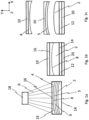
- a solid body 2 or a substrate is shown, which is arranged in the region of a radiation source 18, in particular a laser.
- the solid body 2 preferably has a first flat surface portion 14 and a second flat surface portion 16 , with the first flat surface portion 14 preferably being aligned essentially or exactly parallel to the second flat surface portion 16 .
- the first flat surface portion 14 and the second flat surface portion 16 preferably delimit the solid body 2 in a Y-direction, which is preferably aligned vertically or perpendicularly.
- the planar surface portions 14 and 16 preferably each extend in an XZ plane, with the XZ plane preferably being oriented horizontally. Alternatively, however, it is conceivable for the first and/or the second surface portion 14, 16 to have an uneven, in particular curved, shape.
- the radiation source 18 emits rays 6 onto the solid body 2 .
- the beams 6 penetrate to a defined depth into the solid body 2 and produce a crystal lattice modification 19, in particular a defect, at the respective position or at the respective predetermined position.
- so many modifications or crystal lattice modifications 19 are produced that at least one detachment region 8 is defined by them.
- the detachment area 8 has an uneven contour or uneven shape, with the detachment area 8 particularly preferably having a spherical shape, in particular a corrugated and/or arched and/or curved shape, at least in sections.
- the beams 6 can be guided through an optical system, for example for focusing or bundling, which is preferably arranged between the radiation source 18 and the solid body 2 (not shown).
- the reference number 9 designates a further detachment area in the solid body 2.
- the further detachment area 9 can also be produced during the production of the detachment area 8.
- the further detachment region 9 is preferably produced after the solid portion 4 has been separated or before the solid portion 4 has been separated.
- a plurality of solid body parts 4 , 5 are preferably defined by a plurality of detachment regions 8 , 9 in a solid body 2 , which can preferably be separated from the solid body 2 one after the other.
- exactly or at least one detachment region 8 is produced in a solid 2 .
- two, at least two or exactly two or three, at least three or exactly three or four, at least four or exactly four or five, at least five or exactly five or more, in particular e.g. up to 10 or 25 or 50 or 100 or 500, detachment areas are produced in the solid body 2.
- a multi-layer arrangement is shown, wherein the solid body 2 includes the detachment area 8 and is provided in the area of the first surface portion 14 with a holding layer 12, which in turn is preferably overlaid by a further layer 20, the further layer 20 preferably having a stabilization device, in particular a metal plate, is.
- An absorption layer, in particular a polymer layer 10 is preferably arranged on the second surface portion 16 of the solid body 2.
- the receiving layer 10 and/or the holding layer 12 preferably consist at least partially and particularly preferably completely of a polymer, in particular of PDMS.
- the recording layer 10 is produced on the surface of the solid body 2, for example by means of epitaxy.
- the recording layer 10 produced and the solid body 2 preferably have coefficients of thermal expansion that differ from one another.
- the receiving layer 10 which is also understood as a coating 50 in this case the multi-layer arrangement created preferably cools down, which results in stresses due to the different thermal expansion coefficients, as a result of which the solid portion 4 is separated or detached from the solid body 2 along the detachment region 8 .
- In 1c shows a state after crack initiation and subsequent crack development.
- the solid layer 4 adheres to the polymer layer 10 and is or can be spaced apart from the remainder of the solid body 2 .
- different detachment areas 8, 9 can have different shapes or contours. It is also conceivable that, for example, the second surface portion 16, which is a surface of the solid portion 4, 5 that is separated later, is brought into a different shape before the solid portion 4, 5 is separated. This change in shape can take place analogously to the separation of the solid portion 4, 5 or can be brought about by machining, in particular a grinding process.
- the present invention thus relates to a method for producing solid layers.
- the method according to the invention comprises at least the steps of providing a solid 2 for separating at least one solid layer 4, generating modifications, such as crystal lattice defects, by means of at least one laser, in particular at least one fs laser, in the internal structure of the solid to specify at least one Detachment region 8, 9, along which the solid layer / s 4, 5 is separated from the solid 2, are.
- the method according to the invention preferably comprises the step of thermally impinging on a polymer layer 10 arranged on the solid body 2 in order to generate, in particular mechanically, stresses in the solid body 2, with the stresses propagating a crack in the solid body 2 along the detachment region 8, which the solid layer 4 separates from the solid 2.
- FIG. 2a and 2b are examples of the in Fig. 1a shown generation of a detachment region 8 by the introduction of modifications 19, in particular defects or damaged areas, shown in a solid 2 by means of laser beams 6.
- FIG. 2a is thus shown schematically how modifications 19 can be produced in a solid body 2, in particular for producing a detachment region 8 by means of a radiation source 18, in particular one or more lasers, in particular one or more fs lasers.
- the radiation source 18 emits radiation 6 with a first wavelength 30 and a second wavelength 32.
- the wavelengths 30, 32 are included coordinated in such a way or the distance between the radiation source 18 and the detachment area 8 to be generated is adjusted in such a way that the waves 30, 32 meet essentially or exactly on the detachment area 8 in the solid body 2, whereby at the point of meeting 34 as a result of the energies both shafts 30, 32 a defect is generated.
- Defects can be generated by different or combined decomposition mechanisms, such as sublimation or chemical reactions, with the decomposition being able to be initiated thermally and/or photochemically, for example.
- a focused light beam 6 is shown, the focus of which is preferably in the detachment region 8 . It is conceivable here that the light beam 6 is focused by one or more focusing bodies, in particular lenses (not shown).
- FIG 3a an uneven solid portion 4 according to the invention or an uneven wafer is shown, wherein the solid portion 4 or the wafer 4 forms a warp according to one representation or shows a warp shape in cross section.
- the solid portion 4 it is conceivable here for the solid portion 4 to have two surface contours or surface shapes which are negative in relation to one another.
- the surface contours or surface shapes of the two opposing main surfaces 40, 42 of the solid portion 4 are not negative to one another, but rather have different contours or shapes.
- Figure 3b shows the production of a coating 50, in particular an epitaxially produced layer.
- the coating 50 is preferably arranged or produced on the solid portion 4 at a temperature of over 50° C., in particular over 100° C. or over 150° C. or over 200° C. or over 300° C. or over 400° C. It is conceivable here that the coating 50 is arranged or produced essentially or with a constant thickness on the solid portion 4 . Alternatively, however, it is also conceivable for the coating 50 to have locally different thicknesses.
- the further treatment thus represents the arrangement or production of a defined coating 50 on at least one surface 40, 42 of the solid portion 4.
- the specified parameters include at least data by which the thermal expansion coefficients of the material of the solid portion 4 and of the coating 50 are at least indirectly included or by which a deformation of the solid portion 4 as a result of a defined temperature control of the solid portion 4 provided with the coating 50 is included or specified.
- In 3c shows a situation after the production or arrangement of the coating 50 on at least one surface 40, 42 of the solid portion 4, the shape of the produced multi-component arrangement 39 having changed due to different thermal expansion coefficients.
- At least one of the main surfaces 40 and 44 of the multi-component arrangement 39 or multi-layer arrangement is preferably converted into a flat or essentially flat shape.
- the deformation preferably results from a preferably defined temperature control, in particular heating or cooling, of the multilayer arrangement 39.
- the solid portion 4 is thus designed according to the invention, depending on the subsequent treatment process, in particular the coating process, in such a way that the shape of one or both main surfaces 40, 42 of the solid portion 4 changes in a defined manner as a result of the treatment, in particular the coating process, in particular flattens out or is flat.
- the coating is particularly preferably a metal layer or a semiconductor layer, in particular a gallium nitride layer (GaN) or silicon layer, which is arranged or produced on a solid portion made of silicon, sapphire, silicon carbide (SiC) or gallium arsenide (GaAs).
Landscapes
- Engineering & Computer Science (AREA)
- Physics & Mathematics (AREA)
- Optics & Photonics (AREA)
- Mechanical Engineering (AREA)
- Plasma & Fusion (AREA)
- Microelectronics & Electronic Packaging (AREA)
- Manufacturing & Machinery (AREA)
- Computer Hardware Design (AREA)
- General Physics & Mathematics (AREA)
- Power Engineering (AREA)
- Condensed Matter Physics & Semiconductors (AREA)
- Mining & Mineral Resources (AREA)
- Chemical & Material Sciences (AREA)
- Chemical Kinetics & Catalysis (AREA)
- General Chemical & Material Sciences (AREA)
- Oil, Petroleum & Natural Gas (AREA)
- Crystals, And After-Treatments Of Crystals (AREA)
- Laser Beam Processing (AREA)
- Application Of Or Painting With Fluid Materials (AREA)
Description
Die vorliegende Erfindung bezieht sich gemäß Anspruch 1 auf ein Verfahren zum Abtrennen von mindestens einem Festkörperanteil von einem Festkörper Wafer sind in der Regel Festkörperteile, die von einem Festkörper abgetrennt wurden. Sie erstrecken sich im Wesentlichen zweidimensional, d.h. ihre Dicke ist gegenüber ihrer Breite und Länge um mindestens eine Größenordnung kleiner. Wafer werden bevorzugt in der Halbleitertechnik zur Herstellung von Solarzellen, Computerchips, LEDs, etc. verwendet. Die Erzeugung von Wafern ist sehr kostenintensiv, wodurch versucht wird möglichst viele Wafer aus einem Festkörper zu gewinnen. Dies führt dazu, dass die Wafer im dünner werden, was wiederum dazu führt, dass sie sich nach einer Beschichtung verformen, wenn die Temperaturausdehnungskoeffizienten der Beschichtung und des Wafers variieren. Eine solche Verformung wird als Warp bezeichnet, der eine Wölbung des Wafers beschreibt. Derartige Wölbungen werden z.B. durch die Druckschriften
Die
Die
Es ist die Aufgabe der vorliegenden Erfindung eine Lösung bereitzustellen, durch welche die zuvor genannten Mehrschichtanordnungen mit geringeren Warps oder ohne Warps hergestellt werden können.It is the object of the present invention to provide a solution by which the aforesaid multilayer arrangements can be produced with lower warps or without warps.
Die zuvor genannte Aufgabe wird erfindungsgemäß durch ein Verfahren nach Anspruch 1 gelöst.The aforementioned object is achieved according to the invention by a method according to claim 1.
Diese Lösung ist vorteilhaft, da der Festkörperanteil bevorzugt derart erzeugt wird, dass er infolge der späteren Bearbeitung die gewünschte Form annimmt. Es wird somit in Abhängigkeit der Materialeigenschaften des Festkörperanteils und der Beschichtung der Festkörperanteil mit einer Form erzeugt, durch welche die aus der Beschichtung resultierende Verformung ausgenutzt wird, um eine zumindest einerseits und bevorzugt beiderseits bevorzugt ebene oder im Wesentlichen ebene Oberfläche der Mehrschichtanordnung zu schaffen.This solution is advantageous because the solid portion is preferably produced in such a way that it assumes the desired shape as a result of subsequent processing. It is thus in Depending on the material properties of the solids portion and the coating, the solids portion is produced with a mold through which the deformation resulting from the coating is utilized in order to create a preferably flat or essentially flat surface of the multilayer arrangement at least on the one hand and preferably on both sides.
Weitere vorteilhafte Ausführungsformen sind Gegenstand der nachfolgenden Beschreibung und/oder der Unteransprüche.Further advantageous embodiments are the subject of the following description and/or the dependent claims.
Die Modifikationen werden gemäß der vorliegenden Erfindung innerhalb des Kristallgitters des Festkörpers mittels über eine äußere Oberfläche des Festkörperanteils in das Innere des Festkörperanteils eingeleitete Strahlung von mindestens einem Laser, insbesondere einem Piko- oder Femtosekunden-Laser, erzeugt. Zusätzlich ist denkbar, dass die Modifikationen in dem Kristallgitter durch Ionenimplantation erzeugt werden. Diese Ausführungsform ist vorteilhaft, da mittels Laserstrahlung und Ionenimplantation sehr genau Modifikationen erzeugt werden können. Der Ablösebereich kann somit sehr einfach in Abhängigkeit von den jeweiligen Parametern erzeugt werden.According to the present invention, the modifications are produced within the crystal lattice of the solid by means of radiation from at least one laser, in particular a picosecond or femtosecond laser, introduced via an outer surface of the solid portion into the interior of the solid portion. In addition, it is conceivable that the modifications in the crystal lattice are produced by ion implantation. This embodiment is advantageous since modifications can be produced very precisely by means of laser radiation and ion implantation. The detachment area can thus be generated very easily depending on the respective parameters.
Die einzelnen Modifikationen bzw. Defekte bzw. Schadstellen resultieren gemäß einer weiteren bevorzugten Ausführungsform der vorliegenden Erfindung jeweils aus einer von dem Laser, insbesondere einem Femtosekunden-Laser oder einem Pikosekunden-Laser, bewirkten multi-photonen Anregung. Bevorzugt hat der Laser eine Pulsdauer von unter 10ps, besonders bevorzugt unter 1ps und am höchsten bevorzugt von unter 500fs.According to a further preferred embodiment of the present invention, the individual modifications or defects or damaged areas result from multi-photon excitation brought about by the laser, in particular a femtosecond laser or a picosecond laser. The laser preferably has a pulse duration of less than 10 ps, particularly preferably less than 1 ps and most preferably less than 500 fs.
Gemäß einer weiteren bevorzugten Ausführungsform der vorliegenden Erfindung wird die Energie des Laserstrahls, insbesondere des fs-Lasers, derart gewählt, dass die Schädigungsausbreitung im Festkörper bzw. im Kristall kleiner als dreimal die Reyleighlänge, bevorzugt kleiner als die Reyleighlänge und besonders bevorzugt kleiner als ein Drittel der Reyleighlänge ist. Die Wellenlänge des Laserstrahls, insbesondere des fs-Lasers, wird gemäß einer weiteren bevorzugten Ausführungsform der vorliegenden Erfindung derart gewählt, dass die Absorption des Festkörpers bzw. des Materials kleiner als 10cm-1 und bevorzugt kleiner als 1cm-1 und besonders bevorzugt kleiner als 0,1cm-1 ist.According to a further preferred embodiment of the present invention, the energy of the laser beam, in particular of the fs laser, is selected in such a way that the damage propagation in the solid body or in the crystal is less than three times the Reyleigh length, preferably less than the Reyleigh length and particularly preferably less than one third is the Reyleigh length. According to a further preferred embodiment of the present invention, the wavelength of the laser beam, in particular of the fs laser, is selected in such a way that the absorption of the solid body or the material is less than 10 cm -1 and preferably less than 1 cm -1 and particularly preferably less than 0 .1 cm -1 .
Die weitere Behandlung umfasst gemäß vorliegenden Erfindung die Anordnung oder Erzeugung einer Beschichtung auf mindestens einer Oberfläche des Festkörperanteils. Die vorgegebenen Parameter umfassen dabei zumindest Daten, durch welche die thermischen Ausdehnungskoeffizienten des Materials des Festkörperanteils und der Beschichtung einbezogen werden. Zusätzlich umfassen die Parameter bevorzugt Daten, durch welche die Dicke/Höhe (bevorzugt durchschnittliche Dicke/Höhe) und/oder die Breite und/oder die Länge und/oder die Form des Festkörperanteils und/oder der Beschichtung einbezogen wird/werden. Diese Ausführungsform ist vorteilhaft, da dadurch sehr präzise für unterschiedliche Materialkombinationen (Festkörper und Beschichtung) Festkörperanteile erzeugt werden können.According to the present invention, the further treatment comprises the arrangement or production of a coating on at least one surface of the solid portion. In this case, the specified parameters include at least data by which the thermal expansion coefficients of the material of the solid portion and of the coating are included. In addition, the parameters preferably comprise data by which the thickness/height (preferably average thickness/height) and/or the width and/or the length and/or the shape of the solid fraction and/or the coating is/are included. This embodiment is advantageous because it allows solid parts to be produced very precisely for different material combinations (solid and coating).
Der Festkörper bzw. das Werkstück weist bevorzugt ein Material oder eine Materialkombination aus einer der Hauptgruppen 3, 4 und 5 des Periodensystems der Elemente auf, wie z.B. Si, SiC, SiGe, Ge, GaAs, InP, GaN, Al2O3 (Saphir), AIN. Besonders bevorzugt weist der Festkörper eine Kombination aus in der dritten und fünften Gruppe des Periodensystems vorkommenden Elementen auf. Denkbare Materialien oder Materialkombinationen sind dabei z.B. Galliumarsenid, Silizium, Siliziumcarbid, etc. Weiterhin kann der Festkörper eine Keramik (z.B. Al2O3 - Alumiumoxid) aufweisen oder aus einer Keramik bestehen, bevorzugte Keramiken sind dabei z.B. Perovskitkeramiken (wie z.B. Pb-, O-, Ti/Zr-haltige Keramiken) im Allgemeinen und Blei-Magnesium-Niobate, Bariumtitanat, Lithiumtitanat, Yttrium-Aluminium-Granat, insbesondere Yttrium-Aluminium-Granat Kristalle für Festkörperlaseranwendungen, SAW-Keramiken (surface acoustic wave), wie z.B. Lithiumniobat, Galliumorthophosphat, Quartz, Calziumtitanat, etc. im Speziellen. Der Festkörper weist somit bevorzugt ein Halbleitermaterial oder ein Keramikmaterial auf bzw. besonders bevorzugt besteht der Festkörper aus mindestens einem Halbleitermaterial oder einem Keramikmaterial. Es ist weiterhin denkbar, dass der Festkörper ein transparentes Material aufweist oder teilweise aus einem transparenten Material, wie z.B. Saphir, besteht bzw. gefertigt ist. Weitere Materialien, die hierbei als Festkörpermaterial alleine oder in Kombination mit einem anderen Material in Frage kommen, sind z.B. "wide band gap"-Materialien, InAISb, Hochtemperatursupraleiter, insbesondere seltene Erden Cuprate (z.B. YBa2Cu3O7). Es ist zusätzlich oder alternativ denkbar, dass der Festkörper eine Photomaske ist, wobei als Photomaskenmaterial im vorliegenden Fall bevorzugt jedes zum Anmeldetag bekannte Photomaskenmaterial und besonders bevorzugt Kombinationen daraus verwendet werden können.The solid or the workpiece preferably has a material or a material combination from one of the
Gemäß einer weiteren bevorzugten Ausführungsform der vorliegenden Erfindung wird mittels der Modifikationen mehr als 5%, insbesondere mehr als 10% oder mehr als 20% oder mehr als 30% oder mehr als 40% oder mehr als 50% oder mehr als 60% oder mehr als 70% oder mehr als 80% oder mehr als 90% oder mehr als 95%, des im Verlauf des Ablösebereichs ausgebildeten Kristallgitters verändert, insbesondere beschädigt. Diese Ausführungsform ist vorteilhaft, da z.B. durch die Laserbeaufschlagung das Kristallgitter derart verändert werden kann bzw. derart Defekte, insbesondere Mikrorisse, erzeugt werden können, dass die zum Abtrennen des Festkörperanteils von dem Festkörper erforderlichen Kräfte eingestellt werden können. Es ist somit im Sinne der vorliegenden Erfindung möglich, dass die Kristallstruktur im Ablösebereich derart mittels Laserstrahlung modifiziert bzw. beschädigt wird, dass sich der Festkörperanteil infolge der Laserbehandlung vom Festkörper ablöst bzw. abgetrennt wird.According to a further preferred embodiment of the present invention, by means of the modifications more than 5%, in particular more than 10% or more than 20% or more than 30% or more than 40% or more than 50% or more than 60% or more than 70% or more than 80% or more than 90% or more than 95% of the crystal lattice formed in the course of the detachment region is changed, in particular damaged. This embodiment is advantageous because the crystal lattice can be changed or defects, in particular microcracks, can be produced in such a way that the forces required to separate the solid portion from the solid can be set, e.g. by the laser impingement. It is therefore possible within the meaning of the present invention for the crystal structure in the detachment region to be modified or damaged by means of laser radiation in such a way that the solid portion detaches or is separated from the solid as a result of the laser treatment.
Das Ablösen des Festkörperanteils von dem Festkörper umfasst gemäß einer weiteren bevorzugten Ausführungsform der vorliegenden Erfindung zumindest die Schritte des Anordnens einer Aufnahmeschicht an dem Festkörper zum Halten des Festkörperanteils, und des thermischen Beaufschlagens der Aufnahmeschicht zum, insbesondere mechanischen, Erzeugen von Spannungen in dem Festkörper, wobei sich durch die Spannungen ein Riss in dem Festkörper entlang dem Ablösebereich ausbreitet, durch den der Festkörperanteil von dem Festkörper getrennt wird. Diese Ausführungsform ist vorteilhaft, da sehr genau und definiert Kräfte zum Abtrennen des Festkörperanteils von dem Festkörper erzeugbar sind.According to a further preferred embodiment of the present invention, the detachment of the solid portion from the solid body comprises at least the steps of arranging a receiving layer on the solid body to hold the solid portion, and subjecting the receiving layer to thermal stress to, in particular mechanically, generate stresses in the solid body, wherein the stresses propagate a crack in the solid along the detachment region, separating the solid portion from the solid. This embodiment is advantageous because forces for separating the solid portion from the solid can be generated very precisely and in a defined manner.
Gemäß einer weiteren bevorzugten Ausführungsform der vorliegenden Erfindung weist die Aufnahmeschicht ein Polymer, insbesondere PDMS, auf oder besteht daraus, wobei die thermische Beaufschlagung derart erfolgt, dass das Polymer einen Glasübergang erfährt.According to a further preferred embodiment of the present invention, the recording layer has or consists of a polymer, in particular PDMS, with the thermal loading taking place in such a way that the polymer undergoes a glass transition.
Die Aufnahmeschicht besteht bevorzugt aus Polydimethylsiloxane (PDMS) oder weist Polydimethylsiloxane (PDMS) auf.The receiving layer preferably consists of polydimethylsiloxane (PDMS) or has polydimethylsiloxane (PDMS).
Die thermische Beaufschlagung stellt bevorzugt ein Abkühlen der Aufnahmeschicht auf oder unter die Umgebungstemperatur und bevorzugt unter 10°C und besonders bevorzugt unter 0°C und weiter bevorzugt unter -10°C dar. Die Abkühlung der bevorzugt als Polymerschicht ausgebildeten Aufnahmeschicht erfolgt höchst bevorzugt derart, dass zumindest ein Teil der Aufnahmeschicht, die bevorzugt PDMS aufweist oder daraus besteht, einen Glasübergang vollzieht. Die Abkühlung kann hierbei eine Abkühlung auf unter -100°C sein, die z.B. mittels flüssigen Stickstoffs bewirkbar ist. Dies ist vorteilhaft, da sich die Aufnahmeschicht in Abhängigkeit von der Temperaturveränderung zusammenzieht, insbesondere einen Glasübergang erfährt, und die dabei entstehenden Kräfte auf den Festkörper überträgt, wodurch mechanische Spannungen in dem Festkörper erzeugbar sind, die zum Auslösen eines Risses und/oder zur Rissausbreitung führen.The thermal impact preferably represents a cooling of the recording layer to or below the ambient temperature and preferably below 10° C. and particularly preferably below 0° C. and more preferably below -10° C. The cooling of the recording layer, which is preferably designed as a polymer layer, is most preferably carried out in such a way that that at least part of the receiving layer, which preferably has PDMS or consists of it, undergoes a glass transition. In this case, the cooling can be cooling to below -100° C., which can be effected, for example, by means of liquid nitrogen. This is advantageous because the recording layer contracts depending on the temperature change, especially a Experiences glass transition, and the resulting forces are transmitted to the solid body, whereby mechanical stresses can be generated in the solid body, which lead to the initiation of a crack and / or crack propagation.
Die Aufgabe wird ferner durch ein Verfahren zur Herstellung einer Mehrschichtanordnung gelöst. Das Verfahren zur Herstellung der Mehrschichtanordnung umfasst dabei mindestens die Schritte: Bereitstellen eines, insbesondere gewölbten, Wafers mit einer ersten unebenen Form; Anordnen oder Erzeugen einer weiteren Schicht an mindestens einer Oberfläche des Wafers; wobei die weitere Schicht und der Wafer unterschiedliche thermische Ausdehnungskoeffizienten aufweisen, wobei die weitere Schicht bei einer von einer Zieltemperatur verschiedenen Beschichtungstemperatur an der Oberfläche des Wafers angeordnet oder daran erzeugt wird, und wobei die weitere Schicht derart ausgestaltet ist, dass sie den Wafer beim Erreichen der Zieltemperatur derart beaufschlagt, dass der Wafer aus der ersten unebenen Form in eine zweite Form, die von der ersten Form abweicht, verformt wird, wobei die zweite Form bevorzugt eine ebene Form darstellt. Bevorzugt weist der unebene Festkörper einen Warp auf bzw. bildet einen Warp aus, der negativ oder im Wesentlichen negativ zu der durch die Beschichtung bewirkte Verformung des Festkörperanteils ist.The object is also achieved by a method for producing a multilayer arrangement. The method for producing the multilayer arrangement comprises at least the following steps: providing a wafer, in particular a curved one, with a first uneven shape; arranging or creating a further layer on at least one surface of the wafer; wherein the further layer and the wafer have different coefficients of thermal expansion, wherein the further layer is arranged or produced on the surface of the wafer at a coating temperature that differs from a target temperature, and wherein the further layer is designed in such a way that it breaks the wafer when the Target temperature applied in such a way that the wafer is deformed from the first uneven shape into a second shape that deviates from the first shape, the second shape preferably being a flat shape. The uneven solid preferably has a warp or forms a warp which is negative or essentially negative in relation to the deformation of the solid portion caused by the coating.
Diese Lösung ist vorteilhaft, da durch die definierte Gestaltung des Wafers vorteilhaft die infolge der Beschichtung auftretende Verformung ausgenutzt wird, um eine bevorzugt zumindest einerseits bevorzugt ebene Mehrschichtanordnung zu erhalten. Besonders bevorzugt wird die weitere Schicht mittels Epitaxie erzeugt.This solution is advantageous because the defined design of the wafer advantageously utilizes the deformation occurring as a result of the coating in order to obtain a multilayer arrangement that is preferably planar at least on the one hand. The further layer is particularly preferably produced by means of epitaxy.
Zusätzlich ist denkbar, dass der Wafer vor dem Anordnen oder Erzeugen der weiteren Schicht bereits mit einer Beschichtung versehen wurde.In addition, it is conceivable that the wafer has already been provided with a coating before the further layer is arranged or produced.
Weiterhin bezieht sich die vorliegende Erfindung ebenfalls auf einen unebenen Festkörperanteil, insbesondere auf einen unebenen, insbesondere gewölbten, Wafer. Der unebene, insbesondere gewölbte, Festkörperanteil ist dabei bevorzugt nach einem Verfahren hergestellt, dass mindestens die nachfolgend genannten Schritte umfasst:
Bereitstellen eines Festkörpers zum Abtrennen des unebenen Festkörperanteils, Modifizieren des Kristallgitters des Festkörpers mittels eines Modifikationsmittels, insbesondere eines Lasers, insbesondere eines Piko- oder Femtosekunden-Laser, wobei mehrere Modifikationen zum Ausbilden eines unebenen Ablösebereichs in dem Kristallgitter erzeugt werden, wobei die Modifikationen in Abhängigkeit von vorgegebenen Parametern erzeugt werden, wobei die vorgegebenen Parameter einen Zusammenhang zwischen einer Verformung des Festkörperanteils in Abhängigkeit von einer definierten weiteren Behandlung des Festkörperanteils beschreiben, Ablösen des Festkörperanteils von dem Festkörper.Furthermore, the present invention also relates to an uneven solid portion, in particular to an uneven, in particular curved, wafer. The uneven, in particular curved, solid portion is preferably produced by a method that includes at least the following steps:
Providing a solid for separating the uneven solid part, modifying the crystal lattice of the solid by means of a modifier, in particular a laser, in particular a picosecond or femtosecond laser, with several modifications to form an uneven detachment area in the crystal lattice being generated, the modifications being dependent are generated by predetermined parameters, the predetermined parameters have a connection between a Describe deformation of the solid portion as a function of a defined further treatment of the solid portion, detachment of the solid portion from the solid.
Weiterhin bezieht sich die vorliegende Erfindung besonders bevorzugt auf eine Mehrschichtanordnung. Die erfindungsgemäße Mehrschichtanordnung weist bevorzugt mindestens einen Festkörperanteil, insbesondere einen Wafer, auf, wobei der Festkörperanteil nach einem Verfahren gemäß einem der Ansprüche 1 bis 4 hergestellt ist und zunächst mindestens eine unebene Oberfläche aufweist. Weiterhin weist die Mehrschichtanordnung mindestens eine an dem Festkörperanteil angeordnete oder erzeugte Beschichtung auf, wobei die Beschichtung bei einer von einer Zieltemperatur verschiedenen Beschichtungstemperatur an dem Festkörperanteil angeordnet oder erzeugt wurde, wobei der Festkörperanteil eine Verformungsoberfläche mit einer zunächst unebenen ersten Oberflächenform aufweist, wobei der Temperaturausdehnungskoeffizient des Materials des Festkörperanteils und der Temperaturausdehnungskoeffizient des Materials der Beschichtung voneinander verschieden sind, wobei die Verformungsoberfläche des beschichteten Festkörperanteils bei der Zieltemperatur eine zweite Oberflächenform ausbildet, wobei die zweite Oberflächenform und die erste Oberflächenform voneinander verschieden sind.Furthermore, the present invention particularly preferably relates to a multilayer arrangement. The multilayer arrangement according to the invention preferably has at least one solid portion, in particular a wafer, wherein the solid portion is produced by a method according to one of claims 1 to 4 and initially has at least one uneven surface. Furthermore, the multi-layer arrangement has at least one coating arranged or produced on the solid portion, the coating being arranged or produced on the solid portion at a coating temperature that differs from a target temperature, the solid portion having a deformation surface with an initially uneven first surface shape, the temperature expansion coefficient of the Material of the solid portion and the temperature expansion coefficient of the material of the coating are different from each other, wherein the deformation surface of the coated solid portion forms a second surface shape at the target temperature, the second surface shape and the first surface shape are different from each other.
Die Verwendung der Wörter "im Wesentlichen" definiert bevorzugt in allen Fällen, in denen diese Wörter im Rahmen der vorliegenden Erfindung verwendet werden eine Abweichung im Bereich von 1%-30%, insbesondere von 1%-20%, insbesondere von 1%-10%, insbesondere von 1%-5%, insbesondere von 1%-2%, von der Festlegung, die ohne die Verwendung dieser Wörter gegeben wäre.The use of the words “substantially” preferably defines a deviation in the range of 1%-30%, in particular 1%-20%, in particular 1%-10 in all cases in which these words are used within the scope of the present invention %, in particular from 1%-5%, in particular from 1%-2%, from the determination that would have been given without the use of these words.
Weitere Vorteile, Ziele und Eigenschaften der vorliegenden Erfindung werden anhand nachfolgender Beschreibung anliegender Zeichnungen erläutert, in welchen beispielhaft die erfindungsgemäße Festkörperherstellung oder Waferherstellung dargestellt ist. Bauteile oder Elemente der erfindungsgemäßen Festkörperherstellung oder Waferherstellung, welche in den Figuren wenigstens im Wesentlichen hinsichtlich ihrer Funktion übereinstimmen, können hierbei mit gleichen Bezugszeichen gekennzeichnet sein, wobei diese Bauteile oder Elemente nicht in allen Figuren beziffert oder erläutert sein müssen.Further advantages, goals and properties of the present invention are explained with reference to the following description of the attached drawings, in which the solid body production or wafer production according to the invention is shown by way of example. Components or elements of the solid body production or wafer production according to the invention, which correspond in the figures at least essentially with regard to their function, can be identified with the same reference symbols, whereby these components or elements do not have to be numbered or explained in all figures.
Darin zeigen:
- Fig. 1a
- einen schematischen Aufbau zum Erzeugen von Defekten in einem Festkörper;
- Fig. 1b
- eine schematische Darstellung einer Schichtanordnung vor dem Abtrennen einer Festkörperschicht von einem Festkörper;
- Fig. 1c
- eine schematische Darstellung einer Schichtanordnung nach dem Abtrennen einer Festkörperschicht von einem Festkörper;
- Fig. 2a
- eine erste schematisch dargestellte Variante zur Defekterzeugung mittels Laserstrahlung;
- Fig. 2b
- eine zweite schematisch dargestellte Variante zur Defekterzeugung mittels Laserstrahung;
- Fig. 3a
- eine schematische Seitenansicht eines erfindungsgemäßen unebenen Wafers;
- Fig. 3b
- eine schematische Seitenansicht eines erfindungsgemäßen unebenen Wafers mit einer daran angeordneten oder erzeugten Beschichtung; und
- Fig. 3c
- eine schematische Seitenansicht einer bevorzugten Form einer erfindungsgemäßen Mehrschichtanordnung nach einer definierten Temperierung.
- Fig. 1a
- a schematic structure for generating defects in a solid;
- Fig. 1b
- a schematic representation of a layer arrangement before the separation of a solid layer from a solid;
- 1c
- a schematic representation of a layer arrangement after the separation of a solid layer from a solid;
- Figure 2a
- a first schematically illustrated variant for generating defects by means of laser radiation;
- Figure 2b
- a second schematically illustrated variant for generating defects by means of laser radiation;
- Figure 3a
- a schematic side view of an uneven wafer according to the invention;
- Figure 3b
- a schematic side view of an uneven wafer according to the invention with a coating arranged or produced thereon; and
- 3c
- a schematic side view of a preferred form of a multilayer arrangement according to the invention after a defined temperature control.
In
Weiterhin lässt sich dieser Darstellung entnehmen, dass die Strahlungsquelle 18 Stahlen 6 auf den Festkörper 2 ausstrahlt. Die Strahlen 6 dringen je nach Konfiguration bzw. in Abhängigkeit von vorgegebenen Parametern definiert tief in den Festkörper 2 ein und erzeugen an der jeweiligen Position bzw. an der jeweils vorbestimmten Position eine Kristallgittermodifikation 19, insbesondere einen Defekt. Bevorzugt werden so viele Modifikationen bzw. Kristallgittermodifikationen 19 erzeugt, dass durch diese mindestens ein Ablösebereich 8 vorgegeben wird. Der Ablösebereich 8 weist eine unebene Kontur bzw. unebene Form auf, wobei der Ablösebereich 8 besonders bevorzugt zumindest abschnittsweise eine sphärische, insbesondere gewellte und/oder gewölbte und/oder gebogene, Form aufweist. Weiterhin können die Strahlen 6 z.B. zum Fokussieren oder Bündeln durch eine Optik geleitet werden, die bevorzugt zwischen der Strahlungsquelle 18 und dem Festkörper 2 angeordnet ist (nicht gezeigt).Furthermore, it can be seen from this representation that the
Das Bezugszeichen 9 kennzeichnet einen weiteren Ablösebereich in dem Festkörper 2. Gemäß der vorliegenden Erfindung kann der weitere Ablösebereich 9 ebenfalls während der Erzeugung des Ablösebereichs 8 erzeugt werden. Alternativ ist denkbar, dass der weitere Ablösebereich 9 nach oder vor der Erzeugung des Ablösebereichs 8 erzeugt wird. Bevorzugt wird der weitere Ablösebereich 9 nach dem Abtrennen des Festkörperanteils 4 oder vor dem Abtrennen des Festkörperanteils 4 erzeugt. Bevorzugt werden durch mehrere Ablösebereiche 8, 9 in einem Festkörper 2 mehrere Festkörperanteile 4, 5 definiert, die bevorzugt nacheinander von dem Festkörper 2 abtrennbar sind. Gemäß einer bevorzugten Ausführungsform der vorliegenden Erfindung wird in einem Festkörper 2 genau oder mindestens ein Ablösebereich 8 erzeugt. Gemäß einer weiteren bevorzugten Ausführungsform der vorliegenden Erfindung werden zwei, mindestens zwei oder genau zwei oder drei, mindestens drei oder genau drei oder vier, mindestens vier oder genau vier oder fünf, mindestens fünf oder genau fünf oder mehrere, insbesondere z.B. bis zu 10 oder 25 oder 50 oder 100 oder 500, Ablösebereiche in dem Festkörper 2 erzeugt.The
In
In
Weiterhin können gemäß der vorliegenden Erfindung unterschiedliche Ablösebereiche 8, 9 unterschiedliche Formen bzw. Konturen aufweisen. Weiterhin ist denkbar, dass z.B. der zweite Flächenanteil 16, der eine Oberfläche des später abgetrennten Festkörperanteils 4, 5 ist, vor dem Abtrennen des Festkörperanteils 4, 5 in eine andere Form gebracht wird. Diese Formänderung kann analog zum Abtrennen des Festkörperanteils 4, 5 erfolgen oder durch eine spanende Bearbeitung, insbesondere einen Schleifprozess, bewirkt werden.Furthermore, according to the present invention,
Die vorliegende Erfindung bezieht sich somit auf ein Verfahren zum Herstellen von Festkörperschichten. Das erfindungsgemäße Verfahren umfasst dabei mindestens die Schritte des Bereitstellens eines Festkörpers 2 zum Abtrennen mindestens einer Festkörperschicht 4, des Erzeugens von Modifikationen, wie Kristallgitterdefekten, mittels mindestens einem Laser, insbesondere mindestens einem fs-Laser, in der inneren Struktur des Festkörpers zum Vorgeben mindestens eines Ablösebereichs 8, 9, entlang dem die Festkörperschicht/en 4, 5 vom Festkörper 2 abgetrennt wird, werden. Ferner umfasst das erfindungsgemäße Verfahren bevorzugt den Schritt des thermischen Beaufschlagens einer an dem Festkörper 2 angeordneten Polymerschicht 10 zum, insbesondere mechanischen, Erzeugen von Spannungen in dem Festkörper 2, wobei sich durch die Spannungen ein Riss in dem Festkörper 2 entlang des Ablösebereichs 8 ausbreitet, der die Festkörperschicht 4 von dem Festkörper 2 abtrennt.The present invention thus relates to a method for producing solid layers. The method according to the invention comprises at least the steps of providing a solid 2 for separating at least one
In den
In
In
In
In
Der Festkörperanteil 4 ist somit erfindungsgemäß derart in Abhängigkeit von dem nachgelagerten Behandlungsverfahren, insbesondere Beschichtungsverfahren, gestaltet, dass sich die Form einer oder beider Hauptoberflächen 40, 42 des Festkörperanteils 4 infolge der Behandlung, insbesondere des Beschichtungsverfahrens, definiert verändert, insbesondere abflacht oder eben ausbildet. Besonders bevorzugt handelt es sich bei der Beschichtung um eine Metallschicht oder eine Halbleiterschicht, insbesondere um eine Galliumnitridschicht (GaN) oder Siliziumschicht, die auf einem Festkörperanteil aus Silizium, Saphir, Siliziumcarbid (SiC) oder Galliumarsenid (GaAs) angeordnet oder erzeugt wird.The
- 22
- Festkörpersolid
- 44
- Festkörperanteilsolid content
- 55
- weiterer Festkörperanteiladditional solids
- 66
- Strahlungradiation
- 88th
- Ablösebereichrelease area
- 99
- weiterer Ablösebereichfurther detachment area
- 1010
- Aufnahmeschichtrecording layer
- 1212
- Halteschichtholding layer
- 1414
- erster Flächenanteilfirst area share
- 1616
- zweiter Flächenanteilsecond area share
- 1818
- Strahlungsquelleradiation source
- 1919
- Modifikationmodification
- 2020
- Stabilisierungseinrichtungstabilization device
- 3030
- erster Strahlungsanteilfirst portion of radiation
- 3232
- zweiter Strahlungsanteilsecond portion of radiation
- 3434
- Ort der Defekterzeugunglocation of defect generation
- 4040
- erste Hauptoberfläche des Festkörperanteilsfirst major surface of the solid portion
- 4242
- zweite Hauptoberfläche des Festkörperanteilssecond major surface of the solid portion
- 4444
- zweite Hauptoberfläche der Mehrkomponentenanordnungsecond major surface of the multi-component arrangement
- 5050
- Beschichtungcoating
- XX
- erste Richtungfirst direction
- YY
- zweite Richtungsecond direction
- ZZ
- dritte Richtungthird direction
Claims (4)
- Method for separating at least one solid-state component (4), in particular a wafer, from a solid-state body (2), at least comprising the steps of:modifying the crystal lattice of the solid-state body (2) by means of a modification means (18), wherein a plurality of modifications (19) are generated so as to form a non-planar, in particular curved, detachment region (8) in the interior of the solid-state body (2),detaching the solid-state component (4) from the solid-state body (2) along the detachment region, andfurther treating the solid-state component (4) in a defined manner, leading to a deformation of the solid-state component (4),wherein the positions of the modifications (19) are generated in dependence on predefined parameters which describe a relationship between the deformation of the solid-state component (4) in dependence on the defined further treatment of the solid-state component (4),wherein the modifications (19) within the crystal lattice of the solid-state body (2) are generated by means of radiation (6) from at least one laser, in particular a picosecond or femtosecond laser, introduced via an outer surface of the solid-state component (4) into the interior of the solid-state component (4),wherein further treatment of the solid-state component comprises the arrangement or generation of a defined coating (50) on at least one surface (40, 42) of the solid-state component (4), andcharacterized in that
the predefined parameters at least comprise data which include, at least indirectly, the thermal expansion coefficients of the material of the solid-state component (4) and of the coating (50) or which include or predefine a deformation of the solid-state component (4) as a result of a defined temperature control of the solid-state component (4) provided with the coating (50). - Method according to one of the preceding claims,
wherein more than 5%, in particular more than 10% or more than 20% or more than 50% or more than 80%, of the crystal lattice formed in the profile of the detachment region (8) is changed, in particular damaged, by the modifications (19). - Method according to Claim 1 or 2,
wherein the detachment of the solid-state component (4) from the solid-state body (2) comprises at least the following steps:arranging a receiving layer (10) on the solid-state body (2) for holding of the solid-state component (4), andsubjecting the receiving layer (10) to thermal stress for, in particular mechanical, generation of stresses in the solid-state body (2),wherein, as a result of the stresses, a crack in the solid-state body (2) propagates along the detachment region (8), by means of which the solid-state component (4) is separated from the solid-state body (2). - Method according to Claim 3,wherein the receiving layer (10) comprises or consists of a polymer, in particular PDMS, andwherein the thermal stress is effected in such a way that the polymer undergoes a glass transition.
Priority Applications (1)
| Application Number | Priority Date | Filing Date | Title |
|---|---|---|---|
| EP23167033.2A EP4224513A1 (en) | 2015-01-15 | 2016-01-13 | Non-planar wafer and method for producing a non-planar wafer |
Applications Claiming Priority (2)
| Application Number | Priority Date | Filing Date | Title |
|---|---|---|---|
| DE102015000451.4A DE102015000451A1 (en) | 2015-01-15 | 2015-01-15 | Uneven Wafer and Method of Making an Uneven Wafer |
| PCT/EP2016/050574 WO2016113309A1 (en) | 2015-01-15 | 2016-01-13 | Nonplanar wafer and method for producing a nonplanar wafer |
Related Child Applications (2)
| Application Number | Title | Priority Date | Filing Date |
|---|---|---|---|
| EP23167033.2A Division EP4224513A1 (en) | 2015-01-15 | 2016-01-13 | Non-planar wafer and method for producing a non-planar wafer |
| EP23167033.2A Division-Into EP4224513A1 (en) | 2015-01-15 | 2016-01-13 | Non-planar wafer and method for producing a non-planar wafer |
Publications (2)
| Publication Number | Publication Date |
|---|---|
| EP3245665A1 EP3245665A1 (en) | 2017-11-22 |
| EP3245665B1 true EP3245665B1 (en) | 2023-07-05 |
Family
ID=55129872
Family Applications (2)
| Application Number | Title | Priority Date | Filing Date |
|---|---|---|---|
| EP16700464.7A Active EP3245665B1 (en) | 2015-01-15 | 2016-01-13 | Method for producing a nonplanar wafer |
| EP23167033.2A Pending EP4224513A1 (en) | 2015-01-15 | 2016-01-13 | Non-planar wafer and method for producing a non-planar wafer |
Family Applications After (1)
| Application Number | Title | Priority Date | Filing Date |
|---|---|---|---|
| EP23167033.2A Pending EP4224513A1 (en) | 2015-01-15 | 2016-01-13 | Non-planar wafer and method for producing a non-planar wafer |
Country Status (5)
| Country | Link |
|---|---|
| US (1) | US11786995B2 (en) |
| EP (2) | EP3245665B1 (en) |
| CN (1) | CN107206626B (en) |
| DE (1) | DE102015000451A1 (en) |
| WO (1) | WO2016113309A1 (en) |
Families Citing this family (6)
| Publication number | Priority date | Publication date | Assignee | Title |
|---|---|---|---|---|
| DE102015006971A1 (en) | 2015-04-09 | 2016-10-13 | Siltectra Gmbh | Method for producing low-loss multi-component wafers |
| WO2017167614A1 (en) * | 2016-03-22 | 2017-10-05 | Siltectra Gmbh | Combined laser treatment of a solid body to be split |
| DE102017010284A1 (en) * | 2017-11-07 | 2019-05-09 | Siltectra Gmbh | Method of thinning component-coated solid layers |
| DE102018003675A1 (en) * | 2018-05-04 | 2019-11-07 | Siltectra Gmbh | Method for separating solid layers of composite structures from SiC and a metallic coating or electrical components |
| DE102018111793A1 (en) | 2018-05-16 | 2019-11-21 | Schmitt Prof. Möhlmann & Collegen Wirtschaftskanzlei-Insolvenzverwalter Aktiengesellschaft | gas bottle |
| KR102178626B1 (en) * | 2018-10-30 | 2020-11-16 | 에이피시스템 주식회사 | Method of Peeling Lamination Structure, Method of Repairing Organic Light Emitting Device and Apparatus of Peeling Lamination Structure |
Citations (2)
| Publication number | Priority date | Publication date | Assignee | Title |
|---|---|---|---|---|
| US20140038392A1 (en) * | 2012-02-26 | 2014-02-06 | Solexel, Inc. | Systems and methods for laser splitting and device layer transfer |
| EP3137657A1 (en) * | 2014-04-30 | 2017-03-08 | Siltectra GmbH | Combined method for producing solids, involving laser treatment and temperature-induced stresses to generate three-dimensional solids |
Family Cites Families (23)
| Publication number | Priority date | Publication date | Assignee | Title |
|---|---|---|---|---|
| US3808674A (en) * | 1972-08-10 | 1974-05-07 | Westinghouse Electric Corp | Epitaxial growth of thermically expandable films and particularly anisotropic ferro-electric films |
| US6156623A (en) | 1998-03-03 | 2000-12-05 | Advanced Technology Materials, Inc. | Stress control of thin films by mechanical deformation of wafer substrate |
| TW417315B (en) | 1998-06-18 | 2001-01-01 | Sumitomo Electric Industries | GaN single crystal substrate and its manufacture method of the same |
| KR100304664B1 (en) | 1999-02-05 | 2001-09-26 | 윤종용 | Method for fabricating a GaN film |
| JP2003063897A (en) | 2001-08-28 | 2003-03-05 | Sony Corp | Nitride-based iii-v group compound semiconductor substrate and method for producing the same, method for producing light emitting device of semiconductor and method for producing semiconductor device |
| KR101094403B1 (en) | 2004-01-29 | 2011-12-15 | 삼성코닝정밀소재 주식회사 | Sapphire/gallium nitride laminate having reduced bending deformation |
| KR100631905B1 (en) | 2005-02-22 | 2006-10-11 | 삼성전기주식회사 | Nitride single crystal substrate manufacturing method and nitride semiconductor light emitting device manufacturing method using the same |
| US7592629B2 (en) | 2005-07-18 | 2009-09-22 | Samsung Corning Co., Ltd. | Gallium nitride thin film on sapphire substrate having reduced bending deformation |
| US8749020B2 (en) * | 2007-03-09 | 2014-06-10 | Taiwan Semiconductor Manufacturing Company, Ltd. | Metal e-fuse structure design |
| JP2009061462A (en) * | 2007-09-05 | 2009-03-26 | Sumitomo Electric Ind Ltd | Method for manufacturing substrate, and substrate |
| TWI466749B (en) * | 2007-11-02 | 2015-01-01 | Mitsuboshi Diamond Ind Co Ltd | Method for Segmentation of Fragile Material Substrate |
| US20100264518A1 (en) * | 2009-04-15 | 2010-10-21 | Lee Shura | Wafer and method for construction, strengthening and homogenization thereof |
| US8278187B2 (en) | 2009-06-24 | 2012-10-02 | Semiconductor Energy Laboratory Co., Ltd. | Method for reprocessing semiconductor substrate by stepwise etching with at least two etching treatments |
| DE102010030358B4 (en) * | 2010-06-22 | 2014-05-22 | Osram Opto Semiconductors Gmbh | Method for separating a substrate wafer |
| JP5508533B2 (en) * | 2010-07-26 | 2014-06-04 | 浜松ホトニクス株式会社 | Manufacturing method of light absorbing substrate and manufacturing method of mold for manufacturing the same |
| US20130312460A1 (en) * | 2011-02-10 | 2013-11-28 | National University Corporation Saitama University | Manufacturing method of single crystal substrate and manufacturing method of internal modified layer-forming single crystal member |
| US20130316538A1 (en) * | 2012-05-23 | 2013-11-28 | International Business Machines Corporation | Surface morphology generation and transfer by spalling |
| KR102061695B1 (en) * | 2012-10-17 | 2020-01-02 | 삼성전자주식회사 | Wafer processing method |
| KR102077248B1 (en) * | 2013-01-25 | 2020-02-13 | 삼성전자주식회사 | Methods for processing substrates |
| DE102013007671A1 (en) * | 2013-05-03 | 2014-11-06 | Siltectra Gmbh | Process for producing a wafer with carrier unit |
| WO2015010706A1 (en) * | 2013-07-23 | 2015-01-29 | Fraunhofer-Gesellschaft zur Förderung der angewandten Forschung e.V. | Method and device for separating a flat workpiece into multiple parts |
| TWI657480B (en) * | 2014-06-25 | 2019-04-21 | 環球晶圓股份有限公司 | Silicon substrates with compressive stress and methods for production of the same |
| US10611052B1 (en) * | 2019-05-17 | 2020-04-07 | Cree, Inc. | Silicon carbide wafers with relaxed positive bow and related methods |
-
2015
- 2015-01-15 DE DE102015000451.4A patent/DE102015000451A1/en active Pending
-
2016
- 2016-01-13 EP EP16700464.7A patent/EP3245665B1/en active Active
- 2016-01-13 EP EP23167033.2A patent/EP4224513A1/en active Pending
- 2016-01-13 CN CN201680005975.0A patent/CN107206626B/en active Active
- 2016-01-13 WO PCT/EP2016/050574 patent/WO2016113309A1/en active Application Filing
- 2016-01-13 US US15/543,878 patent/US11786995B2/en active Active
Patent Citations (2)
| Publication number | Priority date | Publication date | Assignee | Title |
|---|---|---|---|---|
| US20140038392A1 (en) * | 2012-02-26 | 2014-02-06 | Solexel, Inc. | Systems and methods for laser splitting and device layer transfer |
| EP3137657A1 (en) * | 2014-04-30 | 2017-03-08 | Siltectra GmbH | Combined method for producing solids, involving laser treatment and temperature-induced stresses to generate three-dimensional solids |
Also Published As
| Publication number | Publication date |
|---|---|
| EP4224513A1 (en) | 2023-08-09 |
| CN107206626A (en) | 2017-09-26 |
| US20180001416A1 (en) | 2018-01-04 |
| DE102015000451A1 (en) | 2016-07-21 |
| US11786995B2 (en) | 2023-10-17 |
| WO2016113309A1 (en) | 2016-07-21 |
| CN107206626B (en) | 2019-08-20 |
| EP3245665A1 (en) | 2017-11-22 |
Similar Documents
| Publication | Publication Date | Title |
|---|---|---|
| EP3245665B1 (en) | Method for producing a nonplanar wafer | |
| EP3666445B1 (en) | Solid body division by conversion of substances | |
| EP3055098B1 (en) | Wafer production method | |
| EP3280577B1 (en) | Method for the material-saving production of wafers | |
| EP3253529B1 (en) | Separation of a solid body by material modification | |
| EP3055447B1 (en) | Creation of a crack-initiating point or a cracking line for the improved splitting off of a solid layer from a solid body | |
| DE102014002600A1 (en) | Combined wafer fabrication process with laser treatment and temperature-induced stresses | |
| DE102015004603A1 (en) | Combined wafer fabrication process with laser treatment and temperature-induced stresses | |
| EP3137657B1 (en) | Combined method for producing solids, involving laser treatment and temperature-induced stresses to generate three-dimensional solids | |
| EP2859985B1 (en) | Wafer production method | |
| WO2016055443A1 (en) | Splitting method and use of a material in a splitting method | |
| EP3201941B1 (en) | Combined wafer production method with a receiving layer having holes | |
| EP3055099A1 (en) | Method for manufacturing solid state elements by a laser treatment and temperature-induced stresses |
Legal Events
| Date | Code | Title | Description |
|---|---|---|---|
| STAA | Information on the status of an ep patent application or granted ep patent |
Free format text: STATUS: THE INTERNATIONAL PUBLICATION HAS BEEN MADE |
|
| PUAI | Public reference made under article 153(3) epc to a published international application that has entered the european phase |
Free format text: ORIGINAL CODE: 0009012 |
|
| STAA | Information on the status of an ep patent application or granted ep patent |
Free format text: STATUS: REQUEST FOR EXAMINATION WAS MADE |
|
| 17P | Request for examination filed |
Effective date: 20170816 |
|
| AK | Designated contracting states |
Kind code of ref document: A1 Designated state(s): AL AT BE BG CH CY CZ DE DK EE ES FI FR GB GR HR HU IE IS IT LI LT LU LV MC MK MT NL NO PL PT RO RS SE SI SK SM TR |
|
| AX | Request for extension of the european patent |
Extension state: BA ME |
|
| RAP1 | Party data changed (applicant data changed or rights of an application transferred) |
Owner name: SILTECTRA GMBH |
|
| DAV | Request for validation of the european patent (deleted) | ||
| DAX | Request for extension of the european patent (deleted) | ||
| STAA | Information on the status of an ep patent application or granted ep patent |
Free format text: STATUS: EXAMINATION IS IN PROGRESS |
|
| 17Q | First examination report despatched |
Effective date: 20210216 |
|
| STAA | Information on the status of an ep patent application or granted ep patent |
Free format text: STATUS: EXAMINATION IS IN PROGRESS |
|
| GRAP | Despatch of communication of intention to grant a patent |
Free format text: ORIGINAL CODE: EPIDOSNIGR1 |
|
| RIC1 | Information provided on ipc code assigned before grant |
Ipc: B23K 103/00 20060101ALN20221222BHEP Ipc: B28D 1/22 20060101ALI20221222BHEP Ipc: B23K 26/53 20140101ALI20221222BHEP Ipc: B23K 26/0622 20140101ALI20221222BHEP Ipc: B28D 5/00 20060101ALI20221222BHEP Ipc: H01L 21/02 20060101AFI20221222BHEP |
|
| STAA | Information on the status of an ep patent application or granted ep patent |
Free format text: STATUS: GRANT OF PATENT IS INTENDED |
|
| INTG | Intention to grant announced |
Effective date: 20230126 |
|
| GRAS | Grant fee paid |
Free format text: ORIGINAL CODE: EPIDOSNIGR3 |
|
| GRAA | (expected) grant |
Free format text: ORIGINAL CODE: 0009210 |
|
| STAA | Information on the status of an ep patent application or granted ep patent |
Free format text: STATUS: THE PATENT HAS BEEN GRANTED |
|
| AK | Designated contracting states |
Kind code of ref document: B1 Designated state(s): AL AT BE BG CH CY CZ DE DK EE ES FI FR GB GR HR HU IE IS IT LI LT LU LV MC MK MT NL NO PL PT RO RS SE SI SK SM TR |
|
| REG | Reference to a national code |
Ref country code: CH Ref legal event code: EP |
|
| REG | Reference to a national code |
Ref country code: AT Ref legal event code: REF Ref document number: 1585627 Country of ref document: AT Kind code of ref document: T Effective date: 20230715 |
|
| REG | Reference to a national code |
Ref country code: DE Ref legal event code: R096 Ref document number: 502016015912 Country of ref document: DE |
|
| REG | Reference to a national code |
Ref country code: IE Ref legal event code: FG4D Free format text: LANGUAGE OF EP DOCUMENT: GERMAN |
|
| REG | Reference to a national code |
Ref country code: LT Ref legal event code: MG9D |
|
| REG | Reference to a national code |
Ref country code: NL Ref legal event code: MP Effective date: 20230705 |
|
| P01 | Opt-out of the competence of the unified patent court (upc) registered |
Effective date: 20231020 |
|
| PG25 | Lapsed in a contracting state [announced via postgrant information from national office to epo] |
Ref country code: NL Free format text: LAPSE BECAUSE OF FAILURE TO SUBMIT A TRANSLATION OF THE DESCRIPTION OR TO PAY THE FEE WITHIN THE PRESCRIBED TIME-LIMIT Effective date: 20230705 |
|
| PG25 | Lapsed in a contracting state [announced via postgrant information from national office to epo] |
Ref country code: GR Free format text: LAPSE BECAUSE OF FAILURE TO SUBMIT A TRANSLATION OF THE DESCRIPTION OR TO PAY THE FEE WITHIN THE PRESCRIBED TIME-LIMIT Effective date: 20231006 |
|
| PG25 | Lapsed in a contracting state [announced via postgrant information from national office to epo] |
Ref country code: ES Free format text: LAPSE BECAUSE OF FAILURE TO SUBMIT A TRANSLATION OF THE DESCRIPTION OR TO PAY THE FEE WITHIN THE PRESCRIBED TIME-LIMIT Effective date: 20230705 |
|
| PG25 | Lapsed in a contracting state [announced via postgrant information from national office to epo] |
Ref country code: IS Free format text: LAPSE BECAUSE OF FAILURE TO SUBMIT A TRANSLATION OF THE DESCRIPTION OR TO PAY THE FEE WITHIN THE PRESCRIBED TIME-LIMIT Effective date: 20231105 |
|
| PG25 | Lapsed in a contracting state [announced via postgrant information from national office to epo] |
Ref country code: SE Free format text: LAPSE BECAUSE OF FAILURE TO SUBMIT A TRANSLATION OF THE DESCRIPTION OR TO PAY THE FEE WITHIN THE PRESCRIBED TIME-LIMIT Effective date: 20230705 Ref country code: RS Free format text: LAPSE BECAUSE OF FAILURE TO SUBMIT A TRANSLATION OF THE DESCRIPTION OR TO PAY THE FEE WITHIN THE PRESCRIBED TIME-LIMIT Effective date: 20230705 Ref country code: PT Free format text: LAPSE BECAUSE OF FAILURE TO SUBMIT A TRANSLATION OF THE DESCRIPTION OR TO PAY THE FEE WITHIN THE PRESCRIBED TIME-LIMIT Effective date: 20231106 Ref country code: NO Free format text: LAPSE BECAUSE OF FAILURE TO SUBMIT A TRANSLATION OF THE DESCRIPTION OR TO PAY THE FEE WITHIN THE PRESCRIBED TIME-LIMIT Effective date: 20231005 Ref country code: LV Free format text: LAPSE BECAUSE OF FAILURE TO SUBMIT A TRANSLATION OF THE DESCRIPTION OR TO PAY THE FEE WITHIN THE PRESCRIBED TIME-LIMIT Effective date: 20230705 Ref country code: LT Free format text: LAPSE BECAUSE OF FAILURE TO SUBMIT A TRANSLATION OF THE DESCRIPTION OR TO PAY THE FEE WITHIN THE PRESCRIBED TIME-LIMIT Effective date: 20230705 Ref country code: IS Free format text: LAPSE BECAUSE OF FAILURE TO SUBMIT A TRANSLATION OF THE DESCRIPTION OR TO PAY THE FEE WITHIN THE PRESCRIBED TIME-LIMIT Effective date: 20231105 Ref country code: HR Free format text: LAPSE BECAUSE OF FAILURE TO SUBMIT A TRANSLATION OF THE DESCRIPTION OR TO PAY THE FEE WITHIN THE PRESCRIBED TIME-LIMIT Effective date: 20230705 Ref country code: GR Free format text: LAPSE BECAUSE OF FAILURE TO SUBMIT A TRANSLATION OF THE DESCRIPTION OR TO PAY THE FEE WITHIN THE PRESCRIBED TIME-LIMIT Effective date: 20231006 Ref country code: FI Free format text: LAPSE BECAUSE OF FAILURE TO SUBMIT A TRANSLATION OF THE DESCRIPTION OR TO PAY THE FEE WITHIN THE PRESCRIBED TIME-LIMIT Effective date: 20230705 Ref country code: ES Free format text: LAPSE BECAUSE OF FAILURE TO SUBMIT A TRANSLATION OF THE DESCRIPTION OR TO PAY THE FEE WITHIN THE PRESCRIBED TIME-LIMIT Effective date: 20230705 |
|
| PG25 | Lapsed in a contracting state [announced via postgrant information from national office to epo] |
Ref country code: PL Free format text: LAPSE BECAUSE OF FAILURE TO SUBMIT A TRANSLATION OF THE DESCRIPTION OR TO PAY THE FEE WITHIN THE PRESCRIBED TIME-LIMIT Effective date: 20230705 |
|
| REG | Reference to a national code |
Ref country code: DE Ref legal event code: R097 Ref document number: 502016015912 Country of ref document: DE |
|
| PG25 | Lapsed in a contracting state [announced via postgrant information from national office to epo] |
Ref country code: SM Free format text: LAPSE BECAUSE OF FAILURE TO SUBMIT A TRANSLATION OF THE DESCRIPTION OR TO PAY THE FEE WITHIN THE PRESCRIBED TIME-LIMIT Effective date: 20230705 Ref country code: RO Free format text: LAPSE BECAUSE OF FAILURE TO SUBMIT A TRANSLATION OF THE DESCRIPTION OR TO PAY THE FEE WITHIN THE PRESCRIBED TIME-LIMIT Effective date: 20230705 Ref country code: EE Free format text: LAPSE BECAUSE OF FAILURE TO SUBMIT A TRANSLATION OF THE DESCRIPTION OR TO PAY THE FEE WITHIN THE PRESCRIBED TIME-LIMIT Effective date: 20230705 Ref country code: DK Free format text: LAPSE BECAUSE OF FAILURE TO SUBMIT A TRANSLATION OF THE DESCRIPTION OR TO PAY THE FEE WITHIN THE PRESCRIBED TIME-LIMIT Effective date: 20230705 Ref country code: CZ Free format text: LAPSE BECAUSE OF FAILURE TO SUBMIT A TRANSLATION OF THE DESCRIPTION OR TO PAY THE FEE WITHIN THE PRESCRIBED TIME-LIMIT Effective date: 20230705 Ref country code: SK Free format text: LAPSE BECAUSE OF FAILURE TO SUBMIT A TRANSLATION OF THE DESCRIPTION OR TO PAY THE FEE WITHIN THE PRESCRIBED TIME-LIMIT Effective date: 20230705 |
|
| PGFP | Annual fee paid to national office [announced via postgrant information from national office to epo] |
Ref country code: DE Payment date: 20240321 Year of fee payment: 9 |
|
| PLBE | No opposition filed within time limit |
Free format text: ORIGINAL CODE: 0009261 |
|
| STAA | Information on the status of an ep patent application or granted ep patent |
Free format text: STATUS: NO OPPOSITION FILED WITHIN TIME LIMIT |
|
| PG25 | Lapsed in a contracting state [announced via postgrant information from national office to epo] |
Ref country code: IT Free format text: LAPSE BECAUSE OF FAILURE TO SUBMIT A TRANSLATION OF THE DESCRIPTION OR TO PAY THE FEE WITHIN THE PRESCRIBED TIME-LIMIT Effective date: 20230705 |
|
| 26N | No opposition filed |
Effective date: 20240408 |
|
| PG25 | Lapsed in a contracting state [announced via postgrant information from national office to epo] |
Ref country code: SI Free format text: LAPSE BECAUSE OF FAILURE TO SUBMIT A TRANSLATION OF THE DESCRIPTION OR TO PAY THE FEE WITHIN THE PRESCRIBED TIME-LIMIT Effective date: 20230705 |
|
| PG25 | Lapsed in a contracting state [announced via postgrant information from national office to epo] |
Ref country code: MC Free format text: LAPSE BECAUSE OF FAILURE TO SUBMIT A TRANSLATION OF THE DESCRIPTION OR TO PAY THE FEE WITHIN THE PRESCRIBED TIME-LIMIT Effective date: 20230705 |
|
| PG25 | Lapsed in a contracting state [announced via postgrant information from national office to epo] |
Ref country code: MC Free format text: LAPSE BECAUSE OF FAILURE TO SUBMIT A TRANSLATION OF THE DESCRIPTION OR TO PAY THE FEE WITHIN THE PRESCRIBED TIME-LIMIT Effective date: 20230705 |
|
| REG | Reference to a national code |
Ref country code: CH Ref legal event code: PL |
|
| PG25 | Lapsed in a contracting state [announced via postgrant information from national office to epo] |
Ref country code: LU Free format text: LAPSE BECAUSE OF NON-PAYMENT OF DUE FEES Effective date: 20240113 |