EP3201941B1 - Combined wafer production method with a receiving layer having holes - Google Patents
Combined wafer production method with a receiving layer having holes Download PDFInfo
- Publication number
- EP3201941B1 EP3201941B1 EP15767167.8A EP15767167A EP3201941B1 EP 3201941 B1 EP3201941 B1 EP 3201941B1 EP 15767167 A EP15767167 A EP 15767167A EP 3201941 B1 EP3201941 B1 EP 3201941B1
- Authority
- EP
- European Patent Office
- Prior art keywords
- solid
- layer
- less
- receiving layer
- state body
- Prior art date
- Legal status (The legal status is an assumption and is not a legal conclusion. Google has not performed a legal analysis and makes no representation as to the accuracy of the status listed.)
- Active
Links
- 238000004519 manufacturing process Methods 0.000 title claims description 15
- 230000007547 defect Effects 0.000 claims description 47
- 238000000034 method Methods 0.000 claims description 28
- 239000004205 dimethyl polysiloxane Substances 0.000 claims description 20
- 229920000435 poly(dimethylsiloxane) Polymers 0.000 claims description 20
- 239000002861 polymer material Substances 0.000 claims description 16
- 239000007788 liquid Substances 0.000 claims description 14
- 230000009477 glass transition Effects 0.000 claims description 10
- 239000012530 fluid Substances 0.000 claims description 8
- 238000010521 absorption reaction Methods 0.000 claims description 7
- 238000000926 separation method Methods 0.000 claims description 4
- 230000005284 excitation Effects 0.000 claims description 2
- 235000013870 dimethyl polysiloxane Nutrition 0.000 claims 1
- CXQXSVUQTKDNFP-UHFFFAOYSA-N octamethyltrisiloxane Chemical compound C[Si](C)(C)O[Si](C)(C)O[Si](C)(C)C CXQXSVUQTKDNFP-UHFFFAOYSA-N 0.000 claims 1
- 238000004987 plasma desorption mass spectroscopy Methods 0.000 claims 1
- 239000007787 solid Substances 0.000 description 105
- 239000000463 material Substances 0.000 description 53
- 235000012431 wafers Nutrition 0.000 description 35
- 229920000642 polymer Polymers 0.000 description 34
- 239000000758 substrate Substances 0.000 description 30
- 230000005855 radiation Effects 0.000 description 24
- 239000004065 semiconductor Substances 0.000 description 13
- XUIMIQQOPSSXEZ-UHFFFAOYSA-N Silicon Chemical compound [Si] XUIMIQQOPSSXEZ-UHFFFAOYSA-N 0.000 description 11
- 229910052710 silicon Inorganic materials 0.000 description 11
- 239000010703 silicon Substances 0.000 description 11
- 238000012546 transfer Methods 0.000 description 9
- JBRZTFJDHDCESZ-UHFFFAOYSA-N AsGa Chemical compound [As]#[Ga] JBRZTFJDHDCESZ-UHFFFAOYSA-N 0.000 description 7
- 229910001218 Gallium arsenide Inorganic materials 0.000 description 7
- 229910052594 sapphire Inorganic materials 0.000 description 7
- 239000010980 sapphire Substances 0.000 description 7
- 239000000919 ceramic Substances 0.000 description 6
- 230000008569 process Effects 0.000 description 6
- 239000011248 coating agent Substances 0.000 description 5
- 238000000576 coating method Methods 0.000 description 5
- 238000001816 cooling Methods 0.000 description 5
- 230000006641 stabilisation Effects 0.000 description 5
- 238000011105 stabilization Methods 0.000 description 5
- IJGRMHOSHXDMSA-UHFFFAOYSA-N Atomic nitrogen Chemical compound N#N IJGRMHOSHXDMSA-UHFFFAOYSA-N 0.000 description 4
- 241000960387 Torque teno virus Species 0.000 description 4
- 239000011888 foil Substances 0.000 description 4
- 238000011068 loading method Methods 0.000 description 4
- 229910052751 metal Inorganic materials 0.000 description 4
- 239000002184 metal Substances 0.000 description 4
- 238000012876 topography Methods 0.000 description 4
- 230000000977 initiatory effect Effects 0.000 description 3
- PNEYBMLMFCGWSK-UHFFFAOYSA-N aluminium oxide Inorganic materials [O-2].[O-2].[O-2].[Al+3].[Al+3] PNEYBMLMFCGWSK-UHFFFAOYSA-N 0.000 description 2
- JNDMLEXHDPKVFC-UHFFFAOYSA-N aluminum;oxygen(2-);yttrium(3+) Chemical compound [O-2].[O-2].[O-2].[Al+3].[Y+3] JNDMLEXHDPKVFC-UHFFFAOYSA-N 0.000 description 2
- 230000008901 benefit Effects 0.000 description 2
- 229910010293 ceramic material Inorganic materials 0.000 description 2
- 229910052593 corundum Inorganic materials 0.000 description 2
- 239000013078 crystal Substances 0.000 description 2
- 238000009826 distribution Methods 0.000 description 2
- 239000011521 glass Substances 0.000 description 2
- 238000003780 insertion Methods 0.000 description 2
- 230000037431 insertion Effects 0.000 description 2
- 230000004048 modification Effects 0.000 description 2
- 238000012986 modification Methods 0.000 description 2
- 229910052757 nitrogen Inorganic materials 0.000 description 2
- 230000000737 periodic effect Effects 0.000 description 2
- -1 polydimethylsiloxane Polymers 0.000 description 2
- HBMJWWWQQXIZIP-UHFFFAOYSA-N silicon carbide Chemical compound [Si+]#[C-] HBMJWWWQQXIZIP-UHFFFAOYSA-N 0.000 description 2
- 229910010271 silicon carbide Inorganic materials 0.000 description 2
- 239000012780 transparent material Substances 0.000 description 2
- 229910001845 yogo sapphire Inorganic materials 0.000 description 2
- 229910019901 yttrium aluminum garnet Inorganic materials 0.000 description 2
- GYHNNYVSQQEPJS-UHFFFAOYSA-N Gallium Chemical compound [Ga] GYHNNYVSQQEPJS-UHFFFAOYSA-N 0.000 description 1
- WHXSMMKQMYFTQS-UHFFFAOYSA-N Lithium Chemical compound [Li] WHXSMMKQMYFTQS-UHFFFAOYSA-N 0.000 description 1
- FYYHWMGAXLPEAU-UHFFFAOYSA-N Magnesium Chemical compound [Mg] FYYHWMGAXLPEAU-UHFFFAOYSA-N 0.000 description 1
- 229910000577 Silicon-germanium Inorganic materials 0.000 description 1
- RTAQQCXQSZGOHL-UHFFFAOYSA-N Titanium Chemical compound [Ti] RTAQQCXQSZGOHL-UHFFFAOYSA-N 0.000 description 1
- 229910045601 alloy Inorganic materials 0.000 description 1
- 239000000956 alloy Substances 0.000 description 1
- 229910052782 aluminium Inorganic materials 0.000 description 1
- XAGFODPZIPBFFR-UHFFFAOYSA-N aluminium Chemical compound [Al] XAGFODPZIPBFFR-UHFFFAOYSA-N 0.000 description 1
- 229910002113 barium titanate Inorganic materials 0.000 description 1
- JRPBQTZRNDNNOP-UHFFFAOYSA-N barium titanate Chemical compound [Ba+2].[Ba+2].[O-][Ti]([O-])([O-])[O-] JRPBQTZRNDNNOP-UHFFFAOYSA-N 0.000 description 1
- 239000011324 bead Substances 0.000 description 1
- AOWKSNWVBZGMTJ-UHFFFAOYSA-N calcium titanate Chemical compound [Ca+2].[O-][Ti]([O-])=O AOWKSNWVBZGMTJ-UHFFFAOYSA-N 0.000 description 1
- 230000008859 change Effects 0.000 description 1
- 238000006243 chemical reaction Methods 0.000 description 1
- 239000003795 chemical substances by application Substances 0.000 description 1
- 238000003776 cleavage reaction Methods 0.000 description 1
- 238000013461 design Methods 0.000 description 1
- 238000011161 development Methods 0.000 description 1
- 239000000835 fiber Substances 0.000 description 1
- 229910052733 gallium Inorganic materials 0.000 description 1
- 229910000154 gallium phosphate Inorganic materials 0.000 description 1
- 229910052732 germanium Inorganic materials 0.000 description 1
- GNPVGFCGXDBREM-UHFFFAOYSA-N germanium atom Chemical compound [Ge] GNPVGFCGXDBREM-UHFFFAOYSA-N 0.000 description 1
- 238000000227 grinding Methods 0.000 description 1
- 239000012535 impurity Substances 0.000 description 1
- 238000005468 ion implantation Methods 0.000 description 1
- 229910052745 lead Inorganic materials 0.000 description 1
- 229910052744 lithium Inorganic materials 0.000 description 1
- GQYHUHYESMUTHG-UHFFFAOYSA-N lithium niobate Chemical compound [Li+].[O-][Nb](=O)=O GQYHUHYESMUTHG-UHFFFAOYSA-N 0.000 description 1
- 229910052749 magnesium Inorganic materials 0.000 description 1
- 239000011777 magnesium Substances 0.000 description 1
- 230000007246 mechanism Effects 0.000 description 1
- 238000002844 melting Methods 0.000 description 1
- 230000008018 melting Effects 0.000 description 1
- 239000002923 metal particle Substances 0.000 description 1
- 238000004377 microelectronic Methods 0.000 description 1
- 239000000203 mixture Substances 0.000 description 1
- 229910003465 moissanite Inorganic materials 0.000 description 1
- 230000003287 optical effect Effects 0.000 description 1
- 230000010355 oscillation Effects 0.000 description 1
- 238000013082 photovoltaic technology Methods 0.000 description 1
- 238000012805 post-processing Methods 0.000 description 1
- 238000012545 processing Methods 0.000 description 1
- 230000001902 propagating effect Effects 0.000 description 1
- 239000010453 quartz Substances 0.000 description 1
- 229910052761 rare earth metal Inorganic materials 0.000 description 1
- 150000002910 rare earth metals Chemical class 0.000 description 1
- 230000007017 scission Effects 0.000 description 1
- VYPSYNLAJGMNEJ-UHFFFAOYSA-N silicon dioxide Inorganic materials O=[Si]=O VYPSYNLAJGMNEJ-UHFFFAOYSA-N 0.000 description 1
- 239000011343 solid material Substances 0.000 description 1
- 239000007858 starting material Substances 0.000 description 1
- 238000000859 sublimation Methods 0.000 description 1
- 230000008022 sublimation Effects 0.000 description 1
- 239000000126 substance Substances 0.000 description 1
- 239000002887 superconductor Substances 0.000 description 1
- 238000010897 surface acoustic wave method Methods 0.000 description 1
- 230000000930 thermomechanical effect Effects 0.000 description 1
- 230000003313 weakening effect Effects 0.000 description 1
- 229910021521 yttrium barium copper oxide Inorganic materials 0.000 description 1
Images


Classifications
-
- B—PERFORMING OPERATIONS; TRANSPORTING
- B28—WORKING CEMENT, CLAY, OR STONE
- B28D—WORKING STONE OR STONE-LIKE MATERIALS
- B28D5/00—Fine working of gems, jewels, crystals, e.g. of semiconductor material; apparatus or devices therefor
- B28D5/0005—Fine working of gems, jewels, crystals, e.g. of semiconductor material; apparatus or devices therefor by breaking, e.g. dicing
- B28D5/0011—Fine working of gems, jewels, crystals, e.g. of semiconductor material; apparatus or devices therefor by breaking, e.g. dicing with preliminary treatment, e.g. weakening by scoring
-
- H—ELECTRICITY
- H01—ELECTRIC ELEMENTS
- H01L—SEMICONDUCTOR DEVICES NOT COVERED BY CLASS H10
- H01L21/00—Processes or apparatus adapted for the manufacture or treatment of semiconductor or solid state devices or of parts thereof
- H01L21/02—Manufacture or treatment of semiconductor devices or of parts thereof
- H01L21/02002—Preparing wafers
-
- H—ELECTRICITY
- H01—ELECTRIC ELEMENTS
- H01L—SEMICONDUCTOR DEVICES NOT COVERED BY CLASS H10
- H01L21/00—Processes or apparatus adapted for the manufacture or treatment of semiconductor or solid state devices or of parts thereof
- H01L21/02—Manufacture or treatment of semiconductor devices or of parts thereof
- H01L21/04—Manufacture or treatment of semiconductor devices or of parts thereof the devices having at least one potential-jump barrier or surface barrier, e.g. PN junction, depletion layer or carrier concentration layer
- H01L21/18—Manufacture or treatment of semiconductor devices or of parts thereof the devices having at least one potential-jump barrier or surface barrier, e.g. PN junction, depletion layer or carrier concentration layer the devices having semiconductor bodies comprising elements of Group IV of the Periodic System or AIIIBV compounds with or without impurities, e.g. doping materials
- H01L21/20—Deposition of semiconductor materials on a substrate, e.g. epitaxial growth solid phase epitaxy
- H01L21/2003—Deposition of semiconductor materials on a substrate, e.g. epitaxial growth solid phase epitaxy characterised by the substrate
- H01L21/2007—Bonding of semiconductor wafers to insulating substrates or to semiconducting substrates using an intermediate insulating layer
-
- H—ELECTRICITY
- H01—ELECTRIC ELEMENTS
- H01L—SEMICONDUCTOR DEVICES NOT COVERED BY CLASS H10
- H01L21/00—Processes or apparatus adapted for the manufacture or treatment of semiconductor or solid state devices or of parts thereof
- H01L21/02—Manufacture or treatment of semiconductor devices or of parts thereof
- H01L21/04—Manufacture or treatment of semiconductor devices or of parts thereof the devices having at least one potential-jump barrier or surface barrier, e.g. PN junction, depletion layer or carrier concentration layer
- H01L21/18—Manufacture or treatment of semiconductor devices or of parts thereof the devices having at least one potential-jump barrier or surface barrier, e.g. PN junction, depletion layer or carrier concentration layer the devices having semiconductor bodies comprising elements of Group IV of the Periodic System or AIIIBV compounds with or without impurities, e.g. doping materials
- H01L21/30—Treatment of semiconductor bodies using processes or apparatus not provided for in groups H01L21/20 - H01L21/26
- H01L21/302—Treatment of semiconductor bodies using processes or apparatus not provided for in groups H01L21/20 - H01L21/26 to change their surface-physical characteristics or shape, e.g. etching, polishing, cutting
- H01L21/304—Mechanical treatment, e.g. grinding, polishing, cutting
-
- H—ELECTRICITY
- H01—ELECTRIC ELEMENTS
- H01L—SEMICONDUCTOR DEVICES NOT COVERED BY CLASS H10
- H01L31/00—Semiconductor devices sensitive to infrared radiation, light, electromagnetic radiation of shorter wavelength or corpuscular radiation and specially adapted either for the conversion of the energy of such radiation into electrical energy or for the control of electrical energy by such radiation; Processes or apparatus specially adapted for the manufacture or treatment thereof or of parts thereof; Details thereof
- H01L31/18—Processes or apparatus specially adapted for the manufacture or treatment of these devices or of parts thereof
-
- Y—GENERAL TAGGING OF NEW TECHNOLOGICAL DEVELOPMENTS; GENERAL TAGGING OF CROSS-SECTIONAL TECHNOLOGIES SPANNING OVER SEVERAL SECTIONS OF THE IPC; TECHNICAL SUBJECTS COVERED BY FORMER USPC CROSS-REFERENCE ART COLLECTIONS [XRACs] AND DIGESTS
- Y10—TECHNICAL SUBJECTS COVERED BY FORMER USPC
- Y10T—TECHNICAL SUBJECTS COVERED BY FORMER US CLASSIFICATION
- Y10T225/00—Severing by tearing or breaking
- Y10T225/30—Breaking or tearing apparatus
- Y10T225/304—Including means to apply thermal shock to work
Definitions
- the present invention relates to a method for producing solid layers.
- materials such as silicon, germanium or sapphire are often used in the form of thin discs and plates (so-called wafers).
- the pamphlet U.S. 2005/0 178 495 A1 describes the transfer of semiconductor elements from a donor substrate to a target substrate. Ion implantation forms a release plane in the donor substrate between a device layer and a main portion of the donor substrate. Semiconductor elements are formed in the device layer. A transfer substrate (handle substrate) made of a glass material is glued onto the component layer. The device layer is detached from the main part of the donor substrate along the plane of detachment and transferred to a target substrate. The bond between the component layer and the transfer substrate is weakened and the transfer substrate is then pulled off the component layer along the weakened bond.
- the pamphlet U.S. 2005/0 178 495 A1 describes the transfer of semiconductor elements from a donor substrate to a target substrate. Ion implantation forms a release plane in the donor substrate between a device layer and a main portion of the donor substrate. Semiconductor elements are formed in the device layer. A transfer substrate (handle substrate) made of a glass material is glued onto the component layer. The
- 2012/0 171 866 A1 describes the transfer of GaAs elements formed on a GaAs substrate to a target substrate.
- a dry film resist is applied to the surface of the GaAs substrate containing the GaAs elements, exposed and developed to remove portions of the dry film resist over the gaps between the GaAs elements.
- the pamphlet U.S. 2008/0 020 547 A1 refers to the transfer of micrometer or millimeter sized objects from a source substrate to a target substrate using a polydimethylsiloxane (PDMS) based transfer substrate. The objects are formed on the starting substrate and separated laterally by mechanical sawing.
- a mixture of an uncrosslinked polymer and a curing agent is applied in liquid form and cured to form PDMS.
- the cured PDMS fills the gaps between the objects and forms a continuous layer above the objects.
- the starting substrate is thinned from the back to the PDMS edge.
- the objects are thus embedded in the transfer substrate and can be individually transferred to the target substrate by molecular bonding, and they can be automatically detached from the transfer substrate.
- the pamphlet U.S. 6,214,733 B1 relates to a method of handling thin semiconductor elements.
- the semiconductor elements are on a front side of a Semiconductor substrate formed.
- a polymer is deposited.
- the polymer fills gaps between the semiconductor elements and covers the semiconductor elements. At the exposed surface, the polymer is bonded to a sapphire carrier.
- the semiconductor substrate is thinned down to the layer thickness of the semiconductor elements.
- the semiconductor elements are then transferred to a new substrate, the sapphire carrier removed and the remains of the polymer chemically dissolved.
- kerf-free wafering are methods that dispense with the conventional sawing and can split thin wafers directly from a thicker workpiece, for example by using temperature-induced stresses. This includes, in particular, methods such as those described in PCT/US2008/012140 and PCT/EP2009/067539 where a polymer layer applied to the workpiece is used to generate these stresses.
- the pamphlets DE102012001620 A1 and US2011259936 A1 describe a method for forming thin silicon wafers.
- a thin layer of PDMS is applied to the front and back of a thick silicon wafer.
- the thermal expansion coefficient is locally varied in one of the PDMS layers.
- the PDMS material is removed locally or a foreign substance is embedded locally in the relevant PDMS layer, for example glass beads, air bubbles, metal particles or fibers.
- the thick silicon wafer is greatly cooled together with the PDMS layers.
- the resulting thermomechanical stresses split a thin silicon disk from the thick silicon disk along a separating surface that runs essentially parallel to the interfaces between the silicon disk and the PDMS layers.
- the distance between the interface and the opposite surface of the cleaved, thin silicon wafer varies locally according to the pattern of the thermal expansion coefficient in the PDMS layer with the locally introduced impurity.
- the polymer layer has a thermal expansion coefficient which is approximately two orders of magnitude higher than that of the workpiece.
- a relatively high modulus of elasticity can be achieved in the polymer layer, so that sufficiently large stresses can be induced in the polymer layer-workpiece layer system by cooling to enable the wafer to be separated from the workpiece.
- the detachment of the polymer layer from the cleaved wafer takes a very long time, since a liquid has to get into the space between the films and the wafer during detachment, as a result of which the polymer layer cannot be used for separating another wafer for a very long time.
- a method comprises at least the steps of providing a solid for separating at least one solid layer, fixing an acquisition layer to hold the solid layer on the solid, the acquisition layer having a large number of holes for conducting a liquid, the acquisition layer being attached to the solid by means of a connecting layer is fixed and thermal loading of the receiving layer for, in particular mechanical, generation of stresses in the solid body, the stresses causing a crack to propagate in the solid body along a detachment plane, the solid body layer being separated from the solid body by the crack.
- a fluid in particular a liquid, can be supplied through the holes in the connecting layer to detach the receiving layer from the solid, the fluid causing the fastening of the receiving layer to the solid to be weakened or eliminated will.
- the holes have a diameter of less than 0.1 mm. This embodiment is advantageous because the smaller the holes in the receiving layer or in the film, the more homogeneous or level the cracks are in the interior of the solid body.
- the receiving layer has more than 10 holes, preferably more than 100 holes and particularly preferably more than 1000 holes.
- This embodiment is advantageous because the absorption layer or film can have a larger number of holes in certain regions than in other regions, whereby preferably more liquid can be conducted through the absorption layer at the same time in the region with the larger number of holes.
- the receiving layer preferably has surface areas which per cm 2 are more than 1, 2, 3, 4, or 5 holes, in particular more than 10 holes, in particular more than 50 holes, in particular more than 100 holes. It is also conceivable that the holes are distributed homogeneously in specific sections of the receiving layer or over the entire receiving layer.
- a radius of less than 50mm preferably less than 25mm and particularly preferably less than 5mm, 4mm, 3mm, 2mm, 1mm or 0.5mm, around the center of each hole is according to a further preferred embodiment of the present invention at least one more hole formed.
- This embodiment is advantageous because this arrangement enables extremely defined and rapid fluid conduction through the receiving layer.
- fs-laser By means of at least one femtosecond laser (fs-laser), defects are produced in the internal structure of the solid before or after the attachment of the recording layer to the solid in order to specify the detachment plane.
- fs-laser femtosecond laser
- the detachment layer or defect layer can be generated in the solid body, through which the crack is guided or guided during crack propagation, which allows the realization of very small TTVs, in particular smaller than 200 micrometers or 100 micrometers or smaller than 80 micrometers or smaller than 60 micrometers or smaller than 40 micrometers or smaller than 20 micrometers or smaller than 10 micrometers or smaller than 5 micrometers, in particular 4, 3, 2 or 1 micrometer.
- the exposure of the wafer to radiation thus creates in a first step a kind of perforation in the interior of the solid body, along which the crack propagation takes place in a second step or along which the layer of solid body is separated from the solid body.
- the guidance of the cracks caused by the defect prevents the holes in the recording layer from having an influence on the topography of the surface structure created by the crack, or the influence of the holes on the topography is greatly reduced.
- the defects or laser pre-damage ensure that the crack runs sufficiently stably in the crack plane or crack contour defined by the defects.
- the laser has a pulse duration of less than 500 fs.
- the stresses for detaching the solid layer from the solid are generated by the thermal loading of the receiving layer, the receiving layer having at least one polymer material, the polymer material experiencing a glass transition at a temperature below 0°C.
- the thermal exposure represents cooling of the receiving layer or polymer layer below 0° C. and preferably below -10° C.
- the polymer layer is cooled in such a way that at least part of the polymer layer, which preferably consists of PDMS, undergoes a glass transition.
- the cooling can be a cooling to below -100° C., which can be effected, for example, by means of liquid nitrogen.
- This embodiment is advantageous because the polymer layer contracts as a function of the temperature change and/or undergoes a glass transition and the resulting forces are transferred to the solid body, as a result of which mechanical stresses can be generated in the solid body, which trigger a crack and/or crack propagation lead, the crack initially propagating along the first detachment plane to split off the solid layer.
- the solid is arranged on a holding layer for holding the solid, the holding layer being arranged on a first planar surface portion of the solid, the first planar surface portion of the solid being spaced from a second planar surface portion of the solid, wherein the polymer layer is arranged on the second flat surface portion and the detachment plane is aligned parallel to the first flat surface portion and/or the second flat surface portion or is produced parallel.
- This embodiment is advantageous because the solid is arranged at least in sections and preferably completely between the retaining layer and the polymer layer, whereby the stresses for crack generation or crack propagation can be introduced into the solid by means of one of these layers or by means of both layers.
- At least or precisely one radiation source is configured for providing the radiation to be introduced into the solid in such a way that the rays emitted by it produce the defects at predetermined locations within the solid.
- This embodiment is advantageous since defects can be produced in the solid body extremely precisely by means of a radiation source, in particular by means of a laser.
- wafering the process is commonly used to strip a thick layer from an even thicker semiconductor ingot, typically a wafer (of industry-specific thicknesses) from an ingot.
- thinning the process is used to split off a very thin layer from a wafer, which corresponds to today's grinding process, but with the advantage that material that is not required remains intact and can be reused.
- a clear separation of "thinning” and “wafering” is complicated because, for example, "thinning” is too by hitting it from the back of a wafer, so that although a thin layer is formed, the laser penetrates deep into the material.
- the radiation source is set in such a way that the rays emitted by it penetrate the solid body to a defined depth, in particular ⁇ 100 ⁇ m, to produce the detachment plane.
- the detachment plane is preferably formed at a parallel distance from an outer and preferably planar surface of the solid body.
- the detachment plane is formed within the solid at a distance of less than 100 microns, and preferably less than 50 microns, and more preferably less than or equal to 20, 10, 5, or 2 microns from the planar surface of the solid.
- the detachment plane is preferably formed in the form of a plane created from defects, the defects being formed within the solid at less than 100 microns and preferably less than 50 microns and more preferably less than 20, 10 or 2 microns from the planar surface of the solid .
- the radiation source is adjusted in such a way that the rays emitted by it penetrate the solid body to a defined depth, in particular >100 ⁇ m, to produce the detachment plane.
- the detachment plane is preferably formed at a parallel distance from an outer and preferably planar surface of the solid body.
- the detachment plane is formed within the solid at a distance of more than 100 microns and preferably more than 200 microns and more preferably more than 400 or 700 microns from the planar surface of the solid.
- the detachment plane is preferably formed in the form of a plane created from defects, the defects being formed within the solid at a distance greater than 100 microns and preferably greater than 200 microns and more preferably greater than 400 or 700 microns from the planar surface of the solid.
- the solid body is subjected to a predetermined wavelength and/or power, the predetermined wavelength preferably being adapted to the respective material or substrate.
- the predetermined wavelength preferably being adapted to the respective material or substrate.
- the solid body has silicon and/or gallium or perovskite and the polymer layer and/or the retaining layer consist at least partially and preferably completely or to more than 75% of polydimethylsiloxane (PDMS), the retaining layer being attached to a at least partially flat surface of a stabilization device is arranged, which consists at least partially of at least one metal.
- the stabilization device is preferably a plate, in particular a plate that has aluminum or consists of it. This embodiment is advantageous because the solid body is defined or held firmly by the stabilization device and the holding layer, as a result of which the stresses can be generated very precisely in the solid body.
- the stresses in the solid body can be set or generated in such a way that crack initiation and/or crack propagation can be controlled to generate a topography of the surface resulting in the plane of the crack.
- the stresses can thus preferably be generated to different degrees in different regions of the solid body, preferably at least at times.
- This embodiment is advantageous because the topography of the produced or separated solid layer can be advantageously influenced by controlling the initiation of the crack and/or the course of the crack.
- the defects define at least one crack guiding layer, wherein the at least one crack guiding layer has a shape that deviates from a planar shape.
- This solution is advantageous since the solid layers produced or the solid bodies produced can have a shape that deviates from a planar layer. It is therefore no longer only possible to form or produce flat layers, but also three-dimensional bodies from a workpiece by means of crack propagation. Due to the manufacturing process, solid bodies produced in this way have a very advantageous surface that requires little or no post-processing. For example, optical elements such as a spar or a lens can be produced in a single-stage or multi-stage, in particular two or three-stage, splitting process.
- the shape of the crack-guiding layer thus has, at least in sections, the contour of a three-dimensional object, in particular a lens or a spade.
- the defects are generated by means of a defect generation device or the radiation source, the defect generation device being configured in such a way that the defects have a constant distance to the defect generation device in the workpiece, the workpiece and the defect generation device being inclined relative to one another in such a way that the defects generated by the defect generation device are generated in the crack guiding layer, the defect generation device and the workpiece being repositioned only two-dimensionally relative to one another during the defect generation.
- the defect generating device is thus preferably repositioned relative to the workpiece, or the workpiece is repositioned relative to the defect generating device, or the defect generating device and the workpiece are both repositioned relative to one another.
- This embodiment is advantageous because the radiation source or the defect generation device only has to be repositioned for defect generation and no modification of the defect generation device has to be effected, in particular no changed defect insertion depth has to be determined and set.
- the defects are generated by means of a defect generation device or the radiation source, the defect generation device being configured in such a way that the defects are generated in the workpiece at a temporarily changing distance from the defect generation device, depending on the distance of the defect generation device the defect to be generated, at least temporarily a modification of the defect generating device is effected, in particular a changed defect insertion depth is determined and set.
- This embodiment is advantageous because preferably no tilting device has to be provided for tilting the workpiece.
- the solid preferably has a material or a material combination from one of the main groups 3, 4 and 5 of the periodic table of the elements, such as Si, SiC, SiGe, Ge, GaAs, InP, GaN, Al2O3 (sapphire), AlN.
- the solid particularly preferably has a combination of elements occurring in the third and fifth group of the periodic table.
- Conceivable materials or material combinations are, for example, gallium arsenide, silicon, silicon carbide, etc.
- the solid body can have a ceramic (e.g.
- Al2O3 - aluminum oxide or consist of a ceramic
- preferred ceramics are, for example, perovskite ceramics (such as Pb, O, Ti / Zr-containing ceramics) in general and lead magnesium niobates, barium titanate, lithium titanate, yttrium aluminum garnet, in particular yttrium aluminum garnet crystals for solid state laser applications, SAW ceramics (surface acoustic wave), such as lithium niobate, gallium orthophosphate, Quartz, calcium titanate, etc. in particular.
- the solid body thus preferably has a semiconductor material or a ceramic material or particularly preferably consists of Solid bodies made of at least one semiconductor material or one ceramic material.
- the solid body it is also conceivable for the solid body to have a transparent material or to consist or be made partially of a transparent material, such as sapphire.
- a transparent material such as sapphire.
- Other materials that can be considered here as solid material alone or in combination with another material are, for example, "wide band gap" materials, InAISb, high-temperature superconductors, in particular rare earth cuprates (eg YBa2Cu3O7).
- the radiation source or part of the radiation source is designed as a femtosecond laser (fs laser).
- fs laser femtosecond laser
- the energy of the fs laser is selected such that the damage propagation in the solid or in the crystal is less than three times the Reyleigh length, preferably less than the Reyleigh length and particularly preferably less than one third of the Reyleigh length.
- the wavelength of the laser beam of the fs laser is selected in such a way that the absorption of the solid body or the material is less than 10 cm -1 and preferably less than 1 cm -1 and particularly preferably less than 0.1 cm - 1 is
- the individual defects each result from multi-photon excitation brought about by the fs laser.
- the receiving layer has a further material which is preferably applied to the polymer as a coating.
- the polymer is applied to the additional material as a coating.
- the coating has local weaknesses, in particular the coating is broken, in particular in order to follow a deformation caused by the polymer when stress is generated.
- the thermal conductivity (W/(m*K)) of the further material is more than 5 times greater, preferably more than 10 times greater and particularly preferably more than 30, more than 100, more than 200 or more than 300 times greater than that of the polymer, the further material preferably being a metal or an alloy.
- the further material is provided in the form of elongate elements, in particular chips, within a layer structure predetermined by the polymer, with the chips preferably being aligned in such a way that their longitudinal axes (preferably at least mostly) incline, in particular orthogonal to the layer extension direction.
- the chips are preferably introduced into the liquid polymer during the production of the receiving layer and aligned, for example, by applying a magnet.
- the present invention also relates to a reusable film for generating stress in a solid, the film having at least one polymer material, in particular PDMS, the polymer material having a glass transition at a temperature of less than 0° C., in particular at a temperature of less than -50° C, learns.
- the film has a plurality of holes for conducting a liquid, each hole having a diameter of less than 0.1 mm.
- a workpiece 2 or a substrate is shown, which is arranged in the region of a radiation source 18, in particular a laser, in particular a femtosecond laser (fs laser).
- the workpiece 2 preferably has a first, in particular flat, surface portion 14 and a second, in particular flat, surface portion 16, with the first flat surface portion 14 preferably being aligned essentially or exactly parallel to the second flat surface portion 16.
- the first flat surface portion 14 and the second flat surface portion 16 preferably delimit the workpiece 2 in a Y-direction, which is preferably aligned vertically or plumb.
- the planar surface portions 14 and 16 preferably each extend in an XZ plane, with the XZ plane preferably being oriented horizontally.
- the radiation source 18 emits beams 6 onto the workpiece 2 at the same time or with a time delay.
- the beams 6 penetrate a defined depth into the workpiece 2 and generate local stresses at the respective position or at a predetermined position.
- Fig. 1b a multi-layer arrangement is shown, wherein the workpiece 2 contains the crack-guiding layer 8 and is provided with a holding layer 12 in the area of the first planar surface portion 14, which in turn is preferably overlaid by a further layer 20, with the further layer 20 preferably having a stabilization device, in particular a metal plate.
- a polymer layer 10 is preferably arranged on the second planar surface portion 16 of the workpiece 2 .
- the receiving layer or polymer layer 10 and/or the holding layer 12 preferably consist at least partially and particularly preferably completely of PDMS and particularly preferably has a large number of holes, in particular blind holes and/or through holes.
- In 1c shows a state after crack initiation and subsequent crack development.
- the solid layer 4 adheres to the polymer layer 10 and is or can be spaced apart from the remainder of the workpiece 2 .
- FIG. 2a and 2b are examples of the in Fig. 1a shown production of a crack guide layer 8 by the introduction of local stresses in a workpiece 2, in particular by means of light beams.
- the present invention thus relates to a method for producing solid layers, at least comprising the steps according to claim 1.
- the method according to the invention can additionally include one, several or all of the steps listed below, in particular the provision of a workpiece 2 for separating at least one solid layer 4 , the generation of preferably defined local stresses or local stresses by means of at least one radiation source, in particular an fs laser, in the inner structure of the solid to specify a crack guide layer along which the solid layer is separated from the solid, and the thermal loading of a Polymer layer 10 arranged on the workpiece 2 for, in particular mechanical, generation of detachment stresses in the workpiece 2, with the detachment stresses causing a crack to propagate in the workpiece 2 along the crack-guiding layer 8, which separates the solid-state layer 4 from the W erk Sharing 2 separates include.
- the local tensions preferably cause the crack to propagate in the desired crack guiding layer 8 .
- FIG 2a is thus shown schematically how local stresses 34 can be generated in a workpiece 2, in particular for generating a crack guide layer 8, by means of a radiation source 18, in the case of the present invention by means of at least one femtosecond laser (fs laser), in particular several fs lasers.
- the radiation source 18 emits radiation 6 with a first wavelength 30 and a second wavelength 32.
- the wavelengths 30, 32 are preferably coordinated with one another or the distance between the radiation source 18 and the crack guide layer 8 to be produced is preferably coordinated in such a way that the Waves 30, 32 essentially or exactly meet on the crack guide layer 8 in the workpiece 2, whereby at the point of meeting 34 due to the energies of both waves 30, 32 local stresses or defects are generated.
- the local stresses can be generated by different or combined mechanisms, such as sublimation, melting and/or chemical reaction.
- a focused light beam 6 is shown, the focus of which is preferably in the crack guide layer 8 . It is conceivable here that the light beam 6 is focused by one or more focusing bodies, in particular lens(es) (not shown).
- the workpiece 2 has a multilayer design and preferably has a partially transparent or transparent substrate layer 3 or material layer, which preferably consists of sapphire or has sapphire.
- the light beams 6 pass through the substrate layer 3 onto the crack guide layer 8, which is preferably formed by a sacrificial layer 5, the sacrificial layer 5 being exposed to the radiation in such a way that the generation of local stresses in the sacrificial layer 5 at the focal point or in the Area of focus is effected.
- the local stresses for producing the crack guide layer 8 are produced in the area or precisely on an interface between two layers 3, 4. It is thus also conceivable that the solid layer 4 is produced on a carrier layer, in particular a substrate layer 3, and by means of one or more sacrificial layers 5 and/or by means of the generation of local stresses in an interface, in particular between the solid layer 4 and the carrier layer. a crack guiding layer 8 for detaching or separating the solid layer 4 can be produced.
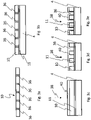
- Figure 3a shows a recording layer 10 or film according to the invention for generating stress in a solid.
- the film has at least one polymer material, in particular PDMS, with the polymer material having a lower glass transition at a temperature than 0°C, especially at a temperature below -50°C.
- the foil has a plurality of holes 36 for directing a liquid through the foil, the holes 36 each having a diameter of less than 0.1 mm.
- Figure 3b shows a solid 2 and a solid layer 4 separated from it.
- a receiving layer 10 or a film 10 is also arranged on the solid layer 4, by means of which the stresses required to produce a crack for separating the solid layer 4 from the solid 2 were generated.
- the absorption layer 10 has a multiplicity of holes for guiding a liquid, the absorption layer 10 being fixed to the solid layer 4 by means of a bonding layer 11 .
- 3c 1 shows, as an example for illustration, a receiving layer 10 or foil, which can be arranged or is arranged on the solid body 4, preferably likewise by means of a connecting layer 11.
- the receiving layer 10 preferably has a first material portion 39, in particular a polymer portion, and a second material portion 40, in particular a metal portion.
- the second material portion 40 preferably represents a coating of the first material portion 39 and is particularly preferably used for accelerated cooling of the first material portion 39.
- the recording layer 10 is preferably exposed to cold, in particular liquid nitrogen, from direction 38, whereby the second material portion 40 quickly cools down and, in particular, due to the direct contact with the first material portion 39, it is also cooled very quickly.
- 3d 1 shows, as a further illustrative example, an absorption layer 10 or film, which in turn is formed by the first material portion 39 and the second material portion 40.
- the first portion of material 39 has holes 36 which are filled by the second portion of material 40 .
- the second material portion 40 preferably also coats the first material portion 39 on the top side, i.e. parallel to the connecting layer 11.
- Figure 3e shows a further variant of the receiving layer 10 or film according to the invention, which in turn is formed by the first material portion 39 and the second material portion 40 .
- the first portion of material 39 has holes 36 which are lined by the second portion of material 40, ie the wall delimiting the respective hole 36 is coated with the second portion of material.
- the second material portion 40 preferably also coats the first material portion 39 on the top side, i.e. parallel to the connecting layer 11.
- the method for producing of solid layers comprises: providing a solid 2 for separating at least one solid layer 4, arranging an acquisition layer 10 for holding the solid layer 4 on the solid 2, the acquisition layer consisting of at least one polymer and another material, the acquisition layer preferably being the majority in terms of volume and/or mass consists of the polymer, with the other material having a higher conductivity than the polymer, thermal loading of the receiving layer 10 to generate, in particular mechanical, stresses in the solid body 2, the stresses causing a crack in the solid body 2 along a detachment plane 8 spreads, the solid layer 4 being separated from the solid 2 by the crack.
- the film according to the invention for generating stress in a solid has at least one polymer material, in particular PDMS, and a further material, with the film largely consisting of the polymer material in terms of volume, with the further material having a greater thermal conductivity than the polymer material, with the polymer material having a glass transition at a temperature of less than 0°C, in particular at a temperature of less than -50°C, the film having a large number of holes for conducting a liquid through the film, the holes each having a diameter of less than 0, have 1 mm.
Description
Die vorliegende Erfindung bezieht sich auf ein Verfahren zum Herstellen von Festkörperschichten.The present invention relates to a method for producing solid layers.
In vielen technischen Bereichen (z.B. Mikroelektronik- oder Photovoltaiktechnologie) werden Materialien, wie z.B. Silizium, Germanium oder Saphir, häufig in der Form dünner Scheiben und Platten (so genannte Wafer) gebraucht.In many technical areas (e.g. microelectronics or photovoltaic technology), materials such as silicon, germanium or sapphire are often used in the form of thin discs and plates (so-called wafers).
Die Druckschrift
Standardmäßig werden solche Wafer derzeit durch Sägen aus einem Ingot hergestellt, wobei relativ große Materialverluste ("kerf-loss") entstehen. Da das verwendete Ausgangsmaterial oft sehr teuer ist, gibt es starke Bestrebungen, solche Wafer mit weniger Materialaufwand und damit effizienter und kostengünstiger herzustellen. Beispielsweise gehen mit den derzeit üblichen Verfahren allein bei der Herstellung von Siliziumwafern für Solarzellen fast 50% des eingesetzten Materials als "kerf-loss" verloren. Weltweit gesehen entspricht dies einem jährlichen Verlust von über 2 Milliarden Euro. Da die Kosten des Wafers den größten Anteil an den Kosten der fertigen Solarzelle ausmachen (über 40%), könnten durch entsprechende Verbesserungen der Waferherstellung die Kosten von Solarzellen signifikant reduziert werden.By default, such wafers are currently produced by sawing from an ingot, with relatively large material losses (“kerf loss”) occurring. Since the starting material used is often very expensive, there are strong efforts to produce such wafers using less material and thus more efficiently and cost-effectively. For example, almost 50% of the material used is lost as "kerf-loss" in the production of silicon wafers for solar cells alone with the currently customary processes. Seen worldwide, this corresponds to an annual loss of over 2 billion euros. Since the cost of the wafer makes up the largest proportion of the cost of the finished solar cell (over 40%), the costs of solar cells could be significantly reduced by appropriate improvements in wafer production.
Besonders attraktiv für eine solche Waferherstellung ohne kerf-loss ("kerf-free wafering") erscheinen Verfahren, die auf das herkömmliche Sägen verzichten und z.B. durch Einsatz von temperaturinduzierten Spannungen direkt dünne Wafer von einem dickeren Werkstück abspalten können. Dazu gehören insbesondere Verfahren, wie sie z.B. in
Die Druckschriften
Die Polymerschicht weist bei den erwähnten Verfahren einen im Vergleich zum Werkstück um ungefähr zwei Größenordnungen höheren thermischen Ausdehnungskoeffizienten auf. Außerdem kann durch Ausnutzen eines Glasübergangs ein relativ hoher Elastizitätsmodul in der Polymerschicht erreicht werden, so dass im Schichtsystem Polymerschicht-Werkstück durch Abkühlen genügend große Spannungen induziert werden können, um die Abspaltung von Wafer vom Werkstück zu ermöglichen.In the processes mentioned, the polymer layer has a thermal expansion coefficient which is approximately two orders of magnitude higher than that of the workpiece. In addition, by utilizing a glass transition, a relatively high modulus of elasticity can be achieved in the polymer layer, so that sufficiently large stresses can be induced in the polymer layer-workpiece layer system by cooling to enable the wafer to be separated from the workpiece.
Beim Abspalten eines Wafers vom Werkstück haftet bei den erwähnten Verfahren jeweils auf einer Seite des Wafers noch Polymer an. Der Wafer krümmt sich dabei sehr stark in Richtung dieser Polymerschicht, was ein kontrolliertes Abspalten erschwert, und z.B. zu Dickenschwankungen des abgespaltenen Wafers führen kann. Außerdem erschwert die starke Krümmung die weitere Verarbeitung und kann sogar zum Zerbrechen des Wafers führen.When separating a wafer from the workpiece, polymer still adheres to one side of the wafer in the methods mentioned. The wafer curves very strongly in the direction of this polymer layer, which makes controlled cleavage more difficult and can lead to fluctuations in the thickness of the cleaved wafer, for example. In addition, the severe curvature complicates further processing and can even lead to breakage of the wafer.
Bei Verwendung der Verfahren nach bisherigem Stand der Technik weisen die hergestellten Wafer üblicherweise jeweils größere Dickenschwankungen auf, wobei die räumliche Dickenverteilung häufig ein Muster mit vierzähliger Symmetrie zeigt. Die totale Dickenschwankung über den ganzen Wafer gesehen ("total thickness variation", TTV) beträgt bei Verwendung der bisherigen Verfahren häufig mehr als 100% der mittleren Waferdicke (ein Wafer von bspw. 100 Mikrometer mittlerer Dicke, der z.B. an seiner dünnsten Stelle 50 Mikrometer dick und an seiner dicksten Stelle 170 Mikrometer dick ist, hat ein TTV von 170-50=120 Mikrometer, was relativ zu seiner mittleren Dicke einer totalen Dickenschwankung von 120% entspricht). Wafer mit solch starken Dickenschwankungen sind für viele Anwendungen nicht geeignet. Außerdem liegen bei den am häufigsten auftretenden vierzähligen Dickenverteilungsmustern die Bereiche mit den größten Schwankungen unglücklicherweise in der Mitte des Wafers, wo sie am meisten stören.Using the methods of the prior art, the wafers produced usually each exhibit larger variations in thickness, with the spatial thickness distribution often showing a pattern with four-fold symmetry. The total thickness variation seen over the entire wafer ("total thickness variation", TTV) is often more than 100% of the average wafer thickness when using the previous methods (a wafer of e.g. 100 micrometers average thickness, which is e.g. 50 micrometers at its thinnest point thick and 170 microns thick at its thickest point, has a TTV of 170-50=120 microns, which is a total thickness variation of 120% relative to its mean thickness). Wafers with such large variations in thickness are unsuitable for many applications. Also, for the most common four-fold thickness distribution patterns, the areas of greatest variation are unfortunately in the center of the wafer, where they are most disruptive.
Außerdem entstehen beim Verfahren nach aktuellem Stand der Technik während der Bruchpropagation beim Abspalten selbst unerwünschte Oszillationen in den beteiligten Schichtsystemen, die den Verlauf der Bruchfront ungünstig beeinflussen und insbesondere zu signifikanten Dickenschwankungen des abgespaltenen Wafers führen können.In addition, with the method according to the current state of the art, undesired oscillations occur in the layer systems involved during fracture propagation during splitting, which have an unfavorable influence on the course of the fracture front and, in particular, can lead to significant fluctuations in the thickness of the split wafer.
Ferner dauert das Ablösen der Polymerschicht von dem abgespalteten Wafer sehr lange, da beim Ablösen eine Flüssigkeit in den Zwischenraum von Folien und Wafer gelangen muss, wodurch die Polymerschicht sehr lange nicht zum Abtrennen eines weiteren Wafers verwendet werden kann.Furthermore, the detachment of the polymer layer from the cleaved wafer takes a very long time, since a liquid has to get into the space between the films and the wafer during detachment, as a result of which the polymer layer cannot be used for separating another wafer for a very long time.
Es ist somit die Aufgabe der vorliegenden Erfindung ein Verfahren zur Herstellung von Festkörperschichten bereitzustellen, das die kostengünstige und schnelle Herstellung von Festkörperplatten bzw. Wafern mit einer gleichmäßigen Dicke ermöglicht, insbesondere mit einem TTV von weniger als 120 Mikrometer.It is therefore the object of the present invention to provide a method for the production of solid layers, the cost-effective and quick production of Solid state wafers with a uniform thickness, particularly with a TTV of less than 120 microns.
Die zuvor genannte Aufgabe wird durch den Gegenstand der unabhängigen Ansprüche gelöst, die die vorliegende Erfindung definieren. Ausführungsformen, die nicht unter den Gegenstand der Ansprüche fallen, sind nicht Teil der vorliegenden Erfindung.The above object is solved by the subject matter of the independent claims defining the present invention. Embodiments that do not fall under the subject matter of the claims are not part of the present invention.
Ein Verfahren umfasst dabei mindestens die Schritte, Bereitstellen eines Festkörpers zum Abtrennen mindestens einer Festkörperschicht, Fixieren einer Aufnahmeschicht zum Halten der Festkörperschicht an dem Festkörper, wobei die Aufnahmeschicht eine Vielzahl an Löcher zum Leiten einer Flüssigkeit aufweist, wobei die Aufnahmeschicht mittels einer Verbindungsschicht an dem Festkörper fixiert wird und thermisches Beaufschlagen der Aufnahmeschicht zum, insbesondere mechanischen, Erzeugen von Spannungen in dem Festkörper, wobei sich durch die Spannungen ein Riss in dem Festkörper entlang einer Ablöseebene ausbreitet, wobei durch den Riss die Festkörperschicht von dem Festkörper abgetrennt wird.A method comprises at least the steps of providing a solid for separating at least one solid layer, fixing an acquisition layer to hold the solid layer on the solid, the acquisition layer having a large number of holes for conducting a liquid, the acquisition layer being attached to the solid by means of a connecting layer is fixed and thermal loading of the receiving layer for, in particular mechanical, generation of stresses in the solid body, the stresses causing a crack to propagate in the solid body along a detachment plane, the solid body layer being separated from the solid body by the crack.
Diese Lösung ist vorteilhaft, da durch die Löcher in der Aufnahmeschicht das Fluid zum Schwächen oder Zersetzen oder Auflösen der Verbindungsschicht sehr viel einfacher bzw. schneller bzw. in größeren Mengen an die Verbindungschicht heranführbar ist. In anderen Worten ist somit gemäß einer weiteren bevorzugten Ausführungsform der vorliegenden Erfindung zum Ablösen der Aufnahmeschicht von dem Festkörper ein Fluid, insbesondere eine Flüssigkeit, durch die Löcher der Verbindungsschicht zuführbar, wobei das Fluid bewirkt, dass die Fixierung der Aufnahmeschicht an dem Festkörper geschwächt oder aufgehoben wird.This solution is advantageous because the fluid for weakening or decomposing or dissolving the connecting layer can be fed to the connecting layer much more easily or faster or in larger quantities through the holes in the receiving layer. In other words, according to a further preferred embodiment of the present invention, a fluid, in particular a liquid, can be supplied through the holes in the connecting layer to detach the receiving layer from the solid, the fluid causing the fastening of the receiving layer to the solid to be weakened or eliminated will.
Die Löcher weisen gemäß der vorliegenden Erfindung einen Durchmesser von weniger als 0,1mm auf. Diese Ausführungsform ist vorteilhaft, da je kleiner die Löcher in der Aufnahmeschicht bzw. in der Folie sind, desto homogener bzw. ebener erfolgt eine Rissführung im Inneren des Festkörpers.According to the present invention, the holes have a diameter of less than 0.1 mm. This embodiment is advantageous because the smaller the holes in the receiving layer or in the film, the more homogeneous or level the cracks are in the interior of the solid body.
Die Aufnahmeschicht weist gemäß einer weiteren bevorzugten Ausführungsform der vorliegenden Erfindung mehr als 10 Löcher, bevorzugt mehr als 100 Löcher und besonders bevorzugt mehr als 1000 Löcher auf. Diese Ausführungsform ist vorteilhaft, da die Aufnahmeschicht bzw. Folie z.B. in bestimmten Regionen eine größere Löcheranzahl als in anderen Regionen aufweisen kann, wodurch in der Region mit der größeren Löcheranzahl bevorzugt mehr Flüssigkeit in der gleichen Zeit durch die Aufnahmeschicht hindurchleitbar ist. Bevorzugt weist die Aufnahmeschicht Flächenanteile auf, die je cm2 mehr als 1, 2, 3, 4, oder 5 Löcher, insbesondere mehr als 10 Löcher, insbesondere mehr als 50 Löcher, insbesondere mehre als 100 Löcher aufweist. Ferner ist denkbar, dass die Löcher in bestimmten Abschnitten der Aufnahmeschicht oder über die gesamte Aufnahmeschicht homogen verteilt sind.According to a further preferred embodiment of the present invention, the receiving layer has more than 10 holes, preferably more than 100 holes and particularly preferably more than 1000 holes. This embodiment is advantageous because the absorption layer or film can have a larger number of holes in certain regions than in other regions, whereby preferably more liquid can be conducted through the absorption layer at the same time in the region with the larger number of holes. The receiving layer preferably has surface areas which per cm 2 are more than 1, 2, 3, 4, or 5 holes, in particular more than 10 holes, in particular more than 50 holes, in particular more than 100 holes. It is also conceivable that the holes are distributed homogeneously in specific sections of the receiving layer or over the entire receiving layer.
In einem Radius von weniger als 50mm, bevorzugt weniger als 25mm und besonders bevorzugt weniger als 5mm, 4mm, 3mm, 2mm, 1mm oder 0,5mm, um das Zentrum eines jeden Loches herum ist gemäß einer weiteren bevorzugten Ausführungsform der vorliegenden Erfindung mindestens ein weiteres Loch ausgebildet. Diese Ausführungsform ist vorteilhaft, da durch diese Anordnung eine äußerst definierte und schnelle Fluidleitung durch die Aufnahmeschicht hindurch möglich ist.In a radius of less than 50mm, preferably less than 25mm and particularly preferably less than 5mm, 4mm, 3mm, 2mm, 1mm or 0.5mm, around the center of each hole is according to a further preferred embodiment of the present invention at least one more hole formed. This embodiment is advantageous because this arrangement enables extremely defined and rapid fluid conduction through the receiving layer.
Mittels mindestens einem Femtosekunden-Laser (fs-Laser), werden vor oder nach der Anbringung der Aufnahmeschicht an dem Festkörper Defekte in der inneren Struktur des Festkörpers zum Vorgeben der Ablöseebene erzeugt.By means of at least one femtosecond laser (fs-laser), defects are produced in the internal structure of the solid before or after the attachment of the recording layer to the solid in order to specify the detachment plane.
Diese Lösung ist vorteilhaft, da aufgrund der Strahlungsquelle die Ablöseschicht bzw. Defektschicht in dem Festkörper erzeugbar ist, durch die der Riss bei der Rissausbreitung geleitet bzw. geführt wird, was die Realisierung sehr kleiner TTVs, insbesondere kleiner als 200 Mikrometer oder 100 Mikrometer oder kleiner als 80 Mikrometer oder kleiner als 60 Mikrometer oder kleiner als 40 Mikrometer oder kleiner als 20 Mikrometer oder kleiner als 10 Mikrometer oder kleiner als 5 Mikrometer, insbesondere 4, 3, 2 oder 1 Mikrometer, ermöglicht. Die Strahlenbeaufschlagung des Wafers schafft somit in einem ersten Schritt eine Art Perforation im Inneren des Festkörpers, entlang der in einem zweiten Schritt die Rissausbreitung erfolgt bzw. entlang der die Festkörperschicht von dem Festkörper abgetrennt wird.This solution is advantageous because due to the radiation source, the detachment layer or defect layer can be generated in the solid body, through which the crack is guided or guided during crack propagation, which allows the realization of very small TTVs, in particular smaller than 200 micrometers or 100 micrometers or smaller than 80 micrometers or smaller than 60 micrometers or smaller than 40 micrometers or smaller than 20 micrometers or smaller than 10 micrometers or smaller than 5 micrometers, in particular 4, 3, 2 or 1 micrometer. The exposure of the wafer to radiation thus creates in a first step a kind of perforation in the interior of the solid body, along which the crack propagation takes place in a second step or along which the layer of solid body is separated from the solid body.
Durch die defektbedingte Rissführung wird verhindert, dass die Löcher in der Aufnahmeschicht einen Einfluss auf die Topografie der durch den Riss entstehenden Oberflächenstruktur haben bzw. der Einfluss der Löcher auf die Topografie sehr stark reduziert wird. Durch die Defekte bzw. Laservorschädigung wird nämlich erreicht, dass der Riss ausreichend stabil in der durch die Defekte definierten Rissebene bzw. Risskontur verläuft.The guidance of the cracks caused by the defect prevents the holes in the recording layer from having an influence on the topography of the surface structure created by the crack, or the influence of the holes on the topography is greatly reduced. The defects or laser pre-damage ensure that the crack runs sufficiently stably in the crack plane or crack contour defined by the defects.
Gemäß einer bevorzugten Ausführungsform der vorliegenden Erfindung hat der Laser eine Pulsdauer unter 500fs.According to a preferred embodiment of the present invention, the laser has a pulse duration of less than 500 fs.
Die Spannungen zum Ablösen der Festkörperschicht von dem Festkörper werden durch die thermische Beaufschlagung der Aufnahmeschicht erzeugt, wobei die Aufnahmeschicht zumindest einen Polymerwerkstoff aufweist, wobei der Polymerwerkstoff einen Glasübergang bei einer Temperatur kleiner 0°C erfährt. Die thermische Beaufschlagung stellt ein Abkühlen der Aufnahmeschicht bzw Polymerschicht unter 0°C und bevorzugt unter -10°C dar. Die Abkühlung der Polymerschicht erfolgt derart, dass zumindest ein Teil der Polymerschicht, die bevorzugt aus PDMS besteht, einen Glasübergang vollzieht. Die Abkühlung kann hierbei eine Abkühlung auf unter -100°C sein, die z.B. mittels flüssigen Stickstoffs bewirkbar ist. Diese Ausführungsform ist vorteilhaft, da sich die Polymerschicht in Abhängigkeit von der Temperaturveränderung zusammenzieht und/oder einen Glasübergang erfährt und die dabei entstehenden Kräfte auf den Festkörper überträgt, wodurch mechanische Spannungen in dem Festkörper erzeugbar sind, die zum Auslösen eines Risses und/oder zur Rissausbreitung führen, wobei sich der Riss zunächst entlang der ersten Ablöseebene zum Abspalten der Festkörperschicht ausbreitet.The stresses for detaching the solid layer from the solid are generated by the thermal loading of the receiving layer, the receiving layer having at least one polymer material, the polymer material experiencing a glass transition at a temperature below 0°C. the thermal exposure represents cooling of the receiving layer or polymer layer below 0° C. and preferably below -10° C. The polymer layer is cooled in such a way that at least part of the polymer layer, which preferably consists of PDMS, undergoes a glass transition. In this case, the cooling can be a cooling to below -100° C., which can be effected, for example, by means of liquid nitrogen. This embodiment is advantageous because the polymer layer contracts as a function of the temperature change and/or undergoes a glass transition and the resulting forces are transferred to the solid body, as a result of which mechanical stresses can be generated in the solid body, which trigger a crack and/or crack propagation lead, the crack initially propagating along the first detachment plane to split off the solid layer.
Gemäß einer bevorzugten Ausführungsform der vorliegenden Erfindung wird der Festkörper an einer Halteschicht zum Halten des Festkörpers angeordnet, wobei die Halteschicht an einem ersten ebenen Flächenanteil des Festkörpers angeordnet wird, wobei der erste ebene Flächenanteil des Festkörpers von einem zweiten ebenen Flächenanteil des Festkörpers beabstandet ist, wobei am zweiten ebenen Flächenanteil die Polymerschicht angeordnet ist und wobei die Ablöseebene gegenüber dem ersten ebenen Flächenanteil und/oder dem zweiten ebenen Flächenanteil parallel ausgerichtet wird bzw. parallel erzeugt wird.According to a preferred embodiment of the present invention, the solid is arranged on a holding layer for holding the solid, the holding layer being arranged on a first planar surface portion of the solid, the first planar surface portion of the solid being spaced from a second planar surface portion of the solid, wherein the polymer layer is arranged on the second flat surface portion and the detachment plane is aligned parallel to the first flat surface portion and/or the second flat surface portion or is produced parallel.
Diese Ausführungsform ist vorteilhaft, da der Festkörper zumindest abschnittweise und bevorzugt vollständig zwischen der Halteschicht und der Polymerschicht angeordnet ist, wodurch mittels einer dieser Schichten oder mittels beider Schichten die Spannungen zur Risserzeugung bzw. Rissausbreitung in den Festkörper einleitbar sind.This embodiment is advantageous because the solid is arranged at least in sections and preferably completely between the retaining layer and the polymer layer, whereby the stresses for crack generation or crack propagation can be introduced into the solid by means of one of these layers or by means of both layers.
Mindestens oder genau eine Strahlungsquelle ist gemäß der vorliegenden Erfindung zum Bereitstellen der in den Festkörper einzubringenden Strahlung derart konfiguriert, dass die von ihr ausgestrahlten Strahlen die Defekte an vorbestimmten Orten innerhalb des Festkörpers erzeugen. Diese Ausführungsform ist vorteilhaft, da mittels einer Strahlungsquelle, insbesondere mittels eines Lasers, äußerst genau Defekte in dem Festkörper erzeugbar sind.According to the present invention, at least or precisely one radiation source is configured for providing the radiation to be introduced into the solid in such a way that the rays emitted by it produce the defects at predetermined locations within the solid. This embodiment is advantageous since defects can be produced in the solid body extremely precisely by means of a radiation source, in particular by means of a laser.
Für das Verfahren ergeben sich insbesondere zwei Anwendungsfälle, im Folgenden "Wafering" und "thinning" genannt. Beim "Wafering" wird das Verfahren üblicherweise dafür genutzt eine dicke Schicht von einem noch dickeren Halbleiterblock abzulösen, typischerweise einen Wafer (mit den industriespezifischen Dicken) von einem Ingot. Beim "Thinning" wird das Verfahren dafür eingesetzt, von einem Wafer eine sehr dünne Schicht abzuspalten, was dem heutigen Prozess des grindings entspricht, allerdings mit dem Vorteil, dass das nicht benötigte Material unversehrt bleibt und wiederverwendet werden kann. Eine klare Trennung von "thinning" und "Wafering" ist kompliziert, weil z.B. das "thinning" auch durch Beaufschlagung von der Rückseite eines Wafers geschehen kann, so dass zwar eine dünne Schicht entsteht, der Laser aber tief in das Material eindringt.There are in particular two applications for the method, referred to below as “wafering” and “thinning”. In "wafering," the process is commonly used to strip a thick layer from an even thicker semiconductor ingot, typically a wafer (of industry-specific thicknesses) from an ingot. With "thinning", the process is used to split off a very thin layer from a wafer, which corresponds to today's grinding process, but with the advantage that material that is not required remains intact and can be reused. A clear separation of "thinning" and "wafering" is complicated because, for example, "thinning" is too by hitting it from the back of a wafer, so that although a thin layer is formed, the laser penetrates deep into the material.
Für den "thinning" Fall :
Die Strahlungsquelle wird gemäß einer weiteren bevorzugten Ausführungsform der vorliegenden Erfindung derart eingestellt, dass die von ihr ausgestrahlten Strahlen zum Erzeugen der Ablöseebene auf eine definierte Tiefe, insbesondere <100µm, in den Festkörper eindringen. Bevorzugt wird die Ablöseebene parallel beabstandet zu einer äußeren und bevorzugt ebenen Oberfläche des Festkörpers ausgebildet. Bevorzugt ist die Ablöseebene weniger als 100 Mikrometer und bevorzugt weniger als 50 Mikrometer und besonders bevorzugt weniger als oder gleich 20, 10, 5 oder 2 Mikrometer von der ebenen Oberfläche des Festkörpers beabstandet innerhalb des Festkörpers ausgebildet. Somit wird die Ablöseebene bevorzugt in Form einer aus Defekten erzeugten Ebene ausgebildet, wobei die Defekte weniger als 100 Mikrometer und bevorzugt weniger als 50 Mikrometer und besonders bevorzugt weniger als 20, 10 oder 2 Mikrometer von der ebenen Oberfläche des Festkörpers beabstandet innerhalb des Festkörpers ausgebildet werden.For the "thinning" case:
According to a further preferred embodiment of the present invention, the radiation source is set in such a way that the rays emitted by it penetrate the solid body to a defined depth, in particular <100 μm, to produce the detachment plane. The detachment plane is preferably formed at a parallel distance from an outer and preferably planar surface of the solid body. Preferably, the detachment plane is formed within the solid at a distance of less than 100 microns, and preferably less than 50 microns, and more preferably less than or equal to 20, 10, 5, or 2 microns from the planar surface of the solid. Thus, the detachment plane is preferably formed in the form of a plane created from defects, the defects being formed within the solid at less than 100 microns and preferably less than 50 microns and more preferably less than 20, 10 or 2 microns from the planar surface of the solid .
Für den "wafering" Fall :
Die Strahlungsquelle wird gemäß einer weiteren bevorzugten Ausführungsform der vorliegenden Erfindung derart eingestellt, dass die von ihr ausgestrahlten Strahlen zum Erzeugen der Ablöseebene auf eine definierte Tiefe, insbesondere >100µm, in den Festkörper eindringen. Bevorzugt wird die Ablöseebene parallel beabstandet zu einer äußeren und bevorzugt ebenen Oberfläche des Festkörpers ausgebildet. Bevorzugt ist die Ablöseebene mehr als 100 Mikrometer und bevorzugt mehr als 200 Mikrometer und besonders bevorzugt mehr als 400 oder 700 Mikrometer von der ebenen Oberfläche des Festkörpers beabstandet innerhalb des Festkörpers ausgebildet. Somit wird die Ablöseebene bevorzugt in Form einer aus Defekten erzeugten Ebene ausgebildet, wobei die Defekte mehr als 100 Mikrometer und bevorzugt mehr als 200 Mikrometer und besonders bevorzugt mehr als 400 oder 700 Mikrometer von der ebenen Oberfläche des Festkörpers beabstandet innerhalb des Festkörpers ausgebildet werden.For the "wafering" case:
According to a further preferred embodiment of the present invention, the radiation source is adjusted in such a way that the rays emitted by it penetrate the solid body to a defined depth, in particular >100 μm, to produce the detachment plane. The detachment plane is preferably formed at a parallel distance from an outer and preferably planar surface of the solid body. Preferably, the detachment plane is formed within the solid at a distance of more than 100 microns and preferably more than 200 microns and more preferably more than 400 or 700 microns from the planar surface of the solid. Thus, the detachment plane is preferably formed in the form of a plane created from defects, the defects being formed within the solid at a distance greater than 100 microns and preferably greater than 200 microns and more preferably greater than 400 or 700 microns from the planar surface of the solid.
Der Festkörper wird gemäß einer weiteren bevorzugten Ausführungsform der vorliegenden Erfindung mit einer vorgegebenen Wellenlänge und/oder Leistung beaufschlagt, wobei die vorgegebene Wellenlänge bevorzugtan das jeweilige Material bzw. Substrat angepasst ist. Diese Ausführungsform ist vorteilhaft, da die Defektgröße durch die Wellenlänge und/oder die Leistung beeinflussbar ist.According to a further preferred embodiment of the present invention, the solid body is subjected to a predetermined wavelength and/or power, the predetermined wavelength preferably being adapted to the respective material or substrate. This embodiment is advantageous since the defect size can be influenced by the wavelength and/or the power.
Der Festkörper weist gemäß einer weiteren bevorzugten Ausführungsform der vorliegenden Erfindung Silizium und/oder Gallium oder Perowskit auf und die Polymerschicht und/oder die Halteschicht bestehen zumindest teilweise und bevorzugt vollständig oder zu mehr als 75% aus Polydimethylsiloxane (PDMS), wobei die Halteschicht an einer zumindest abschnittsweise ebenen Fläche einer Stabilisierungseinrichtung angeordnet ist, die zumindest teilweise aus mindestens einem Metall besteht. Die Stabilisierungseinrichtung ist bevorzugt eine Platte, insbesondere eine Platte die Aluminium aufweist oder daraus besteht. Diese Ausführungsform ist vorteilhaft, da durch die Stabilisierungseinrichtung und die Halteschicht der Festkörper definiert bzw. fest gehalten wird, wodurch die Spannungen sehr genau in dem Festkörper erzeugt werden können.According to a further preferred embodiment of the present invention, the solid body has silicon and/or gallium or perovskite and the polymer layer and/or the retaining layer consist at least partially and preferably completely or to more than 75% of polydimethylsiloxane (PDMS), the retaining layer being attached to a at least partially flat surface of a stabilization device is arranged, which consists at least partially of at least one metal. The stabilization device is preferably a plate, in particular a plate that has aluminum or consists of it. This embodiment is advantageous because the solid body is defined or held firmly by the stabilization device and the holding layer, as a result of which the stresses can be generated very precisely in the solid body.
Gemäß einer weiteren bevorzugten Ausführungsform der vorliegenden Erfindung sind die Spannungen in dem Festkörper derart einstellbar bzw. erzeugbar, dass die Rissauslösung und/oder die Rissausbreitung zum Erzeugen einer Topografie der sich in der Rissebene ergebenden Oberfläche steuerbar ist. Die Spannungen sind somit bevorzugt in unterschiedlichen Bereichen des Festkörpers bevorzugt zumindest zeitweise unterschiedlich stark erzeugbar. Diese Ausführungsform ist vorteilhaft, da durch Steuerung der Rissauslösung und/oder des Rissverlaufs die Topographie der erzeugten bzw. abgetrennten Festkörperschicht vorteilhaft beeinflussbar ist.According to a further preferred embodiment of the present invention, the stresses in the solid body can be set or generated in such a way that crack initiation and/or crack propagation can be controlled to generate a topography of the surface resulting in the plane of the crack. The stresses can thus preferably be generated to different degrees in different regions of the solid body, preferably at least at times. This embodiment is advantageous because the topography of the produced or separated solid layer can be advantageously influenced by controlling the initiation of the crack and/or the course of the crack.
Gemäß einer weiteren bevorzugten Ausführungsform der vorliegenden Erfindung geben die Defekte mindestens eine Rissführungsschicht vor, wobei die mindestens eine Rissführungsschicht eine von einer ebenen Gestalt abweichende Gestalt aufweist. Diese Lösung ist vorteilhaft, da die erzeugten Festkörperschichten oder die erzeugten Festkörper eine von einer ebenen Schicht abweichende Gestalt aufweisen können. Es können somit nicht mehr nur ebene Schichten, sondern ebenfalls dreidimensionale Körper aus einem Werkstück mittels einer Rissausbreitung herausgebildet bzw. erzeugt werden. Derart hergestellte Festkörper weisen aufgrund des Herstellungsverfahrens eine sehr vorteilhafte und nur wenig bis nicht nachzubearbeitende Oberfläche auf. So sind z.B. optische Elemente, wie z.B. ein Spat oder eine Linse in einem einstufigen oder mehrstufigen, insbesondere zwei oder dreistufigen, Splitprozess herstellbar.According to a further preferred embodiment of the present invention, the defects define at least one crack guiding layer, wherein the at least one crack guiding layer has a shape that deviates from a planar shape. This solution is advantageous since the solid layers produced or the solid bodies produced can have a shape that deviates from a planar layer. It is therefore no longer only possible to form or produce flat layers, but also three-dimensional bodies from a workpiece by means of crack propagation. Due to the manufacturing process, solid bodies produced in this way have a very advantageous surface that requires little or no post-processing. For example, optical elements such as a spar or a lens can be produced in a single-stage or multi-stage, in particular two or three-stage, splitting process.
Die Gestalt der Rissführungsschicht weist somit gemäß einer bevorzugten Ausführungsform der vorliegenden Erfindung zumindest abschnittsweise die Kontur eines dreidimensionalen Objektes, insbesondere einer Linse oder eines Spaten, auf.According to a preferred embodiment of the present invention, the shape of the crack-guiding layer thus has, at least in sections, the contour of a three-dimensional object, in particular a lens or a spade.
Gemäß einer bevorzugten Ausführungsform der vorliegenden Erfindung werden die Defekte mittels einer Defekterzeugungsvorrichtung bzw. der Strahlungsquelle erzeugt, wobei die Defekterzeugungsvorrichtung derart konfiguriert ist, dass die Defekte mit einem konstanten Abstand zur Defekterzeugungsvorrichtung in dem Werkstück erzeugt werden, wobei das Werkstück und die Defekterzeugungsvorrichtung derart relativ zueinander geneigt werden, dass die von der Defekterzeugungsvorrichtung erzeugten Defekte in der Rissführungsschicht erzeugt werden, wobei die Defekterzeugungsvorrichtung und das Werkstück während der Defekterzeugung lediglich zweidimensional zueinander umpositioniert werden. Die Defekterzeugungsvorrichtung wird somit bevorzugt gegenüber dem Werkstück umpositioniert oder das Werkstück wird gegenüber der Defekterzeugungsvorrichtung umpositioniert oder die Defekterzeugungsvorrichtung und das Werkstück werden beide zueinander umpositioniert.According to a preferred embodiment of the present invention, the defects are generated by means of a defect generation device or the radiation source, the defect generation device being configured in such a way that the defects have a constant distance to the defect generation device in the workpiece, the workpiece and the defect generation device being inclined relative to one another in such a way that the defects generated by the defect generation device are generated in the crack guiding layer, the defect generation device and the workpiece being repositioned only two-dimensionally relative to one another during the defect generation. The defect generating device is thus preferably repositioned relative to the workpiece, or the workpiece is repositioned relative to the defect generating device, or the defect generating device and the workpiece are both repositioned relative to one another.
Diese Ausführungsform ist vorteilhaft, da die Strahlungsquelle bzw. die Defekterzeugungseinrichtung zur Defekterzeugung lediglich umpositioniert werden muss und keine Modifikation der Defekterzeugungsvorrichtung bewirkt werden muss, insbesondere keine veränderte Defekteinbringtiefe bestimmt und eingestellt werden muss.This embodiment is advantageous because the radiation source or the defect generation device only has to be repositioned for defect generation and no modification of the defect generation device has to be effected, in particular no changed defect insertion depth has to be determined and set.
Die Defekte werden gemäß einer weiteren bevorzugten Ausführungsform mittels einer Defekterzeugungsvorrichtung bzw. der Strahlungsquelle erzeugt, wobei die Defekterzeugungsvorrichtung derart konfiguriert ist, dass die Defekte mit einem sich zeitweise veränderndem Abstand zur Defekterzeugungsvorrichtung in dem Werkstück erzeugt werden, wobei in Abhängigkeit von dem Abstand der Defekterzeugungsvorrichtung zu dem zu erzeugenden Defekts zumindest zeitweise eine Modifikation der Defekterzeugungsvorrichtung bewirkt wird, insbesondere eine veränderte Defekteinbringtiefe bestimmt und eingestellt wird. Diese Ausführungsform ist vorteilhaft, da bevorzugt keine Neigungsvorrichtung zum Neigen des Werkstücks vorgesehen werden muss.According to a further preferred embodiment, the defects are generated by means of a defect generation device or the radiation source, the defect generation device being configured in such a way that the defects are generated in the workpiece at a temporarily changing distance from the defect generation device, depending on the distance of the defect generation device the defect to be generated, at least temporarily a modification of the defect generating device is effected, in particular a changed defect insertion depth is determined and set. This embodiment is advantageous because preferably no tilting device has to be provided for tilting the workpiece.
Der Festkörper weist bevorzugt ein Material oder eine Materialkombination aus einer der Hauptgruppen 3, 4 und 5 des Periodensystems der Elemente auf, wie z.B. Si, SiC, SiGe, Ge, GaAs, InP, GaN, Al2O3 (Saphir), AIN. Besonders bevorzugt weist der Festkörper eine Kombination aus in der dritten und fünften Gruppe des Periodensystems vorkommenden Elementen auf. Denkbare Materialien oder Materialkombinationen sind dabei z.B. Galliumarsenid, Silizium, Siliziumcarbid, etc. Weiterhin kann der Festkörper eine Keramik (z.B. Al2O3 - Alumiumoxid) aufweisen oder aus einer Keramik bestehen, bevorzugte Keramiken sind dabei z.B. Perovskitkeramiken (wie z.B. Pb-, O-, Ti/Zr-haltige Keramiken) im Allgemeinen und Blei-Magnesium-Niobate, Bariumtitanat, Lithiumtitanat, Yttrium-Aluminium-Granat, insbesondere Yttrium-Aluminium-Granat Kristalle für Festkörperlaseranwendungen, SAW-Keramiken (surface acoustic wave), wie z.B. Lithiumniobat, Galliumorthophosphat, Quartz, Calziumtitanat, etc. im Speziellen. Der Festkörper weist somit bevorzugt ein Halbleitermaterial oder ein Keramikmaterial auf bzw. besonders bevorzugt besteht der Festkörper aus mindestens einem Halbleitermaterial oder einem Keramikmaterial. Es ist weiterhin denkbar, dass der Festkörper ein transparentes Material aufweist oder teilweise aus einem transparenten Material, wie z.B. Saphir, besteht bzw. gefertigt ist. Weitere Materialien, die hierbei als Festkörpermaterial alleine oder in Kombination mit einem anderen Material in Frage kommen, sind z.B. "wide band gap"-Materialien, InAISb, Hochtemperatursupraleiter, insbesondere seltene Erden Cuprate (z.B. YBa2Cu3O7).The solid preferably has a material or a material combination from one of the
Gemäß der vorliegenden Erfindung ist die Strahlungsquelle oder ein Teil der Strahlungsquelle als Femtosekundenlaser (fs-Laser) ausgebildet. Diese Lösung ist vorteilhaft, da durch die Verwendung eines fs-Laser, die vertikale Ausbreitung des gestörten Materials minimiert wird. Es ist durch die Verwendung eines fs-Lasers möglich Defekte in dem Werkstück sehr genau einzubringen bzw. darin zu erzeugen. Die Wellenlänge und/oder die Energie des fs-Laser sind bevorzugt materialabhängig zu wählen.According to the present invention, the radiation source or part of the radiation source is designed as a femtosecond laser (fs laser). This solution is advantageous because the use of an fs laser minimizes the vertical propagation of the disturbed material. By using an fs-laser it is possible to introduce defects in the workpiece very precisely or to create them therein. The wavelength and/or the energy of the fs laser should preferably be chosen depending on the material.
Gemäß einer weiteren bevorzugten Ausführungsform der vorliegenden Erfindung wird die Energie des fs-Lasers, derart gewählt, dass die Schädigungsausbreitung im Festkörper bzw. im Kristall kleiner als dreimal die Reyleighlänge, bevorzugt kleiner als die Reyleighlänge und besonders bevorzugt kleiner als ein Drittel der Reyleighlänge ist.According to a further preferred embodiment of the present invention, the energy of the fs laser is selected such that the damage propagation in the solid or in the crystal is less than three times the Reyleigh length, preferably less than the Reyleigh length and particularly preferably less than one third of the Reyleigh length.
Die Wellenlänge des Laserstrahls des fs-Lasers wird gemäß einer weiteren bevorzugten Ausführungsform der vorliegenden Erfindung derart gewählt, dass die Absorption des Festkörpers bzw. des Materials kleiner als 10cm-1 und bevorzugt kleiner als 1cm-1 und besonders bevorzugt kleiner als 0,1cm-1 ist.According to a further preferred embodiment of the present invention, the wavelength of the laser beam of the fs laser is selected in such a way that the absorption of the solid body or the material is less than 10 cm -1 and preferably less than 1 cm -1 and particularly preferably less than 0.1 cm - 1 is
Die einzelnen Defekte resultieren gemäß einer weiteren bevorzugten Ausführungsform der vorliegenden Erfindung jeweils aus einer von dem fs-Laser bewirkten multi-photonen Anregung.According to a further preferred embodiment of the present invention, the individual defects each result from multi-photon excitation brought about by the fs laser.
Weiterhin ist gemäß einer weiteren bevorzugten Ausführungsform der vorliegenden Erfindung denkbar, dass die Aufnahmeschicht einen weiteren Werkstoff aufweist, der bevorzugt als Beschichtung auf das Polymer aufgebracht ist. Alternativ ist jedoch ebenfalls denkbar, dass das Polymer als Beschichtung auf den weiteren Werkstoff aufgebracht ist.Furthermore, according to a further preferred embodiment of the present invention, it is conceivable that the receiving layer has a further material which is preferably applied to the polymer as a coating. Alternatively, however, it is also conceivable that the polymer is applied to the additional material as a coating.
Gemäß einer weiteren bevorzugten Ausführungsform der vorliegenden Erfindung weist die Beschichtung lokale Schwächungen auf, insbesondere ist die Beschichtung gebrochen, insbesondere um einer durch das Polymer bei der Spannungserzeugung bewirkten Verformung zu folgen.According to a further preferred embodiment of the present invention, the coating has local weaknesses, in particular the coating is broken, in particular in order to follow a deformation caused by the polymer when stress is generated.
Die Wärmeleitfähigkeit (W/(m*K)) des weiteren Werkstoffs ist gemäß einer weiteren bevorzugten Ausführungsform der vorliegenden Erfindung mehr als 5 mal größer, bevorzugt mehr als 10 mal größer und besonders bevorzugt mehr als 30, mehr als 100, mehr als 200 oder mehr als 300 mal größer als die des Polymers, wobei der weitere Werkstoff bevorzugt ein Metall oder eine Legierung ist.According to a further preferred embodiment of the present invention, the thermal conductivity (W/(m*K)) of the further material is more than 5 times greater, preferably more than 10 times greater and particularly preferably more than 30, more than 100, more than 200 or more than 300 times greater than that of the polymer, the further material preferably being a metal or an alloy.
Der weitere Werkstoff ist gemäß einer weiteren bevorzugten Ausführungsform der vorliegenden Erfindung in Form von länglichen Elementen, insbesondere Spänen, innerhalb einer von dem Polymer vorgegebenen Schichtstruktur vorgesehen, wobei die Späne bevorzugt derart ausgerichtet sind, dass sich ihrer Längsachsen (bevorzugt zumindest mehrheitlich) geneigt, insbesondere orthogonal, zur Schichterstreckungsrichtung erstreckt. Bevorzugt werden dazu die Späne beim Erzeugen der Aufnahmeschicht in das flüssige Polymer eingebracht und z.B. über eine Magnetbeaufschlagung ausgerichtet.According to a further preferred embodiment of the present invention, the further material is provided in the form of elongate elements, in particular chips, within a layer structure predetermined by the polymer, with the chips preferably being aligned in such a way that their longitudinal axes (preferably at least mostly) incline, in particular orthogonal to the layer extension direction. For this purpose, the chips are preferably introduced into the liquid polymer during the production of the receiving layer and aligned, for example, by applying a magnet.
Die vorliegende Erfindung bezieht sich ferner auf eine wiederverwendbare Folie zur Spannungserzeugung in einem Festkörper, wobei die Folie zumindest einen Polymerwerkstoff, insbesondere PDMS, aufweist, wobei der Polymerwerkstoff einen Glasübergang bei einer Temperatur kleiner als 0°C, insbesondere bei einer Temperatur kleiner -50°C, erfährt. Die Folie weist eine Vielzahl an Löchern zum Leiten einer Flüssigkeit auf, wobei die Löcher jeweils einen Durchmesser von weniger als 0,1mm aufweisen. Weiterhin werden die Gegenstände der Druckschriften
Weitere Vorteile, Ziele und Eigenschaften der vorliegenden Erfindung werden anhand nachfolgender Beschreibung anliegender Zeichnungen erläutert, in welchen beispielhaft die erfindungsgemäße Waferherstellung dargestellt ist. Bauteile oder Elemente der erfindungsgemäßen Waferherstellung, welche in den Figuren wenigstens im Wesentlichen hinsichtlich ihrer Funktion übereinstimmen, können hierbei mit gleichen Bezugszeichen gekennzeichnet sein, wobei diese Bauteile oder Elemente nicht in allen Figuren beziffert oder erläutert sein müssen.Further advantages, goals and properties of the present invention are explained with reference to the following description of the accompanying drawings, in which the wafer production according to the invention is shown by way of example. Components or elements of the wafer production according to the invention, which in the figures at least essentially match in terms of their function can be identified with the same reference numerals, these components or elements need not be numbered or explained in all figures.
Darin zeigt:
- Fig. 1a
- einen schematischen Aufbau zum Erzeugen von Lokal-Spannungen in einem Festkörper;
- Fig. 1b
- eine schematische Darstellung einer Schichtanordnung vor dem Abtrennen einer Festkörperschicht von einem Festkörper;
- Fig. 1c
- eine schematische Darstellung einer Schichtanordnung nach dem Abtrennen einer Festkörperschicht von einem Festkörper;
- Fig. 2a
- eine erste schematisch dargestellte Variante zur Erzeugung von Lokal-Spannungen mittels Strahlung, insbesondere Lichtwellen;
- Fig. 2b
- eine zweite schematisch dargestellte Variante zur Erzeugung von Lokal-Spannungen mittels Strahlung, insbesondere mittels Lichtwellen;
- Fig. 3a
- eine erfindungsgemäße Aufnahmeschicht;
- Fig. 3b
- eine erfindungsgemäße Aufnahmeschicht, die an einem Festkörper angeordnet ist;
- Fig. 3c
- eine weitere Aufnahmeschicht, die an einem Festkörper angeordnet ist; Dieses Beispiel stellt jedoch kein Ausführungsbeispiel der beanspruchten Erfindung dar.
- Fig. 3d
- eine weitere Aufnahmeschicht, die an einem Festkörper angeordnet ist; und
- Fig. 3e
- eine vierte erfindungsgemäße Aufnahmeschicht, die an einem Festkörper angeordnet ist.
- Fig. 1a
- a schematic structure for generating local stresses in a solid;
- Fig. 1b
- a schematic representation of a layer arrangement before the separation of a solid layer from a solid;
- 1c
- a schematic representation of a layer arrangement after the separation of a solid layer from a solid;
- Figure 2a
- a first schematically illustrated variant for generating local voltages by means of radiation, in particular light waves;
- Figure 2b
- a second schematically illustrated variant for generating local voltages by means of radiation, in particular by means of light waves;
- Figure 3a
- a recording layer according to the invention;
- Figure 3b
- a recording layer according to the invention, which is arranged on a solid;
- 3c
- another acquisition layer disposed on a solid; However, this example does not constitute an embodiment of the claimed invention.
- 3d
- another acquisition layer disposed on a solid; and
- Figure 3e
- a fourth acquisition layer according to the invention, which is arranged on a solid body.
In
In
In
In den
Die vorliegende Erfindung bezieht sich somit auf ein Verfahren zum Herstellen von Festkörperschichten, mindestens umfassend die Schritte nach Anspruch 1. Das erfindungsgemäße Verfahren kann dabei zusätzlich einen, mehrere oder alle der nachfolgend angeführten Schritte, insbesondere des Bereitstellens eines Werkstücks 2 zum Abtrennen mindestens einer Festkörperschicht 4, des Erzeugens von bevorzugt definierten Lokal-Spannungen bzw. von lokalen Spannungen mittels mindestens einer Strahlungsquelle, insbesondere einem fs-Laser, in der inneren Struktur des Festkörpers zum Vorgeben einer Rissführungsschicht, entlang der die Festkörperschicht vom Festkörper abgetrennt wird, und des thermischen Beaufschlagens einer an dem Werkstück 2 angeordneten Polymerschicht 10 zum, insbesondere mechanischen, Erzeugen von Ablöse-Spannungen in dem Werkstück 2, wobei sich durch die Ablöse-Spannungen ein Riss in dem Werkstück 2 entlang der Rissführungsschicht 8 ausbreitet, der die Festkörperschicht 4 von dem Werkstück 2 abtrennt, umfassen. Die Lokal-Spannungen bewirken hierbei bevorzugt, dass die Rissausbreitung in der gewünschten Rissführungsschicht 8 erfolgt.The present invention thus relates to a method for producing solid layers, at least comprising the steps according to claim 1. The method according to the invention can additionally include one, several or all of the steps listed below, in particular the provision of a
In
In
Die Folie weist eine Vielzahl an Löcher 36 zum Leiten einer Flüssigkeit durch die Folie hindurch auf, wobei die Löcher 36 jeweils einen Durchmesser von weniger als 0,1mm aufweisen.The foil has a plurality of
Ferner ist bevorzugt zusätzlich denkbar, dass das Verfahren zum Herstellen von Festkörperschichten, einen, mehrere oder alle der nachfolgend genannten Schritte umfasst: Bereitstellen eines Festkörpers 2 zum Abtrennen mindestens einer Festkörperschicht 4, Anordnen einer Aufnahmeschicht 10 zum Halten der Festkörperschicht 4 an dem Festkörper 2, wobei die Aufnahmeschicht zumindest aus einem Polymer und einem weiteren Werkstoff besteht, wobei die Aufnahmeschicht bevorzugt volumenmäßig und/oder massemäßig mehrheitlich aus dem Polymer besteht, wobei der weitere Werkstoff eine größere Leitfähigkeit als das Polymer aufweist, thermisches Beaufschlagen der Aufnahmeschicht 10 zum, insbesondere mechanischen, Erzeugen von Spannungen in dem Festkörper 2, wobei sich durch die Spannungen ein Riss in dem Festkörper 2 entlang einer Ablöseebene 8 ausbreitet, wobei durch den Riss die Festkörperschicht 4 von dem Festkörper 2 abgetrennt wird.Furthermore, it is preferably additionally conceivable that the method for producing of solid layers, one, several or all of the steps mentioned below comprises: providing a solid 2 for separating at least one
Weiterhin weist die erfindungsgemäße Folie zur Spannungserzeugung in einem Festkörper, zumindest einen Polymerwerkstoff, insbesondere PDMS, und einen weiteren Werkstoff auf, wobei die Folie volumenmäßig mehrheitlich aus dem Polymerwerkstoff besteht, wobei der weitere Werkstoff eine größere Wärmeleitfähigkeit als der Polymerwerkstoff aufweist, wobei der Polymerwerkstoff einen Glasübergang bei einer Temperatur kleiner als 0°C, insbesondere bei einer Temperatur kleiner -50°C, erfährt, wobei die Folie eine Vielzahl an Löchern zum Leiten einer Flüssigkeit durch die Folie hindurch aufweist, wobei die Löcher jeweils einen Durchmesser von weniger als 0,1 mm aufweisen.Furthermore, the film according to the invention for generating stress in a solid has at least one polymer material, in particular PDMS, and a further material, with the film largely consisting of the polymer material in terms of volume, with the further material having a greater thermal conductivity than the polymer material, with the polymer material having a glass transition at a temperature of less than 0°C, in particular at a temperature of less than -50°C, the film having a large number of holes for conducting a liquid through the film, the holes each having a diameter of less than 0, have 1 mm.
- 22
- Werkstückworkpiece
- 33
- Substratsubstrate
- 44
- Festkörperschichtsolid layer
- 55
- Opferschichtsacrificial layer
- 66
- Strahlungradiation
- 88th
- Rissführungsschichtcrack guidance layer
- 1010
- Aufnahmeschicht / FolieRecording layer / foil
- 1111
- Verbindungsschichtconnection layer
- 1212
- Halteschichtholding layer
- 1414
- erster ebener Flächenanteilfirst flat area
- 1616
- zweiter ebener Flächenanteilsecond flat area
- 1818
- Strahlungsquelle/DefekterzeugungsvorrichtungRadiation source/defect generation device
- 2020
- Stabilisierungseinrichtungstabilization device
- 3636
- LochHole
- 3838
- Beaufschlagung mit Kälteexposure to cold
- 3939
- erster Materialanteilfirst part of material
- 4040
- zweiter Materialanteilsecond part of material
- XX
- erste Richtungfirst direction
- YY
- zweite Richtungsecond direction
- ZZ
- dritte Richtungthird direction
Claims (13)
- Method for producing solid-state layers,
at least comprising the steps of:providing a solid-state body (2) for the separation of at least one solid-state layer (4);fastening a receiving layer (10) for holding the solid-state layer (4) on the solid-state body (2), the receiving layer (10) being fastened on the solid-state body (2) by means of a connecting layer (11), the receiving layer (10) comprising at least one polymer material, the polymer material undergoing a glass transition at a temperature of less than 0°C, and the receiving layer (10) having a multiplicity of holes (36) having a diameter of less than 0.1 mm for conducting a fluid through the receiving layer (10) to the connecting layer (11);generating defects in the internal structure of the solid-state body (2) for predefining a detachment plane (8) by means of at least one femtosecond laser (18) before or after the fastening of the receiving layer (10) on the solid-state body (2); andacting thermally on the receiving layer (10) for the generation of stresses in the solid-state body (2), the stresses causing a crack to propagate in the solid-state body (2) along the detachment plane (8), and the crack causing the solid-state layer (4) to separate from the solid-state body (2). - Method according to Claim 1,
wherein
the receiving layer has more than 10 holes (36), preferably more than 100 holes (36) and more preferably more than 1000 holes (36). - Method according to any of the preceding claims,
wherein
in a radius of less than 50 mm, preferably less than 25 mm and more preferably less than 5 mm, around the centre of each hole there is at least one further hole. - Method according to any of the preceding claims,
wherein
for detaching the receiving layer (10) from the solid-state layer (4), a fluid, more particularly a liquid, is supplied through the holes in the connecting layer (11), the effect of the fluid being that the fastening of the receiving layer (10) to the solid-state layer (4) is weakened or undone. - Method according to Claim 4,
wherein
the femtosecond laser (18) is adjusted in such a way that the rays (6) it emits for generating the detachment plane (8) penetrate the solid-state body (2) to a defined depth of less than 200 µm, preferably of less than 100 µm and more preferably of less than 50 µm, and especially preferably of less than 20 µm. - Method according to Claim 4,
wherein
the femtosecond laser (18) is adjusted in such a way that the rays (6) it emits for generating the detachment plane (8) penetrate the solid-state body (2) to a defined depth of more than 100 µm, preferably of more than 200 µm and more preferably of more than 400 µm, and especially preferably of more than 700 µm. - Method according to any of preceding Claims 4 to 6,
wherein
the femtosecond laser (18) has a pulse duration of less than 500 fs. - Method according to any of preceding Claims 4 to 7,
wherein
the energy of the laser beam of the femtosecond laser is selected such that the damage propagation in the solid-state body (2) is less than 3 times the Rayleigh length, preferably less than the Rayleigh length and more preferably less than one-third times the Rayleigh length. - Method according to any of preceding Claims 4 to 8,
wherein
the wavelength of the laser beam of the femtosecond laser is selected such that the absorption of the solid-state body (2) is less than 10 cm-1 and preferably less than 1 cm-1 and more preferably less than 0.1 cm-1. - Method according to any of preceding Claims 4 to 9,
wherein
the individual defects arise in each case as a consequence of a multi-photon excitation brought about by the femtosecond laser. - Arrangement having a receiving layer (10), comprising:a solid-state body (2) having a detachment plane (8) predefined by defects in the internal structure of the solid-state body (2), the defects having been generated by means of at least one femtosecond laser (18) before or after the fastening of the receiving layer (10) on the solid-state body (2);a connecting layer (11) on a surface of the solid-state body (2),the receiving layer (10) on the connecting layer (11), fastened by the connecting layer (11) on the solid-state body (2), the receiving layer (10) comprising at least one polymer material, the polymer material undergoing a glass transition at a temperature of less than 0°C, acting thermally on the receiving layer (10) leading to the generation of stresses in the solid-state body (2), the stresses causing a crack to propagate in the solid-state body (2) along the detachment plane (8), the crack causing the solid-state layer (4) to separate from the solid-state body (2), and the receiving layer (10) having a multiplicity of holes (36) having a diameter of less than 0.1 mm for conducting a fluid to the connecting layer (11).
- Reusable sheet for generating stresses in a solid-state body,the sheet comprising at least one polymer material, more particularly PDMS, and the polymer material undergoing a glass transition at a temperature of less than 0°C, more particularly at a temperature of less than -50°C,characterized in thatthe sheet has a multiplicity of holes for guiding a liquid through the sheet, the holes each having a diameter of less than 0.1 mm.
- Use of a sheet according to Claim 12 as a receiving layer in a method according to Claim 1.
Applications Claiming Priority (2)
| Application Number | Priority Date | Filing Date | Title |
|---|---|---|---|
| DE102014014422.4A DE102014014422A1 (en) | 2014-09-29 | 2014-09-29 | Combined wafer production process with a hole-containing receiving layer |
| PCT/EP2015/071948 WO2016050596A1 (en) | 2014-09-29 | 2015-09-24 | Combined wafer production method with a receiving layer having holes |
Publications (2)
| Publication Number | Publication Date |
|---|---|
| EP3201941A1 EP3201941A1 (en) | 2017-08-09 |
| EP3201941B1 true EP3201941B1 (en) | 2022-12-21 |
Family
ID=54151291
Family Applications (1)
| Application Number | Title | Priority Date | Filing Date |
|---|---|---|---|
| EP15767167.8A Active EP3201941B1 (en) | 2014-09-29 | 2015-09-24 | Combined wafer production method with a receiving layer having holes |
Country Status (4)
| Country | Link |
|---|---|
| US (1) | US10960574B2 (en) |
| EP (1) | EP3201941B1 (en) |
| DE (1) | DE102014014422A1 (en) |
| WO (1) | WO2016050596A1 (en) |
Families Citing this family (1)
| Publication number | Priority date | Publication date | Assignee | Title |
|---|---|---|---|---|
| DE102015008034A1 (en) * | 2015-06-23 | 2016-12-29 | Siltectra Gmbh | Method for guiding a tear in the edge region of a donor substrate |
Citations (2)
| Publication number | Priority date | Publication date | Assignee | Title |
|---|---|---|---|---|
| US20110259936A1 (en) * | 2008-12-23 | 2011-10-27 | Siltectra Gmbh | Method for producing thin, free-standing layers of solid state materials with structured surfaces |
| DE102012001620A1 (en) * | 2012-01-30 | 2013-08-01 | Siltectra Gmbh | Process for the preparation of thin sheets of low ductility materials by means of temperature-induced mechanical stress using prefabricated polymer films |
Family Cites Families (8)
| Publication number | Priority date | Publication date | Assignee | Title |
|---|---|---|---|---|
| US6214733B1 (en) | 1999-11-17 | 2001-04-10 | Elo Technologies, Inc. | Process for lift off and handling of thin film materials |
| FR2837620B1 (en) * | 2002-03-25 | 2005-04-29 | Commissariat Energie Atomique | METHOD FOR TRANSFERRING SUBSTRATE SUBSTRATE ELEMENTS |
| FR2877142B1 (en) * | 2004-10-21 | 2007-05-11 | Commissariat Energie Atomique | METHOD OF TRANSFERRING AT LEAST ONE MICROMETRIC OR MILLIMETRIC SIZE OBJECT USING A POLYMER HANDLE |
| JP5117692B2 (en) | 2006-07-14 | 2013-01-16 | ルネサスエレクトロニクス株式会社 | Manufacturing method of semiconductor device |
| JP5460984B2 (en) * | 2007-08-17 | 2014-04-02 | 株式会社半導体エネルギー研究所 | Method for manufacturing semiconductor device |
| JP5590837B2 (en) | 2009-09-15 | 2014-09-17 | キヤノン株式会社 | Relocation of functional areas |
| DE102010030358B4 (en) * | 2010-06-22 | 2014-05-22 | Osram Opto Semiconductors Gmbh | Method for separating a substrate wafer |
| DE102014013107A1 (en) | 2013-10-08 | 2015-04-09 | Siltectra Gmbh | Novel wafer manufacturing process |
-
2014
- 2014-09-29 DE DE102014014422.4A patent/DE102014014422A1/en active Pending
-
2015
- 2015-09-24 WO PCT/EP2015/071948 patent/WO2016050596A1/en active Application Filing
- 2015-09-24 EP EP15767167.8A patent/EP3201941B1/en active Active
- 2015-09-24 US US15/515,520 patent/US10960574B2/en active Active
Patent Citations (2)
| Publication number | Priority date | Publication date | Assignee | Title |
|---|---|---|---|---|
| US20110259936A1 (en) * | 2008-12-23 | 2011-10-27 | Siltectra Gmbh | Method for producing thin, free-standing layers of solid state materials with structured surfaces |
| DE102012001620A1 (en) * | 2012-01-30 | 2013-08-01 | Siltectra Gmbh | Process for the preparation of thin sheets of low ductility materials by means of temperature-induced mechanical stress using prefabricated polymer films |
Also Published As
| Publication number | Publication date |
|---|---|
| DE102014014422A1 (en) | 2016-03-31 |
| US10960574B2 (en) | 2021-03-30 |
| EP3201941A1 (en) | 2017-08-09 |
| US20170217048A1 (en) | 2017-08-03 |
| WO2016050596A1 (en) | 2016-04-07 |
Similar Documents
| Publication | Publication Date | Title |
|---|---|---|
| EP3280577B1 (en) | Method for the material-saving production of wafers | |
| EP3055098B1 (en) | Wafer production method | |
| EP3055447B1 (en) | Creation of a crack-initiating point or a cracking line for the improved splitting off of a solid layer from a solid body | |
| WO2016083610A2 (en) | Splitting of a solid using conversion of material | |
| EP3055448B1 (en) | Combined production method for removing a plurality of thin solid-body layers from a thick solid body | |
| EP3245665B1 (en) | Method for producing a nonplanar wafer | |
| DE102014002600A1 (en) | Combined wafer fabrication process with laser treatment and temperature-induced stresses | |
| DE102015004603A1 (en) | Combined wafer fabrication process with laser treatment and temperature-induced stresses | |
| EP3147068B1 (en) | Novel wafer production method | |
| EP3137657B1 (en) | Combined method for producing solids, involving laser treatment and temperature-induced stresses to generate three-dimensional solids | |
| EP3186824B1 (en) | Splitting method and use of a material in a splitting method | |
| EP3433876B1 (en) | A splitting method | |
| EP3201941B1 (en) | Combined wafer production method with a receiving layer having holes | |
| EP3201944B1 (en) | Combined wafer production method with a multi-component receiving layer | |
| EP3608048B1 (en) | Method of producing solid elements by laser treatment and temperature induced stresses | |
| DE102013014623A1 (en) | Device and method for producing a wafer with a selective positioning in the carrier system | |
| DE102016105616A1 (en) | Polymer hybrid material, its use in a splitting process, and method of making the polymer hybrid material |
Legal Events
| Date | Code | Title | Description |
|---|---|---|---|
| STAA | Information on the status of an ep patent application or granted ep patent |
Free format text: STATUS: THE INTERNATIONAL PUBLICATION HAS BEEN MADE |
|
| PUAI | Public reference made under article 153(3) epc to a published international application that has entered the european phase |
Free format text: ORIGINAL CODE: 0009012 |
|
| STAA | Information on the status of an ep patent application or granted ep patent |
Free format text: STATUS: REQUEST FOR EXAMINATION WAS MADE |
|
| 17P | Request for examination filed |
Effective date: 20170502 |
|
| AK | Designated contracting states |
Kind code of ref document: A1 Designated state(s): AL AT BE BG CH CY CZ DE DK EE ES FI FR GB GR HR HU IE IS IT LI LT LU LV MC MK MT NL NO PL PT RO RS SE SI SK SM TR |
|
| AX | Request for extension of the european patent |
Extension state: BA ME |
|
| DAV | Request for validation of the european patent (deleted) | ||
| DAX | Request for extension of the european patent (deleted) | ||
| RAP1 | Party data changed (applicant data changed or rights of an application transferred) |
Owner name: SILTECTRA GMBH |
|
| RIN1 | Information on inventor provided before grant (corrected) |
Inventor name: AJAJ, ANAS Inventor name: RICHTER, JAN Inventor name: BEYER, CHRISTIAN |
|
| RAP1 | Party data changed (applicant data changed or rights of an application transferred) |
Owner name: SILTECTRA GMBH |
|
| RAP1 | Party data changed (applicant data changed or rights of an application transferred) |
Owner name: SILTECTRA GMBH |
|
| STAA | Information on the status of an ep patent application or granted ep patent |
Free format text: STATUS: EXAMINATION IS IN PROGRESS |
|
| 17Q | First examination report despatched |
Effective date: 20210316 |
|
| STAA | Information on the status of an ep patent application or granted ep patent |
Free format text: STATUS: EXAMINATION IS IN PROGRESS |
|
| REG | Reference to a national code |
Ref country code: DE Ref legal event code: R079 Ref document number: 502015016210 Country of ref document: DE Free format text: PREVIOUS MAIN CLASS: H01L0021200000 Ipc: H01L0021020000 |
|
| RIC1 | Information provided on ipc code assigned before grant |
Ipc: H01L 21/304 20060101ALI20220714BHEP Ipc: H01L 21/02 20060101AFI20220714BHEP |
|
| GRAP | Despatch of communication of intention to grant a patent |
Free format text: ORIGINAL CODE: EPIDOSNIGR1 |
|
| STAA | Information on the status of an ep patent application or granted ep patent |
Free format text: STATUS: GRANT OF PATENT IS INTENDED |
|
| INTG | Intention to grant announced |
Effective date: 20220908 |
|
| GRAS | Grant fee paid |
Free format text: ORIGINAL CODE: EPIDOSNIGR3 |
|
| GRAA | (expected) grant |
Free format text: ORIGINAL CODE: 0009210 |
|
| STAA | Information on the status of an ep patent application or granted ep patent |
Free format text: STATUS: THE PATENT HAS BEEN GRANTED |
|
| AK | Designated contracting states |
Kind code of ref document: B1 Designated state(s): AL AT BE BG CH CY CZ DE DK EE ES FI FR GB GR HR HU IE IS IT LI LT LU LV MC MK MT NL NO PL PT RO RS SE SI SK SM TR |
|
| REG | Reference to a national code |
Ref country code: GB Ref legal event code: FG4D Free format text: NOT ENGLISH |
|
| REG | Reference to a national code |
Ref country code: DE Ref legal event code: R096 Ref document number: 502015016210 Country of ref document: DE |
|
| REG | Reference to a national code |
Ref country code: CH Ref legal event code: EP |
|
| REG | Reference to a national code |
Ref country code: AT Ref legal event code: REF Ref document number: 1539558 Country of ref document: AT Kind code of ref document: T Effective date: 20230115 |
|
| REG | Reference to a national code |
Ref country code: IE Ref legal event code: FG4D Free format text: LANGUAGE OF EP DOCUMENT: GERMAN |
|
| REG | Reference to a national code |
Ref country code: LT Ref legal event code: MG9D |
|
| REG | Reference to a national code |
Ref country code: NL Ref legal event code: MP Effective date: 20221221 |
|
| PG25 | Lapsed in a contracting state [announced via postgrant information from national office to epo] |
Ref country code: SE Free format text: LAPSE BECAUSE OF FAILURE TO SUBMIT A TRANSLATION OF THE DESCRIPTION OR TO PAY THE FEE WITHIN THE PRESCRIBED TIME-LIMIT Effective date: 20221221 Ref country code: NO Free format text: LAPSE BECAUSE OF FAILURE TO SUBMIT A TRANSLATION OF THE DESCRIPTION OR TO PAY THE FEE WITHIN THE PRESCRIBED TIME-LIMIT Effective date: 20230321 Ref country code: LT Free format text: LAPSE BECAUSE OF FAILURE TO SUBMIT A TRANSLATION OF THE DESCRIPTION OR TO PAY THE FEE WITHIN THE PRESCRIBED TIME-LIMIT Effective date: 20221221 Ref country code: FI Free format text: LAPSE BECAUSE OF FAILURE TO SUBMIT A TRANSLATION OF THE DESCRIPTION OR TO PAY THE FEE WITHIN THE PRESCRIBED TIME-LIMIT Effective date: 20221221 |
|
| PG25 | Lapsed in a contracting state [announced via postgrant information from national office to epo] |
Ref country code: RS Free format text: LAPSE BECAUSE OF FAILURE TO SUBMIT A TRANSLATION OF THE DESCRIPTION OR TO PAY THE FEE WITHIN THE PRESCRIBED TIME-LIMIT Effective date: 20221221 Ref country code: LV Free format text: LAPSE BECAUSE OF FAILURE TO SUBMIT A TRANSLATION OF THE DESCRIPTION OR TO PAY THE FEE WITHIN THE PRESCRIBED TIME-LIMIT Effective date: 20221221 Ref country code: HR Free format text: LAPSE BECAUSE OF FAILURE TO SUBMIT A TRANSLATION OF THE DESCRIPTION OR TO PAY THE FEE WITHIN THE PRESCRIBED TIME-LIMIT Effective date: 20221221 Ref country code: GR Free format text: LAPSE BECAUSE OF FAILURE TO SUBMIT A TRANSLATION OF THE DESCRIPTION OR TO PAY THE FEE WITHIN THE PRESCRIBED TIME-LIMIT Effective date: 20230322 |
|
| PG25 | Lapsed in a contracting state [announced via postgrant information from national office to epo] |
Ref country code: NL Free format text: LAPSE BECAUSE OF FAILURE TO SUBMIT A TRANSLATION OF THE DESCRIPTION OR TO PAY THE FEE WITHIN THE PRESCRIBED TIME-LIMIT Effective date: 20221221 |
|
| P01 | Opt-out of the competence of the unified patent court (upc) registered |
Effective date: 20230528 |
|
| PG25 | Lapsed in a contracting state [announced via postgrant information from national office to epo] |
Ref country code: SM Free format text: LAPSE BECAUSE OF FAILURE TO SUBMIT A TRANSLATION OF THE DESCRIPTION OR TO PAY THE FEE WITHIN THE PRESCRIBED TIME-LIMIT Effective date: 20221221 Ref country code: RO Free format text: LAPSE BECAUSE OF FAILURE TO SUBMIT A TRANSLATION OF THE DESCRIPTION OR TO PAY THE FEE WITHIN THE PRESCRIBED TIME-LIMIT Effective date: 20221221 Ref country code: PT Free format text: LAPSE BECAUSE OF FAILURE TO SUBMIT A TRANSLATION OF THE DESCRIPTION OR TO PAY THE FEE WITHIN THE PRESCRIBED TIME-LIMIT Effective date: 20230421 Ref country code: ES Free format text: LAPSE BECAUSE OF FAILURE TO SUBMIT A TRANSLATION OF THE DESCRIPTION OR TO PAY THE FEE WITHIN THE PRESCRIBED TIME-LIMIT Effective date: 20221221 Ref country code: EE Free format text: LAPSE BECAUSE OF FAILURE TO SUBMIT A TRANSLATION OF THE DESCRIPTION OR TO PAY THE FEE WITHIN THE PRESCRIBED TIME-LIMIT Effective date: 20221221 Ref country code: CZ Free format text: LAPSE BECAUSE OF FAILURE TO SUBMIT A TRANSLATION OF THE DESCRIPTION OR TO PAY THE FEE WITHIN THE PRESCRIBED TIME-LIMIT Effective date: 20221221 |
|
| PG25 | Lapsed in a contracting state [announced via postgrant information from national office to epo] |
Ref country code: SK Free format text: LAPSE BECAUSE OF FAILURE TO SUBMIT A TRANSLATION OF THE DESCRIPTION OR TO PAY THE FEE WITHIN THE PRESCRIBED TIME-LIMIT Effective date: 20221221 Ref country code: PL Free format text: LAPSE BECAUSE OF FAILURE TO SUBMIT A TRANSLATION OF THE DESCRIPTION OR TO PAY THE FEE WITHIN THE PRESCRIBED TIME-LIMIT Effective date: 20221221 Ref country code: IS Free format text: LAPSE BECAUSE OF FAILURE TO SUBMIT A TRANSLATION OF THE DESCRIPTION OR TO PAY THE FEE WITHIN THE PRESCRIBED TIME-LIMIT Effective date: 20230421 Ref country code: AL Free format text: LAPSE BECAUSE OF FAILURE TO SUBMIT A TRANSLATION OF THE DESCRIPTION OR TO PAY THE FEE WITHIN THE PRESCRIBED TIME-LIMIT Effective date: 20221221 |
|
| REG | Reference to a national code |
Ref country code: DE Ref legal event code: R097 Ref document number: 502015016210 Country of ref document: DE |
|
| PLBE | No opposition filed within time limit |
Free format text: ORIGINAL CODE: 0009261 |
|
| STAA | Information on the status of an ep patent application or granted ep patent |
Free format text: STATUS: NO OPPOSITION FILED WITHIN TIME LIMIT |
|
| PG25 | Lapsed in a contracting state [announced via postgrant information from national office to epo] |
Ref country code: DK Free format text: LAPSE BECAUSE OF FAILURE TO SUBMIT A TRANSLATION OF THE DESCRIPTION OR TO PAY THE FEE WITHIN THE PRESCRIBED TIME-LIMIT Effective date: 20221221 |
|
| 26N | No opposition filed |
Effective date: 20230922 |
|
| PG25 | Lapsed in a contracting state [announced via postgrant information from national office to epo] |
Ref country code: SI Free format text: LAPSE BECAUSE OF FAILURE TO SUBMIT A TRANSLATION OF THE DESCRIPTION OR TO PAY THE FEE WITHIN THE PRESCRIBED TIME-LIMIT Effective date: 20221221 |
|
| PGFP | Annual fee paid to national office [announced via postgrant information from national office to epo] |
Ref country code: DE Payment date: 20231122 Year of fee payment: 9 |