EP3241237B1 - Pixelstruktur und anzeigeverfahren dafür sowie zugehörige anzeigevorrichtung - Google Patents
Pixelstruktur und anzeigeverfahren dafür sowie zugehörige anzeigevorrichtung Download PDFInfo
- Publication number
- EP3241237B1 EP3241237B1 EP15851649.2A EP15851649A EP3241237B1 EP 3241237 B1 EP3241237 B1 EP 3241237B1 EP 15851649 A EP15851649 A EP 15851649A EP 3241237 B1 EP3241237 B1 EP 3241237B1
- Authority
- EP
- European Patent Office
- Prior art keywords
- sub
- pixel
- pixels
- adjacent
- along
- Prior art date
- Legal status (The legal status is an assumption and is not a legal conclusion. Google has not performed a legal analysis and makes no representation as to the accuracy of the status listed.)
- Active
Links
Images


Classifications
-
- H—ELECTRICITY
- H10—SEMICONDUCTOR DEVICES; ELECTRIC SOLID-STATE DEVICES NOT OTHERWISE PROVIDED FOR
- H10K—ORGANIC ELECTRIC SOLID-STATE DEVICES
- H10K50/00—Organic light-emitting devices
-
- G—PHYSICS
- G09—EDUCATION; CRYPTOGRAPHY; DISPLAY; ADVERTISING; SEALS
- G09G—ARRANGEMENTS OR CIRCUITS FOR CONTROL OF INDICATING DEVICES USING STATIC MEANS TO PRESENT VARIABLE INFORMATION
- G09G3/00—Control arrangements or circuits, of interest only in connection with visual indicators other than cathode-ray tubes
- G09G3/20—Control arrangements or circuits, of interest only in connection with visual indicators other than cathode-ray tubes for presentation of an assembly of a number of characters, e.g. a page, by composing the assembly by combination of individual elements arranged in a matrix no fixed position being assigned to or needed to be assigned to the individual characters or partial characters
- G09G3/22—Control arrangements or circuits, of interest only in connection with visual indicators other than cathode-ray tubes for presentation of an assembly of a number of characters, e.g. a page, by composing the assembly by combination of individual elements arranged in a matrix no fixed position being assigned to or needed to be assigned to the individual characters or partial characters using controlled light sources
- G09G3/30—Control arrangements or circuits, of interest only in connection with visual indicators other than cathode-ray tubes for presentation of an assembly of a number of characters, e.g. a page, by composing the assembly by combination of individual elements arranged in a matrix no fixed position being assigned to or needed to be assigned to the individual characters or partial characters using controlled light sources using electroluminescent panels
- G09G3/32—Control arrangements or circuits, of interest only in connection with visual indicators other than cathode-ray tubes for presentation of an assembly of a number of characters, e.g. a page, by composing the assembly by combination of individual elements arranged in a matrix no fixed position being assigned to or needed to be assigned to the individual characters or partial characters using controlled light sources using electroluminescent panels semiconductive, e.g. using light-emitting diodes [LED]
- G09G3/3208—Control arrangements or circuits, of interest only in connection with visual indicators other than cathode-ray tubes for presentation of an assembly of a number of characters, e.g. a page, by composing the assembly by combination of individual elements arranged in a matrix no fixed position being assigned to or needed to be assigned to the individual characters or partial characters using controlled light sources using electroluminescent panels semiconductive, e.g. using light-emitting diodes [LED] organic, e.g. using organic light-emitting diodes [OLED]
- G09G3/3225—Control arrangements or circuits, of interest only in connection with visual indicators other than cathode-ray tubes for presentation of an assembly of a number of characters, e.g. a page, by composing the assembly by combination of individual elements arranged in a matrix no fixed position being assigned to or needed to be assigned to the individual characters or partial characters using controlled light sources using electroluminescent panels semiconductive, e.g. using light-emitting diodes [LED] organic, e.g. using organic light-emitting diodes [OLED] using an active matrix
-
- H—ELECTRICITY
- H10—SEMICONDUCTOR DEVICES; ELECTRIC SOLID-STATE DEVICES NOT OTHERWISE PROVIDED FOR
- H10K—ORGANIC ELECTRIC SOLID-STATE DEVICES
- H10K59/00—Integrated devices, or assemblies of multiple devices, comprising at least one organic light-emitting element covered by group H10K50/00
- H10K59/30—Devices specially adapted for multicolour light emission
- H10K59/35—Devices specially adapted for multicolour light emission comprising red-green-blue [RGB] subpixels
- H10K59/353—Devices specially adapted for multicolour light emission comprising red-green-blue [RGB] subpixels characterised by the geometrical arrangement of the RGB subpixels
-
- H—ELECTRICITY
- H10—SEMICONDUCTOR DEVICES; ELECTRIC SOLID-STATE DEVICES NOT OTHERWISE PROVIDED FOR
- H10K—ORGANIC ELECTRIC SOLID-STATE DEVICES
- H10K59/00—Integrated devices, or assemblies of multiple devices, comprising at least one organic light-emitting element covered by group H10K50/00
- H10K59/30—Devices specially adapted for multicolour light emission
- H10K59/35—Devices specially adapted for multicolour light emission comprising red-green-blue [RGB] subpixels
- H10K59/352—Devices specially adapted for multicolour light emission comprising red-green-blue [RGB] subpixels the areas of the RGB subpixels being different
-
- G—PHYSICS
- G02—OPTICS
- G02F—OPTICAL DEVICES OR ARRANGEMENTS FOR THE CONTROL OF LIGHT BY MODIFICATION OF THE OPTICAL PROPERTIES OF THE MEDIA OF THE ELEMENTS INVOLVED THEREIN; NON-LINEAR OPTICS; FREQUENCY-CHANGING OF LIGHT; OPTICAL LOGIC ELEMENTS; OPTICAL ANALOGUE/DIGITAL CONVERTERS
- G02F1/00—Devices or arrangements for the control of the intensity, colour, phase, polarisation or direction of light arriving from an independent light source, e.g. switching, gating or modulating; Non-linear optics
- G02F1/01—Devices or arrangements for the control of the intensity, colour, phase, polarisation or direction of light arriving from an independent light source, e.g. switching, gating or modulating; Non-linear optics for the control of the intensity, phase, polarisation or colour
- G02F1/13—Devices or arrangements for the control of the intensity, colour, phase, polarisation or direction of light arriving from an independent light source, e.g. switching, gating or modulating; Non-linear optics for the control of the intensity, phase, polarisation or colour based on liquid crystals, e.g. single liquid crystal display cells
- G02F1/133—Constructional arrangements; Operation of liquid crystal cells; Circuit arrangements
- G02F1/1333—Constructional arrangements; Manufacturing methods
- G02F1/1343—Electrodes
- G02F1/134309—Electrodes characterised by their geometrical arrangement
-
- G—PHYSICS
- G09—EDUCATION; CRYPTOGRAPHY; DISPLAY; ADVERTISING; SEALS
- G09G—ARRANGEMENTS OR CIRCUITS FOR CONTROL OF INDICATING DEVICES USING STATIC MEANS TO PRESENT VARIABLE INFORMATION
- G09G3/00—Control arrangements or circuits, of interest only in connection with visual indicators other than cathode-ray tubes
- G09G3/20—Control arrangements or circuits, of interest only in connection with visual indicators other than cathode-ray tubes for presentation of an assembly of a number of characters, e.g. a page, by composing the assembly by combination of individual elements arranged in a matrix no fixed position being assigned to or needed to be assigned to the individual characters or partial characters
- G09G3/2003—Display of colours
-
- G—PHYSICS
- G09—EDUCATION; CRYPTOGRAPHY; DISPLAY; ADVERTISING; SEALS
- G09G—ARRANGEMENTS OR CIRCUITS FOR CONTROL OF INDICATING DEVICES USING STATIC MEANS TO PRESENT VARIABLE INFORMATION
- G09G3/00—Control arrangements or circuits, of interest only in connection with visual indicators other than cathode-ray tubes
- G09G3/20—Control arrangements or circuits, of interest only in connection with visual indicators other than cathode-ray tubes for presentation of an assembly of a number of characters, e.g. a page, by composing the assembly by combination of individual elements arranged in a matrix no fixed position being assigned to or needed to be assigned to the individual characters or partial characters
- G09G3/22—Control arrangements or circuits, of interest only in connection with visual indicators other than cathode-ray tubes for presentation of an assembly of a number of characters, e.g. a page, by composing the assembly by combination of individual elements arranged in a matrix no fixed position being assigned to or needed to be assigned to the individual characters or partial characters using controlled light sources
- G09G3/30—Control arrangements or circuits, of interest only in connection with visual indicators other than cathode-ray tubes for presentation of an assembly of a number of characters, e.g. a page, by composing the assembly by combination of individual elements arranged in a matrix no fixed position being assigned to or needed to be assigned to the individual characters or partial characters using controlled light sources using electroluminescent panels
- G09G3/32—Control arrangements or circuits, of interest only in connection with visual indicators other than cathode-ray tubes for presentation of an assembly of a number of characters, e.g. a page, by composing the assembly by combination of individual elements arranged in a matrix no fixed position being assigned to or needed to be assigned to the individual characters or partial characters using controlled light sources using electroluminescent panels semiconductive, e.g. using light-emitting diodes [LED]
- G09G3/3208—Control arrangements or circuits, of interest only in connection with visual indicators other than cathode-ray tubes for presentation of an assembly of a number of characters, e.g. a page, by composing the assembly by combination of individual elements arranged in a matrix no fixed position being assigned to or needed to be assigned to the individual characters or partial characters using controlled light sources using electroluminescent panels semiconductive, e.g. using light-emitting diodes [LED] organic, e.g. using organic light-emitting diodes [OLED]
-
- H—ELECTRICITY
- H10—SEMICONDUCTOR DEVICES; ELECTRIC SOLID-STATE DEVICES NOT OTHERWISE PROVIDED FOR
- H10K—ORGANIC ELECTRIC SOLID-STATE DEVICES
- H10K59/00—Integrated devices, or assemblies of multiple devices, comprising at least one organic light-emitting element covered by group H10K50/00
- H10K59/10—OLED displays
- H10K59/12—Active-matrix OLED [AMOLED] displays
- H10K59/121—Active-matrix OLED [AMOLED] displays characterised by the geometry or disposition of pixel elements
-
- H—ELECTRICITY
- H10—SEMICONDUCTOR DEVICES; ELECTRIC SOLID-STATE DEVICES NOT OTHERWISE PROVIDED FOR
- H10K—ORGANIC ELECTRIC SOLID-STATE DEVICES
- H10K59/00—Integrated devices, or assemblies of multiple devices, comprising at least one organic light-emitting element covered by group H10K50/00
- H10K59/10—OLED displays
- H10K59/12—Active-matrix OLED [AMOLED] displays
- H10K59/131—Interconnections, e.g. wiring lines or terminals
-
- H—ELECTRICITY
- H10—SEMICONDUCTOR DEVICES; ELECTRIC SOLID-STATE DEVICES NOT OTHERWISE PROVIDED FOR
- H10K—ORGANIC ELECTRIC SOLID-STATE DEVICES
- H10K71/00—Manufacture or treatment specially adapted for the organic devices covered by this subclass
-
- H—ELECTRICITY
- H10—SEMICONDUCTOR DEVICES; ELECTRIC SOLID-STATE DEVICES NOT OTHERWISE PROVIDED FOR
- H10K—ORGANIC ELECTRIC SOLID-STATE DEVICES
- H10K77/00—Constructional details of devices covered by this subclass and not covered by groups H10K10/80, H10K30/80, H10K50/80 or H10K59/80
- H10K77/10—Substrates, e.g. flexible substrates
- H10K77/111—Flexible substrates
-
- G—PHYSICS
- G02—OPTICS
- G02F—OPTICAL DEVICES OR ARRANGEMENTS FOR THE CONTROL OF LIGHT BY MODIFICATION OF THE OPTICAL PROPERTIES OF THE MEDIA OF THE ELEMENTS INVOLVED THEREIN; NON-LINEAR OPTICS; FREQUENCY-CHANGING OF LIGHT; OPTICAL LOGIC ELEMENTS; OPTICAL ANALOGUE/DIGITAL CONVERTERS
- G02F2201/00—Constructional arrangements not provided for in groups G02F1/00 - G02F7/00
- G02F2201/52—RGB geometrical arrangements
-
- G—PHYSICS
- G09—EDUCATION; CRYPTOGRAPHY; DISPLAY; ADVERTISING; SEALS
- G09G—ARRANGEMENTS OR CIRCUITS FOR CONTROL OF INDICATING DEVICES USING STATIC MEANS TO PRESENT VARIABLE INFORMATION
- G09G2300/00—Aspects of the constitution of display devices
- G09G2300/04—Structural and physical details of display devices
- G09G2300/0439—Pixel structures
- G09G2300/0452—Details of colour pixel setup, e.g. pixel composed of a red, a blue and two green components
-
- G—PHYSICS
- G09—EDUCATION; CRYPTOGRAPHY; DISPLAY; ADVERTISING; SEALS
- G09G—ARRANGEMENTS OR CIRCUITS FOR CONTROL OF INDICATING DEVICES USING STATIC MEANS TO PRESENT VARIABLE INFORMATION
- G09G2320/00—Control of display operating conditions
- G09G2320/02—Improving the quality of display appearance
- G09G2320/0233—Improving the luminance or brightness uniformity across the screen
-
- G—PHYSICS
- G09—EDUCATION; CRYPTOGRAPHY; DISPLAY; ADVERTISING; SEALS
- G09G—ARRANGEMENTS OR CIRCUITS FOR CONTROL OF INDICATING DEVICES USING STATIC MEANS TO PRESENT VARIABLE INFORMATION
- G09G2320/00—Control of display operating conditions
- G09G2320/02—Improving the quality of display appearance
- G09G2320/029—Improving the quality of display appearance by monitoring one or more pixels in the display panel, e.g. by monitoring a fixed reference pixel
- G09G2320/0295—Improving the quality of display appearance by monitoring one or more pixels in the display panel, e.g. by monitoring a fixed reference pixel by monitoring each display pixel
-
- G—PHYSICS
- G09—EDUCATION; CRYPTOGRAPHY; DISPLAY; ADVERTISING; SEALS
- G09G—ARRANGEMENTS OR CIRCUITS FOR CONTROL OF INDICATING DEVICES USING STATIC MEANS TO PRESENT VARIABLE INFORMATION
- G09G2330/00—Aspects of power supply; Aspects of display protection and defect management
- G09G2330/02—Details of power systems and of start or stop of display operation
- G09G2330/021—Power management, e.g. power saving
-
- H—ELECTRICITY
- H10—SEMICONDUCTOR DEVICES; ELECTRIC SOLID-STATE DEVICES NOT OTHERWISE PROVIDED FOR
- H10K—ORGANIC ELECTRIC SOLID-STATE DEVICES
- H10K2102/00—Constructional details relating to the organic devices covered by this subclass
- H10K2102/301—Details of OLEDs
- H10K2102/302—Details of OLEDs of OLED structures
-
- H—ELECTRICITY
- H10—SEMICONDUCTOR DEVICES; ELECTRIC SOLID-STATE DEVICES NOT OTHERWISE PROVIDED FOR
- H10K—ORGANIC ELECTRIC SOLID-STATE DEVICES
- H10K2102/00—Constructional details relating to the organic devices covered by this subclass
- H10K2102/301—Details of OLEDs
- H10K2102/311—Flexible OLED
-
- Y—GENERAL TAGGING OF NEW TECHNOLOGICAL DEVELOPMENTS; GENERAL TAGGING OF CROSS-SECTIONAL TECHNOLOGIES SPANNING OVER SEVERAL SECTIONS OF THE IPC; TECHNICAL SUBJECTS COVERED BY FORMER USPC CROSS-REFERENCE ART COLLECTIONS [XRACs] AND DIGESTS
- Y02—TECHNOLOGIES OR APPLICATIONS FOR MITIGATION OR ADAPTATION AGAINST CLIMATE CHANGE
- Y02E—REDUCTION OF GREENHOUSE GAS [GHG] EMISSIONS, RELATED TO ENERGY GENERATION, TRANSMISSION OR DISTRIBUTION
- Y02E10/00—Energy generation through renewable energy sources
- Y02E10/50—Photovoltaic [PV] energy
- Y02E10/549—Organic PV cells
Definitions
- the present invention generally relates to the display technologies and, more particularly, relates to a pixel structure and display method thereof, and a display apparatus containing the same.
- Flat-screen display apparatuses generally include LCD (Liquid Crystal Display) apparatuses and OLED (Organic Light-Emitting Diode) display apparatuses.
- LCD Liquid Crystal Display
- OLED Organic Light-Emitting Diode
- an OLED display has advantages such as being self-luminous, having faster response time, and providing a wider viewing angle.
- OLED displays are often suitable for flexible displays, transparent displays, three-dimensional displays, and many other display applications.
- an FMM Feine Metal Mask
- AMOLED Active Matrix Organic Light-Emitting Diode
- the FMM is often used in a deposition process for forming the organic light-emitting layer.
- the opening size of the FMM is often subjected to a restriction of minimum opening size.
- a distance between sup-pixels for displaying a same color may be subjected to certain restrictions such that the distance between two sub-pixels for displaying one color may be different from the distance between two sub-pixels for displaying another color.
- AMOLED display panels may be inevitably limited by the opening size of the FMM and the precision of the deposition process. It might be difficult to obtain high display resolution. Particularly, it may be difficult to realize the aperture ratios required by high resolutions. The aperture ratio of the display panel may even affect the product lifespan, display brightness, etc.
- US 6,714,206 B1 discloses a method and system for establishing intensity levels for sub-pixels of a display device with overlapping logical pixels.
- the dithering system combines frame rate control techniques with contributions from overlapping pixels to establish the intensity level of each sub-pixel.
- the dithering system initially provides an assignment of frame numbers to each sub-pixel.
- the dithering system then receives a logical pixel color that includes an intensity value for each component color (e.g., red, green, and blue) for each logical pixel.
- the dithering system maps each component intensity value of each logical pixel to an intensity value with a low depth plus a remainder.
- the dithering system generates a sub-pixel intensity value for each sub-pixel of each logical pixel using frame rate control to adjust the intensity value of each sub-pixel based on the remainder and current frame number.
- the dithering system then calculates the intensity value for a sub-pixel by combining all the generated sub-pixel intensity values for that sub-pixel.
- the present invention addresses the above problems in the prior art.
- the present disclosure provides a pixel structure, a method for displaying the pixel structure, and a display apparatus containing the pixel structure.
- the pixel structure can realize high resolution and improve the aperture ratio of the sub-pixels.
- the pixel structure can also simplify the back panel wiring and the manufacturing process.
- the display apparatus containing the pixel structure can have desirable display brightness and improved lifespan.
- the pixel structure includes first sub-pixels, second sub-pixels, and third sub-pixels.
- the pixel structure two adjacent third sub-pixels facing each other form a third sub-pixel group, the second sub-pixels are arranged along a direction of a first axis to form second-sub-pixel rows, the first sub-pixels and the third sub-pixel groups are arranged in an alternating configuration along the direction of the first axis parallel to the second-sub-pixel rows, and the second-sub-pixel rows and rows formed by the first sub-pixels and the third sub-pixel groups are arranged in an alternating configuration.
- the second sub-pixels are arranged along a direction of a second axis to form second-sub-pixel columns, the first sub-pixels and the third sub-pixel groups are arranged in an alternating configuration along the direction of the second axis parallel to the second-sub-pixel columns, the second-sub-pixel columns and columns formed by the first sub-pixels and the third sub-pixel groups are arranged in an alternating configuration.
- Geometric center of each second sub-pixel is positioned on a perpendicular bisector of a line connecting centers of any two of adjacent third sub-pixel groups and first sub-pixels.
- At least two third sub-pixels contained in at least two different third sub-pixel groups are connected with at least one direct connection line to form a third sub-pixel string, the third sub-pixel string displaying a same color, where each of the different third sub-pixel groups provides one third sub-pixel forming the third sub-pixel string and two third sub-pixels connected directly by one direct connection line are two third sub-pixels being closest to each other in the different third sub-pixel groups.
- the first axis is different from the second axis, and addressable electrodes of the third sub-pixels in a same third sub-pixel string are electrically connected.
- the display apparatus incorporates the pixel structure provided in the present disclosure.
- One aspect of the present disclosure provides a pixel structure.
- Embodiment 1 provides a pixel structure.
- the pixel structure includes first sub-pixels 10, second sub-pixels 20, and third sub-pixels 30.
- the second sub-pixels 20 are aligned to form second-sub-pixel rows in a direction of the row axis.
- the first sub-pixels 10 and the third sub-pixel groups 31 are arranged in an alternating configuration along the direction of the row axis. For example, one first sub-pixel 10 is positioned between two third sub-pixels 30 along the direction of the row axis (horizontally), and vice versa.
- the second-sub-pixel rows and the rows formed by the first sub-pixels 10 and the third sub-pixels 31 are arranged in an alternating configuration.
- one second-sub-pixel row is positioned between two rows formed by the first sub-pixels 10 and the third sub-pixel groups 31, and vice versa.
- the second sub-pixels 20 are aligned to form second-sub-pixel columns along a direction of the column axis (vertically).
- the first sub-pixels 10 and the third sub-pixel groups 31 are arranged in an alternating configuration along the direction of the column axis.
- one first sub-pixel 10 is positioned between two third sub-pixels 30 along the direction of the column axis, and vice versa.
- the second-sub-pixel columns and the columns formed by the first sub-pixels 10 and the third sub-pixels 31 are arranged in an alternating configuration.
- one second-sub-pixel column is positioned between two columns formed by the first sub-pixels 10 and the third sub-pixel groups 31, and vice versa.
- the geometric center of a second sub-pixel 20 is positioned on the perpendicular bisector of the line connecting the geometric centers of any two of the adjacent first sub-pixels 10 and third sub-pixels 30 (i.e., the two first sub-pixels 10 and the two third sub-pixel groups 31 adjacent to the second sub-pixel 20).
- the two opposing adjacent third sub-pixels 30 are refer to the two adjacent third sub-pixels 30 arranged facing/opposing each other along a direction of the vertical axis between the two third sub-pixels 30.
- the two third sub-pixels 30 have the shortest distance in between.
- the sizes and shapes of the two third sub-pixels 30 are substantially the same.
- the two third sub-pixels 30 also have mirror symmetry, i.e., one of the third sub-pixels 30 is the mirror image of the other third sub-pixel 30. For example, if the two third sub-pixels 30 both move toward the vertical axis, the two third sub-pixels 30 form a pattern with matching boundaries.
- the two third sub-pixels 30 for forming a third sub-pixel group 31 also have different shapes and/or different sizes.
- one third sub-pixel 30 has a greater size than the other third sub-pixel 30.
- the two third sub-pixels 30 have similar overall shapes but are different from each other in some areas. For example, certain areas of the two third sub-pixels have been removed or modified such that the two third sub-pixels 30 have similar overall shapes but different shapes in certain areas. Other reasons may also cause the two third sub-pixels to have similar overall shapes but different shapes in certain areas.
- the two third sub-pixels with the features described above are also suitable for the manufacturing/design requirements of the third sub-pixels for forming the third sub-pixel group 31.
- two second sub-pixels 20, having the shortest distance along the direction of the row axis or along the direction of the column axis have the same shapes or have mirror symmetry about the perpendicular bisector of the line connecting the geometric centers of the two adjacent second sub-pixels 20.
- the two second sub-pixels 20, having the shortest distance along the direction of the row axis have the same shapes and have mirror symmetry about the perpendicular bisector of the line connecting the geometric centers of the two adjacent second sub-pixels 20.
- the pixel structure of Figure 1 is rotated for 90 degrees to form the pixel structure of Figure 3 .
- the two second sub-pixels 20, having the shortest distance along the direction of the column axis, have the same shapes and have mirror symmetry about the perpendicular bisector of the line connecting the geometric centers of the two adjacent second sub-pixels 20.
- the shapes of the two second sub-pixels 20 as described may or may not be exactly the same, and the mirror symmetry may or may not be precise according to certain design/manufacturing process. All substantially similar configuration/arrangement of the second sub-pixels 20 are within the scope of the present disclosure. Meanwhile, in the present disclosure, limitations such as the mirror symmetry, certain features being the same, being aligned in a diagonal direction, and specific limitations on angles, sizes, and shapes only need to be approximate or similar. That is, the geometric relationships in the present disclosure may not need to be precise. According to requirements on design/manufacturing process, any suitable approximate/similar geometric relationships capable of representing the embodiments of the present disclosure are within the scope of the present disclosure.
- the two adjacent third sub-pixels 30 in a third sub-pixel group 31, positioned between two first sub-pixels 10, have mirror symmetry along the direction of the row axis.
- the two third sub-pixels 30, positioned on two sides of a first sub-pixel 10 in the same row and having the shortest distance along the direction of the row axis to the first sub-pixel 10, have mirror symmetry or centrosymmetry about the geometric center of the first sub-pixel 10.
- a second sub-pixel 20 is positioned in a diagonal direction with respect to the adjacent first sub-pixels 10 and third sub-pixel groups 31.
- Two second sub-pixels 20, having the shortest distance along the diagonal direction have mirror symmetry about the geometric center of the first sub-pixel 10 (or third sub-pixel group 31) between the two second sub-pixels 20.
- the two adjacent third sub-pixels 30 in a third sub-pixel group 31, positioned between two first sub-pixels 10, have mirror symmetry along the direction of the column axis.
- the two third sub-pixels 30, positioned on two sides of a first sub-pixel 10 in the same column and having the shortest distance along the direction of the column axis to the first sub-pixel 10, have mirror symmetry or centrosymmetry about the geometric center of the first sub-pixel 10.
- a second sub-pixel 20 is positioned in a diagonal direction with respect to the adjacent first sub-pixels 10 and third sub-pixel groups 31.
- Two second sub-pixels 20, having the shortest distance along the diagonal direction have mirror symmetry about the geometric center of the first sub-pixel 10 (or third sub-pixel group) between the two second sub-pixels 20.
- the overall arrangement of the second sub-pixels 20 in the pixel structure illustrated in Figure 1 may be modified.
- a second sub-pixel 20 is positioned in a diagonal direction with respect to the adjacent first sub-pixels 10 and third sub-pixel groups 31.
- Two second sub-pixels 20, having the shortest distance along the diagonal direction, have the same orientation and relative position with respect to the adjacent first sub-pixels 10 (or third sub-pixel groups 31).
- the pixel structure of Figure 4 can also be rotated by 90 degrees to form a new pixel structure according to certain applications/embodiments and details are thus omitted herein.
- the overall arrangement of the third sub-pixels 30 in the pixel structure of Figure 1 can be modified. As shown in Figure 5 , two adjacent third sub-pixels 30 in a same third sub-pixel group 31 are positioned between the two second sub-pixels 20 adjacent to third sub-pixel group 31 in a diagonal direction. Two third sub-pixels 30, positioned on two sides of and adjacent to a second sub-pixel 20 along the diagonal direction, have mirror symmetry or centrosymmetry about the geometric center of the second sub-pixel 20.
- the distance between the geometric center of the second sub-pixel 20 and one point within the area defined by one of the third sub-pixels 30 is the same as the distance between the geometric center of the second sub-pixel 20 and the corresponding point within the area defined by the other of the third sub-pixels 30 (alternatively, the geometric center of the second sub-pixel 20 is positioned on the midpoint of the line connecting one point within the area defined by one of the third sub-pixels 30 and the corresponding point within the area defined by the other of the third sub-pixels 30).
- the pixel structure of Figure 5 may be modified so that adjacent second sub-pixels 20 in Figure 5 have the same arrangement. That is, the second sub-pixels 20 in Figure 5 do not have mirror symmetry about the geometric center of the first sub-pixel 10 (or the third sub-pixel group 31) between the second sub-pixels 20. However, each second sub-pixel 20 has the same orientation and relative position with respect to the adjacent first sub-pixels 10 (or third sub-pixel groups 31) such that the second sub-pixels 20 with the same orientation form lines along a certain diagonal direction. Meanwhile, the pixel structure of Figure 5 may also be rotated by 90 degrees to form a new pixel structure as shown in Figure 6 , and details are omitted herein.
- geometric centers of the first sub-pixels 10 in consecutive rows and consecutive columns align in lines along a diagonal direction different from the directions of the row axis and the column axis. That is, the first sub-pixels 10 align accordingly in the same lines.
- Geometric centers of the third sub-pixel groups 31 in consecutive rows and consecutive columns align in lines along the diagonal direction different from the directions of the row axis and the column axis. That is, the third sub-pixel groups 31 align accordingly in the same lines.
- the lines formed by the first sub-pixels 10 and the lines formed by the third sub-pixel groups 31 are parallel and arranged in an alternating configuration such that one line formed by the first sub-pixels 10 is arranged between two lines formed by the third sub-pixel groups 31, and vice versa.
- the second sub-pixels 20 are positioned between adjacent lines formed by the first sub-pixels 10 and between adjacent lines formed by the third sub-pixel groups 31.
- the geometric center of a sub-pixel 20 is positioned on the intersection of two bisectors, where one bisector represents the perpendicular bisector of the line connecting the geometric centers of the adjacent first sub-pixel 10 and third sub-pixel group 31 in an adjacent row and the other bisector represents the perpendicular bisector of the line connecting the geometric centers of the adjacent first sub-pixel 10 and third sub-pixel group 31 in an adjacent column.
- the diagonal direction refers to an angle of 45 degrees clockwise or counter clockwise with the direction of the row/column axis.
- An angle of 45 degrees counter clockwise with the direction of the row/column axis refers to an angle of 135 degrees clockwise with the direction of the row/column axis.
- any diagonal direction refers to one of the directions described above.
- any line along a diagonal direction refers to a line along one of the directions described above.
- all the first sub-pixels 10 in a pixel structure are arranged in continuous lines along a diagonal direction
- all the third sub-pixel groups 31 in a pixel structure are arranged in continuous lines along a diagonal direction.
- the lines formed by the first sub-pixels 10 and the lines formed by the third sub-pixels 31 are parallel and arranged in an alternating configuration.
- one line by the first sub-pixels 10 is arranged between two lines formed by the third sub-pixels 31, and vice versa.
- the second sub-pixels 20 are arranged between two adjacent lines formed by the first sub-pixels 10 and between two adjacent lines formed by the third sub-pixels 31.
- the line representing the shortest distance between the boundaries of two adjacent sub-pixels of different types e.g., a second sub-pixel 20 and an adjacent first sub-pixel 10) aligned in a line along a diagonal direction forms an acute angle (i.e., an angle greater than 0 degrees and less than 90 degrees) with the horizontal direction (i.e., the direction of the row axis).
- an angle of 45 degrees is used to meet the distance/spacing limitation between openings of the FMM to improve the manufacturing process.
- the geometric centers of the first sub-pixels 10 in a same row or in a same column are aligned along a straight line.
- the geometric centers of the third sub-pixel groups 31 in a same row or a same column are aligned along a straight line.
- the geometric centers of the second sub-pixels 20 in a same row or a same column are aligned along a straight line.
- the geometric centers of the first sub-pixels 10, the geometric centers of the second sub-pixels 20, and the geometric centers of the third sub-pixel groups 31 are distributed uniformly in a pixel structure. That is, the first sub-pixels 10, the second sub-pixels 20, and the third sub-pixels 31 are distributed uniformly in a pixel structure.
- the arrangement described above may enable the sub-pixels for displaying different colors to be distributed uniformly on the pixel structure. The display quality can be improved.
- the third sub-pixels 30 in the third sub-pixel string 32 display the same color.
- a display unit 40 includes two first sub-pixels 10, a second sub-pixel 20 adjacent to the first sub-pixels 10, and a third sub-pixel string 32 neighboring the first sub-pixel 10.
- the display unit 40 shares the two first sub-pixels 10 and the third sub-pixel string 32 with adjacent (i.e., surrounding display units 40).
- a third sub-pixel string 32 includes at least two third sub-pixels 30.
- the third sub-pixel string 32 illustrated in the present disclosure includes two third sub-pixels 30 or three third sub-pixels 30.
- the number and positions of third sub-pixels 30 in one third sub-pixel string 32 are not limited to the embodiments shown here and can be adjusted according to requirements in the design/manufacturing process, for example, to accommodate wiring requirements and algorithm.
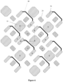
- a display unit 40 is shown in a dashed box (no real boundaries in an actual pixel structure). Consecutive display units 40 may form consecutive display unit rows along the direction of the row axis and consecutive display unit columns along the direction of the column axis. Based on the sub-pixels shared by display units, sub-pixels in a pixel structure can be divided according to a plurality of different arrangements. Figure 7 illustrates display units 40 with a plurality of different arrangements. Each of the display unit 40 may represent a different configuration/arrangement of the sub-pixels in the display unit 40 sharing sub-pixels with adjacent display units 40.
- Each display unit 40 in Figure 7 may share the first sub-pixels 10 and the third sub-pixel string 32 with adjacent display units 40.
- the position of an adjacent pixel unit 40, sharing the first sub-pixels 10 and/or the third sub-pixel string 32, may be dependent on the positions of the first sub-pixels 10 and the third sub-pixels 30 within the display unit 40.
- a third sub-pixel string 32 may include two neighboring third sub-pixels 30 along a diagonal direction.
- Each of the third sub-pixels 30 may form a third sub-pixel group 31 with another third sub-pixel 30.
- the two neighboring third sub-pixels 30 may be positioned on two sides of the second sub-pixel 20 along a diagonal direction.
- Each of the two neighboring third sub-pixels 30 may be in a row adjacent to the second sub-pixel 20 and has the shortest distance to the second sub-pixel 20 along the diagonal direction.
- two third sub-pixels 30 connected with a line may form one third sub-pixel string 32.
- a second sub-pixel 20, a third sub-pixel string 32 having a shortest distance to the second sub-pixel 20, and the two first sub-pixels 10 positioned on two sides of the second sub-pixel 20 may form a display unit 40.
- the two first sub-pixels 10 may each be in an adjacent row and each having a shortest distance to the second sub-pixel 20 along a diagonal direction.
- FIG 7 each illustrates a structure of a display unit 40.
- Each of the display units includes a third sub-pixel string 32 formed by two third sub-pixels 30 with direct connection (i.e., the third sub-pixels are directly connected).
- Direction connection refers to the connection between objects formed by direct wiring instead of being formed through algorithms and/or indirect wiring through back panel wiring.
- (B) and (E) in Figure 7 each illustrates a structure of a display unit 40 with adjacent display unit rows (i.e., the upper adjacent display unit row and/or the lower adjacent display unit row).
- Each of the third sub-pixels 30 in the display unit 40 can be directly connected to a third sub-pixel 30 of another display unit 40 in the adjacent row (i.e., the upper adjacent display unit row and/or the lower adjacent display unit row) to form a third sub-pixel string. That is, the third sub-pixel 30 may form direction connection with another display unit 40 in the adjacent row.
- the display units 40 can display the color of the third sub-pixel through the third sub-pixel string connecting the display unit 40 and the adjacent display unit 40 in the upper display unit row, or through the third sub-pixel string connecting the display unit 40 and the adjacent display unit 40 in the lower display unit row.
- the display unit 40 can also display the color of the third sub-pixel through a third sub-pixel string connecting the display unit 40 and the adjacent display units 40 in the upper display unit row and the lower display unit row simultaneously.
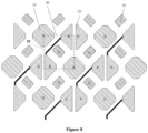
- Figure 3 illustrates a pixel structure modified from the pixel structure illustrated in Figure 1 .
- a third sub-pixel string 32 (shown by two third sub-pixels connected with a line) may refer to two adjacent third sub-pixels 30 aligned along a diagonal direction.
- the two adjacent third sub-pixels 30 may be positioned on two sides of a second sub-pixel 20 along a diagonal direction and each of the two third sub-pixels 30 is contained in a different third sub-pixel group 31 (not shown) adjacent to the second sub-pixel 20.
- One of the two adjacent third sub-pixels 30 may be positioned in the upper adjacent column and the other may be positioned in the lower adjacent column.
- Each of the two adjacent third sub-pixels 30 may have the shortest distance to the second sub-pixel 20 along the diagonal direction.
- a second sub-pixel 20, a third sub-pixel string 32 with the shortest distance to the second sub-pixel 20, and the two first sub-pixels 10 positioned in adjacent columns on two sides of the second sub-pixel 20 may form a display unit 40.
- the two first sub-pixels 10 may each have a shortest distance to the second sub-pixel 20 along the diagonal direction.
- four second sub-pixels 20 may each be adjacent to a same first sub-pixel 10 along a diagonal direction. Of the four second sub-pixels 20, two aligned along a diagonal direction may have centrosymmetry about the geometric center of the first sub-pixel 10, the other two aligned along the other diagonal direction may also have centrosymmetry about the geometric center of the first sub-pixel 10.
- the four display units 40 each including one of the second sub-pixel 20, may share the first sub-pixel 10.
- the third sub-pixel group 32 neighboring the second sub-pixel 20 may be shared by adjacent display units 40 in the upper adjacent display unit row and/or in the lower adjacent display unit row.
- the third sub-pixel string 32 neighboring the second sub-pixel 20 may be shared by adjacent display units 40 in the upper/right adjacent display unit column and/or in the lower/left adjacent display unit column.
- the four adjacent display units 40 may form a 2 by 2 block shape.
- the four adjacent display units may include five first sub-pixels 10.
- the first sub-pixel 10 positioned in the center may be adjacent to the second sub-pixel 20 of the four display unit 40 along a diagonal direction.
- two aligned along a diagonal direction may have centrosymmetry about the geometric center of the first sub-pixel 10 in the center, and the other two aligned along the other diagonal direction may also have centrosymmetry about the geometric center of the first sub-pixel 10 in the center.
- the first sub-pixel 10 may be shared by the four diaplay units 40.
- Each of the four first sub-pixels 10 positioned at the four corners of the color gamut area formed by the four display units 40 may be shared by adjacent display units 40 in the adjacent (upper and/or lower) diaplay unit rows.
- the shape of the first sub-pixel 10, the shape of the third sub-pixel group 31, and the shape of the second sub-pixel 20 may each be a symmetrical shape, e.g., have at least an axis of symmetry.
- the axis of symmetry of the shape of a first sub-pixel 10 may extend along a direction parallel to the direction of the row axis or column axis, or along a diagonal direction (as shown in Figure 1 and Figures 3 to 6 ).
- the axis of symmetry of the shape of a third sub-pixel group 31 or a third sub-pixel 30 may extend along a direction parallel to the direction of the row axis (as shown in Figure 3 ) or column axis (as shown in Figures 1 and 4 ), or along a diagonal direction (as shown in Figures 5 and 6 ).
- the axis of symmetry of the shape of a second sub-pixel 20 may extend along a direction parallel to the direction of the row axis (as shown in Figure 1 and Figures 3 to 6 , when the shape of the second sub-pixel 20 is a square, a rhombus, a circle, and/or other suitable regular polygons) or column axis (as shown in Figure 1 and Figures 3 to 6 , when the shape of the second sub-pixel 20 is a square, a rhombus, a circle, and/or other suitable polygons), or along a diagonal direction (as shown in Figure 1 and Figures 3 to 6 ).
- the overall arrangement of the first sub-pixels 10, the second sub-pixels 20, and the third sub-pixel groups 31 may form a structure/pattern with axes of symmetries.
- the FMM is often stretched along the direction of the row axis and/or column axis. Since the axes of symmetries of the pattern/structure may be parallel along the direction of row axis and/or column axis, the FMM may not be deformed during the manufacturing process. The shapes of the sub-pixels may not be distorted.
- the arrangement/designs described above may ensure the positiones of the sub-pixels in the pixel structure to remain accurate.
- the turning angles of certain shapes e.g., quadrilaterals or octagonal
- the sub-pixels e.g., the first sub-pixels 10, the second sub-pixels 20, and/or the third sub-pixel groups 31
- the turning angles of certain shapes may be chamfered to improve independent color displays between the sub-pixels.
- the overall arrangement of the first sub-pixels 10 may form lines along a diagonal direction of 45 degrees or 135 degrees with the direction of the row axis.
- the overall arrangement of the second sub-pixels 20 may form lines along a diagonal direction of 45 degrees or 135 degrees with the direction of the row axis.
- the overall arrangement of the third sub-pixel groups 31 and/or the third sub-pixels 30 may form lines along a diagonal direction of 45 degrees or 135 degrees with the direction of the row axis. That is, a second sub-pixel 20 may be positioned between two adjacent first sub-pixels 10 and between two adjacent third sub-pixel groups 31.
- Each second sub-pixel 20 may be positioned in a diagonal direction of 45 degrees with respect to an adjacent first sub-pixel 10 (or third sub-pixel group 31).
- the diagonal direction of 45 degrees may refer to the angle between the line connecting the geometric centers of the second sub-pixel 20 and an adjacent first sub-pixel 10 (or third sub-pixel group 31) and the direction of the row axis.
- the diagonal direction may refer to an angle of 45 degrees in the upper left with the direction of the row axis, an angle of 45 degrees in the upper right with the direction of the row axis, an angle of 45 degrees in the lower left with the direction of the row axis, and/or an angle of 45 degrees in the lower right with the direction of the row axis.
- the pixel structures described above may include a line of single sub-pixels (e.g., a line of only second sub-pixels 20) or a column of single sub-pixels on the edges of the pixel structures.
- a single sub-pixel may form a display unit 40 with sub-pixels in the adjacent rows or columns to display images.
- the display unit 40 may include three sub-pixels.
- the first sub-pixel 10, the third sub-pixel group 31, the third sub-pixel 30, and the second sub-pixel 20 may each have a circular shape, a triangular shape, a quadrilateral shape, a pentagonal shape, a hexagonal shape, and/or octagonal shape.
- the shape of a sub-pixel may be determined according to manufacturing/design requirements.
- the first sub-pixel 10 may have a quadrilateral shape and/or an octagonal shape
- the third sub-pixel 30 may have a triangular shape and/or a quadrilateral shape.
- Two adjacent third sub-pixels 30, facing each other, may form a third sub-pixel group 31, and the third sub-pixel group 31 may have an overall shape of a quadrilateral shape and/or an octagonal shape.
- the second sub-pixel 20 may have a quadrilateral shape and/or an octagonal shape.
- the pixel structures illustrated in Figures 3 and 4 are modified from the pixel structure of Figure 1 .
- the first sub-pixel 10 may have a rhombic shape
- the third sub-pixel 30 may have an isosceles triangle shape.
- the third sub-pixel group 31, formed by the two adjacent third sub-pixels 30 facing each other, may have an overall shape of a rhombic shape.
- the second sub-pixel 20 may have a triangle shape.
- the pixel structures of Figures 5 and 6 are modified from the pixel structure illustrated in Figure 1 .
- the first sub-pixel 10 may have a rhombic shape
- the third sub-pixel 30 may have a rectangular shape.
- the third sub-pixel group 31, formed by the two adjacent third sub-pixels 30 facing each other, may have an overall shape of a quadrilateral shape.
- the second sub-pixel 20 may have a rectangular shape.
- the area of the first sub-pixel 10 may be equal to the area of the third sub-pixel group 31, and the area of the second sub-pixel 20 may be less than the area of the first sub-pixel 10.
- the area of the third sub-pixel group 31 may be greater than the area of the first sub-pixel 10
- the area of the first sub-pixel 10 may be greater than the area of the second sub-pixel 20.
- the color displayed by the first sub-pixels 10, the color display by the second sub-pixels 20, and the color display by the third sub-pixel group 31 may be any one of red (R), blue (B), and green (G) colors such that desirable full-color images can be displayed by the pixel structure.
- the first sub-pixels 10 may display red or blue
- the second sub-pixels 20 may display green
- the third sub-pixel groups 31 may display blue or red.
- the area of a sub-pixels for displaying blue may be larger than the area of a sub-pixel for displaying red and the area of a sub-pixel for displaying green.
- a sub-pixel for displaying green may have the smallest area. That is, the area of a second sub-pixel 20 may be smaller than the areas of both a first sub-pixel 10 and a third sub-pixel group 31.
- the sub-pixels for displaying green easier to be identified by human eye, may be distributed uniformly in the directions of row axis and column axis to ensure desirable display quality along the directions of row axis and column axis.
- the first sub-pixels may display red (R)
- the second sub-pixels 20 may display green (G)
- the third sub-pixel group 31 may display blue (B).
- the sub-pixels for displaying red each may be shared by adjacent display units.
- the sub-pixels for displaying blue may be adjacent and facing each other.
- the first sub-pixels 10 may display blue (B)
- the second sub-pixels 20 may display green (G)
- the third sub-pixel groups 31 may display red (R).
- the sub-pixels for display red may be adjacent and facing each other.
- the sub-pixels for displaying blue may be shared by adjacent display units 40.
- the arrangement described above may also reduce the areas between sub-pixels, i.e., the areas with no light emission, such that the aperture ratio can be increased to about 42%. Using conventional pixel structure designs, the aperture ratios achieved would be lower.
- the aperture ratios realized are about 20-30%, 30-35%, and 37%, respectively.
- the display resolution of the pixel structure can be improved, and desirable aperture ratio can be obtained.
- the above arrangement can also improve the lifespan and display brightness of the products.
- the red (R), green (G), and blue (B) colors described above may each be the color displayed/emitted by one sub-pixel.
- the RGB colors described above may refer to the colors of the light-emitting layer of the organic electroluminescent diodes. When biased normally, the light-emitting layer may emit light with the corresponding color.
- the colors described above may refer to the colors of the CF (Color Filter) layer in the film substrate. When the backlight passes through the CF layer, the backlight is filtered by the CF and light with the corresponding color can be produced.
- a first sub-pixel 10, a third sub-pixel string 32, and a second sub-pixel 20 each may be connected with a data line for receiving pixel display information/data.
- the third sub-pixels 30 in one third sub-pixel string 32 may receive the same display information/data.
- the addressable electrode of each sub-pixel 30 in one third sub-pixel string 32 may be electrically connected.
- a first sub-pixel 10 may only be connected with one data line and may be shared by the four display units 40 and the third sub-pixel string 32 (the two third sub-pixels 30 connected with a line) may only be connected with one data line and may be shared by three display units 40, the number of data lines used in the disclosed pixel structure can be reduced.
- the back panel wiring can be easier.
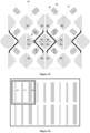
- compared to conventional pixel structures as shown in Figures 16 to 18 , when the same number of display units 40 are used in the pixel structure, fewer data lines are used in the disclosed pixel structure. Thus, the power consumption of the display apparatus containing the pixel structure can be reduced.
- the sub-pixels in the pixel structures presented above may be OLED display devices or LCD display devices. That is, the pixel structure provided by the present disclosure may be suitable for OLED display devices and LCD display devices. It is noted that, the pixel structure disclosed may also be suitable for other devices containing the pixel structures such as digital cameras, plasma display devices, and so on. For example, when the pixel structure is used in an OLED display device, the metal electrodes (i.e., anode or cathode) of each OLED, corresponding to the third sub-pixels 30 in a third sub-pixel string 32, may be electrically connected together.
- the metal electrodes i.e., anode or cathode
- each OLED may also not be connected and the same display information can be loaded on each OLED.
- the pixel electrodes of each LCD device corresponding to the third sub-pixels 30 in a third sub-pixel string 32, may be electrically connected together.
- the pixel electrode of each LCD device may also not be connected and the same display information can be loaded on each LCD device.
- the first sub-pixels 10, the second sub-pixels 20, and the third sub-pixel groups 31 may be formed through a patterning process.
- the first sub-pixels 10, the second sub-pixels 20, and the third sub-pixels 30 may be formed through a deposition process.
- the patterning process may include a photolithography process, or include a photolithography process and corresponding etching steps.
- the patterning process may also include printing, inkjet printing, and/or other process for forming predetermined patterns.
- the photolithography process may refer to the steps including film formation, exposure, and/or development. By applying appropriate photoresist films, masks, and/or exposure apparatus, patterns can be formed through the photolithography process.
- the deposition process i.e., the vacuum coating process
- the deposition process may be referred to as the process of evaporating/subliming the material/substance for forming the film and depositing the evaporated/sublimed material/substance on the surface of the substrate/device.
- the FMM can be applied on the surface of the substrate/device such that the evaporated/sublimed material/substance may not be formed in the areas covered by the FMM. Based on the pixel structure to be formed, appropriate processes can be selected to form the pattern of the pixel structure.
- the first sub-pixels 10, the second sub-pixels 20, and the third sub-pixel groups 31 may correspond to the openings in the FMM.
- the limit on the distance/spacing between two openings in the FMM may be applied on a diagonal direction (e.g., 45 degrees) to increase the density of the sub-pixels and improve the display resolution.
- the resolution of greater than 300 ppi (pixels per inch) can be obtained.
- the resolutions realized are all below 300 ppi.
- the distance between two sub-pixels may represent the distance in a diagonal direction
- the distance/spacing between two sub-pixels may be increased such that it is easier to apply the FMM to form the pattern of sub-pixels.
- the pattern may correspond to the areas on the FMM with openings to form the sub-pixels.
- the distance/spacing between the openings (i.e., along a diagonal direction) in the FMM as described above may be much greater than the distance/spacing between the openings (i.e., a long the row axis or column axis) in a conventional FMM.
- one first sub-pixel 10 can be shared by four adjacent display units 40.
- one third sub-pixel 30 when electrically connected, one third sub-pixel 30 can be shared by three display units 40 in one row or in one column.
- the distance/spacing between the openings corresponding to adjacent sub-pixels for displaying the same color (i.e., the adjacent sub-pixels for display red, blue, or green) in the FMM may be increased such that the design of the FMM and the deposition process for forming the organic layer can be easier. Higher display resolution may be easier to obtain in the pixel structures provided in the disclosure.
- the display units 40 of the pixels structures provided in the present disclosure share sub-pixels to display images.
- the manufacturing process for forming the pixel structures disclosed are greatly simplified, and the design and manufacturing of the FMM is easier.
- the present disclosure provides a new pixel structure.
- the line representing the shortest distance between the boundaries of two adjacent sub-pixels for displaying different colors may have an angle of 45 degrees with the horizontal direction.
- the arrangement of the sub-pixels described above can obtain higher display resolutions.
- the aperture ratio of the sub-pixels can be improved, and the aperture ratio of the display apparatus containing the pixel structure can be improved.
- the display brightness of the display apparatus containing the pixel structure can be improved.
- the lifespan of the OLED display device containing the pixel structure can be improved.
- the pixel structure provided in the present disclosure is suitable for forming side-by-side top-emitting AMOLED display panels through a deposition process using the FMM.
- Embodiment 2 provides the method for displaying the pixel structure in embodiment 1.
- adjacent display units 40 share one first sub-pixel 10 and one third sub-pixel string 32 for displaying images so that each display unit 40 is able to display pixel display information of three colors (i.e., the RGB colors).
- the third sub-pixels 30 on one side of the central axis of a first sub-pixel 10 and neighboring the first sub-pixel 10 may form a third sub-pixel string 32.
- the third sub-pixels 30 in the third sub-pixel string 32 may display the same color.
- One display unit 40 may include two first sub-pixel 10, a second sub-pixel 20 adjacent to the first sub-pixel 10, and a third sub-pixel string 32 neighboring/between the two first sub-pixel 10. Adjacent display units 40 may share the first sub-pixels 10 and the third sub-pixel string 32 so that each display unit 40 is able to display the pixel display information of three colors (i.e., the RGB colors).
- four adjacent display units 40 positioned in two adjacent columns of two adjacent rows, may form a 2 by 2 block shape.
- the 2 by 2 block shape may include five first sub-pixels 10.
- the first sub-pixel 10 positioned at the center of the 2 by 2 block i.e., four adjacent diaplay units 40
- the first sub-pixel 10 positioned at the center may have two perpendicular central axes and the direction of each central axis may extend between two of the four second sub-pixels 20.
- two along one diagonal direction may have mirror symmetry about a central axis of the first sub-pixel 10, and the other two along the other diagonal direction may also have mirror symmetry about a central axis of the first sub-pixel 10.
- the first sub-pixel 10 positioned at the center may be shared by the four adjacent display units 40.
- the four adjacent display units 40 may form a large color gamut area.
- the four first sub-pixels 10 positioned at the four corners of the large color gamut area i.e., each positioned at one corner) may each be shared by adjacent diaplay units 40 in the adjacent display unit rows.
- the first sub-pixels 10 may display red (R), the second sub-pixels 20 may display (G), and the third sub-pixels 30 may display blue (B).
- display units 40 with different configurations may be defined.
- the first sub-pixels 10 shared by a plurality of (e.g., four) display units 40 may be labeled as R1, R2, R3, and R4.
- the third sub-pixel strings 32 shared by a plurality of display units 40 may be labeled as B1, B2, B3, and B4.
- the sub-pixels with the same labeling number may form a color gamut (e.g., sub-pixels with labels of R1, G1, and B1 may form a gamut, and sub-pixels with labels of R2, G2, and B2 may form another color gamut).
- the colors formed by mixing the colors displayed by the sub-pixels may represent the pixel display information of the color gamut.
- a data source for providing the pixel display information may be used to input/send corresponding pixel display information (i.e., containing the RGB color information for the first sub-pixel 10, the second sub-pixel 20, and the third sub-pixel string 32), to each pixel unit 40.
- the method for displaying the pixel structure may include the following steps.
- step S1 the theoretical brightness values for each pixel unit may be obtained based on the pixel display information.
- the theoretical brightness values may correspond to the colors displayed by the first sub-pixel 10, the second sub-pixel 20, and the third sub-pixel string 32.
- the driving circuit/chip of the display panel may determine, receive, and store the pixel display information, and amplify the pixel display information for each color to obtain display information for the three primary colors (i.e., RGB colors).
- the driving circuit may further obtain brightness signals through suitable matrix transformation processes.
- the brightness signals may correspond to the theoretical brightness values of the three primary colors. The process described above can be obtained by using any suitable brightness/color separation means used in conventional manufacturing processes and is omitted herein.
- step S2 the actual brightness values of the first sub-pixel 10, the second sub-pixel 20, and the third sub-pixel string 32 of each pixel unit may be calculated.
- the actual brightness value of a first sub-pixel 10 may be calculated as a sum, i.e., a weighted sum, of the weighted theoretical brightness value of each shared portion of the first sub-pixel 10.
- the actual brightness value of a second sub-pixel 20 may be the theoretical brightness value corresponding to the color displayed by the second sub-pixel 20.
- the actual brightness value of the third sub-pixel string 32 may be calculated as a sum of the weighted theoretical brightness values of each shared portion of the third sub-pixel string 32.
- a shared portion of a first sub-pixel 10 or a third sub-pixel string 32 may refer to a portion shared by an adjacent display unit 40.
- the weight (or relative weight) for the theoretical brightness value of each shared portion of the first sub-pixel 10 may be 1/4.
- the first sub-pixels 10 may display red
- the input signal sent to a first sub-pixel 10 may be a sum of the weighted pixel display information for the red color displayed by each shared portion of the first sub-pixel 10.
- Each shared portion is shared by one of the four adjacent display units 40.
- the weight may each be 1/4.
- a third sub-pixel string 32 may include two adjacent third sub-pixels 30 along a diagonal direction. Each third sub-pixel 30 is contained in a different third sub-pixel group 31.
- a second sub-pixel 20, a third sub-pixel string 32 with the shortest distance to the second sub-pixel 20, and two first sub-pixels 10 positioned on two sides of the second sub-pixel 20 in two adjacent rows and each having the shortest distance to the second sub-pixel 20 along a diagonal direction, may form a display unit 40.
- the third sub-pixel string 32, positioned next to the second sub-pixel 20 may be shared by an adjacent display unit 40 in an upper and/or a lower adjacent display unit row.
- the third sub-pixel string 32 of one display unit 40, positioned next to the second sub-pixel 20, may be shared by an adjacent display unit 40 in an upper/right and/or a lower/left adjacent display unit column.
- the weight for the theoretical brightness value of each shared portion of a third sub-pixel 30 in the third sub-pixel string 32, shared by adjacent display units 40, may each be 1/2.
- the third sub-pixel strings 32 may display blue, and the input signal sent to the third sub-pixel string 32 may be a sum of the weighted pixel display information for the blue color of each shared portion of the third sub-pixel string 32, and the weight may each be 1/2.
- the final brightness value of a first sub-pixel 10 may be calculated as a sum of weighted theoretical brightness values for the color displayed by each shared portion of the first sub-pixels 10 (or the third sub-pixel string 31).
- the weighted theoretical brightness value is a product of the theoretical brightness value of the color displayed by a shared portion and the corresponding weight.
- the weights for theoretical brightness values of the color displayed by the first sub-pixel 10 can be adjusted to obtain a more appropriate weighted sum and improved display brightness.
- step S3 the actual brightness value may be sent/inputted to the first sub-pixel 10, the second sub-pixel 20, and the third sub-pixel string 32 of each pixel unit to display images.
- step S3 the actual brightness values of the first sub-pixel 10, the second sub-pixel 20, and the third sub-pixel string 32 of each display unit may be obtained through step S2.
- the actual brightness values may be sent to the corresponding sub-pixels to display images.
- a first sub-pixel 10, a second sub-pixel 20, and a third sub-pixel string 32 may each be connected with a data line.
- the first sub-pixel 10, the second sub-pixel 20, and the third sub-pixel string 32 may receive the corresponding actual brightness value (i.e., obtained from step S2) through the data line.
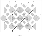
- the method for displaying the pixel structure is applied on the pixel structure illustrated in Figure 1 (in embodiment 1).
- the color mixing of a display unit, the formation of a color gamut, and the calculation of actual brightness values are illustrated for the pixel structure of Figure 9 .
- the sub-pixels for displaying red may be the first sub-pixels 10
- the sub-pixels for displaying blue may be the third sub-pixels 30, and two third sub-pixels 30 may form a third sub-pixel strings 32.
- the actual brightness values of the sub-pixels in the pixel structures of Figures 3 to 6 may be calculated in the same manner.
- the sub-pixels for displaying blue may be the first sub-pixels 10
- the sub-pixels for displaying red may be the third sub-pixels 30, and two adjacent third sub-pixels 30 may form a third sub-pixel strings 32.
- the actual brightness values of the sub-pixels in the pixel structure of Figure 8 may be calculated in the same manner and the details are omitted herein.
- brightness information of the sub-pixels can be calculated through suitable pixel sharing algorithms and desirable display effect can obtained for the pixel structure.
- the number of data lines used in the pixel structure can be reduced, and back panel wiring can be made easier.
- the power consumption of the display apparatus containing the pixel structure can be further reduced.
- the present disclosure further provides another pixel structure.
- the pixel structure may include a greater number of third sub-pixels 30 in one third sub-pixel string 32 for displaying the same color.
- Embodiment 3 provides the pixel structure. Compared to the pixel structure described in embodiment 1, the third sub-pixel strings 32 in the pixel structure provided in embodiment 3 may include more third sub-pixels 30. The third sub-pixels 30 display the same color.
- the pixel structure provided in embodiment 3 may also be used in OLED display devices and/or LCD devices.
- the pixel structure may also be used in other suitable device with display functions such as digital cameras, and plasma display devices.
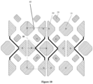
- a third sub-pixel string 32 may include three sub-pixels 30 neighboring a first sub-pixel 10.
- the three third sub-pixels 30 may be positioned on the same side of the central axis of a first sub-pixel 10.
- Each of the three third sub-pixels 30 may be contained in a different third sub-pixel group 31.
- One of the third sub-pixels 30 may be positioned at the crossing of the two diagonal directions adjacent to the first sub-pixel 10, the second third sub-pixel 30 may be aligned with the sub-pixel 30 at the crossing along one diagonal direction, and the third third sub-pixel 30 may be aligned with the sub-pixel 30 at the crossing along the other diagonal direction.
- Three consecutive second sub-pixel 20 in a column, three first sub-pixels 10 each positioned in a row between two adjacent second sub-pixels 20 and each having a shortest distance to the adjacent second sub-pixels 20 along a diagonal direction, and a third sub-pixel string 32 with a shortest distance to the second sub-pixels 20 may form a display unit 40.
- the three third sub-pixels 30 in the third sub-pixel group 32 next to the first sub-pixel 10, aligned along the two diagonal directions may include a third sub-pixel 30 adjacent to and in the same row as the first sub-pixel 10, and two adjacent third sub-pixels 30 adjacent to and in the same column on both (i.e., upper and lower) sides of the first sub-pixel 10.
- the three third sub-pixels 30 described above may each be contained in a different third sub-pixel group 31.
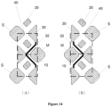
- the first sub-pixel 10 described above may be the first sub-pixel 10 marked in M in the middle row as shown in (A) and (B) of Figure 14 .
- the three third sub-pixels 30 in the third sub-pixel string 32 in the display unit 40 illustrated in Figure 10 may also be described as follows.
- the third sub-pixel string 32 may include the third sub-pixel 30 adjacent to and in the same row with the first sub-pixel 10, which is between the two first sub-pixels 10 on two sides of the display unit 40, and the two third sub-pixels 30 adjacent to and on both sides of the first sub-pixel 10, which is between the two first sub-pixels 10 on two sides of the display unit 40.
- the two third sub-pixels 30 may be contained in a different third sub-pixel group 31.
- the third sub-pixel string 32 neighboring the first sub-pixels 10 (labeled with S in (A) and (B) of Figure 14 ) on one side of a display unit 40 may represent the same third sub-pixel string 32 neighboring the other first sub-pixel 10 (labeled with M) in the same display unit 40.
- the three first sub-pixels 10 and three second sub-pixels 20 in one display unit 40 may share the same neighboring third sub-pixel string 32, as shown in (A) and (B) of Figure 14 .
- a third sub-pixel string 32 may include three sub-pixels 30 neighboring a first sub-pixel 10.
- the three third sub-pixels 30 may be positioned on the same side of the central axis of a first sub-pixel 10.
- Each of the three third sub-pixels 30 may be contained in a different third sub-pixel group 31.
- One of the third sub-pixels 30 may be positioned at the crossing of the two diagonal directions adjacent to the first sub-pixel 10, the second third sub-pixel 30 may be aligned with the sub-pixel 30 at the crossing along one diagonal direction, and the third third sub-pixel 30 may be aligned with the sub-pixel 30 at the crossing along the other diagonal direction.
- Three consecutive second sub-pixel 20 in a row, three first sub-pixels 10 each positioned in a column between two adjacent second sub-pixels 20 and each having a shortest distance to the adjacent second sub-pixels 20 along a diagonal direction, and a third sub-pixel string 32 with a shortest distance to the second sub-pixels 20 may form a display unit 40.
- the three third sub-pixels 30 in the third sub-pixel group 32, aligned along the two diagonal directions and next to the first sub-pixel 10, may include a third sub-pixel 30 adjacent to and in the same row with the first sub-pixel 10, and two third sub-pixels 30 adjacent to and in the same row on both (i.e., upper and lower) sides of the first sub-pixel 10.
- the three third sub-pixels 30 described above may each be contained in a different third sub-pixel group 31.
- the three third sub-pixels 30 in the third sub-pixel string 32 in the display unit 40 illustrated in Figure 11 may also be described as follows.
- the third sub-pixel string 32 may include the third sub-pixel 30 adjacent to and in the same column with the first sub-pixel 10, which is between the two first sub-pixels 10 on two sides of the display unit 40, and the two third sub-pixels 30 adjacent to and on both sides of the first sub-pixel 10, which is between the two first sub-pixels 10 on two sides of the display unit 40.
- the two third sub-pixels 30 may each be contained in a different third sub-pixel group 31.
- the configuration/arrangement of the second sub-pixels 20 in the pixel structure of Figure 11 can also be modified to form the pixel structure shown in Figure 12 .
- the arrangement of colors displayed by the first sub-pixels 10 and the third sub-pixels 30 in the pixel structure of Figure 11 can be modified to form the pixel structure shown in Figure 13 .
- the pixel structures of Figures 10 to 13 can be divided into different display units 40 with different configurations. Each display unit 40 may share sub-pixels with adjacent display units 40.
- Figure 14 illustrates two display units 40 (separated by the dashed line in between) with different configurations.
- three third sub-pixels 30 connected by lines may form a third sub-pixel string 32.
- Each third sub-pixel string 32 may be formed by third sub-pixels 30 with direct connection.
- the third sub-pixel string 32 may be shared by two other display units 40, and each of the two other display units 40 may include one of the two second sub-pixels 20, adjacent to the lines of direct connection, in the display unit 40.
- the two second sub-pixel 20, each adjacent to the first sub-pixel 10 in the middle (labeled with M) along a diagonal direction, may each have centrosymmetry about the geometric center of the first sub-pixel 10 (labeled with M) with another second sub-pixel 20 (not shown). That is, the two other display units 40, each containing one of the two second sub-pixels 20 in the pixel unit 40 shown in Figure 14 , may share the first sub-pixel 10 (labeled with M). Also, the two second sub-pixels 20, each adjacent to the same third sub-pixel string 32 and adjacent to the lines of direct connection in the display unit 40, may be positioned in the same column/row. The two display units 40, each containing one of the three second sub-pixels 20, may share the third sub-pixel string 32.
- the metal electrodes (i.e., anode or cathode) of the OLEDs, corresponding to the third sub-pixels 30 in a third sub-pixel string 32, are electrically connected together.
- the metal electrodes (i.e., anode or cathode) of the OLEDs may also not be connected and the same display information can be loaded on each OLED.
- the pixel electrodes corresponding to the third sub-pixels 30 in a third sub-pixel string 32 may be electrically connected together.
- the pixel electrodes may also not be connected and the same display information can be loaded on each pixel electrode.
- the pixel structure disclosed in embodiment 3 may further reduce the number of data lines used in the pixel structure.
- Back panel wiring can be made easier, and the power consumption of the display apparatus containing the pixel structure can be further reduced.
- FIG. 3 Another aspect of the present disclosure provides a method for displaying the pixel structure in embodiment 3.
- adjacent display units 40 may share a first sub-pixel 10 and a third sub-pixel string 32 for displaying images such that each display unit 40 is able to display pixel display information of three primary colors (i.e., RGB colors).
- Embodiment 4 illustrates the method for displaying the pixel structure in embodiment 3.
- the method for displaying the pixel structure disclosed in embodiment 3 can be referred to the method for displaying the pixel structure disclosed in embodiment 1. Since the number of third sub-pixels 30 in one third sub-pixel string 32 may be different from the pixel structure disclosed in embodiment 3, the weights for calculating the actual brightness values of the third sub-pixel strings 32 can be adjusted.
- a third sub-pixel string 32 may include three sub-pixels 30 next to a first sub-pixel 10.
- the three third sub-pixels 30 may be positioned on the same side of the central axis of a first sub-pixel 10.
- Each of the three third sub-pixels 30 may be contained in a different third sub-pixel group 31.
- One of the third sub-pixels 30 may be positioned at the crossing of the two diagonal directions adjacent to the first sub-pixel 10, the second third sub-pixel 30 may be aligned with the sub-pixel 30 at the crossing along one diagonal direction, and the third third sub-pixel 30 may be aligned with the sub-pixel 30 at the crossing along the other diagonal direction.
- Three consecutive second sub-pixels 20 in a column, three first sub-pixels 10 each positioned in a row between two adjacent second sub-pixels 20 and each having a shortest distance to the adjacent second sub-pixels 20 along a diagonal direction, and a third sub-pixel string 32 with a shortest distance to the second sub-pixels 20 may form a display unit 40.
- the first sub-pixels 10 may display red (R), the second sub-pixels 20 may display green (G), and the third sub-pixels 30 may display blue (B). Based on the configuration of the second sub-pixel 20 contained, different display units 40 can be defined.
- the first sub-pixel 10, which may be shared by a plurality of display units 40 may be labeled with R1, R2, R3, and R4.
- the third sub-pixel string 32, which may be shared by a plurality of display units 40, may be labeled with B1, B2, B3, and B4.
- the sub-pixels with the same labeling number may form one color gamut (e.g., R1, G1, and B1 may form one gamut, and R2, G2, and B2 may form another color gamut).
- the color formed by mixing the colors of the sub-pixels in a gamut may represent the display information of the color gamut.
- the method for displaying the pixel structure of Figure 15 may include the following steps.
- step S1 the theoretical brightness values from the pixel display information for each display unit 40 may be obtained, where the theoretical brightness values may correspond to the colors displayed by the first sub-pixel 10, the second sub-pixel 20, and the third sub-pixel string 32 of each display unit 40.
- step S2 the actual brightness values of the first sub-pixel 10, the second sub-pixel 20, and the third sub-pixel string 32 of each display unit 40 can be calculated.
- a third sub-pixel string 32 may include three sub-pixels 30 neighboring a first sub-pixel 10.
- the three third sub-pixels 30 may be positioned on the same side of the central axis of a first sub-pixel 10.
- Each of the three third sub-pixels 30 may be contained in a different third sub-pixel group 31.
- One of the third sub-pixels 30 may be positioned at the crossing of the two diagonal directions adjacent to the first sub-pixel 10, the second third sub-pixel 30 may be aligned with the sub-pixel 30 at the crossing along one diagonal direction, and the third third sub-pixel 30 may be aligned with the sub-pixel 30 at the crossing along the other diagonal direction.
- Three consecutive second sub-pixels 20 in a column, three first sub-pixels 10 each positioned in a row between two adjacent second sub-pixels 20 and each having a shortest distance to the adjacent second sub-pixels 20 along a diagonal direction, and a third sub-pixel string 32 with a shortest distance to the second sub-pixels 20 may form a display unit 40.
- the two consecutive second sub-pixels 20 may be aligned in one row/column and positioned adjacent to the third sub-pixel string 32.
- Two display units 40, each containing one of the two second sub-pixels 20, may share the same third sub-pixel string 32.
- the weights of the theoretical brightness values for the color displayed by the shared portion of the third sub-pixel string 32 in each of the three display units 40 may be 1/3.
- step S3 the corresponding actual brightness values may be inputted into the first sub-pixel 10, the second sub-pixel 20, and the third sub-pixel string 32 of each pixel unit to display images.
- brightness information of the sub-pixels can be calculated through suitable pixel sharing algorithms and the pixel structure can obtain desirable display effect.
- the number of data lines used in the pixel structure can be reduced, and back panel wiring can be easier.
- the power consumption of the display apparatus containing the pixel structure can be further reduced.
- the display apparatus may include the pixel structures disclosed in embodiment 1 or embodiment 3.
- the pixel structure in the display apparatus can be operated by the corresponding method provided in the disclosed embodiments.
- the display apparatus can be an LCD panel, an electronic paper, an OLED panel, a mobile phone, a tablet, a television, a monitor, a laptop, a digital photo frame, a navigator device, and/or any suitable product/device with display functions.
- the display apparatus since the pixel structure is formed by an improved deposition process, the aperture ratio of the sub-pixels are improved.
- the pixel structure thus has improved display brightness. Meanwhile, since the sub-pixels in the pixel structure have improved display brightness and color uniformity, the display apparatus containing the pixel structure can thus have improved display effect.
- the pixel structures and corresponding methods provided in the present disclosure improve the aperture ratio of the sub-pixels, and improve the display brightness and display resolution of the pixel structure.
- the display effect of the display apparatus containing the pixel structure can be improved.
- images can be displayed normally and back panel wiring of the data lines can be easier.
- the power consumption of the display apparatus can be reduced.
- the present disclosure provides a technical solution to the problems existing in conventional display apparatus such as difficulty in improving the display resolution in OLED display apparatuses due to limitations in manufacturing process.
Landscapes
- Engineering & Computer Science (AREA)
- Physics & Mathematics (AREA)
- General Physics & Mathematics (AREA)
- Computer Hardware Design (AREA)
- Theoretical Computer Science (AREA)
- Microelectronics & Electronic Packaging (AREA)
- Optics & Photonics (AREA)
- Geometry (AREA)
- Nonlinear Science (AREA)
- Manufacturing & Machinery (AREA)
- Mathematical Physics (AREA)
- Chemical & Material Sciences (AREA)
- Crystallography & Structural Chemistry (AREA)
- Devices For Indicating Variable Information By Combining Individual Elements (AREA)
- Electroluminescent Light Sources (AREA)
- Liquid Crystal Display Device Control (AREA)
- Control Of Indicators Other Than Cathode Ray Tubes (AREA)
- Control Of El Displays (AREA)
Claims (15)
- Pixelstruktur, die erste Subpixel (10), zweite Subpixel (20) und dritte Subpixel (30) aufweist, wobei:zwei benachbarte dritte Subpixel (30), die einander zugewandt sind, eine dritte Subpixelgruppe (31) bilden,die zweiten Subpixel (20) in einer Zeile entlang einer Richtung einer ersten Achse angeordnet sind, um zweite Subpixelzeilen zu bilden, wobei die ersten Subpixel (10) und die dritten Subpixelgruppen (31) in einer alternierenden Konfiguration entlang der Richtung der ersten Achse parallel zu den zweiten Subpixelzeilen angeordnet sind und die zweiten Subpixelzeilen und durch die ersten Subpixel (10) und die dritten Subpixelgruppen (31) gebildete Zeilen in einer alternierenden Konfiguration angeordnet sind,die zweiten Subpixel (20) entlang einer Richtung einer zweiten Achse angeordnet sind, um zweite Subpixelspalten zu bilden, die ersten Subpixel (10) und die dritten Subpixelgruppen in einer alternierenden Konfiguration entlang der Richtung der zweiten Achse parallel zu den zweiten Subpixelspalten angeordnet sind, die zweiten Subpixelspalten und durch die ersten Subpixel und die dritten Subpixelgruppen (31) gebildete Spalten in einer alternierenden Konfiguration angeordnet sind,die geometrische Mitte jedes zweiten Subpixels (20) auf einer Mittelsenkrechten einer Linie angeordnet ist, die Mittelpunkte von zwei beliebigen benachbarten dritten Subpixelgruppen (31) und ersten Subpixeln verbindet, unddie erste Achse von der zweiten Achse verschieden ist,dadurch gekennzeichnet, dassmindestens zwei dritte Subpixel (30), die in mindestens zwei verschiedenen dritten Subpixelgruppen (31) enthalten sind, durch mindestens eine direkte Verbindungslinie verbunden sind, um einen dritten Subpixelstring (32) zu bilden, wobei der dritte Subpixelstring (32) eine gleiche Farbe anzeigt, wobei jede der verschiedenen dritten Subpixelgruppen (31) ein drittes Subpixel (30) bereitstellt, das den dritten Subpixelstring (32) bildet, und wobei zwei dritte Subpixel (30), die direkt durch eine direkte Verbindungslinie verbunden sind, zwei dritte Sub-pixel (30) sind, die einander in den verschiedenen dritten Subpixelgruppen (31) am nächsten sind, undadressierbare Elektroden der dritten Subpixel (30) in einem gleichen dritten Subpixelstring (32) elektrisch verbunden sind.
- Pixelstruktur nach Anspruch 1, wobei:geometrische Mitten der ersten Subpixel in aufeinanderfolgenden Zeilen und aufeinanderfolgenden Spalten so ausgerichtet sind, dass sie Linien entlang einer von diagonalen Richtungen bilden,geometrische Mitten der dritten Subpixelgruppen in aufeinanderfolgenden Zeilen und aufeinanderfolgenden Spalten so ausgerichtet sind, dass sie Linien entlang einer diagonalen Richtung parallel zu Linien bilden, die durch die geometrischen Mitten der ersten Subpixel gebildet werden, so dass die durch die geometrischen Mitten der ersten Subpixel gebildeten Linien und durch die geometrischen Mitten der dritten Subpixelgruppen gebildete Linien in einer alternierenden Konfiguration angeordnet sind,jedes zweite Subpixel zwischen zwei benachbarten ersten Subpixeln und zwei benachbarten dritten Subpixelgruppen ausgerichtet ist, wobei die zwei benachbarten ersten Subpixel in einer diagonalen Richtung und die zwei benachbarten dritten Subpixelgruppen in einer anderen diagonalen Richtung ausgerichtet sind, undeine geometrische Mitte jedes zweiten Subpixels an einem Schnittpunkt einer Mittelsenkrechten einer Linie, die geometrische Mitten benachbarter erster Subpixel und dritter Subpixelgruppen in einer benachbarten Zeile verbindet, und einer Mittelsenkrechten einer Linie, die geometrische Mitten benachbarter erster Subpixel und einer dritten Subpixelgruppe in einer benachbarten Spalte verbindet, angeordnet ist, wobei:
eine diagonale Richtung 45 Grad im Uhrzeigersinn in Bezug auf die Richtung der Zeilenachse, 45 Grad im Gegenuhrzeigersinn in Bezug auf die Richtung der Zeilenachse, 45 Grad im Uhrzeigersinn in Bezug auf die Richtung der Spaltenachse oder 45 Grad im Gegenuhrzeigersinn in Bezug auf die Richtung der Spaltenachse beträgt. - Pixelstruktur nach Anspruch 2, wobei:geometrische Mitten der in einer Zeile oder einer Spalte angeordneten ersten Subpixel entlang einer geraden Linie ausgerichtet sind,geometrische Mitten der in einer Zeile oder einer Spalte angeordneten dritten Subpixelgruppen entlang einer geraden Linie ausgerichtet sind, undgeometrische Mitten der in einer Zeile oder einer Spalte angeordneten zweiten Subpixel entlang einer geraden Linie ausgerichtet sind, undwobei vorzugsweise eine Anzeigeeinheit das erste Subpixel, das dem ersten Subpixel benachbarte zweite Subpixel und den dem ersten Subpixel benachbarten dritten Subpixelstring aufweist, wobei benachbarte Anzeigeeinheiten das erste Subpixel und den dritten Subpixelstring gemeinsam nutzen.
- Pixelstruktur nach Anspruch 3, wobei:der dritte Subpixelstring zwei dritte Subpixel entlang einer diagonalen Richtung aufweist, jedes der beiden dritten Subpixel in einer anderen dritten Subpixelgruppe entlang der diagonalen Richtung enthalten ist und die beiden dritten Subpixel auf zwei Seiten des zweiten Subpixels in zwei benachbarten Zeilen angeordnet sind und jedes der beiden dritten Subpixel einen kürzesten Abstand zum zweiten Subpixel entlang der diagonalen Richtung hat, unddas zweite Subpixel, ein dritter Subpixelstring, der einen kürzesten Abstand zum zweiten Subpixel hat, und zwei erste Subpixel, die auf zwei Seiten des zweiten Subpixels in zwei benachbarten Zeilen angeordnet sind und jeweils einen kürzesten Abstand entlang einer diagonalen Richtung zum zweiten Sub-pixel haben, eine Anzeigeeinheit bilden,alternativ der dritte Subpixelstring zwei dritte Subpixel entlang einer diagonalen Richtung aufweist, jedes der zwei dritten Subpixel in einer anderen dritten Subpixelgruppe entlang der diagonalen Richtung enthalten ist und die zwei dritten Subpixel auf zwei Seiten des zweiten Subpixels in zwei benachbarten Spalten angeordnet sind und jedes der zwei dritten Subpixel einen kürzesten Abstand zum zweiten Subpixel entlang der diagonalen Richtung hat, unddas zweite Subpixel, ein dritter Subpixelstring mit einem kürzesten Abstand zum zweiten Subpixel und zwei erste Subpixel, die auf zwei Seiten des zweiten Subpixels in zwei benachbarten Spalten angeordnet sind und jeweils einen kürzesten Abstand entlang einer diagonalen Richtung zum zweiten Sub-pixel haben, eine Anzeigeeinheit bilden.
- Pixelstruktur nach Anspruch 4, wobei:zwei benachbarte zweite Subpixel, die auf zwei Seiten des ersten Subpixels angeordnet und entlang einer diagonalen Richtung ausgerichtet sind, eine Zentrosymmetrie um die geometrische Mitte des ersten Subpixels aufweisen, zwei weitere benachbarte zweite Subpixel, die auf zwei Seiten des ersten Sub-pixels angeordnet und entlang einer anderen diagonalen Richtung ausgerichtet sind, eine Zentrosymmetrie um die geometrische Mitte des ersten Subpixels aufweisen, und vier Anzeigeeinheiten, die jeweils eines der benachbarten zweiten Subpixel enthalten, das erste Subpixel gemeinsam nutzen, undin der Anzeigeeinheit der dritte Subpixelstring, der dem zweiten Subpixel benachbart ist, durch eine benachbarte Anzeigeeinheit in einer oberen benachbarten Zeile, eine benachbarte Anzeigeeinheit in einer unteren benachbarten Zeile oder eine Kombination davon gemeinsam genutzt wird,alternativ in der Anzeigeeinheit der dritte Subpixelstring, der dem zweiten Subpixel benachbart ist, durch eine benachbarte Anzeigeeinheit in einer oberen benachbarten Spalte, eine benachbarte Anzeigeeinheit in einer unteren benachbarten Spalte oder eine Kombination davon gemeinsam genutzt wird.
- Pixelstruktur nach Anspruch 3, wobei:der dritte Subpixelstring drei dritte Subpixel enthält, und jedes der drei dritten Subpixel in einer anderen dritten Subpixelgruppe enthalten ist,zwei der drei dritten Subpixel entlang einer diagonalen Richtung ausgerichtet sind, zwei der drei dritten Subpixel entlang der anderen diagonalen Richtung ausgerichtet sind, eines der drei dritten Subpixel auf einer Kreuzung der beiden diagonalen Richtungen angeordnet ist, unddas zweite Subpixel, zwei benachbarte erste Subpixel, die auf zwei Seiten des zweiten Subpixels in zwei benachbarten Zeilen angeordnet sind und den kürzesten Abstand zum zweiten Subpixel entlang einer diagonalen Richtung haben, und ein dritter Subpixelstring mit einem kürzesten Abstand zum zweiten Subpixel eine Anzeigeeinheit bilden.
- Pixelstruktur nach Anspruch 6, wobei der dritte Subpixelstring, der dem ersten Subpixel benachbart ist, aufweist:ein benachbartes drittes Subpixel in der gleichen Zeile wie das erste Sub-pixel und zwei benachbarte dritte Subpixel in der gleichen Spalte auf der Ober- und der Unterseite des ersten Subpixels, wobei jedes der drei benachbarten dritten Subpixel in einer anderen dritten Subpixelgruppe enthalten ist;alternativ der dritte Subpixelstring, der dem ersten Subpixel benachbart ist, aufweist:ein drittes Subpixel, das benachbart zu und in der gleichen Zeile mit einem ersten Subpixel angeordnet ist, das auf einer Seite der Anzeigeeinheit angeordnet ist, undzwei dritte Subpixel, die jeweils benachbart zu einem anderen ersten Subpixel in der gleichen Anzeigeeinheit angeordnet sind, wobei die zwei dritten Subpixel in zwei benachbarten Zeilen angeordnet und jeweils in einer anderen dritten Subpixelgruppe enthalten sind.alternativ der dritte Subpixelstring, der dem ersten Subpixel benachbart ist, aufweist:ein benachbartes drittes Subpixel in der gleichen Spalte wie das erste Subpixel und zwei benachbarte dritte Subpixel in der gleichen Zeile auf der Ober- und der Unterseite des ersten Subpixels, wobei jedes der drei benachbarten dritten Subpixel in einer anderen dritten Subpixelgruppe enthalten ist,alternativ der dritte Subpixelstring, der dem ersten Subpixel benachbart ist, aufweist:ein drittes Subpixel, das benachbart zu und in einer gleichen Spalte mit einem ersten Subpixel angeordnet ist, das auf einer Seite der Anzeigeeinheit angeordnet ist, undzwei dritte Subpixel, die jeweils benachbart zu einem anderen ersten Subpixel in einer gleichen Anzeigeeinheit angeordnet sind, wobei die zwei dritten Subpixel in zwei benachbarten Spalten angeordnet und jeweils in einer anderen dritten Subpixelgruppe enthalten sind, und/oderzwei zweite Subpixel, die dem ersten Subpixel benachbart sind und entlang einer diagonalen Richtung ausgerichtet sind, eine Zentrosymmetrie um eine geometrische Mitte des ersten Subpixels aufweisen,weitere zwei zweite Subpixel, die dem ersten Subpixel benachbart sind und entlang einer anderen diagonalen Richtung ausgerichtet sind, eine Zentrosymmetrie um die geometrische Mitte des ersten Subpixels aufweisen,vier Anzeigeeinheiten, die jeweils eines der zweiten Subpixel enthalten, das erste Subpixel gemeinsam nutzen, undzwei Anzeigeeinheiten, die jeweils eines von zwei zweiten Subpixeln enthalten, den dritten Subpixelstring gemeinsam nutzen, wobei die beiden zweiten Subpixel in einer dem dritten Subpixelstring benachbarten Zeile oder einer dem dritten Subpixelstring benachbarten Spalte ausgerichtet sind.
- Pixelstruktur nach Anspruch 2, wobei:zwei dritte Subpixel der gleichen dritten Subpixelgruppe entlang der Zeilenrichtung oder entlang der Spaltenrichtung spiegelsymmetrisch sind und zwischen zwei ersten Subpixeln angeordnet sind, undzwei dritte Subpixel, die auf zwei Seiten des gleichen ersten Subpixels und in der gleichen Zeile oder in der gleichen Spalte wie das erste Subpixel angeordnet sind, zentrosymmetrisch oder spiegelsymmetrisch um eine geometrische Mitte des ersten Subpixels sind, wobei die beiden dritten Subpixel jeweils einen kürzesten Abstand zum ersten Subpixel entlang der Richtung der Zeilenachse oder der Spaltenachse aufweisen,vorzugsweise eine Gesamtanordnung der ersten Subpixel Linien entlang einer diagonalen Richtung von 45 Grad oder 135 Grad in Bezug auf die Richtung der Zeilenachse bildet,eine Gesamtanordnung der zweiten Subpixel Linien entlang einer diagonalen Richtung von 45 Grad oder 135 Grad in Bezug auf die Richtung der Zeilenachse bildet, undeine Gesamtanordnung der dritten Subpixelgruppen Linien entlang einer diagonalen Richtung von 45 Grad oder 135 Grad in Bezug auf die Richtung der Zeilenachse bildet.
- Pixelstruktur nach Anspruch 2, wobei:zwei dritte Subpixel einer gleichen dritten Subpixelgruppe zwischen zwei benachbarten zweiten Subpixeln entlang einer diagonalen Richtung angeordnet sind und eine Linie, die geometrische Mitten der zwei dritten Subpixel verbindet, zwischen den zwei dritten Subpixeln liegt, undzwei dritte Subpixel, die dem zweiten Subpixel entlang einer diagonalen Richtung benachbart sind, eine Zentrosymmetrie oder Spiegelsymmetrie um die geometrische Mitte des zweiten Subpixels aufweisen, und/odereine Form des ersten Subpixels, eine Form der dritten Subpixelgruppe und eine Form des zweiten Subpixels jeweils eine Symmetrieachse aufweisen,die Symmetrieachse der Form des ersten Subpixels sich entlang einer Richtung parallel zur Richtung der Zeilenachse oder Spaltenachse oder entlang einer diagonalen Richtung erstreckt,die Symmetrieachse der Form der dritten Subpixelgruppe oder eines dritten Subpixels sich entlang einer Richtung parallel zur Richtung der Zeilenachse oder Spaltenachse oder entlang einer diagonalen Richtung erstreckt, unddie Symmetrieachse der Form des zweiten Subpixels sich entlang einer Richtung parallel zur Richtung der Zeilenachse oder Spaltenachse oder entlang einer diagonalen Richtung erstreckt.
- Pixelstruktur nach Anspruch 2, wobei:jede Form unter der Form eines ersten Subpixels, der Form eines zweiten Subpixels, der Form eines dritten Subpixels und der Form der dritten Subpixelgruppe eine beliebige Form unter einer kreisförmigen Form, einer dreieckigen Form, einer viereckigen Form, einer fünfeckigen Form, einer sechseckigen Form, einer achteckigen Form oder einer Kombination davon ist, und vorzugsweisedas erste Subpixel eine viereckige Form, eine achteckige Form oder eine Kombination davon hat,das dritte Subpixel eine dreieckige Form, eine viereckige Form oder eine Kombination davon hat,die dritte Subpixelgruppe, die zwei benachbarte, einander zugewandte dritte Subpixel enthält, als Gesamtform eine viereckige Form, eine achteckige Form oder eine Kombination davon aufweist, unddas zweite Subpixel eine viereckige Form, eine achteckige Form oder eine Kombination davon aufweist.
- Pixelstruktur nach Anspruch 10, wobei:das erste Subpixel eine rhombische Form hat,das dritte Subpixel eine gleichschenklige Dreiecksform hat,die dritte Subpixelgruppe, die zwei benachbarte, einander zugewandte dritte Subpixel enthält, als Gesamtform eine rhombische Form hat, unddas zweite Subpixel eine dreieckige Form hat,alternativdas erste Subpixel eine rhombische Form hat, das dritte Subpixel eine rechteckige Form hat,die dritte Subpixelgruppe, die aus zwei benachbarten, einander zugewandten dritten Subpixeln gebildet wird, als Gesamtform eine viereckige Form hat, unddas zweite Subpixel eine rechteckige Form hat.
- Pixelstruktur nach Anspruch 10, wobei:Drehwinkel der viereckigen Formen oder achteckigen Formen der ersten Subpixel, der zweiten Subpixel und der dritten Subpixelgruppen abgeschrägt sind, und/oderzwei zweite Subpixel, die einen kürzesten Abstand entlang einer Richtung der Zeilenachse oder der Spaltenachse haben, die gleichen Formen haben,alternativ zwei zweite Subpixel, die einen kürzesten Abstand entlang einer Richtung der Zeilenachse oder der Spaltenachse haben, symmetrisch um eine Mittelsenkrechte einer Linie sind, die die geometrischen Mitten der zwei zweiten Subpixel verbindet.
- Pixelstruktur nach Anspruch 1, wobei:geometrische Mitten der ersten Subpixel, geometrische Mitten der zweiten Subpixel und geometrische Mitten der dritten Subpixelgruppen gleichmäßig verteilt sind, und/odereine Fläche des ersten Subpixels einer Fläche der dritten Subpixelgruppe gleicht, und eine Fläche des zweiten Subpixels kleiner ist als die Fläche des ersten Subpixels,alternativ die Fläche der dritten Subpixelgruppe größer ist als die Fläche des ersten Subpixels, und die Fläche des ersten Subpixels größer ist als die Fläche des zweiten Subpixels, und/odereine Farbe, die durch das erste Subpixel angezeigt wird, eine Farbe, die durch das zweite Subpixel angezeigt wird, und eine Farbe, die durch die dritte Subpixelgruppe angezeigt wird, jeweils eine der Farben Rot, Grün und Blau ist, wobei vorzugsweise das erste Subpixel Rot oder Blau anzeigt, das zweite Sub-pixel Grün anzeigt, und die dritte Subpixelgruppe Blau oder Rot anzeigt.
- Pixelstruktur nach Anspruch 4, wobei:jedes Element unter dem ersten Subpixel, dem dritten Subpixelstring und dem zweiten Subpixel mit einer Datenleitung zum Empfangen von Pixelanzeigeinformation verbunden ist, unddie dritten Subpixel eines gleichen dritten Subpixelstrings die gleiche Anzeigeinformation empfangen.
- Anzeigevorrichtung, die die Pixelstruktur nach einem der Ansprüche 1 bis 14 aufweist.
Applications Claiming Priority (2)
| Application Number | Priority Date | Filing Date | Title |
|---|---|---|---|
| CN201410843256.9A CN104466007B (zh) | 2014-12-30 | 2014-12-30 | 一种像素结构及其显示方法、显示装置 |
| PCT/CN2015/089921 WO2016107218A1 (en) | 2014-12-30 | 2015-09-18 | Pixel structure and displaying method thereof, and related display apparatus |
Publications (3)
| Publication Number | Publication Date |
|---|---|
| EP3241237A1 EP3241237A1 (de) | 2017-11-08 |
| EP3241237A4 EP3241237A4 (de) | 2018-07-11 |
| EP3241237B1 true EP3241237B1 (de) | 2024-05-08 |
Family
ID=52911721
Family Applications (1)
| Application Number | Title | Priority Date | Filing Date |
|---|---|---|---|
| EP15851649.2A Active EP3241237B1 (de) | 2014-12-30 | 2015-09-18 | Pixelstruktur und anzeigeverfahren dafür sowie zugehörige anzeigevorrichtung |
Country Status (6)
| Country | Link |
|---|---|
| US (1) | US9959808B2 (de) |
| EP (1) | EP3241237B1 (de) |
| JP (1) | JP6752156B2 (de) |
| KR (1) | KR101878087B1 (de) |
| CN (1) | CN104466007B (de) |
| WO (1) | WO2016107218A1 (de) |
Families Citing this family (70)
| Publication number | Priority date | Publication date | Assignee | Title |
|---|---|---|---|---|
| US11711958B2 (en) * | 2014-09-11 | 2023-07-25 | Boe Technology Group Co., Ltd. | Display panel and display device |
| CN104465714B (zh) * | 2014-12-30 | 2017-04-26 | 京东方科技集团股份有限公司 | 一种像素结构及其显示方法、显示装置 |
| CN104466007B (zh) | 2014-12-30 | 2017-05-03 | 京东方科技集团股份有限公司 | 一种像素结构及其显示方法、显示装置 |
| CN104599625B (zh) * | 2015-03-02 | 2017-06-06 | 京东方科技集团股份有限公司 | 边界判定方法和装置、显示驱动方法和装置 |
| CA2909813A1 (en) * | 2015-10-26 | 2017-04-26 | Ignis Innovation Inc | High ppi pattern orientation |
| KR102616580B1 (ko) | 2015-11-23 | 2023-12-22 | 삼성디스플레이 주식회사 | 유기발광 디스플레이 장치 및 그 제조방법 |
| CN110137213B (zh) | 2018-02-09 | 2025-03-25 | 京东方科技集团股份有限公司 | 像素排列结构及其显示方法、显示基板 |
| US10600213B2 (en) * | 2016-02-27 | 2020-03-24 | Focal Sharp, Inc. | Method and apparatus for color-preserving spectrum reshape |
| CN105789261B (zh) | 2016-04-29 | 2018-03-06 | 京东方科技集团股份有限公司 | 像素阵列及其制造方法和有机发光二极管阵列基板 |
| KR101698718B1 (ko) * | 2016-04-29 | 2017-01-20 | 엘지디스플레이 주식회사 | 유기 발광 표시 장치 |
| CN105895663B (zh) * | 2016-05-19 | 2018-11-13 | 京东方科技集团股份有限公司 | 一种电致发光显示器件、其制作方法及显示装置 |
| CN105957488B (zh) * | 2016-07-11 | 2018-05-01 | 京东方科技集团股份有限公司 | 像素阵列及其驱动方法、显示面板及显示装置 |
| JP6842282B2 (ja) * | 2016-11-29 | 2021-03-17 | 株式会社ジャパンディスプレイ | 有機el表示装置 |
| US10367171B2 (en) * | 2016-12-29 | 2019-07-30 | Research & Business Foundation Sungkyunkwan University | Low reflective display device |
| US10264186B2 (en) * | 2017-06-30 | 2019-04-16 | Microsoft Technology Licensing, Llc | Dynamic control of camera resources in a device with multiple displays |
| CN107706213A (zh) * | 2017-09-12 | 2018-02-16 | 武汉华星光电半导体显示技术有限公司 | 一种oled显示面板及其像素排列结构 |
| US10756310B2 (en) * | 2017-09-29 | 2020-08-25 | Sharp Kabushiki Kaisha | Display device |
| CN107742638A (zh) * | 2017-11-16 | 2018-02-27 | 信利(惠州)智能显示有限公司 | 像素排列结构、有机电致发光器件和显示装置 |
| KR20190072108A (ko) * | 2017-12-15 | 2019-06-25 | 조율호 | 피라미드 서브 픽셀 배열 구조를 갖는 표시 장치 |
| CN109994508B (zh) | 2018-01-02 | 2024-09-03 | 京东方科技集团股份有限公司 | 一种像素排布结构及相关装置 |
| CN109994505B (zh) * | 2018-01-02 | 2025-04-15 | 京东方科技集团股份有限公司 | 一种像素排布结构及相关装置 |
| CN109994504A (zh) | 2018-01-02 | 2019-07-09 | 京东方科技集团股份有限公司 | 一种像素排布结构及相关装置 |
| KR20250002804A (ko) | 2018-01-16 | 2025-01-07 | 퍼시픽 라이트 앤드 홀로그램 인크. | 전자기 필드 컴퓨팅들을 이용한 3차원 디스플레이들 |
| CN110137208A (zh) * | 2018-02-09 | 2019-08-16 | 京东方科技集团股份有限公司 | 一种像素排布结构、高精度金属掩模板及显示装置 |
| CN109003999B (zh) * | 2018-06-29 | 2020-12-11 | 昆山国显光电有限公司 | 一种像素排布结构、显示面板及显示装置 |
| US10937836B2 (en) * | 2018-09-13 | 2021-03-02 | Wuhan China Star Optoelectronics Semiconductor Display Technology Co., Ltd. | Pixel arrangement structure and display device |
| KR102578096B1 (ko) * | 2018-09-21 | 2023-09-14 | 삼성전자주식회사 | 디스플레이 중 일부 영역이 시각적으로 인식되는 현상을 개선하기 위한 전자 장치 |
| US11387283B2 (en) * | 2018-09-28 | 2022-07-12 | Sharp Kabushiki Kaisha | Display device for reducing driving load of data lines |
| CN109300958B (zh) * | 2018-10-09 | 2022-04-29 | 京东方科技集团股份有限公司 | 一种像素结构、显示面板及显示装置 |
| CN109192076B (zh) * | 2018-11-02 | 2021-01-26 | 京东方科技集团股份有限公司 | 一种显示面板和显示装置 |
| CN113823240B (zh) * | 2018-12-13 | 2023-04-18 | 京东方科技集团股份有限公司 | 显示装置 |
| CN112768500B (zh) * | 2018-12-13 | 2023-10-31 | 昆山国显光电有限公司 | 像素排列结构、显示面板及显示装置 |
| CN109817685B (zh) * | 2019-02-01 | 2021-05-07 | 武汉华星光电半导体显示技术有限公司 | Oled像素结构及显示装置 |
| KR102866754B1 (ko) * | 2019-03-04 | 2025-09-30 | 삼성디스플레이 주식회사 | 표시 장치, 표시 장치의 제조장치 및 표시 장치의 제조방법 |
| CN111697025B (zh) * | 2019-03-12 | 2023-11-17 | 上海和辉光电股份有限公司 | Oled显示器件、显示面板、显示装置以及制造方法 |
| CN111969114B (zh) * | 2019-05-20 | 2022-04-12 | 京东方科技集团股份有限公司 | 显示面板、制造显示面板的方法和掩模板 |
| AU2019279939B2 (en) | 2019-07-31 | 2021-04-08 | Boe Technology Group Co., Ltd. | Display substrate and display device |
| WO2021018304A1 (zh) | 2019-07-31 | 2021-02-04 | 京东方科技集团股份有限公司 | 显示基板以及显示装置 |
| KR102913890B1 (ko) | 2019-08-05 | 2026-01-20 | 삼성디스플레이 주식회사 | 표시 장치 |
| CN110610962B (zh) * | 2019-08-20 | 2021-02-26 | 深圳市华星光电半导体显示技术有限公司 | 透明显示面板 |
| KR102927100B1 (ko) * | 2019-09-20 | 2026-02-12 | 삼성디스플레이 주식회사 | 표시 장치 |
| US11557635B2 (en) * | 2019-12-10 | 2023-01-17 | Samsung Display Co., Ltd. | Display device, mask assembly, and apparatus for manufacturing the display device |
| US12419175B2 (en) | 2019-12-10 | 2025-09-16 | Samsung Display Co., Ltd. | Display device, mask assembly, and apparatus for manufacturing display device |
| CN111341809A (zh) | 2020-03-06 | 2020-06-26 | 武汉华星光电半导体显示技术有限公司 | 显示面板及显示装置 |
| US11569302B2 (en) * | 2020-06-23 | 2023-01-31 | Chengdu Boe Optoelectronics Technology Co., Ltd. | Pixel arrangement structure and display substrate |
| CN114420722B (zh) * | 2020-09-10 | 2026-03-06 | 京东方科技集团股份有限公司 | 显示基板及显示装置 |
| US11762333B2 (en) | 2020-09-17 | 2023-09-19 | Pacific Light & Hologram, Inc. | Reconstructing objects with display zero order light suppression |
| CN112436048A (zh) * | 2020-12-01 | 2021-03-02 | 京东方科技集团股份有限公司 | 像素结构、精细金属掩膜板、显示装置和控制方法 |
| CN112563312B (zh) * | 2020-12-10 | 2022-04-26 | 合肥维信诺科技有限公司 | 像素排布结构、显示面板及掩模组件 |
| KR102899461B1 (ko) | 2021-02-05 | 2025-12-12 | 삼성디스플레이 주식회사 | 표시 장치 |
| JP7739738B2 (ja) | 2021-03-29 | 2025-09-17 | セイコーエプソン株式会社 | 光学モジュールおよび画像表示装置 |
| CN113421902B (zh) * | 2021-06-18 | 2024-07-19 | 昆山国显光电有限公司 | 像素结构及显示装置 |
| KR20230066807A (ko) * | 2021-11-08 | 2023-05-16 | 엘지디스플레이 주식회사 | 표시 장치 |
| CN115113428B (zh) * | 2022-06-28 | 2024-01-30 | 武汉华星光电半导体显示技术有限公司 | 显示面板及显示终端 |
| US12315403B2 (en) | 2023-05-12 | 2025-05-27 | Pacific Light & Hologram, Inc. | Holographically displaying three-dimensional objects |
| US12236816B2 (en) | 2023-05-12 | 2025-02-25 | Pacific Light & Hologram, Inc. | Holographically displaying live scenes including three-dimensional objects |
| US12288490B2 (en) | 2023-05-12 | 2025-04-29 | Pacific Light & Hologram, Inc. | Holographically displaying three-dimensional objects |
| US12300132B2 (en) | 2023-05-12 | 2025-05-13 | Pacific Light & Hologram, Inc. | Holographically displaying three-dimensional objects |
| US11900842B1 (en) | 2023-05-12 | 2024-02-13 | Pacific Light & Hologram, Inc. | Irregular devices |
| US12243453B2 (en) | 2023-05-12 | 2025-03-04 | Pacific Light & Hologram, Inc. | Holographically displaying three-dimensional objects |
| US12254797B2 (en) | 2023-05-12 | 2025-03-18 | Pacific Light & Hologram, Inc. | Holographically displaying live scenes including three-dimensional objects |
| US12230176B2 (en) | 2023-05-12 | 2025-02-18 | Pacific Light & Hologram, Inc. | Holographically displaying three-dimensional objects |
| US12266280B2 (en) | 2023-05-12 | 2025-04-01 | Pacific Light & Hologram, Inc. | Holographically displaying three-dimensional objects |
| US12254798B2 (en) | 2023-05-12 | 2025-03-18 | Pacific Light & Hologram, Inc. | Holographically displaying three-dimensional objects |
| US12266279B2 (en) | 2023-05-12 | 2025-04-01 | Pacific Light & Hologram, Inc. | Holographically displaying three-dimensional objects with optical devices having in-coupling and out-coupling diffractive structures |
| US12293687B2 (en) | 2023-05-12 | 2025-05-06 | Pacific Light & Hologram, Inc. | Holographically displaying live scenes including three-dimensional objects |
| US12272279B2 (en) | 2023-05-12 | 2025-04-08 | Pacific Light & Hologram, Inc. | Holographically displaying three-dimensional objects |
| US12374247B2 (en) | 2023-05-12 | 2025-07-29 | Pacific Light & Hologram, Inc. | Holographically displaying live scenes including three-dimensional objects |
| CN116758824B (zh) * | 2023-08-16 | 2023-12-08 | 长春希达电子技术有限公司 | 一种裸眼3d显示组件及显示屏 |
| US12281984B1 (en) | 2023-12-21 | 2025-04-22 | Pacific Light & Hologram, Inc. | Optical measurements |
Family Cites Families (26)
| Publication number | Priority date | Publication date | Assignee | Title |
|---|---|---|---|---|
| US7123277B2 (en) * | 2001-05-09 | 2006-10-17 | Clairvoyante, Inc. | Conversion of a sub-pixel format data to another sub-pixel data format |
| US6714206B1 (en) | 2001-12-10 | 2004-03-30 | Silicon Image | Method and system for spatial-temporal dithering for displays with overlapping pixels |
| JP4366988B2 (ja) * | 2003-05-01 | 2009-11-18 | セイコーエプソン株式会社 | 有機el装置および電子機器 |
| US7898623B2 (en) * | 2005-07-04 | 2011-03-01 | Semiconductor Energy Laboratory Co., Ltd. | Display device, electronic device and method of driving display device |
| GB2437110B (en) * | 2006-04-12 | 2009-01-28 | Cambridge Display Tech Ltd | Optoelectronic display and method of manufacturing the same |
| US7813029B2 (en) | 2007-07-31 | 2010-10-12 | Qualcomm Mems Technologies, Inc. | Devices and methods for enhancing color shift of interferometric modulators |
| US8330352B2 (en) * | 2007-11-13 | 2012-12-11 | Samsung Display Co., Ltd. | Organic light emitting diode display and method for manufacturing the same |
| US9385167B2 (en) * | 2008-10-01 | 2016-07-05 | Universal Display Corporation | OLED display architecture |
| US9041625B2 (en) * | 2010-04-21 | 2015-05-26 | Lg Display Co., Ltd. | Subpixel arrangement structure for a display device and display device |
| KR101189025B1 (ko) * | 2010-05-31 | 2012-10-08 | 삼성디스플레이 주식회사 | 유기전계발광 표시장치의 화소배열구조 |
| JP5679161B2 (ja) * | 2010-07-23 | 2015-03-04 | 株式会社ジャパンディスプレイ | 有機エレクトロルミネッセンス表示装置 |
| DE102011053000B4 (de) * | 2010-08-27 | 2017-08-17 | Lg Display Co., Ltd. | Organische elektrolumineszente Vorrichtung |
| KR101257734B1 (ko) * | 2010-09-08 | 2013-04-24 | 엘지디스플레이 주식회사 | 유기전계발광 표시장치 |
| CN102354702A (zh) * | 2011-10-31 | 2012-02-15 | 友达光电股份有限公司 | 一种有机发光显示器的像素结构 |
| KR101615332B1 (ko) * | 2012-03-06 | 2016-04-26 | 삼성디스플레이 주식회사 | 유기 발광 표시 장치의 화소 배열 구조 |
| KR102061283B1 (ko) * | 2012-09-13 | 2020-01-02 | 삼성디스플레이 주식회사 | 유기 발광 표시 장치의 화소 배열 구조 |
| KR102063973B1 (ko) * | 2012-09-12 | 2020-01-09 | 삼성디스플레이 주식회사 | 유기전계발광 표시장치 및 그의 구동방법 |
| EP3780113B1 (de) | 2012-09-13 | 2025-07-16 | Samsung Display Co., Ltd. | Pixelanordnungsstruktur einer organischen lichtemittierenden diodenanzeige |
| US9614191B2 (en) * | 2013-01-17 | 2017-04-04 | Kateeva, Inc. | High resolution organic light-emitting diode devices, displays, and related methods |
| KR102030799B1 (ko) * | 2013-03-11 | 2019-10-11 | 삼성디스플레이 주식회사 | 유기발광표시장치 |
| US9262961B2 (en) * | 2013-08-30 | 2016-02-16 | Au Optronics Corporation | Pixel arrangement of color display apparatus |
| US9337241B2 (en) * | 2014-03-19 | 2016-05-10 | Apple Inc. | Pixel patterns for organic light-emitting diode display |
| CN103901682A (zh) * | 2014-04-18 | 2014-07-02 | 深圳市华星光电技术有限公司 | 一种像素电极单元及显示面板 |
| CN104269411B (zh) * | 2014-09-11 | 2018-07-27 | 京东方科技集团股份有限公司 | 显示面板、有机发光二极管显示器和显示装置 |
| CN104465714B (zh) | 2014-12-30 | 2017-04-26 | 京东方科技集团股份有限公司 | 一种像素结构及其显示方法、显示装置 |
| CN104466007B (zh) | 2014-12-30 | 2017-05-03 | 京东方科技集团股份有限公司 | 一种像素结构及其显示方法、显示装置 |
-
2014
- 2014-12-30 CN CN201410843256.9A patent/CN104466007B/zh active Active
-
2015
- 2015-09-18 EP EP15851649.2A patent/EP3241237B1/de active Active
- 2015-09-18 KR KR1020167033650A patent/KR101878087B1/ko active Active
- 2015-09-18 US US15/032,217 patent/US9959808B2/en active Active
- 2015-09-18 JP JP2016574966A patent/JP6752156B2/ja active Active
- 2015-09-18 WO PCT/CN2015/089921 patent/WO2016107218A1/en not_active Ceased
Also Published As
| Publication number | Publication date |
|---|---|
| KR20160148686A (ko) | 2016-12-26 |
| CN104466007B (zh) | 2017-05-03 |
| US20160351116A1 (en) | 2016-12-01 |
| US9959808B2 (en) | 2018-05-01 |
| JP2018503848A (ja) | 2018-02-08 |
| EP3241237A4 (de) | 2018-07-11 |
| EP3241237A1 (de) | 2017-11-08 |
| WO2016107218A1 (en) | 2016-07-07 |
| CN104466007A (zh) | 2015-03-25 |
| JP6752156B2 (ja) | 2020-09-09 |
| KR101878087B1 (ko) | 2018-07-12 |
Similar Documents
| Publication | Publication Date | Title |
|---|---|---|
| EP3241237B1 (de) | Pixelstruktur und anzeigeverfahren dafür sowie zugehörige anzeigevorrichtung | |
| EP3241236B1 (de) | Pixelstruktur, anzeigeverfahren dafür und anzeigevorrichtung | |
| US12225799B2 (en) | Display panel and display device | |
| JP6759396B2 (ja) | ピクセル構造およびその表示方法、表示装置 | |
| US11380236B2 (en) | Sub-pixel arrangement structure, mask device, and display device | |
| US9542885B2 (en) | Pixel unit, display panel, display method and display device | |
| US20190096962A1 (en) | Pixel structure for organic light-emitting diodes, display panel and display device including the same | |
| US10504969B2 (en) | Organic light emitting diode pixel arrangement structure and display panel | |
| WO2019019604A1 (zh) | 显示基板、显示装置及其显示方法、掩模板 | |
| KR102466271B1 (ko) | 픽셀 구조체, oled 디스플레이 디바이스, 및 구동 방법 | |
| WO2019201170A1 (zh) | 像素排列结构、显示面板、掩膜版组件及蒸镀设备 | |
| CN120152559A (zh) | 像素排列结构、显示基板、显示装置 | |
| CN107086239A (zh) | 像素结构及其制备方法和显示装置 | |
| CN108321178A (zh) | 像素结构、掩膜板及显示装置 | |
| WO2019148678A1 (zh) | 有机发光二极管像素排列结构及显示面板 |
Legal Events
| Date | Code | Title | Description |
|---|---|---|---|
| STAA | Information on the status of an ep patent application or granted ep patent |
Free format text: STATUS: THE INTERNATIONAL PUBLICATION HAS BEEN MADE |
|
| PUAI | Public reference made under article 153(3) epc to a published international application that has entered the european phase |
Free format text: ORIGINAL CODE: 0009012 |
|
| STAA | Information on the status of an ep patent application or granted ep patent |
Free format text: STATUS: REQUEST FOR EXAMINATION WAS MADE |
|
| 17P | Request for examination filed |
Effective date: 20160428 |
|
| AK | Designated contracting states |
Kind code of ref document: A1 Designated state(s): AL AT BE BG CH CY CZ DE DK EE ES FI FR GB GR HR HU IE IS IT LI LT LU LV MC MK MT NL NO PL PT RO RS SE SI SK SM TR |
|
| AX | Request for extension of the european patent |
Extension state: BA ME |
|
| DAV | Request for validation of the european patent (deleted) | ||
| DAX | Request for extension of the european patent (deleted) | ||
| A4 | Supplementary search report drawn up and despatched |
Effective date: 20180613 |
|
| RIC1 | Information provided on ipc code assigned before grant |
Ipc: H01L 27/32 20060101AFI20180607BHEP |
|
| STAA | Information on the status of an ep patent application or granted ep patent |
Free format text: STATUS: EXAMINATION IS IN PROGRESS |
|
| 17Q | First examination report despatched |
Effective date: 20200304 |
|
| REG | Reference to a national code |
Ref country code: DE Ref legal event code: R079 Ref document number: 602015088659 Country of ref document: DE Free format text: PREVIOUS MAIN CLASS: H01L0027320000 Ipc: H10K0059350000 Ref country code: DE Ref legal event code: R079 Free format text: PREVIOUS MAIN CLASS: H01L0027320000 Ipc: H10K0059350000 |
|
| RIC1 | Information provided on ipc code assigned before grant |
Ipc: H10K 59/35 20230101AFI20231115BHEP |
|
| GRAP | Despatch of communication of intention to grant a patent |
Free format text: ORIGINAL CODE: EPIDOSNIGR1 |
|
| STAA | Information on the status of an ep patent application or granted ep patent |
Free format text: STATUS: GRANT OF PATENT IS INTENDED |
|
| INTG | Intention to grant announced |
Effective date: 20240115 |
|
| RAP3 | Party data changed (applicant data changed or rights of an application transferred) |
Owner name: BOE TECHNOLOGY GROUP CO., LTD. |
|
| GRAS | Grant fee paid |
Free format text: ORIGINAL CODE: EPIDOSNIGR3 |
|
| GRAA | (expected) grant |
Free format text: ORIGINAL CODE: 0009210 |
|
| STAA | Information on the status of an ep patent application or granted ep patent |
Free format text: STATUS: THE PATENT HAS BEEN GRANTED |
|
| AK | Designated contracting states |
Kind code of ref document: B1 Designated state(s): AL AT BE BG CH CY CZ DE DK EE ES FI FR GB GR HR HU IE IS IT LI LT LU LV MC MK MT NL NO PL PT RO RS SE SI SK SM TR |
|
| REG | Reference to a national code |
Ref country code: GB Ref legal event code: FG4D |
|
| REG | Reference to a national code |
Ref country code: CH Ref legal event code: EP |
|
| REG | Reference to a national code |
Ref country code: DE Ref legal event code: R096 Ref document number: 602015088659 Country of ref document: DE |
|
| REG | Reference to a national code |
Ref country code: IE Ref legal event code: FG4D |
|
| REG | Reference to a national code |
Ref country code: LT Ref legal event code: MG9D |
|
| REG | Reference to a national code |
Ref country code: NL Ref legal event code: MP Effective date: 20240508 |
|
| PG25 | Lapsed in a contracting state [announced via postgrant information from national office to epo] |
Ref country code: IS Free format text: LAPSE BECAUSE OF FAILURE TO SUBMIT A TRANSLATION OF THE DESCRIPTION OR TO PAY THE FEE WITHIN THE PRESCRIBED TIME-LIMIT Effective date: 20240908 |
|
| PG25 | Lapsed in a contracting state [announced via postgrant information from national office to epo] |
Ref country code: BG Free format text: LAPSE BECAUSE OF FAILURE TO SUBMIT A TRANSLATION OF THE DESCRIPTION OR TO PAY THE FEE WITHIN THE PRESCRIBED TIME-LIMIT Effective date: 20240508 |
|
| PG25 | Lapsed in a contracting state [announced via postgrant information from national office to epo] |
Ref country code: FI Free format text: LAPSE BECAUSE OF FAILURE TO SUBMIT A TRANSLATION OF THE DESCRIPTION OR TO PAY THE FEE WITHIN THE PRESCRIBED TIME-LIMIT Effective date: 20240508 Ref country code: HR Free format text: LAPSE BECAUSE OF FAILURE TO SUBMIT A TRANSLATION OF THE DESCRIPTION OR TO PAY THE FEE WITHIN THE PRESCRIBED TIME-LIMIT Effective date: 20240508 |
|
| PG25 | Lapsed in a contracting state [announced via postgrant information from national office to epo] |
Ref country code: GR Free format text: LAPSE BECAUSE OF FAILURE TO SUBMIT A TRANSLATION OF THE DESCRIPTION OR TO PAY THE FEE WITHIN THE PRESCRIBED TIME-LIMIT Effective date: 20240809 |
|
| PG25 | Lapsed in a contracting state [announced via postgrant information from national office to epo] |
Ref country code: PT Free format text: LAPSE BECAUSE OF FAILURE TO SUBMIT A TRANSLATION OF THE DESCRIPTION OR TO PAY THE FEE WITHIN THE PRESCRIBED TIME-LIMIT Effective date: 20240909 |
|
| REG | Reference to a national code |
Ref country code: AT Ref legal event code: MK05 Ref document number: 1686074 Country of ref document: AT Kind code of ref document: T Effective date: 20240508 |
|
| PG25 | Lapsed in a contracting state [announced via postgrant information from national office to epo] |
Ref country code: NL Free format text: LAPSE BECAUSE OF FAILURE TO SUBMIT A TRANSLATION OF THE DESCRIPTION OR TO PAY THE FEE WITHIN THE PRESCRIBED TIME-LIMIT Effective date: 20240508 |
|
| PG25 | Lapsed in a contracting state [announced via postgrant information from national office to epo] |
Ref country code: ES Free format text: LAPSE BECAUSE OF FAILURE TO SUBMIT A TRANSLATION OF THE DESCRIPTION OR TO PAY THE FEE WITHIN THE PRESCRIBED TIME-LIMIT Effective date: 20240508 |
|
| PG25 | Lapsed in a contracting state [announced via postgrant information from national office to epo] |
Ref country code: AT Free format text: LAPSE BECAUSE OF FAILURE TO SUBMIT A TRANSLATION OF THE DESCRIPTION OR TO PAY THE FEE WITHIN THE PRESCRIBED TIME-LIMIT Effective date: 20240508 |
|
| PG25 | Lapsed in a contracting state [announced via postgrant information from national office to epo] |
Ref country code: PL Free format text: LAPSE BECAUSE OF FAILURE TO SUBMIT A TRANSLATION OF THE DESCRIPTION OR TO PAY THE FEE WITHIN THE PRESCRIBED TIME-LIMIT Effective date: 20240508 |
|
| PG25 | Lapsed in a contracting state [announced via postgrant information from national office to epo] |
Ref country code: LV Free format text: LAPSE BECAUSE OF FAILURE TO SUBMIT A TRANSLATION OF THE DESCRIPTION OR TO PAY THE FEE WITHIN THE PRESCRIBED TIME-LIMIT Effective date: 20240508 |
|
| PG25 | Lapsed in a contracting state [announced via postgrant information from national office to epo] |
Ref country code: PT Free format text: LAPSE BECAUSE OF FAILURE TO SUBMIT A TRANSLATION OF THE DESCRIPTION OR TO PAY THE FEE WITHIN THE PRESCRIBED TIME-LIMIT Effective date: 20240909 Ref country code: PL Free format text: LAPSE BECAUSE OF FAILURE TO SUBMIT A TRANSLATION OF THE DESCRIPTION OR TO PAY THE FEE WITHIN THE PRESCRIBED TIME-LIMIT Effective date: 20240508 Ref country code: NO Free format text: LAPSE BECAUSE OF FAILURE TO SUBMIT A TRANSLATION OF THE DESCRIPTION OR TO PAY THE FEE WITHIN THE PRESCRIBED TIME-LIMIT Effective date: 20240808 Ref country code: NL Free format text: LAPSE BECAUSE OF FAILURE TO SUBMIT A TRANSLATION OF THE DESCRIPTION OR TO PAY THE FEE WITHIN THE PRESCRIBED TIME-LIMIT Effective date: 20240508 Ref country code: LV Free format text: LAPSE BECAUSE OF FAILURE TO SUBMIT A TRANSLATION OF THE DESCRIPTION OR TO PAY THE FEE WITHIN THE PRESCRIBED TIME-LIMIT Effective date: 20240508 Ref country code: IS Free format text: LAPSE BECAUSE OF FAILURE TO SUBMIT A TRANSLATION OF THE DESCRIPTION OR TO PAY THE FEE WITHIN THE PRESCRIBED TIME-LIMIT Effective date: 20240908 Ref country code: HR Free format text: LAPSE BECAUSE OF FAILURE TO SUBMIT A TRANSLATION OF THE DESCRIPTION OR TO PAY THE FEE WITHIN THE PRESCRIBED TIME-LIMIT Effective date: 20240508 Ref country code: GR Free format text: LAPSE BECAUSE OF FAILURE TO SUBMIT A TRANSLATION OF THE DESCRIPTION OR TO PAY THE FEE WITHIN THE PRESCRIBED TIME-LIMIT Effective date: 20240809 Ref country code: FI Free format text: LAPSE BECAUSE OF FAILURE TO SUBMIT A TRANSLATION OF THE DESCRIPTION OR TO PAY THE FEE WITHIN THE PRESCRIBED TIME-LIMIT Effective date: 20240508 Ref country code: ES Free format text: LAPSE BECAUSE OF FAILURE TO SUBMIT A TRANSLATION OF THE DESCRIPTION OR TO PAY THE FEE WITHIN THE PRESCRIBED TIME-LIMIT Effective date: 20240508 Ref country code: BG Free format text: LAPSE BECAUSE OF FAILURE TO SUBMIT A TRANSLATION OF THE DESCRIPTION OR TO PAY THE FEE WITHIN THE PRESCRIBED TIME-LIMIT Effective date: 20240508 Ref country code: AT Free format text: LAPSE BECAUSE OF FAILURE TO SUBMIT A TRANSLATION OF THE DESCRIPTION OR TO PAY THE FEE WITHIN THE PRESCRIBED TIME-LIMIT Effective date: 20240508 Ref country code: RS Free format text: LAPSE BECAUSE OF FAILURE TO SUBMIT A TRANSLATION OF THE DESCRIPTION OR TO PAY THE FEE WITHIN THE PRESCRIBED TIME-LIMIT Effective date: 20240808 |
|
| PG25 | Lapsed in a contracting state [announced via postgrant information from national office to epo] |
Ref country code: DK Free format text: LAPSE BECAUSE OF FAILURE TO SUBMIT A TRANSLATION OF THE DESCRIPTION OR TO PAY THE FEE WITHIN THE PRESCRIBED TIME-LIMIT Effective date: 20240508 |
|
| PG25 | Lapsed in a contracting state [announced via postgrant information from national office to epo] |
Ref country code: EE Free format text: LAPSE BECAUSE OF FAILURE TO SUBMIT A TRANSLATION OF THE DESCRIPTION OR TO PAY THE FEE WITHIN THE PRESCRIBED TIME-LIMIT Effective date: 20240508 |
|
| PG25 | Lapsed in a contracting state [announced via postgrant information from national office to epo] |
Ref country code: CZ Free format text: LAPSE BECAUSE OF FAILURE TO SUBMIT A TRANSLATION OF THE DESCRIPTION OR TO PAY THE FEE WITHIN THE PRESCRIBED TIME-LIMIT Effective date: 20240508 |
|
| PG25 | Lapsed in a contracting state [announced via postgrant information from national office to epo] |
Ref country code: SK Free format text: LAPSE BECAUSE OF FAILURE TO SUBMIT A TRANSLATION OF THE DESCRIPTION OR TO PAY THE FEE WITHIN THE PRESCRIBED TIME-LIMIT Effective date: 20240508 Ref country code: RO Free format text: LAPSE BECAUSE OF FAILURE TO SUBMIT A TRANSLATION OF THE DESCRIPTION OR TO PAY THE FEE WITHIN THE PRESCRIBED TIME-LIMIT Effective date: 20240508 |
|
| PG25 | Lapsed in a contracting state [announced via postgrant information from national office to epo] |
Ref country code: SM Free format text: LAPSE BECAUSE OF FAILURE TO SUBMIT A TRANSLATION OF THE DESCRIPTION OR TO PAY THE FEE WITHIN THE PRESCRIBED TIME-LIMIT Effective date: 20240508 |
|
| PG25 | Lapsed in a contracting state [announced via postgrant information from national office to epo] |
Ref country code: SM Free format text: LAPSE BECAUSE OF FAILURE TO SUBMIT A TRANSLATION OF THE DESCRIPTION OR TO PAY THE FEE WITHIN THE PRESCRIBED TIME-LIMIT Effective date: 20240508 Ref country code: SK Free format text: LAPSE BECAUSE OF FAILURE TO SUBMIT A TRANSLATION OF THE DESCRIPTION OR TO PAY THE FEE WITHIN THE PRESCRIBED TIME-LIMIT Effective date: 20240508 Ref country code: RO Free format text: LAPSE BECAUSE OF FAILURE TO SUBMIT A TRANSLATION OF THE DESCRIPTION OR TO PAY THE FEE WITHIN THE PRESCRIBED TIME-LIMIT Effective date: 20240508 Ref country code: EE Free format text: LAPSE BECAUSE OF FAILURE TO SUBMIT A TRANSLATION OF THE DESCRIPTION OR TO PAY THE FEE WITHIN THE PRESCRIBED TIME-LIMIT Effective date: 20240508 Ref country code: DK Free format text: LAPSE BECAUSE OF FAILURE TO SUBMIT A TRANSLATION OF THE DESCRIPTION OR TO PAY THE FEE WITHIN THE PRESCRIBED TIME-LIMIT Effective date: 20240508 Ref country code: CZ Free format text: LAPSE BECAUSE OF FAILURE TO SUBMIT A TRANSLATION OF THE DESCRIPTION OR TO PAY THE FEE WITHIN THE PRESCRIBED TIME-LIMIT Effective date: 20240508 |
|
| PG25 | Lapsed in a contracting state [announced via postgrant information from national office to epo] |
Ref country code: IT Free format text: LAPSE BECAUSE OF FAILURE TO SUBMIT A TRANSLATION OF THE DESCRIPTION OR TO PAY THE FEE WITHIN THE PRESCRIBED TIME-LIMIT Effective date: 20240508 |
|
| REG | Reference to a national code |
Ref country code: DE Ref legal event code: R097 Ref document number: 602015088659 Country of ref document: DE |
|
| PLBE | No opposition filed within time limit |
Free format text: ORIGINAL CODE: 0009261 |
|
| STAA | Information on the status of an ep patent application or granted ep patent |
Free format text: STATUS: NO OPPOSITION FILED WITHIN TIME LIMIT |
|
| 26N | No opposition filed |
Effective date: 20250211 |
|
| PG25 | Lapsed in a contracting state [announced via postgrant information from national office to epo] |
Ref country code: SI Free format text: LAPSE BECAUSE OF FAILURE TO SUBMIT A TRANSLATION OF THE DESCRIPTION OR TO PAY THE FEE WITHIN THE PRESCRIBED TIME-LIMIT Effective date: 20240508 Ref country code: MC Free format text: LAPSE BECAUSE OF FAILURE TO SUBMIT A TRANSLATION OF THE DESCRIPTION OR TO PAY THE FEE WITHIN THE PRESCRIBED TIME-LIMIT Effective date: 20240508 |
|
| REG | Reference to a national code |
Ref country code: CH Ref legal event code: PL |
|
| PG25 | Lapsed in a contracting state [announced via postgrant information from national office to epo] |
Ref country code: LU Free format text: LAPSE BECAUSE OF NON-PAYMENT OF DUE FEES Effective date: 20240918 |
|
| GBPC | Gb: european patent ceased through non-payment of renewal fee |
Effective date: 20240918 |
|
| PG25 | Lapsed in a contracting state [announced via postgrant information from national office to epo] |
Ref country code: GB Free format text: LAPSE BECAUSE OF NON-PAYMENT OF DUE FEES Effective date: 20240918 |
|
| REG | Reference to a national code |
Ref country code: BE Ref legal event code: MM Effective date: 20240930 |
|
| PG25 | Lapsed in a contracting state [announced via postgrant information from national office to epo] |
Ref country code: BE Free format text: LAPSE BECAUSE OF NON-PAYMENT OF DUE FEES Effective date: 20240930 |
|
| PG25 | Lapsed in a contracting state [announced via postgrant information from national office to epo] |
Ref country code: FR Free format text: LAPSE BECAUSE OF NON-PAYMENT OF DUE FEES Effective date: 20240930 |
|
| PG25 | Lapsed in a contracting state [announced via postgrant information from national office to epo] |
Ref country code: CH Free format text: LAPSE BECAUSE OF NON-PAYMENT OF DUE FEES Effective date: 20240930 |
|
| PG25 | Lapsed in a contracting state [announced via postgrant information from national office to epo] |
Ref country code: IE Free format text: LAPSE BECAUSE OF NON-PAYMENT OF DUE FEES Effective date: 20240918 |
|
| PG25 | Lapsed in a contracting state [announced via postgrant information from national office to epo] |
Ref country code: SE Free format text: LAPSE BECAUSE OF FAILURE TO SUBMIT A TRANSLATION OF THE DESCRIPTION OR TO PAY THE FEE WITHIN THE PRESCRIBED TIME-LIMIT Effective date: 20240508 |
|
| PGFP | Annual fee paid to national office [announced via postgrant information from national office to epo] |
Ref country code: DE Payment date: 20250919 Year of fee payment: 11 |
|
| PG25 | Lapsed in a contracting state [announced via postgrant information from national office to epo] |
Ref country code: CY Free format text: LAPSE BECAUSE OF FAILURE TO SUBMIT A TRANSLATION OF THE DESCRIPTION OR TO PAY THE FEE WITHIN THE PRESCRIBED TIME-LIMIT; INVALID AB INITIO Effective date: 20150918 |
|
| PG25 | Lapsed in a contracting state [announced via postgrant information from national office to epo] |
Ref country code: HU Free format text: LAPSE BECAUSE OF FAILURE TO SUBMIT A TRANSLATION OF THE DESCRIPTION OR TO PAY THE FEE WITHIN THE PRESCRIBED TIME-LIMIT; INVALID AB INITIO Effective date: 20150918 |