EP3240065A1 - Module de stockage d'électricité - Google Patents
Module de stockage d'électricité Download PDFInfo
- Publication number
- EP3240065A1 EP3240065A1 EP15872692.7A EP15872692A EP3240065A1 EP 3240065 A1 EP3240065 A1 EP 3240065A1 EP 15872692 A EP15872692 A EP 15872692A EP 3240065 A1 EP3240065 A1 EP 3240065A1
- Authority
- EP
- European Patent Office
- Prior art keywords
- voltage detection
- tier
- separator
- terminal
- electricity storage
- Prior art date
- Legal status (The legal status is an assumption and is not a legal conclusion. Google has not performed a legal analysis and makes no representation as to the accuracy of the status listed.)
- Withdrawn
Links
- 230000005611 electricity Effects 0.000 title claims abstract description 26
- 238000003860 storage Methods 0.000 title claims abstract description 26
- 238000001514 detection method Methods 0.000 claims abstract description 102
- 238000003466 welding Methods 0.000 claims abstract description 84
- 239000000758 substrate Substances 0.000 description 17
- 238000003780 insertion Methods 0.000 description 6
- 230000037431 insertion Effects 0.000 description 6
- 238000005516 engineering process Methods 0.000 description 5
- 239000002184 metal Substances 0.000 description 5
- 239000004020 conductor Substances 0.000 description 4
- 238000004519 manufacturing process Methods 0.000 description 4
- 229920003002 synthetic resin Polymers 0.000 description 4
- 239000000057 synthetic resin Substances 0.000 description 4
- 230000000994 depressogenic effect Effects 0.000 description 3
- 230000000717 retained effect Effects 0.000 description 3
- 230000000694 effects Effects 0.000 description 2
- 238000000034 method Methods 0.000 description 2
- 230000004308 accommodation Effects 0.000 description 1
- 230000015572 biosynthetic process Effects 0.000 description 1
- 239000003990 capacitor Substances 0.000 description 1
- 238000004891 communication Methods 0.000 description 1
- 238000005520 cutting process Methods 0.000 description 1
- 238000005304 joining Methods 0.000 description 1
- 239000005001 laminate film Substances 0.000 description 1
- 239000007787 solid Substances 0.000 description 1
- 239000007858 starting material Substances 0.000 description 1
Images


Classifications
-
- H—ELECTRICITY
- H01—ELECTRIC ELEMENTS
- H01M—PROCESSES OR MEANS, e.g. BATTERIES, FOR THE DIRECT CONVERSION OF CHEMICAL ENERGY INTO ELECTRICAL ENERGY
- H01M50/00—Constructional details or processes of manufacture of the non-active parts of electrochemical cells other than fuel cells, e.g. hybrid cells
- H01M50/50—Current conducting connections for cells or batteries
-
- H—ELECTRICITY
- H01—ELECTRIC ELEMENTS
- H01M—PROCESSES OR MEANS, e.g. BATTERIES, FOR THE DIRECT CONVERSION OF CHEMICAL ENERGY INTO ELECTRICAL ENERGY
- H01M50/00—Constructional details or processes of manufacture of the non-active parts of electrochemical cells other than fuel cells, e.g. hybrid cells
- H01M50/10—Primary casings; Jackets or wrappings
- H01M50/102—Primary casings; Jackets or wrappings characterised by their shape or physical structure
- H01M50/105—Pouches or flexible bags
-
- H—ELECTRICITY
- H01—ELECTRIC ELEMENTS
- H01M—PROCESSES OR MEANS, e.g. BATTERIES, FOR THE DIRECT CONVERSION OF CHEMICAL ENERGY INTO ELECTRICAL ENERGY
- H01M50/00—Constructional details or processes of manufacture of the non-active parts of electrochemical cells other than fuel cells, e.g. hybrid cells
- H01M50/10—Primary casings; Jackets or wrappings
- H01M50/172—Arrangements of electric connectors penetrating the casing
- H01M50/174—Arrangements of electric connectors penetrating the casing adapted for the shape of the cells
- H01M50/178—Arrangements of electric connectors penetrating the casing adapted for the shape of the cells for pouch or flexible bag cells
-
- H—ELECTRICITY
- H01—ELECTRIC ELEMENTS
- H01M—PROCESSES OR MEANS, e.g. BATTERIES, FOR THE DIRECT CONVERSION OF CHEMICAL ENERGY INTO ELECTRICAL ENERGY
- H01M50/00—Constructional details or processes of manufacture of the non-active parts of electrochemical cells other than fuel cells, e.g. hybrid cells
- H01M50/20—Mountings; Secondary casings or frames; Racks, modules or packs; Suspension devices; Shock absorbers; Transport or carrying devices; Holders
- H01M50/204—Racks, modules or packs for multiple batteries or multiple cells
- H01M50/207—Racks, modules or packs for multiple batteries or multiple cells characterised by their shape
- H01M50/211—Racks, modules or packs for multiple batteries or multiple cells characterised by their shape adapted for pouch cells
-
- H—ELECTRICITY
- H01—ELECTRIC ELEMENTS
- H01M—PROCESSES OR MEANS, e.g. BATTERIES, FOR THE DIRECT CONVERSION OF CHEMICAL ENERGY INTO ELECTRICAL ENERGY
- H01M50/00—Constructional details or processes of manufacture of the non-active parts of electrochemical cells other than fuel cells, e.g. hybrid cells
- H01M50/50—Current conducting connections for cells or batteries
- H01M50/502—Interconnectors for connecting terminals of adjacent batteries; Interconnectors for connecting cells outside a battery casing
- H01M50/503—Interconnectors for connecting terminals of adjacent batteries; Interconnectors for connecting cells outside a battery casing characterised by the shape of the interconnectors
-
- H—ELECTRICITY
- H01—ELECTRIC ELEMENTS
- H01M—PROCESSES OR MEANS, e.g. BATTERIES, FOR THE DIRECT CONVERSION OF CHEMICAL ENERGY INTO ELECTRICAL ENERGY
- H01M50/00—Constructional details or processes of manufacture of the non-active parts of electrochemical cells other than fuel cells, e.g. hybrid cells
- H01M50/50—Current conducting connections for cells or batteries
- H01M50/543—Terminals
- H01M50/547—Terminals characterised by the disposition of the terminals on the cells
- H01M50/548—Terminals characterised by the disposition of the terminals on the cells on opposite sides of the cell
-
- H—ELECTRICITY
- H01—ELECTRIC ELEMENTS
- H01M—PROCESSES OR MEANS, e.g. BATTERIES, FOR THE DIRECT CONVERSION OF CHEMICAL ENERGY INTO ELECTRICAL ENERGY
- H01M50/00—Constructional details or processes of manufacture of the non-active parts of electrochemical cells other than fuel cells, e.g. hybrid cells
- H01M50/50—Current conducting connections for cells or batteries
- H01M50/543—Terminals
- H01M50/552—Terminals characterised by their shape
- H01M50/553—Terminals adapted for prismatic, pouch or rectangular cells
-
- H—ELECTRICITY
- H01—ELECTRIC ELEMENTS
- H01M—PROCESSES OR MEANS, e.g. BATTERIES, FOR THE DIRECT CONVERSION OF CHEMICAL ENERGY INTO ELECTRICAL ENERGY
- H01M50/00—Constructional details or processes of manufacture of the non-active parts of electrochemical cells other than fuel cells, e.g. hybrid cells
- H01M50/50—Current conducting connections for cells or batteries
- H01M50/543—Terminals
- H01M50/564—Terminals characterised by their manufacturing process
- H01M50/566—Terminals characterised by their manufacturing process by welding, soldering or brazing
-
- H—ELECTRICITY
- H01—ELECTRIC ELEMENTS
- H01M—PROCESSES OR MEANS, e.g. BATTERIES, FOR THE DIRECT CONVERSION OF CHEMICAL ENERGY INTO ELECTRICAL ENERGY
- H01M50/00—Constructional details or processes of manufacture of the non-active parts of electrochemical cells other than fuel cells, e.g. hybrid cells
- H01M50/50—Current conducting connections for cells or batteries
- H01M50/569—Constructional details of current conducting connections for detecting conditions inside cells or batteries, e.g. details of voltage sensing terminals
-
- H—ELECTRICITY
- H01—ELECTRIC ELEMENTS
- H01M—PROCESSES OR MEANS, e.g. BATTERIES, FOR THE DIRECT CONVERSION OF CHEMICAL ENERGY INTO ELECTRICAL ENERGY
- H01M50/00—Constructional details or processes of manufacture of the non-active parts of electrochemical cells other than fuel cells, e.g. hybrid cells
- H01M50/50—Current conducting connections for cells or batteries
- H01M50/572—Means for preventing undesired use or discharge
- H01M50/574—Devices or arrangements for the interruption of current
- H01M50/583—Devices or arrangements for the interruption of current in response to current, e.g. fuses
-
- H—ELECTRICITY
- H01—ELECTRIC ELEMENTS
- H01M—PROCESSES OR MEANS, e.g. BATTERIES, FOR THE DIRECT CONVERSION OF CHEMICAL ENERGY INTO ELECTRICAL ENERGY
- H01M50/00—Constructional details or processes of manufacture of the non-active parts of electrochemical cells other than fuel cells, e.g. hybrid cells
- H01M50/50—Current conducting connections for cells or batteries
- H01M50/572—Means for preventing undesired use or discharge
- H01M50/584—Means for preventing undesired use or discharge for preventing incorrect connections inside or outside the batteries
- H01M50/588—Means for preventing undesired use or discharge for preventing incorrect connections inside or outside the batteries outside the batteries, e.g. incorrect connections of terminals or busbars
-
- H—ELECTRICITY
- H01—ELECTRIC ELEMENTS
- H01M—PROCESSES OR MEANS, e.g. BATTERIES, FOR THE DIRECT CONVERSION OF CHEMICAL ENERGY INTO ELECTRICAL ENERGY
- H01M50/00—Constructional details or processes of manufacture of the non-active parts of electrochemical cells other than fuel cells, e.g. hybrid cells
- H01M50/50—Current conducting connections for cells or batteries
- H01M50/572—Means for preventing undesired use or discharge
- H01M50/584—Means for preventing undesired use or discharge for preventing incorrect connections inside or outside the batteries
- H01M50/59—Means for preventing undesired use or discharge for preventing incorrect connections inside or outside the batteries characterised by the protection means
- H01M50/593—Spacers; Insulating plates
-
- Y—GENERAL TAGGING OF NEW TECHNOLOGICAL DEVELOPMENTS; GENERAL TAGGING OF CROSS-SECTIONAL TECHNOLOGIES SPANNING OVER SEVERAL SECTIONS OF THE IPC; TECHNICAL SUBJECTS COVERED BY FORMER USPC CROSS-REFERENCE ART COLLECTIONS [XRACs] AND DIGESTS
- Y02—TECHNOLOGIES OR APPLICATIONS FOR MITIGATION OR ADAPTATION AGAINST CLIMATE CHANGE
- Y02E—REDUCTION OF GREENHOUSE GAS [GHG] EMISSIONS, RELATED TO ENERGY GENERATION, TRANSMISSION OR DISTRIBUTION
- Y02E60/00—Enabling technologies; Technologies with a potential or indirect contribution to GHG emissions mitigation
- Y02E60/10—Energy storage using batteries
Definitions
- the technology disclosed herein relates to an electricity storage module such as a battery module.
- a battery module described in JP 2014-78366A (Patent Document 1 below) is known.
- This battery module has a structure in which a plurality of electric cells each including positive and negative lead terminals protruding outward from end portions thereof are stacked and adjacent lead terminals of opposite polarities are connected to each other, a pair of bus bars that are individually connected to those of the lead terminals connected in order that are located at opposite ends and that have mutually opposite polarities, and voltage detection terminals connected to terminal ends of voltage detection lines are individually connected for the lead terminals.
- Patent Document 1 JP 2014-78366A
- the lead terminals are each substantially L-shaped and are bent toward the other lead terminal, and the bent portions are overlapped and welded, thereby attempting to speed up the connection operation and to reduce the size of the stack.
- the operation of connecting the voltage detection terminals to the lead terminals needs to be performed separately.
- the lead terminals located at opposite ends further require the operation to connect the bus bars thereto, and thus the assembly step is still complex. Accordingly, there is a strong demand for a further improvement.
- an electricity storage module including: a plurality of electricity storage elements each including positive and negative lead terminals protruding outward from end portions thereof; a stack in which the plurality of electricity storage elements are stacked and adjacent ones of the lead terminals of opposite polarities are connected to each other; bus bars that are individually connected to those of the lead terminals connected in order that are located at opposite ends and that have mutually opposite polarities; and voltage detection terminals that are connected to terminal ends of voltage detection lines and individually connected to the electricity storage elements, wherein the lead terminals, the bus bars, and the voltage detection terminals are collectively connected by laser welding.
- This configuration allows the bus bar and the voltage detection terminal to be collectively connected to the corresponding lead terminal, so that it is possible to simplify the assembly step, thus contributing to the reduction in the manufacturing costs.
- the technology disclosed herein may have the following configuration.
- An insulating separator interposed between adjacent ones of the lead terminals is further provided, and the bus bars and the voltage detection terminals can be mounted to the separator so as to be positioned at a position that overlaps welding portions respectively provided at the lead terminals.
- the lead terminals, the bus bars, and the voltage detection terminals are held on the separator while being normally overlapped, making it possible to further smoothly perform the subsequent laser welding operation.
- the voltage detection lines and the voltage detection terminals may be connected via fuses. This configuration can prevent an excessively large current from flowing to the voltage detection lines.
- the battery module M is used for an ISG (Integrated Starter Generator), for example.
- ISG Integrated Starter Generator
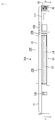
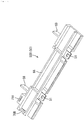
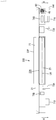
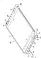
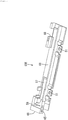
- the battery module M as a whole has the shape of a somewhat flat rectangular solid, and has a structure in which a stack 10 formed by stacking four battery units 20 shown in the drawing is accommodated in a case 80, as shown in FIG. 2 .
- the case 80 includes a case body 81 that is opened to the top and to the left side (the left front side in FIG. 2 ), a top lid 90 configured to be attached to the top surface, and a side lid 95 configured to be mounted to the left side.
- the case body 81 and the top lid 90 are made of metal, and the side lid 95 is made of synthetic resin.
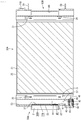
- the stack 10 will now be described. As shown in FIGS. 3 and 4 , the stack 10 is formed by stacking four battery units 20 in four tiers.
- each of the battery units 20 has a structure in which an electric cell 21 having a horizontally elongated rectangular shape in plan view is placed on a heat transfer plate 25 with separators 50 made of synthetic resin provided on the left and right side edges.
- the separators 50 on the left and right sides are each formed in the shape of a somewhat flat angular bar having a length comparable to the length of the left and right end edges (shorter-side end edges) of the heat transfer plate 25, and are each configured to be attached by inserting and locking, to a pair of insertion-type lock portions 51 provided on the inner surface thereof (the surface opposing the left and right end edges of the heat transfer plate 25), locking members 26 ( FIG. 14 ) opposingly protruding at the left and right end edges of the heat transfer plate 25, as shown in FIGS. 15 and 16 .
- each electric cell 21 is a laminated cell, which has the shape of a plane rectangle that is long in the left-right direction as described above by enveloping a power generating element (not shown) with a laminate film, and one end side thereof in the length direction serves as a positive electrode, and the other end side thereof serves as a negative electrode.
- the four electric cells 21 have oposite orientations with respect to the horizontal direction, and are stacked with the end edges of the positive electrodes and the end edges of the negative electrodes in alternation.
- a lead terminal 22 having a thin strip shape protrudes outward.
- the lead terminal 22 protruding from an end edge of the positive electrodes has an L-shape whose distal end portion is upwardly bent at a right angle
- the lead terminal 22 (negative lead terminal 22N) protruding from an end edge of each of the negative electrodes has an L-shape whose distal end portion is downwardly bent at a right angle.
- the positive lead terminal 22P has a downward L-shape.
- the lead terminals 22 are connected to each other on the right end edge side (the right back side in FIG. 4 ) for the electric cell 21 in the first tier (lowermost tier) and the electric cell 21 in the second tier, the lead terminals 22 are connected to each other on the left end edge side for the electric cell 21 in the subsequent second tier and the electric cell 21 in the third tier, and finally, the lead terminals 22 are connected to each other on the right end edge side again for the electric cell 21 in the third tier and the electric cell 21 in the fourth tier (uppermost tier).
- the negative lead terminal 22N of the electric cell 21 in the first tier and the positive lead terminal 22P of the electric cell 21 in the fourth tier are configured such that a pair of bus bars 30 (a negative bus bar 30N and a positive bus bar 30P) are respectively connected thereto.
- means for detecting the voltages of the electric cells 21 are provided. Accordingly, five voltage detection lines (not shown) are provided, and voltage detection terminals 40 connected to the terminal ends of the respective voltage detection lines are connected in a total of five locations, namely, the negative lead terminal 22N of the electric cell 21 in the first tier, the lead terminal 22 connected between the electric cells 21 in the first and second tiers, the lead terminal 22 connected between the electric cells 21 in the second and third tiers, the lead terminal 22 connected between the electric cells 21 in the third and fourth tiers, and the positive lead terminal 22P of the electric cell 21 in the fourth tier.
- the battery unit 20 in each of the tiers basically has a structure in which the electric cell 21 is placed on the heat transfer plate 25 with the insulating separators 50 provided at the left and right side edges.
- the type of the conductors (the lead terminal 22, the bus bar 30, and the voltage detection terminal 40) mounted to the separators 50 differ for the battery unit 20 in each tier, and the shapes of the separators 50 differ accordingly.
- the structure of the battery unit 20 will be described for each tier, focusing on the difference in shape between the separators 50. Note that members and portions having identical functions are denoted by identical reference numerals, and redundant descriptions thereof have been omitted or simplified.
- the battery unit 20A in the first tier (lowermost tier) will be described with reference to FIGS. 11 to 16 .
- the battery unit 20A in the first tier is configured such that the negative lead terminal 22N of the electric cell 21, the negative bus bar 30N, and the voltage detection terminal 40 are mounted to a first separator 50A attached at the left side edge of the heat transfer plate 25, whereas only the positive lead terminal 22P is mounted to a second separator 50B on the right side.
- the negative lead terminal 22N mounted to the first separator 50A on the left side has an L-shape whose distal end portion is downwardly bent, and the downward portion serves as a welding portion 23.
- the negative bus bar 30N includes an elongated substrate 31 having an standing portion 32, at a front end (the lower end in the drawing). As shown in FIG. 12 , a negative plate 35N protrudes leftward from the upper edge of the upright portion 32, and a connection hole 36 is opened at the protruding end thereof. A welding portion 37 is formed upright over a wide region on the rear end side at the right side edge of the substrate 31.
- the voltage detection terminal 40 includes an elongated substrate 41 having a widened portion 42 on the front end side.
- a connection plate 43 is formed upright from a left end portion of the front edge of the widened portion 42, and a welding portion 44 is formed upright from a rear end portion of the left side edge of the substrate 41.
- a recessed groove 53 is formed so as to open at the rear end at a position located slightly to the back from the front end (the back side in the drawing), and a platform 55 on which the negative bus bar 30N is placed bulges out at the central portion at the left side edge of the recessed groove 53.
- a recessed portion 56 to which the substrate 31 (including the upright portion 32) of the negative bus bar 30N is tightly fitted is formed in the platform 55, and the bottom of the recessed portion 56 is continuous with the bottom of the recessed groove 53 but located slightly therebelow.
- the negative plate 35N protrudes leftward from a position on the front side at the upper end of the front wall of the platform 55, as shown in FIG. 11 .
- the welding portion 37 stands upright from a position located along the left side edge of the recessed groove 53.
- a placement recessed portion 57 on which the substrate 41 of the voltage detection terminal 40 is placed so as to be tightly fitted is formed in an area extending from a front end portion of the recessed groove 53 to a part of a front wall portion 54.
- a slit 58 into which the connection plate 43 can be inserted from above is formed in the front wall portion 54.
- the welding portion 44 stands upright in alignment on the front side of the welding portion 37 of the negative bus bar 30N, as shown in FIG. 14 .
- the outer surface of the welding portion 44 of the voltage detection terminal 40 and the inner surface of the welding portion 37 of the negative bus bar 30N are located on the same plane in the front-rear direction, so that the inner surface of the welding portion 23 of the negative lead terminal 22N can overlap both of these surfaces.
- the above-described voltage detection terminal 40 is connected to the terminal end of the voltage detection line via a fuse 45.
- a connector portion 60 having a cavity 61 into which a female terminal 48 can be inserted from the outside is formed at the front end portion of the first separator 50A.
- a fuse accommodating hole 65 into which the fuse 45 can be inserted from the inside is formed in the inner surface extending from the connector portion 60 to the front wall portion 54. The back end of the fuse accommodating hole 65 is in communication with the back end of the cavity 61 and a lower position of the slit 58.
- the female terminal 48 connected to the terminal end of the voltage detection line is inserted in the cavity 61 of the connector portion 60, the female terminal 48 is locked by being retained by a lance 62. Subsequently, when the fuse 45 is inserted into the fuse accommodating hole 65, one lead plate 46 is press-fitted into a press-fitting groove 48A (see FIG. 10 ) formed on the female terminal 48, and another lead plate 46 is press-fitted and attached to a press-fitting groove 43A formed on the connection plate 43 of the voltage detection terminal 40. Consequently, the terminal end of the voltage detection line is connected to the voltage detection terminal 40 via the fuse 45.
- the second separator 50B on the right side serves to mount only the positive lead terminal 22P for the mounting of the conductors, and includes a receiving portion 66 having the shape of an angular frame formed at the central portion in the length direction, as shown in FIG. 16 .
- the positive lead terminal 22P has an L-shape whose distal end portion is bent upwardly, and the upward portion serves as the welding portion 23.
- the positive lead terminal 22P is received across the receiving portion 66 provided on the second separator 50B.
- the welding portion 23 is disposed upright from a position protruding slightly outward from the right side wall of the receiving portion 66 (see FIG. 8 ).
- a pair of contact plates 59 are formed so as to protrude by the same length.
- a battery unit 20B in the second tier will be described with reference to FIGS. 17 to 20 .
- the battery unit 20B in the second tier is configured such that only the positive lead terminal 22P of the electric cell 21 is mounted to the third separator 50C on the left side, and the negative lead terminal 22N and the voltage detection terminal 40 are mounted to the fourth separator 50D on the right side.
- the receiving portion 66 having the shape of an angular frame is formed at the central portion of the third separator 50C in the length direction.
- the positive lead terminal 22P of the electric cell 21 in the second tier is also received across the receiving portion 66, and the welding portion 23 is disposed upright from a position protruding slightly outward from the left side wall of the receiving portion 66.
- a receiving portion 67 that receives the negative lead terminal 22N is set at the central portion, in the length direction, of the fourth separator 50D on the right side.
- the receiving portion 67 has a structure formed by cutting away the right side wall of the recessed groove 53.
- the placement recessed portion 57 of the voltage detection terminal 40 (oriented to be reversed in the front-rear direction with respect to the voltage detection terminal 40 in the first tier) is formed together with the connector portion 60 and the fuse accommodating hole 65.
- the welding portion 44 stands upright from a position located along the right side edge of the recessed groove 53, as shown in FIG. 20 .
- the welding portion 23 hangs down at a position located along the right side edge of the recessed groove 53, so that the rear end portion of the welding portion 23 overlaps the outer surface of the welding portion 44 of the voltage detection terminal 40.
- the voltage detection terminal 40 is connected to the terminal end of the voltage detection line via the fuse 45 in the same manner as described above.
- a battery unit 20C in the third tier has a form in which the above-described battery unit 20B in the second tier has an opposite orientation with respect to the horizonal direction (i.e. is laterally reversed), and is configured such that the fourth separator 50D is disposed on the left side of the heat transfer plate 25, the negative lead terminal 22N of the electric cell 21 in the third tier and the voltage detection terminal 40 are mounted to the fourth separator 50D, whereas the third separator 50C is disposed on the right side of the heat transfer plate 25, and only the positive lead terminal 22P is mounted to the third separator 50C, as schematically shown in FIG. 4 .
- the battery unit 20 in the fourth tier (uppermost tier) will be described with reference to FIGS. 21 to 25 .
- the battery unit 20 in the fourth tier is configured such that the positive lead terminal 22P of the electric cell 21, the positive bus bar 30P, and the voltage detection terminal 40 in the fourth tier are mounted to the fifth separator 50E attached to the left side edge of the heat transfer plate 25, whereas the above-described fourth separator 50D is disposed on the right side, and the negative lead terminal 22N of the electric cell 21 in the fourth tier is mounted.
- the positive lead terminal 22P of the electric cell 21 in the fourth tier has a downward L-shape, or in other words, formed such that a welding portion 23X hangs down.
- the positive bus bar 30P includes, at the left side edge at the rear end (the upper end in FIG. 24 ), an elongated substrate 31 including a hanging portion 39 that is bent.
- a positive plate 35P is formed protruding leftward from the lower edge of the hanging portion 39, and a connection hole 36 is opened at the protruding end.
- a welding portion 37 is formed upright over a wide region on the front end side at the left side edge of the substrate 31.
- the voltage detection terminal 40 is disposed in the same orientation as the voltage detection terminal 40 mounted to the first separator 50A in the first tier.
- a platform 68 on which the substrate 31 of the positive bus bar 30P is placed so as to be tightly fitted is formed on the rear side (the right side in FIG. 25 ) on the top of the fifth separator 50E.
- the side wall is opened by being cut away in a little more than half of the region on the front side, and a cut-out portion 69 that allows the upper end of the hanging plate 39 of the substrate 31 of the positive bus bar 30P to be fitted and escape is formed at a position located toward the rear end of the left side edge.
- the positive plate 35P provided at the lower end of the hanging portion 39 protrudes leftward from a position that is lower than the bottom of the fifth separator 50E by a predetermined dimension, as shown in FIG. 21 .
- the placement recessed portion 57 of the voltage detection terminal 40 is formed together with the connector portion 60 and the fuse accommodating hole 65.
- the welding portion 44 stands upright in alignment on the front side of the welding portion 37 of the positive bus bar 30P, as shown in FIG. 24 .
- the outer surface of the welding portion 44 of the voltage detection terminal 40 and the outer surface of the welding portion 37 of the positive bus bar 30P are located on the same plane in the front-rear direction, so that the inner surface of the welding portion 23X of the positive lead terminal 22P in the fourth tier can overlap both of these surfaces.
- the voltage detection terminal 40 is connected to the terminal end of the voltage detection line via the fuse 45 as described above.
- the receiving portion 67 that receives the negative lead terminal 22N is set at the central portion, in the length direction, of the fourth separator 50D on the right side, and the placement recessed portion 57 of the voltage detection terminal 40 is formed on the rear end side, together with the connector portion 60 and the fuse accommodating hole 65.
- the welding portion 44 rises from a position located along the right side edge of the recessed groove 53 as shown in FIG. 24 .
- the welding portion 23 hangs down at a position located along the right side edge of the recessed groove 53, so that the rear end portion of the welding portion 23 overlaps the outer surface of the welding portion 44 of the voltage detection terminal 40.
- the voltage detection terminal 40 is also connected to the terminal end of the voltage detection line via the fuse 45.
- the separators 50 on the left side and the separators 50 on the right side in four tiers are configured to be coupled to each other via a total of three types of locking portions 70, 72, and 74, namely, a first locking portion 70 composed of a first locking piece 71A and a first locking hole 71B, a second locking portion 72 composed of a second locking piece 73A and a second locking hole 73B, and a third locking portion 74 composed of a third locking piece 75A and a third locking hole 75B.
- the first locking portions 70 is set in three locations on each of the front end side for the separators 50 on the left side, and the rear end side for the separators 50 on the right side. More specifically, the first locking hole 71B is formed in the separator 50 in the first tier, the first locking hole 71B and the first locking piece 71A are formed in the separators 50 in the second tier and the third tier so as to be vertically aligned, and the first locking piece 71A is formed on the separator 50E in the fourth tier.
- the second locking portion 72 is set in three locations on each of the rear end side for the separator 50 on the left side, and the front end side for the separator 50 on the right side. More specifically, the second locking hole 73B is formed in the separator 50 in the first tier, the second locking piece 73A and the second locking hole 73B are formed in the separators 50 in the second tier and the third tier so as to be vertically aligned, and the second locking piece 73A is formed on the separator 50 in the fourth tier.
- the third locking portion 74 is set in one location between the front end faces of the separators 50 in the second tier and the third tier on the left side as shown in FIG. 4 , and two locations between the rear end faces of the separators 50 in the first tier and the second tier, and between the rear end faces of the separators 50 in the third tier and the fourth tier on the right side as shown in FIG. 10 .
- the third locking hole 75B is formed in the separator 50 in the lower tier
- the third locking piece 75A is formed on the separator 50 in the upper tier.
- an insulating member 12 that covers and insulates the lead terminals 22 exposed on the right surface of the stack 10 is provided.
- the insulating member 12 is made of synthetic resin, and has a structure in which a top plate 14 is formed protruding so as to cover the central portion on the top of the separator 50 in the fourth tie from the upper edge of the substrate 13 that covers the central portion in the width direction (the placement region of the lead terminals 22) of the separators 50 in the four tiers on the right side (separator group 50R: see FIG. 3 ) that are coupled so as to overlap one another.
- Clamping pieces 15 configured to be put against a right side edge portion on the bottom of the separator 50 in the first tier protrude at the lower edge of the substrate 13.
- a pair of attachment pieces 16 protrude from the front and rear side edges of the inner surface (the surface opposing the separator group 50R on the right side) of the substrate 13, and a pair of attachment holes 77 into which the aforementioned attachment pieces 16 are inserted and locked are formed in the right surface of the separator 50C in the third tier so as to oppose each other (see FIG. 20 ).
- the insulating member 12 When the insulating member 12 is attached to the right surface after the separators 50 in the four tiers on the right side have been normally overlapped and coupled, the insulating member 12 is retained and mounted by engagement between the attachment pieces 16 and the attachment holes 77 in a state in which the separator group 50R on the right side is clamped between the top plate 14 and the clamping pieces 15. Consequently, the lead terminals 22 exposed on the right side surface of the stack 10 are insulated from a right side plate 82A of the case body 81.
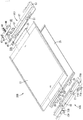
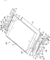
- the case 80 includes the case body 81 and the top lid 90, both of which are formed by press working a metal plate, and the side lid 95 made of synthetic resin.
- the case body 81 has the shape of a somewhat flat box that is open to the top and to the left side to accommodate the above-described stack 10.
- a raised portion 83 having a substantially rectangular shape in plan view is formed at the central portion on the bottom of the case body 81.
- a lead-out hole 84 from which the voltage detection lines pulled out to the right surface side of the stack 10 are led to the outside is formed at a rear end position of the upper edge of the right side plate 82A.
- the top lid 90 is attached to the top opening of the case body 81 described above, and a depressed portion 91 having a substantially rectangular shape in plan view is formed at the central portion of the top lid 90 so as to oppose the raised portion 83 on the bottom surface of the case body 81.
- Downward mounting plates 92 are formed at the front and rear edges and the right side edge of the top lid 90, and the top lid 90 covers the top opening of the case body 81 by the mounting plates 92 being attached to upper edge portions of front and rear plates 82B and 82C and the right side plate 82A of the case body 81 described above.
- Insertion pieces (not shown) configured to be inserted into insertion grooves 85 formed in an upper edge portion of the rear plate 82C of the case body 81 are formed on the mounting plate 92 on the rear side, and screw insertion holes 93 aligned with screw holes 86 formed in an upper edge portion of the front plate 82B of the case body 81 are formed in the mounting plate 92 on the front side.
- the side lid 95 has a rectangular shape to close the left opening of the case body 81.
- a pair of front and rear terminal blocks 97 that respectively allow insertion of and receive the negative plate 35N of the negative bus bar 30N and the positive plate 35P of the positive bus bar 30P that protrude from the left side of the stack 10 are formed on the outer surface of the side lid 95.
- a lead-out hole 98 from which the voltage detection lines pulled out to the left side of the stack 10 are led to the outside is cut out at a front end position at the lower edge of the side lid 95.
- An insulating wall 99 that insulates the positive plate 35P and the negative plate 35N if a metal plate falls on these electrodes is provided so as to protrude at a position between the two terminal blocks 97 on the outer surface of the side lid 95.
- a pair of inwardly protruding front and rear locking pawls 100 are formed at each of the upper and lower edges of the side lid 95.
- the locking pawls 100 on the upper side can enter the bottom surface of the left side edge of the top lid 90 and be locked to locking grooves 94 formed along the left side edge, whereas the locking pawls 100 on the lower side can enter the top at the left side edge of the bottom of the case body 81 and be locked to locking grooves 87 formed along the left side edge.
- the battery unit 20 is formed for each tier.
- the negative bus bar 30N and the voltage detection terminal 40 are mounted to the first separator 50A, and the fuse 45 is mounted and connected to the voltage detection terminal 40.
- the first separator 50A is attached to the left side edge of the heat transfer plate 25, and the second separator 50B in an empty state is attached to the right side edge thereof.
- the electric cell 21 is placed in a predetermined orientation on the heat transfer plate 25. At this time, as shown in FIG.
- the downwardly bent welding portion 23 of the negative lead terminal 22N of the electric cell 21 is overlapped with the outer surfaces of the welding portion 44 of the voltage detection terminal 40 and the welding portion 37 of the negative bus bar 30N that are disposed in alignment in the front-rear direction.
- the positive lead terminal 22P is received by the second separator 50B, and the upwardly bent welding portion 23 thereof is disposed standing upright at a position located substantially along the right side surface of the second separator 50B (see FIG. 11 ).
- the voltage detection terminal 40 and the fuse 45 are mounted to the fourth separator 50D on the right side.
- the fourth separator 50D is attached to the right side edge of the heat transfer plate 25, and the third separator 50C in an empty state is attached to the left side edge thereof.
- the electric cell 21 is placed in a predetermined orientation on the heat transfer plate 25, the positive lead terminal 22P of the electric cell 21 is received by the third separator 50C, and the upwardly bent welding portion 23 thereof is disposed standing upright at a position located substantially along the left side of the third separator 50C, as shown in FIG. 17 .
- the downwardly bent welding portion 23 of the negative lead terminal 22N is overlapped with the outer surface of the welding portion 44 of the voltage detection terminal 40.
- the battery unit 20C in the third tier is applied in a configuration in which the battery unit 20B in the second tier assembled in the above-described manner has an opposite orientation with respect to the horizonal direction (i.e. is laterally reversed).
- the positive bus bar 30P, the voltage detection terminal 40, and the fuse 45 are mounted to the fifth separator 50E, and the voltage detection terminal 40 and the fuse 45 are mounted to the fourth separator 50D.
- the fifth separator 50E is attached to the left side edge of the heat transfer plate 25, and the fourth separator 50D is attached to the right side edge thereof. Then, the electric cell 21 is placed in a predetermined orientation on the heat transfer plate 25. At this time, as shown in FIG.
- the downwardly bent welding portion 23X of the positive lead terminal 22P of the electric cell 21 is overlapped with the outer surfaces of the welding portion 44 of the voltage detection terminal 40 and the welding portion 37 of the negative bus bar 30N that are disposed in alignment in the front-rear direction.
- the downwardly bent welding portion 23 of the negative lead terminal 22N is overlapped with the outer surface of the welding portion 44 of the voltage detection terminal 40.
- the battery units 20 in the respective tiers When the battery units 20 in the respective tiers have been formed in the above-described manner, the battery units 20 are disposed as shown in FIG. 4 and stacked in the up-down direction. Specifically, the electric cells 21 in the respective tiers are overlapped with one another with the heat transfer plate 25 interposed therebetween, and the separators 50 in the respective tiers are overlapped with one another on the left and right sides, and are coupled via the first to third locking portions 70, 72, and 74. That is, the battery units 20 in four tiers are stacked and coupled ( FIG. 3 ).
- the upward welding portion 23 of the positive lead terminal 22P of the electric cell 21 in the first tier overlaps the outer surface of the downward welding portion 23 of the negative lead terminal 22N of the electric cell 21 in the second tier.
- the upward welding portion 23 of the positive lead terminal 22P of the electric cell 21 in the second tier overlaps the outer surface of the downward welding portion 23 of the negative lead terminal 22N of the electric cell 21 in the third tier.
- the upward welding portion 23 of the positive lead terminal 22P of the electric cell 21 in the third tier overlaps the outer surface of the downward welding portion 23 of the negative lead terminal 22N of the electric cell 21 in the fourth tier.
- the lead terminals 22, the voltage detection terminal 40, and optionally the bus bar 30, are connected by laser welding for each tier.
- the welding portion 44 of the voltage detection terminal 40 and the welding portion 37 of the negative bus bar 30N overlap, in alignment in the front-rear direction, the inner surface of the welding portion 23 of the negative lead terminal 22N of the electric cell 21 in the first tier. Accordingly, by applying laser light so as to run in the front-rear direction toward the welding portion 23 of the negative lead terminal 22N (see a laser welding portion LW shown in FIG. 13 ), the welding portion 44 of the voltage detection terminal 40 and the welding portion 37 of the negative bus bar 30N are welded in alignment to the inner surface of the welding portion 23 of the negative lead terminal 22N. As a result, the voltage detection terminal 40 and the negative bus bar 30N are collectively connected electrically to the negative lead terminal 22N of the electric cell 21 in the first tier.
- the welding portion 23 of the negative lead terminal 22N of the electric cell 21 in the second tier overlaps the inner surface of the welding portion 23 of the positive lead terminal 22P of the electric cell 21 in the first tier, and the welding portion 44 of the voltage detection terminal 40 further overlaps the inner surface thereof. Accordingly, by similarly applying laser light so as to run in the front-rear direction toward the welding portion 23 of the positive lead terminal 22P (see a laser welding portion LW in FIG. 19 ), the welding portions 23 of the positive lead terminal 22P and the negative lead terminal 22N are welded to each other, and the welding portion 44 of the voltage detection terminal 40 is also welded. As a result, the positive lead terminal 22P of the electric cell 21 in the first tier, the negative lead terminal 22N of the electric cell 21 in the second tier, and the voltage detection terminals 40 are collectively connected electrically.
- the positive lead terminal 22P of the electric cell 21 in the tier one tier lower than each of these tiers, the negative lead terminal 22N of the electric cell 21 in each of these tiers, and the voltage detection terminal 40 are collectively connected electrically.
- the welding portion 44 of the voltage detection terminal 40 and the welding portion 37 of the positive bus bar 30P overlap, in alignment in the front-rear direction, the inner surface of the downward welding portion 23X of the positive lead terminal 22P of the electric cell 21 in the fourth tier. Accordingly, by similarly performing laser welding, the voltage detection terminal 40 and the positive bus bar 30P are collectively connected electrically to positive lead terminal 22P of the electric cell 21 in the fourth tier.
- the female terminals 48 connected to the terminal ends of the five voltage detection lines that had been prepared are finally inserted and retained in the cavities 61 of the corresponding connector portions 60 provided in the separators 50, and at that time, also connected to the fuses 45 disposed in the back.
- the stack 10 is formed as shown in FIG. 3 .
- the voltage detection lines may be connected to the fuses 45 before completion of laser welding.
- the electric cells 21 stacked in four tiers are connected in series by the positive lead terminal 22P and the negative lead terminal 22N that are adjacent to each other being sequentially connected.
- the negative bus bar 30N and the positive bus bar 30P are respectively connected to the negative lead terminal 22N and the positive lead terminal 22P located at opposite ends, and are disposed in alignment in the front-rear direction so as to protrude from the left side of the stack 10.
- the voltage detection terminals 40 connected via the fuses 45 to the terminal ends of the five voltage detection lines for detecting the voltages of the electric cells 21 are respectively connected in a total of five locations, namely, at the negative lead terminal 22N of the electric cell 21 in the first tier, the lead terminal 22 connected between the electric cells 21 in the first and second tiers, the lead terminal 22 connected between the electric cells 21 in the second and third tiers, the lead terminal 22 connected between the electric cells 21 in the third and fourth tiers, and the positive lead terminal 22P of the electric cell 21 in the fourth tier.
- three voltage detection lines are pulled out leftward from a front edge portion of the left side of the stack 10, and the remaining two voltage detection lines are pulled out rightward from a rear end portion of the right side surface of the stack 10.
- the assembled stack 10 is accommodated in the case 80.
- the insulating member 12 Prior to accommodation, the insulating member 12 is mounted to the right side surface of a group of the separators 50 in four tiers on the right side of the stack 10, thus insulating and protecting the lead terminals 22 exposed on the right side surface.
- the stack 10 to which the insulating member 12 has been mounted in this manner is placed into the case body 81, as shown in FIG. 2 .
- the two voltage detection lines pulled out from the rear edge portion of the right side surface of the stack 10 are led to the outside through the lead-out hole 84 formed in the rear end of the upper edge of the right side plate 82A of the case body 81.
- the stack 10 is placed on the bottom surface of the case body 81 while being positioned with the contact plates 59 protruding on the right side of the second separator 50B in the first tier being in contact with the right side plate 82A, and the raised portion 83 is brought into contact with the heat transfer plate 25 in the first tier.
- the top lid 90 is attached to the top opening of the case body 81.
- the top lid 90 is placed on the top opening while the insertion pieces provided on the mounting plate 92 on the rear side are inserted into the insertion grooves 85 at the upper edge portion of the rear plate 82C, and is fixed by fastening, with screws 101, the mounting plate 92 on the front side and the front plate 82B in three locations. Consequently, the depressed portion 91 is pressed against the top of the electric cell 21 in the fourth tier, and the electric cells 21 and the heat transfer plates 25 that are overlapped in four tiers are clamped between the depressed portion 91 and the raised portion 83. With such a structure, the heat generated from the electrics cell 21 is transmitted to the case body 81 and the top lid 90, providing the function of releasing the heat to the outside.
- the top lid 90 When the top lid 90 is attached to the case body 81, a metal box that is open on the left surface side is formed, and finally, the side lid 95 is attached to the opening on the left surface side.
- the side lid 95 is placed toward the opening by holding the insulating wall 99 from a state in which the three voltage detection lines pulled out from the front edge portion of the left side of the stack 10 are fitted to the lead-out hole 98 at the lower edge of the front end.
- the side lid 95 is pushed in while causing the insulating plate 96 to slide onto the bottom surface of the left side edge of the top lid 90.
- the distal ends of the negative plate 35N of the negative bus bar 30N and the positive plate 35P of the positive bus bar 30P that protrude from the left side of the stack 10 face the terminal blocks 97, and the pairs of upper and lower locking pawls 100 enter the inside of the upper edge and the lower edge, respectively, of the opening.
- the pushing is stopped when the side lid 95 has come into contact with the platform 55 protruding from the left side of the first separator 50A in the first tier, and at that time, the upper and lower locking pawls 100 are fitted to the corresponding upper and lower locking grooves 94 and 87, thus retaining and attaching the side lid 95.
- the insulating plate 96 covers the top of the positive lead terminal 22P of the electric cell 21 in the fourth tier to protect the positive lead terminal 22P in the insulating state between the insulating plate 96 and the top lid 90, and the negative plate 35N and the positive plate 35P protrude onto the front and rear terminal blocks 97 by a predetermined amount.
- the three voltage detection lines are led out from the lead-out hole 98.
- connection terminals provided at the terminal end of a power line are connected by bolting on the terminal blocks 97, and the lead-out end sides of the voltage detection lines are connected to a voltage detection portion of a control unit via connectors or the like.
- the lead terminals 22, the bus bars 30, and the voltage detection terminals 40 in a plurality of predetermined locations. Specifically, in three locations, namely, the right side of the battery unit 20B in the second tier, on the left side of the battery unit 20C in the third tier, and the right side of the battery unit 20D in the fourth tier, it is necessary to connect the voltage detection terminals 40, in addition to connecting the positive and negative lead terminals 22P and 22N to each other. These connections are collectively performed by laser welding.
- the bus bar 30 can be connected to the corresponding lead terminal 22, collectively with the voltage detection terminal 40. Accordingly, the connection step, or in other words, the formation step of the stack 10 is simplified, thus making it possible to shorten the manufacturing process of the battery module M and contribute to the reduction in the manufacturing costs.
- the lead terminals 22, the bus bars 30, and the welding portions 23, 37, and 44 of the voltage detection terminals 40 can be held on the separator 50 so as to be normally overlapped. Accordingly, the subsequent laser welding operation can be further smoothly performed.
Landscapes
- Chemical & Material Sciences (AREA)
- Chemical Kinetics & Catalysis (AREA)
- Electrochemistry (AREA)
- General Chemical & Material Sciences (AREA)
- Engineering & Computer Science (AREA)
- Manufacturing & Machinery (AREA)
- Connection Of Batteries Or Terminals (AREA)
- Battery Mounting, Suspending (AREA)
- Secondary Cells (AREA)
Applications Claiming Priority (2)
| Application Number | Priority Date | Filing Date | Title |
|---|---|---|---|
| JP2014258320A JP6394964B2 (ja) | 2014-12-22 | 2014-12-22 | 蓄電モジュール |
| PCT/JP2015/084274 WO2016104123A1 (fr) | 2014-12-22 | 2015-12-07 | Module de stockage d'électricité |
Publications (2)
| Publication Number | Publication Date |
|---|---|
| EP3240065A4 EP3240065A4 (fr) | 2017-11-01 |
| EP3240065A1 true EP3240065A1 (fr) | 2017-11-01 |
Family
ID=56150153
Family Applications (1)
| Application Number | Title | Priority Date | Filing Date |
|---|---|---|---|
| EP15872692.7A Withdrawn EP3240065A1 (fr) | 2014-12-22 | 2015-12-07 | Module de stockage d'électricité |
Country Status (5)
| Country | Link |
|---|---|
| US (1) | US10431786B2 (fr) |
| EP (1) | EP3240065A1 (fr) |
| JP (1) | JP6394964B2 (fr) |
| CN (1) | CN107112482B (fr) |
| WO (1) | WO2016104123A1 (fr) |
Families Citing this family (10)
| Publication number | Priority date | Publication date | Assignee | Title |
|---|---|---|---|---|
| WO2018056012A1 (fr) * | 2016-09-26 | 2018-03-29 | 日産自動車株式会社 | Cellule unitaire, et assemblage comprenant une cellule unitaire et un espaceur |
| US11189875B1 (en) * | 2016-12-09 | 2021-11-30 | Green Cubes Technology, Llc | Battery systems containing recyclable battery portions |
| WO2019036002A2 (fr) * | 2017-08-18 | 2019-02-21 | Hyliion Inc. | Optimisation de bloc-batterie pour gestion thermique |
| JP1646780S (fr) * | 2019-02-07 | 2019-12-02 | ||
| JP1646781S (fr) * | 2019-02-07 | 2019-12-02 | ||
| JP1646778S (fr) * | 2019-02-07 | 2019-12-02 | ||
| JP1646779S (fr) * | 2019-02-07 | 2019-12-02 | ||
| KR20220012033A (ko) * | 2020-07-22 | 2022-02-03 | 주식회사 엘지에너지솔루션 | 전극 리드와 전압 센싱부재 간의 연결을 단순화한 배터리 모듈 및 이를 포함하는 배터리 팩 |
| KR20220012037A (ko) * | 2020-07-22 | 2022-02-03 | 주식회사 엘지에너지솔루션 | 전극 리드와 전압 센싱부재 간의 연결을 단순화한 배터리 모듈 및 이를 포함하는 배터리 팩 |
| US20220289045A1 (en) * | 2021-03-10 | 2022-09-15 | Techtronic Cordless Gp | Lawnmowers |
Family Cites Families (17)
| Publication number | Priority date | Publication date | Assignee | Title |
|---|---|---|---|---|
| JP2003151526A (ja) * | 2001-11-14 | 2003-05-23 | Nissan Motor Co Ltd | 組電池及びその設置方法 |
| JP3848565B2 (ja) * | 2001-11-27 | 2006-11-22 | 松下電器産業株式会社 | 電池間接続構造および電池モジュール並びに電池パック |
| JP3565207B2 (ja) * | 2002-02-27 | 2004-09-15 | 日産自動車株式会社 | 電池パック |
| JP5070697B2 (ja) * | 2005-12-19 | 2012-11-14 | 日産自動車株式会社 | 電池モジュール |
| US8049460B2 (en) * | 2007-07-18 | 2011-11-01 | Tesla Motors, Inc. | Voltage dividing vehicle heater system and method |
| EP2416436B1 (fr) * | 2009-04-01 | 2018-02-21 | LG Chem, Ltd. | Elément de détection de tension et module de batterie comprenant ledit élément |
| CN102870252B (zh) * | 2010-03-01 | 2015-10-14 | 株式会社普世 | 薄形电池模块以及使用此模块的电池组 |
| KR101271567B1 (ko) * | 2010-08-16 | 2013-06-11 | 주식회사 엘지화학 | 고정부재가 플레이트들의 관통구에 삽입되어 있는 구조의 전지모듈 및 이를 포함하는 전지팩 |
| JP5591087B2 (ja) | 2010-12-07 | 2014-09-17 | 株式会社オートネットワーク技術研究所 | 電池モジュール及びプレート組立体 |
| JP5685434B2 (ja) | 2010-12-22 | 2015-03-18 | 株式会社オートネットワーク技術研究所 | 電圧検知用端子、端子付プレートおよび電池モジュール |
| JP5537409B2 (ja) | 2010-12-27 | 2014-07-02 | 株式会社オートネットワーク技術研究所 | 電池モジュールの製造方法 |
| JP2013105698A (ja) | 2011-11-16 | 2013-05-30 | Yazaki Corp | 電源装置 |
| JP5607684B2 (ja) * | 2012-07-09 | 2014-10-15 | 日本電気株式会社 | 組電池 |
| JP6064505B2 (ja) * | 2012-10-10 | 2017-01-25 | 株式会社オートネットワーク技術研究所 | 蓄電モジュール |
| JP6020900B2 (ja) | 2012-10-10 | 2016-11-02 | 株式会社オートネットワーク技術研究所 | 蓄電モジュール |
| JP5904087B2 (ja) * | 2012-10-24 | 2016-04-13 | 株式会社オートネットワーク技術研究所 | 蓄電モジュール |
| JP2015167104A (ja) * | 2014-03-04 | 2015-09-24 | 株式会社オートネットワーク技術研究所 | 接続部材および蓄電モジュール |
-
2014
- 2014-12-22 JP JP2014258320A patent/JP6394964B2/ja active Active
-
2015
- 2015-12-07 WO PCT/JP2015/084274 patent/WO2016104123A1/fr active Application Filing
- 2015-12-07 US US15/538,152 patent/US10431786B2/en not_active Expired - Fee Related
- 2015-12-07 EP EP15872692.7A patent/EP3240065A1/fr not_active Withdrawn
- 2015-12-07 CN CN201580069856.7A patent/CN107112482B/zh active Active
Also Published As
| Publication number | Publication date |
|---|---|
| EP3240065A4 (fr) | 2017-11-01 |
| CN107112482A (zh) | 2017-08-29 |
| CN107112482B (zh) | 2019-12-17 |
| US10431786B2 (en) | 2019-10-01 |
| US20170352851A1 (en) | 2017-12-07 |
| JP2016119226A (ja) | 2016-06-30 |
| WO2016104123A1 (fr) | 2016-06-30 |
| JP6394964B2 (ja) | 2018-09-26 |
Similar Documents
| Publication | Publication Date | Title |
|---|---|---|
| EP3240065A1 (fr) | Module de stockage d'électricité | |
| JP7045591B2 (ja) | バスバーアセンブリーを備えたバッテリーモジュール | |
| JP2020518988A (ja) | バスバーアセンブリーを含むバッテリーモジュール | |
| US10608227B2 (en) | Electricity storage module | |
| US9923183B2 (en) | Busbar module | |
| EP2827405B1 (fr) | Module de connexion de batterie | |
| US9892867B2 (en) | Electricity storage module | |
| US9692023B2 (en) | Electricity storage module | |
| US10490797B2 (en) | Electricity storage module | |
| KR20170050511A (ko) | 배터리 모듈 및 이를 포함하는 배터리 팩 | |
| KR102115481B1 (ko) | Bms 통합형 컴팩트 이차전지 모듈 | |
| US10210996B2 (en) | Electrical storage module | |
| KR20180124090A (ko) | 배터리 및 배터리 제조 방법 | |
| JP6064505B2 (ja) | 蓄電モジュール | |
| JP2014238938A (ja) | 蓄電モジュール | |
| EP3116046B1 (fr) | Élément de connexion et module de stockage d'électricité | |
| CN109565023B (zh) | 布线模块 | |
| EP3116045B1 (fr) | Module d'accumulation d'électricité | |
| JP6226573B2 (ja) | 蓄電モジュール | |
| JP2018010836A (ja) | 蓄電装置及びその製造方法 |
Legal Events
| Date | Code | Title | Description |
|---|---|---|---|
| STAA | Information on the status of an ep patent application or granted ep patent |
Free format text: STATUS: THE INTERNATIONAL PUBLICATION HAS BEEN MADE |
|
| PUAI | Public reference made under article 153(3) epc to a published international application that has entered the european phase |
Free format text: ORIGINAL CODE: 0009012 |
|
| STAA | Information on the status of an ep patent application or granted ep patent |
Free format text: STATUS: REQUEST FOR EXAMINATION WAS MADE |
|
| 17P | Request for examination filed |
Effective date: 20170724 |
|
| A4 | Supplementary search report drawn up and despatched |
Effective date: 20170908 |
|
| AK | Designated contracting states |
Kind code of ref document: A1 Designated state(s): AL AT BE BG CH CY CZ DE DK EE ES FI FR GB GR HR HU IE IS IT LI LT LU LV MC MK MT NL NO PL PT RO RS SE SI SK SM TR |
|
| AX | Request for extension of the european patent |
Extension state: BA ME |
|
| DAV | Request for validation of the european patent (deleted) | ||
| DAX | Request for extension of the european patent (deleted) | ||
| STAA | Information on the status of an ep patent application or granted ep patent |
Free format text: STATUS: EXAMINATION IS IN PROGRESS |
|
| 17Q | First examination report despatched |
Effective date: 20200317 |
|
| STAA | Information on the status of an ep patent application or granted ep patent |
Free format text: STATUS: EXAMINATION IS IN PROGRESS |
|
| REG | Reference to a national code |
Ref country code: DE Ref legal event code: R079 Free format text: PREVIOUS MAIN CLASS: H01M0002200000 Ipc: H01M0050105000 |
|
| RIC1 | Information provided on ipc code assigned before grant |
Ipc: H01M 50/593 20210101ALI20221123BHEP Ipc: H01M 50/588 20210101ALI20221123BHEP Ipc: H01M 50/566 20210101ALI20221123BHEP Ipc: H01M 50/583 20210101ALI20221123BHEP Ipc: H01M 50/569 20210101ALI20221123BHEP Ipc: H01M 50/553 20210101ALI20221123BHEP Ipc: H01M 50/548 20210101ALI20221123BHEP Ipc: H01M 50/503 20210101ALI20221123BHEP Ipc: H01M 50/50 20210101ALI20221123BHEP Ipc: H01M 50/211 20210101ALI20221123BHEP Ipc: H01M 50/178 20210101ALI20221123BHEP Ipc: H01M 50/105 20210101AFI20221123BHEP |
|
| GRAP | Despatch of communication of intention to grant a patent |
Free format text: ORIGINAL CODE: EPIDOSNIGR1 |
|
| STAA | Information on the status of an ep patent application or granted ep patent |
Free format text: STATUS: GRANT OF PATENT IS INTENDED |
|
| INTG | Intention to grant announced |
Effective date: 20230105 |
|
| RIN1 | Information on inventor provided before grant (corrected) |
Inventor name: NAKAGAWA, KENJI Inventor name: HIGASHIKOZONO, MAKOTO Inventor name: SAKATA, TOMOYUKI Inventor name: HIRAI, HIROKI Inventor name: KUBOKI, HIDEYUKI |
|
| STAA | Information on the status of an ep patent application or granted ep patent |
Free format text: STATUS: THE APPLICATION IS DEEMED TO BE WITHDRAWN |
|
| 18D | Application deemed to be withdrawn |
Effective date: 20230516 |