EP3239865A1 - Method for analyzing ir drop and electromigration of ic - Google Patents
Method for analyzing ir drop and electromigration of ic Download PDFInfo
- Publication number
- EP3239865A1 EP3239865A1 EP17159087.0A EP17159087A EP3239865A1 EP 3239865 A1 EP3239865 A1 EP 3239865A1 EP 17159087 A EP17159087 A EP 17159087A EP 3239865 A1 EP3239865 A1 EP 3239865A1
- Authority
- EP
- European Patent Office
- Prior art keywords
- blocks
- layout
- violation
- power
- block
- Prior art date
- Legal status (The legal status is an assumption and is not a legal conclusion. Google has not performed a legal analysis and makes no representation as to the accuracy of the status listed.)
- Withdrawn
Links
Images


Classifications
-
- G—PHYSICS
- G06—COMPUTING; CALCULATING OR COUNTING
- G06F—ELECTRIC DIGITAL DATA PROCESSING
- G06F30/00—Computer-aided design [CAD]
- G06F30/30—Circuit design
- G06F30/39—Circuit design at the physical level
- G06F30/398—Design verification or optimisation, e.g. using design rule check [DRC], layout versus schematics [LVS] or finite element methods [FEM]
-
- G—PHYSICS
- G06—COMPUTING; CALCULATING OR COUNTING
- G06F—ELECTRIC DIGITAL DATA PROCESSING
- G06F2119/00—Details relating to the type or aim of the analysis or the optimisation
- G06F2119/18—Manufacturability analysis or optimisation for manufacturability
Definitions
- the invention relates to a method for analyzing IR drop and electromigration (EM) of an integrated circuit (IC), and more particularly to a method for analyzing IR drop and electromigration (EM) of each block of an IC.
- EM IR drop and electromigration
- CAD computer assisted design
- the placements, the floor plans, and the layout areas of the IC chips are first considered so as to determine a die size for each IC chip.
- the die size will affect the manufacturing cost of the IC chip. Therefore, it is desirable to minimize the layout area of the IC chip.
- An embodiment of a method for analyzing IR drop and EM of an IC is provided.
- the layout of an IC is obtained, wherein the layout is divided into a plurality of blocks, and each of the blocks corresponds to a specific function.
- Power-related information of the blocks is obtained.
- a specific operation power and a specific operation temperature are obtained according to the power-related information of each of the blocks.
- Each of the blocks is verified according to the corresponding specific operation power and the corresponding specific operation temperature.
- FIG. 1 Another embodiment of a method for analyzing IR drop and electromigration (EM) of an integrated circuit (IC) is provided.
- the layout of an IC is obtained, wherein the layout is divided into a plurality of blocks and each of the blocks corresponds to a specific function.
- a plurality of operation powers and a plurality of operation temperatures are obtained according to power-related information of the blocks, wherein each of the blocks has an individual operation power and an individual operation temperature.
- Each of the blocks is verified with the individual operation power and the individual operation temperature.
- the layout is adjusted when an IR drop violation or an EM violation is present in one of the verified blocks.
- an embodiment is provided of a non-transitory computer-readable storage medium storing instructions that, when executed by a computer, cause the computer to perform a method for analyzing IR drop and electromigration (EM) of an integrated circuit (IC).
- the layout of an IC is obtained, wherein the layout is divided into a plurality of blocks and each of the blocks corresponds to a specific function.
- Power-related information of the blocks is obtained.
- a specific operation power and a specific operation temperature are obtained according to the power-related information of each of the blocks.
- the blocks are simultaneously verified according to the corresponding operation powers and the corresponding operation temperatures.
- FIG. 1 shows a flow chart illustrating a typical hierarchical design process of an integrated circuit (IC).
- IC register-transfer level
- step S110 a register-transfer level (RTL) code describing the function performed by the IC is obtained.
- step S120 the RTL code is synthesized to generate gates for the IC.
- the IC comprises a plurality of blocks, and each block provides a significant function for the IC, such as a specific processor (e.g. an application processor, a video processor, an audio processor, or a controller), a memory (e.g. a SRAM module) and so on.
- each block has a corresponding RTL code, and then the RTL code of each block is synthesized to generate the gates of the block.
- a placement and routing procedure is performed to generate a layout of whole blocks within a chip area of the IC.
- the IC comprises N blocks
- N placements of the N blocks will have been generated according to the RTL codes of the blocks, respectively.
- a chip placement and routing procedure is performed and a layout is obtained.
- the layout is a whole chip layout.
- the layout is a portion of a whole chip layout regarding some digital circuits of the IC.
- an analysis procedure is performed and the layout is verified to check whether the layout violates any of the various constraints or rules (step S140). If there are no violations in the layout, the IC is fabricated (or implemented) according to the layout (step S150). If a violation is present in the layout, the layout of the IC must be modified to handle the violation until no violations are present.
- EM refers to the dislodging of ions from a metal wire of the IC.
- EM causes a gradual thinning out of the wire, and EM may lead to voltage drop across a wire, and eventually to a break in the wire.
- EM is caused by current density (current flow divided by the width of the metal) exceeding a threshold value.
- EM is generally most pronounced in thin wires with a relatively large amount of current flow (high current density).
- EM impedes the ability of metal to conduct, thereby reducing lifespan. Accordingly, if current density of a metal wire exceeds a specific threshold value, an EM violation is present in the metal wire of the layout of the IC. If the EM violation cannot be ignored, a correction is performed to address the EM violation.
- IR (or voltage) drop generally refers to a difference in voltage from a supply voltage (e.g. Vdd) at a power node and is usually caused by the resistance (either due to parasitic resistance or due to other devices in the metal wire) present between a voltage source (providing the supply voltage) and the power node. Therefore, devices connected to nodes other than the power node may receive a terminal voltage, which is less than the supply voltage. If the terminal voltage is less than a permissible threshold voltage, the devices may not operate in a normal mode. For example, a circuit may become non-operational or operate at a lower frequency (compared to an optimal frequency).
- IR drop at each node of the layout and current flow on each path may be determined by performing a simulation. The determined values may be used to ensure that the design is in conformity with various EM and IR drop requirements.
- a design rule check is performed on the layout to determine if there is a violation of the design rules associated with a given process.
- a layout-versus-schematic is performed, so as to determine whether the layout corresponds to the original schematic, circuit diagram or RTL code of the IC design.
- LVS layout-versus-schematic
- FIG. 2 shows a method for analyzing IR drop and electromigration (EM) of an integrated circuit (IC) according to an embodiment of the invention, wherein the method of FIG. 2 is performed by a computer capable of operating an electronic design automation (EDA) tool.
- a processor of the computer obtains a layout of the IC, and the layout can be displayed in a graphical user interface (GUI).
- GUI graphical user interface
- the processor divides the layout into a plurality of blocks according to circuit function information of the IC, and each block corresponds to a significant function for the IC, such as a specific processor (e.g. an application processor, a video processor, an audio processor, or a controller), a memory (e.g.
- a specific processor e.g. an application processor, a video processor, an audio processor, or a controller
- a memory e.g.
- step S230 the processor obtains information regarding a plurality of operation powers (voltages and currents) of the blocks and a plurality of operation temperatures of the blocks according to power-related information of the blocks, wherein each block has an individual operation power (voltage and current) and an individual operation temperature.
- the individual operation power and the individual operation temperature are the maximum operation power and the maximum operation temperature for the block.
- the individual operation power and the individual operation temperature are determined according to the power consumption of the block.
- the processor verifies each block with the individual operation power and the individual operation temperature corresponding to the verified block (step S240), so as to check whether an IR drop violation or an EM violation exists in the verified block (step S250).
- the blocks are verified simultaneously. In some embodiments, the blocks are verified in a specific order. If the IR drop violation or the EM violation exists in the verified block and the violation cannot be ignored, the processor modifies the block to repair the violation (step S270), and then the layout of the IC is changed. In some embodiments, the processor modifies the block in the layout, so as to increase the widths of the wires corresponding to the violation in the block. In some embodiments, the processor may increase the area of the layout or change the shape of the layout, so as to repair the violation. After the block has been modified and the area or shape of the layout has not been changed (S280), the modified block is verified again (step S240).
- step S210 If the area or shape of the layout is changed, the method is performed again from step S210. Conversely, if no IR drop violation or EM violation exists in the verified block or the violation can be ignored, the layout is signed off (step S260) to perform subsequent procedures, such as DRC or LVS.
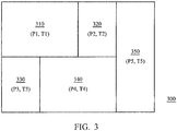
- FIG. 3 shows an example illustration of the layout 300 of an IC.
- the layout 300 is divided into a plurality of blocks 310-350 (step S220).
- each operation power (voltage and current) and each operation temperature are obtained for each of the blocks 310-350.
- block 310 has a first operation power P1 and a first operation temperature T1
- block 320 has a second operation power P2 and a second operation temperature T2
- block 330 has a third operation power P3 and a third operation temperature T3
- block 340 has a fourth operation power P4 and a fourth operation temperature T4
- block 350 has a fifth operation power P5 and a fifth operation temperature T5.
- the operation powers P1-P5 and the operation temperatures T1-T5 of the blocks 310-350 are the maximum operation powers and the maximum operation temperatures for each block.
- the maximum operation power and the maximum operation temperature are determined according to the number of gates in the block and the operation frequencies of the gates. Due to the number of gates and the operation frequencies of the gates being different from that of the other blocks, the operation powers and the operation temperatures of the blocks 310-350 may also be different.
- each wire of the block can be optimized, such as the width of each power wire having the smallest value, thereby each block of the layout can be minimized in terms of layout area.
- the widths of the power wires of each block will be limited by the maximum operation power of the whole blocks and the maximum operation temperature of the whole blocks.
- the method that uses the corresponding operation power and the corresponding operation temperature of the block to verify each block can minimize the size of the layout and decrease design manpower and cost.
- the width of each wire of each block can be optimized, especially the power wires in the block.
- FIG. 4 shows a computer system 400 according to an embodiment of the invention.
- the computer system 400 comprises a computer 410, a display device 420 and a user input interface 430, wherein the computer 410 comprises a processor 440, a memory 450, and a storage device 460.
- the computer 410 is coupled to the display device 420 and the user input interface 430, wherein the computer 410 is capable of operating an electronic design automation (EDA) tool.
- EDA electronic design automation
- the computer 410 is capable of receiving input instructions or information (e.g. circuit function information and power-related information) from the user input interface 430 and displaying the layout of the IC and the blocks of the layout on the display device 420.
- the display device 420 is a GUI for the computer 410.
- the display device 420 and the user input interface 430 can be implemented in the computer 410.
- the user input interface 430 may be a keyboard, a mouse, and so on.
- the storage device 460 can store the operating systems (OSs), applications, information (e.g. circuit function information and power-related information) and data that comprise input required by the applications and/or output generated by applications.
- the processor 440 of the computer 410 can perform one or more operations (either automatically or with user input) in any method that is implicitly or explicitly described in this disclosure.
- the processor 440 can load the applications of the storage device 460 into the memory 450, and then the applications can be used by the user to create, view, and/or edit a placement, a floor plan and a physical layout for a circuit design.
- a computer-readable storage medium may be, but is not limited to, volatile memory, non-volatile memory, magnetic and optical storage devices such as disk drives, magnetic tape, CDs (compact discs), DVDs (digital versatile discs or digital video discs), or other media, now known or later developed, that are capable of storing code and/or data.
- Examples of hardware modules or apparatuses described in this disclosure include, but are not limited to, application-specific integrated circuits (ASICs), field-programmable gate arrays (FPGAs), dedicated or shared processors, and/or other hardware modules or apparatuses now known or later developed.
- the methods and processes described in this disclosure can be partially or fully embodied as code and/or data stored in a computer-readable storage medium or device, so that when a computer system reads and executes the code and/or data, the computer system performs the associated methods and processes.
- the methods and processes can also be partially or fully embodied in hardware modules or apparatuses, so that when the hardware modules or apparatuses are activated, they perform the associated methods and processes. Note that the methods and processes can be embodied using a combination of code, data, and hardware modules or apparatuses.
Abstract
Description
- This application claims the benefit of
U.S. Provisional Application No. 62/326,896, filed on April 25, 2016 - The invention relates to a method for analyzing IR drop and electromigration (EM) of an integrated circuit (IC), and more particularly to a method for analyzing IR drop and electromigration (EM) of each block of an IC.
- In recent years, the development process for integrated circuits (ICs) such as super larger scale integrated circuits (LSIs) has generally employed computer assisted design (CAD). According to this CAD-based development process, abstract circuit data, which corresponds to the functions of an integrated circuit to be developed, is defined by using so-called hardware description language (HDL), and the defined circuit is used to form a concrete circuit structure to be mounted on a chip.
- Before the IC chips are manufactured (or implemented), the placements, the floor plans, and the layout areas of the IC chips are first considered so as to determine a die size for each IC chip. In general, the die size will affect the manufacturing cost of the IC chip. Therefore, it is desirable to minimize the layout area of the IC chip.
- Methods for analyzing IR drop and electromigration (EM) of an integrated circuit (IC) and a non-transitory computer-readable storage medium storing instructions are provided. An embodiment of a method for analyzing IR drop and EM of an IC is provided. The layout of an IC is obtained, wherein the layout is divided into a plurality of blocks, and each of the blocks corresponds to a specific function. Power-related information of the blocks is obtained. A specific operation power and a specific operation temperature are obtained according to the power-related information of each of the blocks. Each of the blocks is verified according to the corresponding specific operation power and the corresponding specific operation temperature.
- Furthermore, another embodiment of a method for analyzing IR drop and electromigration (EM) of an integrated circuit (IC) is provided. The layout of an IC is obtained, wherein the layout is divided into a plurality of blocks and each of the blocks corresponds to a specific function. A plurality of operation powers and a plurality of operation temperatures are obtained according to power-related information of the blocks, wherein each of the blocks has an individual operation power and an individual operation temperature. Each of the blocks is verified with the individual operation power and the individual operation temperature. The layout is adjusted when an IR drop violation or an EM violation is present in one of the verified blocks.
- Moreover, an embodiment is provided of a non-transitory computer-readable storage medium storing instructions that, when executed by a computer, cause the computer to perform a method for analyzing IR drop and electromigration (EM) of an integrated circuit (IC). The layout of an IC is obtained, wherein the layout is divided into a plurality of blocks and each of the blocks corresponds to a specific function. Power-related information of the blocks is obtained. A specific operation power and a specific operation temperature are obtained according to the power-related information of each of the blocks. The blocks are simultaneously verified according to the corresponding operation powers and the corresponding operation temperatures.
- A detailed description is given in the following embodiments with reference to the accompanying drawings.
- The invention can be more fully understood by reading the subsequent detailed description and examples with references made to the accompanying drawings, wherein:
-
FIG. 1 shows a flow chart illustrating a typical hierarchical design process of an integrated circuit (IC); -
FIG. 2 shows a method for analyzing IR drop and electromigration (EM) of an integrated circuit (IC) according to an embodiment of the invention, wherein the method ofFIG. 2 is performed by a computer capable of operating an electronic design automation (EDA) tool; -
FIG. 3 shows an example illustration of the layout of an IC; and -
FIG. 4 shows a computer system according to an embodiment of the invention. - The following description is of the best-contemplated mode of carrying out the invention. This description is made for the purpose of illustrating the general principles of the invention and should not be taken in a limiting sense. The scope of the invention is best determined by reference to the appended claims.
-
FIG. 1 shows a flow chart illustrating a typical hierarchical design process of an integrated circuit (IC). First, in step S110, a register-transfer level (RTL) code describing the function performed by the IC is obtained. Next, in step S120, the RTL code is synthesized to generate gates for the IC. In general, the IC comprises a plurality of blocks, and each block provides a significant function for the IC, such as a specific processor (e.g. an application processor, a video processor, an audio processor, or a controller), a memory (e.g. a SRAM module) and so on. Furthermore, each block has a corresponding RTL code, and then the RTL code of each block is synthesized to generate the gates of the block. Next, in step S130, a placement and routing procedure is performed to generate a layout of whole blocks within a chip area of the IC. For example, assuming that the IC comprises N blocks, N placements of the N blocks will have been generated according to the RTL codes of the blocks, respectively. Thus, according to the N placements of the N blocks and the gates that do not belong to the N blocks, a chip placement and routing procedure is performed and a layout is obtained. In some embodiments, the layout is a whole chip layout. In some embodiments, the layout is a portion of a whole chip layout regarding some digital circuits of the IC. Next, an analysis procedure is performed and the layout is verified to check whether the layout violates any of the various constraints or rules (step S140). If there are no violations in the layout, the IC is fabricated (or implemented) according to the layout (step S150). If a violation is present in the layout, the layout of the IC must be modified to handle the violation until no violations are present. - In the analysis procedure, structural data such as parasitic resistance and capacitance values is obtained according to the layout. Furthermore, a post-layout simulation is performed to ensure proper functionality. Post-layout simulation is used to predict the IC's true performance, by rigorously testing the actual loading of the circuits and power-bus lines. According to the results obtained in the post-layout simulation, some problems can be uncovered such as excessive power-bus voltage drop (e.g. IR drop) and electromigration (EM), which are generally not discoverable during RTL simulation.
- In general, EM refers to the dislodging of ions from a metal wire of the IC. When electrons flowing through a wire randomly collide into the atoms of the wire, the atoms are carried along the path of the electrons, thus causing wire deterioration. Furthermore, EM causes a gradual thinning out of the wire, and EM may lead to voltage drop across a wire, and eventually to a break in the wire. Specifically, EM is caused by current density (current flow divided by the width of the metal) exceeding a threshold value. For example, EM is generally most pronounced in thin wires with a relatively large amount of current flow (high current density). EM impedes the ability of metal to conduct, thereby reducing lifespan. Accordingly, if current density of a metal wire exceeds a specific threshold value, an EM violation is present in the metal wire of the layout of the IC. If the EM violation cannot be ignored, a correction is performed to address the EM violation.
- IR (or voltage) drop generally refers to a difference in voltage from a supply voltage (e.g. Vdd) at a power node and is usually caused by the resistance (either due to parasitic resistance or due to other devices in the metal wire) present between a voltage source (providing the supply voltage) and the power node. Therefore, devices connected to nodes other than the power node may receive a terminal voltage, which is less than the supply voltage. If the terminal voltage is less than a permissible threshold voltage, the devices may not operate in a normal mode. For example, a circuit may become non-operational or operate at a lower frequency (compared to an optimal frequency). Accordingly, if the voltage drop exceeds a specific threshold voltage, an IR drop violation is present in the metal wire of the layout of the IC. Similarly, if the IR drop violation cannot be ignored, a correction is performed to address the IR drop violation. Furthermore, IR drop at each node of the layout and current flow on each path may be determined by performing a simulation. The determined values may be used to ensure that the design is in conformity with various EM and IR drop requirements.
- In the analysis procedure, after no EM or IR drop violation that cannot be ignored is present, a design rule check (DRC) is performed on the layout to determine if there is a violation of the design rules associated with a given process. After the DRC successes, a layout-versus-schematic (LVS) is performed, so as to determine whether the layout corresponds to the original schematic, circuit diagram or RTL code of the IC design. As described above, after the layout is verified completely, a plurality of ICs are fabricated according to the layout.
-
FIG. 2 shows a method for analyzing IR drop and electromigration (EM) of an integrated circuit (IC) according to an embodiment of the invention, wherein the method ofFIG. 2 is performed by a computer capable of operating an electronic design automation (EDA) tool. First, in step S210, a processor of the computer obtains a layout of the IC, and the layout can be displayed in a graphical user interface (GUI). Next, in step S220, the processor divides the layout into a plurality of blocks according to circuit function information of the IC, and each block corresponds to a significant function for the IC, such as a specific processor (e.g. an application processor, a video processor, an audio processor, or a controller), a memory (e.g. a SRAM module) and so on. Next, in step S230, the processor obtains information regarding a plurality of operation powers (voltages and currents) of the blocks and a plurality of operation temperatures of the blocks according to power-related information of the blocks, wherein each block has an individual operation power (voltage and current) and an individual operation temperature. In some embodiments, the individual operation power and the individual operation temperature are the maximum operation power and the maximum operation temperature for the block. In some embodiments, the individual operation power and the individual operation temperature are determined according to the power consumption of the block. Next, the processor verifies each block with the individual operation power and the individual operation temperature corresponding to the verified block (step S240), so as to check whether an IR drop violation or an EM violation exists in the verified block (step S250). In some embodiments, the blocks are verified simultaneously. In some embodiments, the blocks are verified in a specific order. If the IR drop violation or the EM violation exists in the verified block and the violation cannot be ignored, the processor modifies the block to repair the violation (step S270), and then the layout of the IC is changed. In some embodiments, the processor modifies the block in the layout, so as to increase the widths of the wires corresponding to the violation in the block. In some embodiments, the processor may increase the area of the layout or change the shape of the layout, so as to repair the violation. After the block has been modified and the area or shape of the layout has not been changed (S280), the modified block is verified again (step S240). If the area or shape of the layout is changed, the method is performed again from step S210. Conversely, if no IR drop violation or EM violation exists in the verified block or the violation can be ignored, the layout is signed off (step S260) to perform subsequent procedures, such as DRC or LVS. -
FIG. 3 shows an example illustration of thelayout 300 of an IC. After obtaining circuit function information of the IC, thelayout 300 is divided into a plurality of blocks 310-350 (step S220). After obtaining power-related information of the blocks 310-350 of theIC 300, each operation power (voltage and current) and each operation temperature are obtained for each of the blocks 310-350. For example, block 310 has a first operation power P1 and a first operation temperature T1, block 320 has a second operation power P2 and a second operation temperature T2, block 330 has a third operation power P3 and a third operation temperature T3, block 340 has a fourth operation power P4 and a fourth operation temperature T4, and block 350 has a fifth operation power P5 and a fifth operation temperature T5. In some embodiments, the operation powers P1-P5 and the operation temperatures T1-T5 of the blocks 310-350 are the maximum operation powers and the maximum operation temperatures for each block. In general, the maximum operation power and the maximum operation temperature are determined according to the number of gates in the block and the operation frequencies of the gates. Due to the number of gates and the operation frequencies of the gates being different from that of the other blocks, the operation powers and the operation temperatures of the blocks 310-350 may also be different. By verifying each block with the corresponding power and the corresponding temperature, each wire of the block can be optimized, such as the width of each power wire having the smallest value, thereby each block of the layout can be minimized in terms of layout area. - For a conventional analysis procedure that uses a maximum operation power of the whole blocks and a maximum operation temperature of the whole blocks to verify whole blocks in a layout, the widths of the power wires of each block will be limited by the maximum operation power of the whole blocks and the maximum operation temperature of the whole blocks. Compared to the conventional analysis procedure, the method that uses the corresponding operation power and the corresponding operation temperature of the block to verify each block can minimize the size of the layout and decrease design manpower and cost. For example, the width of each wire of each block can be optimized, especially the power wires in the block.
-
FIG. 4 shows acomputer system 400 according to an embodiment of the invention. Thecomputer system 400 comprises acomputer 410, adisplay device 420 and auser input interface 430, wherein thecomputer 410 comprises aprocessor 440, amemory 450, and astorage device 460. Thecomputer 410 is coupled to thedisplay device 420 and theuser input interface 430, wherein thecomputer 410 is capable of operating an electronic design automation (EDA) tool. Furthermore, thecomputer 410 is capable of receiving input instructions or information (e.g. circuit function information and power-related information) from theuser input interface 430 and displaying the layout of the IC and the blocks of the layout on thedisplay device 420. In one embodiment, thedisplay device 420 is a GUI for thecomputer 410. Furthermore, thedisplay device 420 and theuser input interface 430 can be implemented in thecomputer 410. Theuser input interface 430 may be a keyboard, a mouse, and so on. In thecomputer 410, thestorage device 460 can store the operating systems (OSs), applications, information (e.g. circuit function information and power-related information) and data that comprise input required by the applications and/or output generated by applications. Theprocessor 440 of thecomputer 410 can perform one or more operations (either automatically or with user input) in any method that is implicitly or explicitly described in this disclosure. For example, during an operation, theprocessor 440 can load the applications of thestorage device 460 into thememory 450, and then the applications can be used by the user to create, view, and/or edit a placement, a floor plan and a physical layout for a circuit design. - The data structures and code described in this disclosure can be partially or fully stored on a computer-readable storage medium and/or a hardware module and/or hardware apparatus. A computer-readable storage medium may be, but is not limited to, volatile memory, non-volatile memory, magnetic and optical storage devices such as disk drives, magnetic tape, CDs (compact discs), DVDs (digital versatile discs or digital video discs), or other media, now known or later developed, that are capable of storing code and/or data. Examples of hardware modules or apparatuses described in this disclosure include, but are not limited to, application-specific integrated circuits (ASICs), field-programmable gate arrays (FPGAs), dedicated or shared processors, and/or other hardware modules or apparatuses now known or later developed.
- The methods and processes described in this disclosure can be partially or fully embodied as code and/or data stored in a computer-readable storage medium or device, so that when a computer system reads and executes the code and/or data, the computer system performs the associated methods and processes. The methods and processes can also be partially or fully embodied in hardware modules or apparatuses, so that when the hardware modules or apparatuses are activated, they perform the associated methods and processes. Note that the methods and processes can be embodied using a combination of code, data, and hardware modules or apparatuses.
- While the invention has been described by way of example and in terms of the preferred embodiments, it should be understood that the invention is not limited to the disclosed embodiments. On the contrary, it is intended to cover various modifications and similar arrangements (as would be apparent to those skilled in the art). Therefore, the scope of the appended claims should be accorded the broadest interpretation so as to encompass all such modifications and similar arrangements.
Claims (10)
- A method for analyzing IR drop and electromigration (EM) of an integrated circuit (IC), comprising:obtaining a layout of an IC, wherein the layout is divided into a plurality of blocks and each of the blocks corresponds to a specific function;obtaining power-related information of the blocks;obtaining a specific operation power and a specific operation temperature according to the power-related information of each of the blocks; andverifying each of the blocks according to the corresponding specific operation power and the corresponding specific operation temperature.
- The method as claimed in claim 1, further comprising:checking whether an IR drop violation or an EM violation is present when each of the blocks is verified.
- The method of claim 2, further comprising:adjusting the layout when the IR drop violation or the EM violation is present in the verified block.
- The method as claimed in claim 3, wherein the step of adjusting the layout when the IR drop violation or the EM violation is present in the verified block further comprises:increasing width of at least one wire of the verified block corresponding to the IR drop violation or the EM violation.
- The method as claimed in claim 4, further comprising:re-verifying the block with the increased width of the at least one wire according to the corresponding operation power and the corresponding operation temperature.
- The method as claimed in one of the preceding claims, further comprising:fabricating the IC according to the layout when no IR drop violation or no EM violation is present in each of the blocks.
- The method as claimed in one of the preceding claims, wherein the specific operation power and the specific operation temperature are determined according to a power consumption of the corresponding block.
- The method as claimed in one of the preceding claims, wherein the specific operation power and the specific operation temperature of the block are different from that of the other blocks.
- The method as claimed in one of the preceding claims, wherein the specific functions of the blocks are different.
- A non-transitory computer-readable storage medium storing instructions that, when executed by a computer, cause the computer to perform the method of one of the preceding claims.
Applications Claiming Priority (2)
| Application Number | Priority Date | Filing Date | Title |
|---|---|---|---|
| US201662326896P | 2016-04-25 | 2016-04-25 | |
| US15/438,844 US20170308639A1 (en) | 2016-04-25 | 2017-02-22 | Method for analyzing ir drop and electromigration of ic |
Publications (1)
| Publication Number | Publication Date |
|---|---|
| EP3239865A1 true EP3239865A1 (en) | 2017-11-01 |
Family
ID=58227985
Family Applications (1)
| Application Number | Title | Priority Date | Filing Date |
|---|---|---|---|
| EP17159087.0A Withdrawn EP3239865A1 (en) | 2016-04-25 | 2017-03-03 | Method for analyzing ir drop and electromigration of ic |
Country Status (4)
| Country | Link |
|---|---|
| US (1) | US20170308639A1 (en) |
| EP (1) | EP3239865A1 (en) |
| CN (1) | CN107403024A (en) |
| TW (1) | TWI640883B (en) |
Families Citing this family (5)
| Publication number | Priority date | Publication date | Assignee | Title |
|---|---|---|---|---|
| US10810346B2 (en) * | 2018-09-28 | 2020-10-20 | Taiwan Semiconductor Manufacturing Co., Ltd. | Static voltage drop (SIR) violation prediction systems and methods |
| CN112749526A (en) * | 2019-10-30 | 2021-05-04 | 瑞昱半导体股份有限公司 | Power rail design method, apparatus and non-transitory computer readable medium thereof |
| CN112115676B (en) * | 2020-09-29 | 2021-10-26 | 飞腾信息技术有限公司 | Static voltage drop repairing method, device, equipment and storage medium |
| CN112289697A (en) * | 2020-10-20 | 2021-01-29 | 上海兆芯集成电路有限公司 | Verification method |
| TWI769829B (en) | 2021-05-21 | 2022-07-01 | 崛智科技有限公司 | Device and method for integrated circuit assistance design, and method for constructing electrical performance gradient model |
Citations (5)
| Publication number | Priority date | Publication date | Assignee | Title |
|---|---|---|---|---|
| US20060026540A1 (en) * | 2004-07-29 | 2006-02-02 | Texas Instruments Incorporated | Electro-migration (EM) and Voltage (IR) Drop Analysis of Integrated Circuit (IC) Designs |
| US20080098340A1 (en) * | 2004-12-06 | 2008-04-24 | Entasys Design, Inc. | Method for Designing Block Placement and Power Distribution of Semiconductor Integrated Circuit |
| US20090024969A1 (en) * | 2004-01-28 | 2009-01-22 | Rajit Chandra | Semiconductor chip design having thermal awareness across multiple sub-system domains |
| US20090031264A1 (en) * | 2007-07-24 | 2009-01-29 | Dan Rittman | System and method for finding electromigration, self heat and voltage drop violations of an integrated circuit when its design and electrical characterization are incomplete |
| US9208277B1 (en) * | 2011-08-19 | 2015-12-08 | Cadence Design Systems, Inc. | Automated adjustment of wire connections in computer-assisted design of circuits |
Family Cites Families (17)
| Publication number | Priority date | Publication date | Assignee | Title |
|---|---|---|---|---|
| US5349542A (en) * | 1992-04-02 | 1994-09-20 | Vlsi Technology, Inc. | Method for sizing widths of power busses in integrated circuits |
| TWI266215B (en) * | 2002-08-12 | 2006-11-11 | Silicon Integrated Sys Corp | Method for analyzing power noise and method for reducing the same |
| JP4287294B2 (en) * | 2004-01-21 | 2009-07-01 | 株式会社東芝 | Automatic design method, automatic design apparatus, and semiconductor integrated circuit |
| US20090224356A1 (en) * | 2004-01-28 | 2009-09-10 | Rajit Chandra | Method and apparatus for thermally aware design improvement |
| JP2006164132A (en) * | 2004-12-10 | 2006-06-22 | Matsushita Electric Ind Co Ltd | Method for net list creation and method for layout design for semiconductor integrated circuit |
| US7266797B2 (en) * | 2005-05-19 | 2007-09-04 | International Business Machines Corporation | Automated and electrically robust method for placing power gating switches in voltage islands |
| US8667455B1 (en) * | 2010-06-11 | 2014-03-04 | Worldwide Pro Ltd. | Hierarchical visualization-based analysis of integrated circuits |
| US8689169B2 (en) * | 2010-07-24 | 2014-04-01 | Cadence Design Systems, Inc. | Method, apparatus, and article of manufacture for providing in situ, customizable information in designing electronic circuits with electrical awareness |
| US8769475B2 (en) * | 2011-10-31 | 2014-07-01 | Taiwan Semiconductor Manufacturing Co., Ltd. | Method, system and software for accessing design rules and library of design features while designing semiconductor device layout |
| US8826203B2 (en) * | 2012-06-18 | 2014-09-02 | International Business Machines Corporation | Automating current-aware integrated circuit and package design and optimization |
| US9541603B2 (en) * | 2013-07-10 | 2017-01-10 | Apple Inc. | Method and apparatus for power glitch detection in integrated circuits |
| US9213797B2 (en) * | 2013-11-15 | 2015-12-15 | Taiwan Semiconductor Manufacturing Company, Ltd. | Method, system and computer program product for designing semiconductor device |
| US9665680B2 (en) * | 2014-05-30 | 2017-05-30 | Regents Of The University Of Minnesota | Cell-level signal electromigration |
| US20150356229A1 (en) * | 2014-06-09 | 2015-12-10 | Qualcomm Incorporated | Physical cell electromigration data generation |
| CN104601019B (en) * | 2014-12-19 | 2017-07-04 | 广东美的制冷设备有限公司 | SPM, power device and its temperature sensing circuit and method |
| US9767240B2 (en) * | 2015-11-19 | 2017-09-19 | Globalfoundries Inc. | Temperature-aware integrated circuit design methods and systems |
| US9791880B2 (en) * | 2016-03-16 | 2017-10-17 | Analog Devices Global | Reducing voltage regulator transistor operating temperatures |
-
2017
- 2017-02-22 US US15/438,844 patent/US20170308639A1/en not_active Abandoned
- 2017-03-03 EP EP17159087.0A patent/EP3239865A1/en not_active Withdrawn
- 2017-04-19 TW TW106113056A patent/TWI640883B/en not_active IP Right Cessation
- 2017-04-20 CN CN201710259376.8A patent/CN107403024A/en not_active Withdrawn
Patent Citations (5)
| Publication number | Priority date | Publication date | Assignee | Title |
|---|---|---|---|---|
| US20090024969A1 (en) * | 2004-01-28 | 2009-01-22 | Rajit Chandra | Semiconductor chip design having thermal awareness across multiple sub-system domains |
| US20060026540A1 (en) * | 2004-07-29 | 2006-02-02 | Texas Instruments Incorporated | Electro-migration (EM) and Voltage (IR) Drop Analysis of Integrated Circuit (IC) Designs |
| US20080098340A1 (en) * | 2004-12-06 | 2008-04-24 | Entasys Design, Inc. | Method for Designing Block Placement and Power Distribution of Semiconductor Integrated Circuit |
| US20090031264A1 (en) * | 2007-07-24 | 2009-01-29 | Dan Rittman | System and method for finding electromigration, self heat and voltage drop violations of an integrated circuit when its design and electrical characterization are incomplete |
| US9208277B1 (en) * | 2011-08-19 | 2015-12-08 | Cadence Design Systems, Inc. | Automated adjustment of wire connections in computer-assisted design of circuits |
Also Published As
| Publication number | Publication date |
|---|---|
| CN107403024A (en) | 2017-11-28 |
| TWI640883B (en) | 2018-11-11 |
| US20170308639A1 (en) | 2017-10-26 |
| TW201738789A (en) | 2017-11-01 |
Similar Documents
| Publication | Publication Date | Title |
|---|---|---|
| EP3239865A1 (en) | Method for analyzing ir drop and electromigration of ic | |
| US20080127020A1 (en) | System and method for automatic elimination of voltage drop, also known as IR drop, violations of a mask layout block, maintaining the process design rules correctness | |
| US9367660B2 (en) | Electromigration-aware layout generation | |
| US9767240B2 (en) | Temperature-aware integrated circuit design methods and systems | |
| US9740815B2 (en) | Electromigration-aware integrated circuit design methods and systems | |
| US9189591B2 (en) | Path-based floorplan analysis | |
| US11030383B2 (en) | Integrated device and method of forming the same | |
| US9147030B2 (en) | Multiple-instantiated-module (mim) aware pin assignment | |
| EP2529283A2 (en) | Zone-based leakage power optimization | |
| US8151229B1 (en) | System and method of computing pin criticalities under process variations for timing analysis and optimization | |
| US10223485B2 (en) | Reliability verification based on combining voltage propagation with simulation | |
| US10891411B2 (en) | Hierarchy-driven logical and physical synthesis co-optimization | |
| US9940422B2 (en) | Methods for reducing congestion region in layout area of IC | |
| US11574101B2 (en) | Techniques for providing optimizations based on categories of slack in timing paths | |
| US10162927B2 (en) | Methods for redistributing cell densities in layout area of IC | |
| US8418116B2 (en) | Zone-based optimization framework for performing timing and design rule optimization | |
| US10922470B2 (en) | Method and system of forming semiconductor device | |
| US7546562B1 (en) | Physical integrated circuit design with uncertain design conditions | |
| WO2009002301A1 (en) | System and method for automatic elimination of voltage drop | |
| CN112749526A (en) | Power rail design method, apparatus and non-transitory computer readable medium thereof | |
| US10049174B2 (en) | Exact delay synthesis | |
| JP4855283B2 (en) | Semiconductor integrated circuit design equipment | |
| US9189583B2 (en) | Look-up based buffer tree synthesis | |
| EP4152201A1 (en) | Systems and methods for circuit design dependent programmable maximum junction temperatures | |
| US20140351778A1 (en) | Lsi design apparatus and method of designing lsi |
Legal Events
| Date | Code | Title | Description |
|---|---|---|---|
| PUAI | Public reference made under article 153(3) epc to a published international application that has entered the european phase |
Free format text: ORIGINAL CODE: 0009012 |
|
| AK | Designated contracting states |
Kind code of ref document: A1 Designated state(s): AL AT BE BG CH CY CZ DE DK EE ES FI FR GB GR HR HU IE IS IT LI LT LU LV MC MK MT NL NO PL PT RO RS SE SI SK SM TR |
|
| AX | Request for extension of the european patent |
Extension state: BA ME |
|
| 17P | Request for examination filed |
Effective date: 20180427 |
|
| RBV | Designated contracting states (corrected) |
Designated state(s): AL AT BE BG CH CY CZ DE DK EE ES FI FR GB GR HR HU IE IS IT LI LT LU LV MC MK MT NL NO PL PT RO RS SE SI SK SM TR |
|
| 17Q | First examination report despatched |
Effective date: 20180913 |
|
| STAA | Information on the status of an ep patent application or granted ep patent |
Free format text: STATUS: THE APPLICATION HAS BEEN WITHDRAWN |
|
| 18W | Application withdrawn |
Effective date: 20181016 |