EP3236285A1 - Optoelektronischer sensor - Google Patents
Optoelektronischer sensor Download PDFInfo
- Publication number
- EP3236285A1 EP3236285A1 EP17162805.0A EP17162805A EP3236285A1 EP 3236285 A1 EP3236285 A1 EP 3236285A1 EP 17162805 A EP17162805 A EP 17162805A EP 3236285 A1 EP3236285 A1 EP 3236285A1
- Authority
- EP
- European Patent Office
- Prior art keywords
- mirror
- optoelectronic sensor
- sensor according
- mirror element
- light
- Prior art date
- Legal status (The legal status is an assumption and is not a legal conclusion. Google has not performed a legal analysis and makes no representation as to the accuracy of the status listed.)
- Granted
Links
Images


Classifications
-
- G—PHYSICS
- G02—OPTICS
- G02B—OPTICAL ELEMENTS, SYSTEMS OR APPARATUS
- G02B5/00—Optical elements other than lenses
- G02B5/08—Mirrors
- G02B5/0808—Mirrors having a single reflecting layer
-
- B—PERFORMING OPERATIONS; TRANSPORTING
- B29—WORKING OF PLASTICS; WORKING OF SUBSTANCES IN A PLASTIC STATE IN GENERAL
- B29D—PRODUCING PARTICULAR ARTICLES FROM PLASTICS OR FROM SUBSTANCES IN A PLASTIC STATE
- B29D11/00—Producing optical elements, e.g. lenses or prisms
- B29D11/00009—Production of simple or compound lenses
- B29D11/0048—Moulds for lenses
- B29D11/00576—Moulds for lenses with means to engage flash, e.g. HEMA ring
- B29D11/00586—Moulds for lenses with means to engage flash, e.g. HEMA ring and removing the flash or HEMA ring
-
- G—PHYSICS
- G01—MEASURING; TESTING
- G01S—RADIO DIRECTION-FINDING; RADIO NAVIGATION; DETERMINING DISTANCE OR VELOCITY BY USE OF RADIO WAVES; LOCATING OR PRESENCE-DETECTING BY USE OF THE REFLECTION OR RERADIATION OF RADIO WAVES; ANALOGOUS ARRANGEMENTS USING OTHER WAVES
- G01S17/00—Systems using the reflection or reradiation of electromagnetic waves other than radio waves, e.g. lidar systems
- G01S17/02—Systems using the reflection of electromagnetic waves other than radio waves
- G01S17/04—Systems determining the presence of a target
-
- G—PHYSICS
- G01—MEASURING; TESTING
- G01S—RADIO DIRECTION-FINDING; RADIO NAVIGATION; DETERMINING DISTANCE OR VELOCITY BY USE OF RADIO WAVES; LOCATING OR PRESENCE-DETECTING BY USE OF THE REFLECTION OR RERADIATION OF RADIO WAVES; ANALOGOUS ARRANGEMENTS USING OTHER WAVES
- G01S17/00—Systems using the reflection or reradiation of electromagnetic waves other than radio waves, e.g. lidar systems
- G01S17/02—Systems using the reflection of electromagnetic waves other than radio waves
- G01S17/06—Systems determining position data of a target
- G01S17/08—Systems determining position data of a target for measuring distance only
-
- G—PHYSICS
- G01—MEASURING; TESTING
- G01S—RADIO DIRECTION-FINDING; RADIO NAVIGATION; DETERMINING DISTANCE OR VELOCITY BY USE OF RADIO WAVES; LOCATING OR PRESENCE-DETECTING BY USE OF THE REFLECTION OR RERADIATION OF RADIO WAVES; ANALOGOUS ARRANGEMENTS USING OTHER WAVES
- G01S17/00—Systems using the reflection or reradiation of electromagnetic waves other than radio waves, e.g. lidar systems
- G01S17/02—Systems using the reflection of electromagnetic waves other than radio waves
- G01S17/06—Systems determining position data of a target
- G01S17/46—Indirect determination of position data
- G01S17/48—Active triangulation systems, i.e. using the transmission and reflection of electromagnetic waves other than radio waves
-
- G—PHYSICS
- G01—MEASURING; TESTING
- G01S—RADIO DIRECTION-FINDING; RADIO NAVIGATION; DETERMINING DISTANCE OR VELOCITY BY USE OF RADIO WAVES; LOCATING OR PRESENCE-DETECTING BY USE OF THE REFLECTION OR RERADIATION OF RADIO WAVES; ANALOGOUS ARRANGEMENTS USING OTHER WAVES
- G01S7/00—Details of systems according to groups G01S13/00, G01S15/00, G01S17/00
- G01S7/48—Details of systems according to groups G01S13/00, G01S15/00, G01S17/00 of systems according to group G01S17/00
- G01S7/481—Constructional features, e.g. arrangements of optical elements
- G01S7/4811—Constructional features, e.g. arrangements of optical elements common to transmitter and receiver
- G01S7/4812—Constructional features, e.g. arrangements of optical elements common to transmitter and receiver transmitted and received beams following a coaxial path
-
- G—PHYSICS
- G01—MEASURING; TESTING
- G01V—GEOPHYSICS; GRAVITATIONAL MEASUREMENTS; DETECTING MASSES OR OBJECTS; TAGS
- G01V8/00—Prospecting or detecting by optical means
- G01V8/10—Detecting, e.g. by using light barriers
- G01V8/12—Detecting, e.g. by using light barriers using one transmitter and one receiver
- G01V8/14—Detecting, e.g. by using light barriers using one transmitter and one receiver using reflectors
-
- G—PHYSICS
- G01—MEASURING; TESTING
- G01S—RADIO DIRECTION-FINDING; RADIO NAVIGATION; DETERMINING DISTANCE OR VELOCITY BY USE OF RADIO WAVES; LOCATING OR PRESENCE-DETECTING BY USE OF THE REFLECTION OR RERADIATION OF RADIO WAVES; ANALOGOUS ARRANGEMENTS USING OTHER WAVES
- G01S7/00—Details of systems according to groups G01S13/00, G01S15/00, G01S17/00
- G01S7/48—Details of systems according to groups G01S13/00, G01S15/00, G01S17/00 of systems according to group G01S17/00
- G01S7/481—Constructional features, e.g. arrangements of optical elements
- G01S7/4811—Constructional features, e.g. arrangements of optical elements common to transmitter and receiver
- G01S7/4813—Housing arrangements
Definitions
- the present invention relates to an optoelectronic sensor according to the preamble of claim 1.
- optical carriers made of polymer materials are used.
- optical carriers made of polymer materials
- the problem here are the tolerances and precision of the optics carrier.
- Another problem is a strength of the optical carrier, a temperature dependence, and complex processes to produce reflective surfaces on the plastic part.
- conductive shrouds are often required to ensure electromagnetic compatibility (EMC).
- An object of the invention is to provide a mirror element for an optoelectronic sensor, which is inexpensive and has a high surface quality.
- the mirror element should have low tolerances and have a low coefficient of thermal expansion.
- an optoelectronic sensor for detecting objects within a surveillance area, comprising a transmitter unit having a transmitting element for emitting transmitted light beams into the surveillance area, and / or a receiver unit having a receiving element for receiving receiving light beams of the object, wherein the Receiver unit and / or the transmitter unit has at least one mirror element for deflecting the light rays, wherein the mirror element is formed of amorphous metal.
- Amorphous metals or amorphous metal materials which are also referred to as metallic glasses, have due to their non-crystalline structure compared to steel on an electrical conductivity, which is less than in steel.
- the strength and hardness of amorphous metals are increased compared to crystalline metals. This increased strength makes it possible to form thinner surfaces with the same strength. As a result, the mirror element can be formed thin-walled.
- Another advantage of the invention is that amorphous metals have comparatively low shrinkage rates and can therefore be produced tool-bound by means of injection-molding-like processes. This allows a particularly fast and cost-effective production of the mirror element and thus of the optoelectronic sensor.
- the mirror element is made entirely by an injection molding process. Accordingly, the mirror element is designed as an injection-molded component. This allows a particularly simple and inexpensive production. In the case of crystalline metals, production by means of injection molding would be disadvantageous due to the high shrinkage rates.
- the mirror element has low tolerance values, whereby the mirror element can be manufactured with high precision.
- the surface quality of the mirror element can be made very high.
- a high surface quality of the mirror surface or of the mirror can already be produced or provided by the injection-molded component without subsequent processing since the surface quality of the molded part itself already has a high surface quality.
- the mirror element is also inexpensive to produce.
- the amorphous metal has a low temperature expansion coefficient.
- the optical properties of the mirror element change only slightly with temperature changes.
- an optoelectronic sensor is formed with constant optical properties in the event of a temperature change.
- the optoelectronic sensor is preferably a light barrier, a reflection light barrier or a light sensor.
- a light barrier can be designed as a through-beam sensor.
- the light transmitter and the light receiver are arranged opposite one another and an interruption of the light beam leads in the evaluation unit of the light receiver to an object detection signal.
- the light transmitter or transmitter unit and the light receiver or receiver unit are accommodated on the same side of a monitoring area, usually in a single housing.
- a retroreflector is arranged, which reflects the light emitted by the light emitter back through 180 ° in the light receiver.
- the light transmitter or transmitter unit and the light receiver or receiver unit are arranged in a common housing.
- the light rays emitted by the light emitter are reflected or remitted on an object.
- the received light can be evaluated energetically. If a certain threshold is exceeded, an object detection signal is output.
- the light sensor can also be designed as Triangulationstaster.
- a Triangulationstaster the receiving element is spatially resolved and arranged the light emitter spaced from the receiving element.
- a light spot emitted by the light emitter is returned by an object, imaged via the reception lens onto the spatially resolving reception element.
- the light spot is imaged at different positions, it being possible to infer the distance of the object from the position of the light spot on the receiving element.
- a sensor can also be a sensor according to the light transit time method.
- a short light pulse or a group of light pulses is emitted by the light transmitter.
- the one or more light pulses are reflected or remitted by an object and received by the receiving element of the light receiver. From a downstream evaluation unit, the duration of the light from sending to receiving evaluated and calculated from the distance of the object.
- the amorphous metal is an amorphous metal alloy.
- Such amorphous metal alloys are available in a variety of designs and are relatively inexpensive compared to alternative crystalline metals such as titanium.
- the type of alloy can be tailored to the particular application.
- a defined electrical potential is connected to the mirror element.
- the defined electrical potential of the sensor is an electrical potential which is connected to the electronic card of the sensor.
- the electrical potential is connected, for example, from the electronic board via a conductive or metallic contact or a metallic pin to the mirror element. By the conductive contact, an electrical connection between the mirror element and the electronic board is produced when mounting the mirror element. As a result, the electromagnetic compatibility of the optoelectronic sensor is improved.
- the mirror of the mirror element is concavely curved.
- the mirror is thus curved inwards, whereby a concave mirror is formed.
- light rays falling on the mirror can be focused or focused through the mirror.
- an additional optical component such. As a lens can be saved.
- the mirror of the mirror element is planar.
- a plane or flat mirror reflects the light at each point identically with parallel incident light rays.
- a plane mirror can also have a focusing effect if the incident light beams are already converging.
- the mirror element is arranged in a mirror carrier, wherein the mirror element and the mirror carrier are integrally formed and made of amorphous metal.
- the mirror support forms, for example, a frame for the mirror element, as a result of which the mirror element is made mechanically more stable. This ensures a particularly simple, robust and stable design.
- the mirror carrier has, for example, additional side walls.
- the mirror support serves as a mounting base for other sensor components.
- the mirror carrier has, for example, fastening receptacles for a sensor housing.
- the mirror support may have reference surfaces for positioning other sensor components.
- the mirror support may have reference surfaces in order to position the mirror support itself and thus the mirror element itself relative to another reference surface in order to ensure an exact alignment of the mirror element.
- the mirror support has a complex structure.
- This complex structure can be used for attachment and can be adapted to the shape of other adjacent components, so that the most compact possible sensor is formed.
- At least two mirror elements and the mirror carrier are integrally formed.
- received light beams can be deflected twice by the successively arranged mirror elements in order to supply them, for example, to a receiving element.
- the respective mirror elements can also be designed differently.
- a first mirror element may be concave and a second mirror element may be flat.
- a plurality of mirror elements are provided for a plurality of transmitting units or for a plurality of receiving units.
- At least one mirror element has an opening for the transmitted light beams.
- the transmitter unit can be integrated with the transmitter element in the mirror element for the receiver unit, resulting in a compact sensor.
- the transmitted light beams and the received light beams may be collimated.
- the opening is preferably a round opening or a hole, which is arranged, for example, near the middle or in the center in the mirror element.
- the mirror element or the mirror support is mechanically connected to a printed circuit board.
- a printed circuit board This allows the sensor to be very simple. For example, all electronic components are arranged on the circuit board and arranged on the mirror support all optical components. As a result, the sensor is almost completely built up by the mechanical connection of the mirror carrier with the printed circuit board. Only an optional electrical connection and the sensor housing need to be supplemented to obtain an operational optoelectronic sensor.
- the transmitting element and / or the receiving element and an evaluation unit is arranged on the printed circuit board.
- the printed circuit board optionally has at least one reference surface which is connected to at least one optional reference surface of the mirror carrier. By the transmitting element and / or the receiving element is aligned and referenced to the mirror element.
- the mirror support has at least one receptacle for at least one optical element.
- the optical element can, for example, be at least one refractive element, for example at least one lens, for example a lens, for example at least one diffractive element or, for example, at least one light-guiding element, for example at least one light guide.
- the mirror carrier in turn has reference surfaces for the optical element.
- the optical element is a converging lens.
- the mirror carrier in addition to the mirror element, has at least one surface which is formed integrally with the mirror carrier in order to form an EMC shielding surface.
- a plurality of surfaces may be provided which surround the electronics of the circuit board, so that the electronics of the circuit board is shielded, whereby the sensor has a better electromagnetic compatibility.
- the sensor is better protected against interfering foreign electromagnetic waves.
- the mirror element is automatically equipped on a printed circuit board.
- an entire sensor unit consisting of at least one populated printed circuit board and the mirror element can be produced automatically.
- the sensor is very inexpensive to produce.
- FIG. 1 shows an optoelectronic sensor 1 with a housing 21, a windscreen 22 and an electrical connection 23rd
- the optoelectronic sensor 1 is preferably a light barrier, a reflection light barrier, a light sensor, or a distance sensor.
- a reflection light barrier the light transmitter or transmitter unit and the light receiver or receiver unit are accommodated on the same side of a monitoring area, usually in a single housing.
- a retroreflector is arranged, which reflects the light emitted by the light emitter back through 180 ° in the light receiver.
- the light transmitter or transmitter unit and the light receiver or receiver unit are arranged in a common housing.
- the light rays emitted by the light emitter are reflected or remitted on an object.
- FIG. 2 shows the internal structure of the optoelectronic sensor 1 without housing.
- FIG. 2 shows an optoelectronic sensor 1 for detecting objects 2 within a monitoring area 3, with a transmitter unit 4 with a transmitting element 5 for emitting transmitted light beams 6 in the surveillance area 3, and a receiver unit 7 with a receiving element 8 for receiving received light beams 9 of the object 2, wherein the receiver unit 7 has at least one mirror element 10 for deflecting the received light beams 9, wherein the mirror element 10 is formed from amorphous metal 11.
- the mirror element 10 is completely made by an injection molding process.
- a high surface quality of the mirror surface or of the mirror 12 can already be produced or provided by the injection-molded component without subsequent processing.
- the amorphous metal 11 is an amorphous metal alloy.
- a defined electrical potential is connected to the mirror element 10.
- the defined electrical potential of the optoelectronic sensor 1 is an electrical potential which is connected to the printed circuit board 15 or electronic card of the optoelectronic sensor 1.
- the electrical potential is connected, for example, from the printed circuit board 15 via a conductive or metallic contact or a metallic pin to the mirror element.
- the mirror 12 of the mirror element 10 is concavely curved.
- the mirror 12 is thus curved inwards, whereby a concave mirror is formed.
- receiving light beams 9 falling on the mirror 12 can be focused or focused by the mirror 12.
- FIG. 3 which is a sectional view according to FIG. 2 represents, is a second mirror 12.1 of the mirror element 10.1 formed plan.
- the mirror elements 10, 10.1 are arranged in a mirror support 13, wherein the mirror elements 10, 10.1 and the mirror support 13 are integrally formed and consist of amorphous metal 11.
- the mirror support 13 forms, for example, a frame for the mirror elements 10, 10.1, whereby the mirror elements 10, 10.1 are made mechanically more stable. This ensures a particularly simple, robust and stable design.
- the mirror carrier 13 has, for example, additional side walls 24.
- the mirror support 13 serves as a mounting base for other sensor components.
- a connection unit 25 can be attached to the mirror support 13.
- the mirror support 13 has, for example, fastening receptacles for a sensor housing.
- the mirror support 13 may have reference surfaces for positioning other sensor components.
- the mirror support 13 can have reference surfaces in order to precisely position the mirror support 13 and thus the mirror elements 10, 10.1 themselves relative to another reference surface in order to ensure exact alignment of the mirror elements 10, 10.1.
- the mirror carrier 13 has a complex structure or complex surface.
- This complex structure or complex surface can be used for attachment serve and can be adapted to the shape of other adjacent components, so that a compact optoelectronic sensor 1 is formed as possible.
- At least two mirror elements 10, 10.1 and the mirror support 13 are integrally formed.
- received light beams can be deflected twice by the successively arranged mirror elements 10, 10.1 in order, for example, to supply them to a receiving element.
- the respective mirror elements 10, 10.1 are formed differently.
- a first mirror element 10 is concave and a second mirror element 10.1 is planar.
- the mirror element 10 has an opening 14 for the transmitted light beams 6.
- the transmitter unit 4 with the transmitter element 5 can be integrated in the mirror element 10 for the receiver unit 7.
- the transmitted light beams 6 and the received light beams 9 can be collimated.
- the opening 14 is preferably a round opening 14 or a hole which is arranged, for example, near the middle or in the middle in the mirror element 10.
- the mirror element 10 or the mirror support 13 is mechanically connected to a printed circuit board 15.
- all electronic components are arranged on the printed circuit board 15 and all optical components are arranged on the mirror carrier 13.
- the optoelectronic sensor 1 is almost completely built up by the mechanical connection of the mirror carrier 13 with the circuit board 15. Only an optional electrical connection and the sensor housing must be supplemented to obtain an operational optoelectronic sensor 1.
- the transmitting element 5 and / or the receiving element 8 and an evaluation unit is arranged on the printed circuit board 15.
- the printed circuit board optionally has at least one reference surface, which is connected to at least one optional reference surface of the mirror carrier 13. As a result, the transmitting element 5 and the receiving element 8 are aligned and referenced to the mirror element 10.
- the mirror carrier 13 has at least one receptacle 16 for at least one optical element 17.
- the optical element 17 can be, for example, at least one refractive element, for example at least one converging lens 18.
- the mirror carrier 13 in turn has reference surfaces for the optical element 17.
- the mirror support 13 in addition to the mirror elements 10, 10.1 at least one surface 19 which is integrally formed to the mirror support 13 to form an EMC shielding surface 20.
- a plurality of surfaces 19 may be provided which shield the electronics of the circuit board 15, so that the electronics of the circuit board 15 is shielded, whereby the optoelectronic sensor 1 has a better electromagnetic compatibility.
- FIG. 2 is the mirror support 13 and the mirror elements 10, 10.1 automatically equipped on a printed circuit board 15.
Landscapes
- Physics & Mathematics (AREA)
- Engineering & Computer Science (AREA)
- Electromagnetism (AREA)
- General Physics & Mathematics (AREA)
- Remote Sensing (AREA)
- Computer Networks & Wireless Communication (AREA)
- Radar, Positioning & Navigation (AREA)
- Life Sciences & Earth Sciences (AREA)
- Optics & Photonics (AREA)
- General Life Sciences & Earth Sciences (AREA)
- Geophysics (AREA)
- Health & Medical Sciences (AREA)
- Manufacturing & Machinery (AREA)
- Ophthalmology & Optometry (AREA)
- Mechanical Engineering (AREA)
- Light Receiving Elements (AREA)
- Geophysics And Detection Of Objects (AREA)
Abstract
Description
- Die vorliegende Erfindung betrifft einen optoelektronischen Sensor nach dem Oberbegriff von Anspruch 1.
- Für den Einsatz in optoelektronischen Sensoren werden sogenannte Optikträger aus Polymerwerkstoffen eingesetzt. Durch bekannte Spritzgussverfahren lässt sich eine komplexe Optikträgergeometrie günstig herstellen. Problematisch dabei sind die Toleranzen und eine Präzision des Optikträgers. Weiter problematisch ist eine Festigkeit des Optikträgers, eine Temperaturabhängigkeit, sowie aufwändige Prozesse, um spiegelnde Oberflächen auf dem Kunststoffteil herzustellen. Zusätzlich sind häufig leitfähige Schirmbleche erforderlich, um eine elektromagnetische Verträglichkeit (EMV) sicherzustellen.
- Eine Aufgabe der Erfindung besteht darin, ein Spiegelelement für einen optoelektronischen Sensor bereitzustellen, welches kostengünstig ist und eine hohe Oberflächengüte aufweist. Weiter soll das Spiegelelement niedrige Toleranzen aufweisen und einen niedrigen Temperaturausdehnungskoeffizienten aufweisen.
- Die Aufgabe wird gemäß Anspruch 1 gelöst durch einen optoelektronischen Sensor zur Erkennung von Objekten innerhalb eines Überwachungsbereichs, mit einer Sendereinheit mit einem Sendeelement zur Aussendung von Sendelichtstrahlen in den Überwachungsbereich, und/oder einer Empfängereinheit mit einem Empfangselement zum Empfang von Empfangslichtstrahlen des Objektes, wobei die Empfängereinheit und/oder die Sendereinheit mindestens ein Spiegelelement aufweist zur Umlenkung der Lichtstrahlen, wobei das Spiegelelement aus amorphem Metall gebildet ist.
- Amorphe Metalle bzw. amorphe Metallwerkstoffe, welche auch als metallische Gläser bezeichnet werden, weisen aufgrund ihrer nicht kristallinen Struktur im Vergleich zu Stahl eine elektrische Leitfähigkeit auf, die jedoch geringer ist als bei Stahl. Zusätzlich sind die Festigkeit und die Härte von amorphen Metallen im Vergleich zu kristallinen Metallen erhöht. Diese erhöhte Festigkeit ermöglicht es, dünnere Flächen auszubilden bei gleicher Festigkeit. Dadurch kann das Spiegelelement dünnwandig ausgebildet werden.
- Ein weiterer Vorteil der Erfindung besteht darin, dass amorphe Metalle vergleichsweise geringe Schrumpfraten aufweisen und daher werkzeuggebunden mittels spritzgussähnlicher Verfahren hergestellt werden können. Dies ermöglicht eine besonders schnelle und kostengünstige Fertigung des Spiegelelements und damit des optoelektronischen Sensors.
- Das Spiegelelement ist beispielsweise vollständig durch ein spritzgussähnliches Verfahren hergestellt. Demgemäß ist das Spiegelelement als Spritzgussbauteil ausgeführt. Dies ermöglicht eine besonders einfache und kostengünstige Herstellung. Bei kristallinen Metallen wäre eine Herstellung mittels Spritzguss aufgrund der hohen Schrumpfraten nachteilig.
- Durch die Verwendung von amorphem Metall weist das Spiegelelement niedrige Toleranzwerte auf, wodurch das Spiegelelement mit einer hohen Präzision gefertigt werden kann.
- Weiter kann die Oberflächengüte des Spiegelelements sehr hoch ausgeführt sein. Insbesondere kann bereits durch das Spritzgussbauteil ohne Nachbearbeitung eine hohe Oberflächengüte der Spiegeloberfläche bzw. des Spiegels hergestellt bzw. bereitgestellt werden, da die Oberflächengüte des Spritzlings bereits selbst eine hohe Oberflächengüte aufweist. Dadurch ist das Spiegelelement ebenfalls preiswert herstellbar.
- Weiter weist das amorphe Metall einen niedrigen Temperaturausdehnungskoeffizienten auf. Dadurch ändern sich die optischen Eigenschaften des Spiegelelements bei Temperaturänderungen nur wenig. Dadurch wird ein optoelektronischer Sensor gebildet mit gleichbleibenden optischen Eigenschaften bei einer Temperaturänderung.
- Bei dem optoelektronischen Sensor handelt es sich bevorzugt um eine Lichtschranke, eine Reflexionslichtschranke oder einen Lichttaster. Eine Lichtschranke kann dabei als Einweglichtschranke ausgebildet sein. Dabei sind Lichtsender und Lichtempfänger gegenüberliegend angeordnet und eine Unterbrechung des Lichtstrahls führt in der Auswerteeinheit des Lichtempfängers zu einem Objektfeststellungssignal. Bei einer Reflexionslichtschranke sind Lichtsender bzw. Sendereinheit und Lichtempfänger bzw. Empfängereinheit auf der gleichen Seite eines Überwachungsbereiches, meist in einem einzigen Gehäuse untergebracht. Gegenüberliegend ist ein Retroreflektor angeordnet, der das vom Lichtsender ausgesandte Licht um 180° zurückreflektiert in den Lichtempfänger.
- Bei einem Lichttaster sind Lichtsender bzw. Sendereinheit und Lichtempfänger bzw. Empfängereinheit in einem gemeinsamen Gehäuse angeordnet. Die vom Lichtsender ausgesandten Lichtstrahlen werden an einem Objekt reflektiert oder remittiert. Dabei kann das empfangene Licht energetisch ausgewertet werden. Falls ein bestimmter Schwellwert überschritten wird, wird ein Objektfeststellungssignal ausgegeben.
- Jedoch kann der Lichttaster auch als Triangulationstaster ausgebildet sein. Bei einem Triangulationstaster ist das Empfangselement ortsauflösend ausgebildet und der Lichtsender beabstandet zum Empfangselement angeordnet. Ein vom Lichtsender ausgesendeter Lichtspot wird von einem Objekt zurück, über die Empfangslinse auf das ortsauflösende Empfangselement abgebildet. Je nach Entfernung des Objektes wird der Lichtspot an unterschiedlichen Positionen abgebildet, wobei von der Position des Lichtspots auf dem Empfangselement auf die Entfernung des Objektes geschlossen werden kann.
- Ein Sensor kann auch ein Sensor nach dem Lichtlaufzeitverfahren sein. Dabei wird vom Lichtsender ein kurzer Lichtimpuls bzw. eine Gruppe von Lichtimpulsen ausgesendet. Der oder die Lichtimpulse werden von einem Objekt reflektiert bzw. remittiert und vom Empfangselement des Lichtempfängers empfangen. Von einer nachgeordneten Auswerteeinheit wird die Laufzeit des Lichtes vom Aussenden bis zum Empfangen ausgewertet und daraus die Entfernung des Objektes berechnet.
- In Weiterbildung der Erfindung ist das amorphe Metall eine amorphe Metalllegierung.
- Solche amorphen Metalllegierungen sind in unterschiedlichen Ausführungen erhältlich und im Vergleich zu alternativen kristallinen Metallen wie Titan relativ preiswert. Die Art der Legierung kann auf die jeweilige Anwendung zugeschnitten sein.
- Gemäß der Weiterbildung wird ein definiertes elektrisches Potential mit dem Spiegelelement verbunden. Dadurch wird die elektromagnetische Verträglichkeit des optoelektronischen Sensors deutlich verbessert, da das Spiegelelement selbst als abschirmende Komponente dient. Das definierte elektrische Potential des Sensors ist ein elektrisches Potential, das mit der Elektronikkarte des Sensors verbunden ist. Das elektrische Potential ist beispielsweise von der Elektronikkarte über einen leitfähigen bzw. metallischen Kontakt oder einen metallischen Stift mit dem Spiegelelement verbunden. Durch den leitfähigen Kontakt wird beim Montieren des Spiegelelements eine elektrische Verbindung zwischen dem Spiegelelement und der Elektronikkarte hergestellt. Dadurch wird die elektromagnetische Verträglichkeit des optoelektronischen Sensors verbessert.
- In einer Weiterbildung der Erfindung ist der Spiegel des Spiegelelements konkav gekrümmt. Der Spiegel ist somit nach innen gewölbt, wodurch ein Hohlspiegel gebildet ist. Dadurch können beispielsweise auf den Spiegel fallende Lichtstrahlen durch den Spiegel gebündelt bzw. fokussiert werden. Dadurch kann beispielsweise eine zusätzliche optische Komponente, wie z. B. eine Linse, eingespart werden.
- In Weiterbildung der Erfindung ist der Spiegel des Spiegelelements plan ausgebildet. Ein planer bzw. ebener oder flacher Spiegel reflektiert das Licht an jeder Stelle identisch bei parallel einfallenden Lichtstrahlen. Jedoch kann auch ein planer Spiegel fokussierend wirken, wenn bereits die einfallenden Lichtstrahlen konvergierend sind.
- In Weiterbildung der Erfindung ist das Spiegelelement in einem Spiegelträger angeordnet, wobei das Spiegelelement und der Spiegelträger einstückig ausgebildet sind und aus amorphem Metall bestehen.
- Der Spiegelträger bildet beispielsweise einen Rahmen für das Spiegelelement, wodurch das Spiegelelement mechanisch stabiler ausgeführt ist. Dadurch ist eine besonders einfache, robuste und stabile Ausführung gewährleistet.
- Der Spiegelträger weist beispielsweise zusätzliche Seitenwände auf. Weiter dient der Spiegelträger als Befestigungsbasis für weitere Sensorkomponenten. Beispielsweise kann an dem Spiegelträger eine Anschlusseinheit befestigt werden. Der Spiegelträger weist beispielsweise Befestigungsaufnahmen für ein Sensorgehäuse auf. Weiter kann der Spiegelträger Referenzflächen zur Positionierung anderer Sensorkomponenten aufweisen. Weiter kann der Spiegelträger Referenzflächen aufweisen, um den Spiegelträger und damit das Spiegelelement selbst gegenüber einer anderen Referenzfläche genau zu positionieren, um eine exakte Ausrichtung des Spiegelelements zu gewährleisten.
- In einer Ausführung der Erfindung weist der Spiegelträger eine komplexe Struktur auf. Diese komplexe Struktur kann zur Befestigung dienen und kann an die Form anderer benachbarter Bauteile angepasst sein, so dass ein möglichst kompakter Sensor gebildet wird.
- In einer bevorzugten Ausführungsform sind mindestens zwei Spiegelelemente und der Spiegelträger einstückig ausgebildet. Dadurch können beispielsweise empfangene Lichtstrahlen durch die nacheinander angeordneten Spiegelelemente zweifach abgelenkt werden, um diese beispielsweise einem Empfangselement zuzuführen. Hierbei können die jeweiligen Spiegelelemente auch unterschiedlich ausgebildet sein. Beispielsweise kann ein erstes Spiegelelement konkav ausgebildet sein und ein zweites Spiegelelement plan ausgebildet sein. Jedoch kann es auch vorgesehen sein, dass mehrere Spiegelelemente für jeweils mehrere Sendeeinheiten oder für jeweils mehrere Empfangseinheiten vorgesehen sind.
- In Weiterbildung der Erfindung weist mindestens ein Spiegelelement eine Öffnung für die Sendelichtstrahlen auf. Dadurch kann beispielsweis in das Spiegelelement für die Empfängereinheit die Sendereinheit mit dem Sendeelement integriert werden, wodurch ein kompakter Sensor entsteht. Insbesondere können die Sendelichtstrahlen und die Empfangslichtstrahlen kollimiert verlaufen. Bei der Öffnung handelt es sich bevorzugt um eine runde Öffnung bzw. ein Loch, welches beispielsweise nahe der Mitte oder mittig in dem Spiegelelement angeordnet ist.
- In einer Ausführung ist das Spiegelelement oder der Spiegelträger mit einer Leiterplatte mechanisch verbunden. Dadurch kann der Sensor sehr einfach aufgebaut sein. Beispielsweise sind auf der Leiterplatte alle elektronischen Komponenten angeordnet und an dem Spiegelträger alle optischen Komponenten angeordnet. Dadurch wird durch die mechanische Verbindung des Spiegelträgers mit der Leiterplatte der Sensor nahezu komplett aufgebaut. Lediglich ein optionaler elektrischer Anschluss und das Sensorgehäuse müssen noch ergänzt werden, um einen einsatzfähigen optoelektronischen Sensor zu erhalten. Beispielsweise ist das Sendeelement und/oder das Empfangselement und eine Auswerteeinheit auf der Leiterplatte angeordnet. Die Leiterplatte weist optional mindestens eine Referenzfläche auf, die mit mindestens einer optionalen Referenzfläche des Spiegelträgers verbunden wird. Durch wird das Sendelement und/oder das Empfangselement zu dem Spiegelelement ausgerichtet und referenziert.
- In einer bevorzugten Ausführung weist der Spiegelträger mindestens eine Aufnahme für mindestens ein optisches Element auf. Das optische Element kann beispielsweise mindestens ein refraktives Element, beispielsweise mindestens eine Linse, beispielsweise ein Objektiv, beispielsweise mindestens ein diffraktives Element oder beispielsweise mindestens ein Lichtleitelement, wie beispielsweise mindestens ein Lichtleiter sein. Der Spiegelträger weist wiederum Referenzflächen auf für das optische Element.
- In Weiterbildung der Erfindung ist das optische Element eine Sammellinse. Dadurch kann vorteilhaft ein Sendelichtstrahl oder ein Empfangslichtstrahl gebündelt werden, wodurch der Sensor eine höhere Reichweite bzw. eine höhere Empfindlichkeit aufweist.
- In einer bevorzugten Ausführungsform der Erfindung weist der Spiegelträger zusätzlich zu dem Spiegelelement mindestens eine Fläche auf, die einstückig zu dem Spiegelträger ausgebildet ist, um eine EMV-Schirmfläche zu bilden. Beispielsweise können mehrere Flächen vorgesehen sein, die die Elektronik der Leiterplatte umschließen, so dass die Elektronik der Leiterplatte abgeschirmt wird, wodurch der Sensor eine bessere elektromagnetische Verträglichkeit aufweist. Beispielsweise ist der Sensor gegenüber störenden fremden elektromagnetischen Wellen besser geschützt.
- In Weiterbildung der Erfindung ist das Spiegelelement automatisiert auf einer Leiterplatte bestückt. Dadurch kann eine gesamte Sensoreinheit bestehend aus mindestens einer bestückten Leiterplatte und dem Spiegelelement automatisiert hergestellt werden. Dadurch ist der Sensor sehr kostengünstig herstellbar.
- Die Erfindung wird nachstehend auch hinsichtlich weiterer Vorteile und Merkmale unter Bezugnahme auf die beigefügte Zeichnung anhand von Ausführungsbeispielen erläutert. Die Figuren der Zeichnung zeigen in:
- Figur 1
- einen optoelektronischen Sensor mit Gehäuse;
- Figur 2
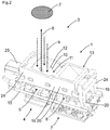
- einen optoelektronischen Sensor mit einer Leiterplatte und einem Spiegelträger;
- Figur 3
- den optoelektronischen Sensor aus
Figur 2 in einer Schnittdarstellung. - In den nachfolgenden Figuren sind identische Teile mit identischen Bezugszeichen versehen.
-
Figur 1 zeigt einen optoelektronischen Sensor 1 mit einem Gehäuse 21, einer Frontscheibe 22 und einem elektrischen Anschluss 23. - Bei dem optoelektronischen Sensor 1 handelt es sich bevorzugt um eine Lichtschranke, eine Reflexionslichtschranke, einen Lichttaster, oder einen Distanzsensor. Bei einer Reflexionslichtschranke sind Lichtsender bzw. Sendereinheit und Lichtempfänger bzw. Empfängereinheit auf der gleichen Seite eines Überwachungsbereiches, meist in einem einzigen Gehäuse untergebracht. Gegenüberliegend ist ein Retroreflektor angeordnet, der das vom Lichtsender ausgesandte Licht um 180° zurückreflektiert in den Lichtempfänger.
- Bei einem Lichttaster sind Lichtsender bzw. Sendereinheit und Lichtempfänger bzw. Empfängereinheit in einem gemeinsamen Gehäuse angeordnet. Die vom Lichtsender ausgesandten Lichtstrahlen werden an einem Objekt reflektiert oder remittiert.
-
Figur 2 zeigt den inneren Aufbau des optoelektronischen Sensors 1 ohne Gehäuse.Figur 2 zeigt einen optoelektronischen Sensor 1 zur Erkennung von Objekten 2 innerhalb eines Überwachungsbereichs 3, mit einer Sendereinheit 4 mit einem Sendeelement 5 zur Aussendung von Sendelichtstrahlen 6 in den Überwachungsbereich 3, und einer Empfängereinheit 7 mit einem Empfangselement 8 zum Empfang von Empfangslichtstrahlen 9 des Objektes 2, wobei die Empfängereinheit 7 mindestens ein Spiegelelement 10 aufweist zur Umlenkung der Empfangslichtstrahlen 9, wobei das Spiegelelement 10 aus amorphem Metall 11 gebildet ist. - Das Spiegelelement 10 ist beispielsweise vollständig durch ein spritzgussähnliches Verfahren hergestellt. Insbesondere kann bereits durch das Spritzgussbauteil ohne Nachbearbeitung eine hohe Oberflächengüte der Spiegeloberfläche bzw. des Spiegels 12 hergestellt bzw. bereitgestellt werden. Gemäß
Figur 2 ist das amorphe Metall 11 eine amorphe Metalllegierung. - Gemäß
Figur 2 ist ein definiertes elektrisches Potential mit dem Spiegelelement 10 verbunden. Das definierte elektrische Potential des optoelektronischen Sensors 1 ist ein elektrisches Potential, das mit der Leiterplatte 15 bzw. Elektronikkarte des optoelektronischen Sensors 1 verbunden ist. Das elektrische Potential ist beispielsweise von der Leiterplatte 15 über einen leitfähigen bzw. metallischen Kontakt oder einen metallischen Stift mit dem Spiegelelement verbunden. - Gemäß
Figur 2 ist der Spiegel 12 des Spiegelelements 10 konkav gekrümmt. Der Spiegel 12 ist somit nach innen gewölbt, wodurch ein Hohlspiegel gebildet ist. Dadurch können beispielsweise auf den Spiegel 12 fallende Empfangslichtstrahlen 9 durch den Spiegel 12 gebündelt bzw. fokussiert werden. - Gemäß
Figur 3 , welche eine Schnittdarstellung gemäßFigur 2 darstellt, ist ein zweiter Spiegel 12.1 des Spiegelelements 10.1 plan ausgebildet. - Gemäß
Figur 3 sind die Spiegelelemente 10, 10.1 in einem Spiegelträger 13 angeordnet, wobei die Spiegelelemente 10, 10.1 und der Spiegelträger 13 einstückig ausgebildet sind und aus amorphem Metall 11 bestehen. - Der Spiegelträger 13 bildet beispielsweise einen Rahmen für die Spiegelelemente 10, 10.1, wodurch die Spiegelelemente 10, 10.1 mechanisch stabiler ausgeführt sind. Dadurch ist eine besonders einfache, robuste und stabile Ausführung gewährleistet.
- Der Spiegelträger 13 gemäß
Figur 2 weist beispielsweise zusätzliche Seitenwände 24 auf. Weiter dient der Spiegelträger 13 als Befestigungsbasis für weitere Sensorkomponenten. Beispielsweise kann an dem Spiegelträger 13 eine Anschlusseinheit 25 befestigt werden. Der Spiegelträger 13 weist beispielsweise Befestigungsaufnahmen für ein Sensorgehäuse auf. Weiter kann der Spiegelträger 13 Referenzflächen zur Positionierung anderer Sensorkomponenten aufweisen. Weiter kann der Spiegelträger 13 Referenzflächen aufweisen, um den Spiegelträger 13 und damit die Spiegelelemente 10, 10.1 selbst gegenüber einer anderen Referenzfläche genau zu positionieren, um eine exakte Ausrichtung der Spiegelelemente 10, 10.1 zu gewährleisten. - Gemäß
Figur 2 weist der Spiegelträger 13 eine komplexe Struktur bzw. komplexe Oberfläche auf. Diese komplexe Struktur bzw. komplexe Oberfläche kann zur Befestigung dienen und kann an die Form anderer benachbarter Bauteile angepasst sein, so dass ein möglichst kompakter optoelektronischer Sensor 1 gebildet wird. - Gemäß
Figur 3 sind mindestens zwei Spiegelelemente 10, 10.1 und der Spiegelträger 13 einstückig ausgebildet. Dadurch können beispielsweise empfangene Lichtstrahlen durch die nacheinander angeordneten Spiegelelemente 10, 10.1 zweifach abgelenkt werden, um diese beispielsweise einem Empfangselement zuzuführen. Hierbei sind die jeweiligen Spiegelelemente 10, 10.1 unterschiedlich ausgebildet. Beispielsweise ist ein erstes Spiegelelement 10 konkav ausgebildet und ein zweites Spiegelelement 10.1 plan ausgebildet. - Gemäß
Figur 3 weist das Spiegelelement 10 eine Öffnung 14 für die Sendelichtstrahlen 6 auf. Dadurch kann beispielsweise in das Spiegelelement 10 für die Empfängereinheit 7 die Sendereinheit 4 mit dem Sendeelement 5 integriert werden. Insbesondere können die Sendelichtstrahlen 6 und die Empfangslichtstrahlen 9 kollimiert verlaufen. Bei der Öffnung 14 handelt es sich bevorzugt um eine runde Öffnung 14 bzw. ein Loch, welches beispielsweise nahe der Mitte oder mittig in dem Spiegelelement 10 angeordnet ist. - Gemäß
Figur 2 ist das Spiegelelement 10 bzw. der Spiegelträger 13 mit einer Leiterplatte 15 mechanisch verbunden. Beispielsweise sind auf der Leiterplatte 15 alle elektronischen Komponenten angeordnet und an dem Spiegelträger 13 alle optischen Komponenten angeordnet. Dadurch wird durch die mechanische Verbindung des Spiegelträgers 13 mit der Leiterplatte 15 der optoelektronische Sensor 1 nahezu komplett aufgebaut. Lediglich ein optionaler elektrischer Anschluss und das Sensorgehäuse müssen noch ergänzt werden, um einen einsatzfähigen optoelektronischen Sensor 1 zu erhalten. Beispielsweise ist das Sendeelement 5 und/oder das Empfangselement 8 und eine Auswerteeinheit auf der Leiterplatte 15 angeordnet. Die Leiterplatte weist optional mindestens eine Referenzfläche auf, die mit mindestens einer optionalen Referenzfläche des Spiegelträgers 13 verbunden wird. Dadurch wird das Sendelement 5 und das Empfangselement 8 zu dem Spiegelelement 10 ausgerichtet und referenziert. - Gemäß
Figur 3 weist der Spiegelträger 13 mindestens eine Aufnahme 16 für mindestens ein optisches Element 17 auf. Das optische Element 17 kann beispielsweise mindestens ein refraktives Element, beispielsweise mindestens eine Sammellinse 18 sein, Der Spiegelträger 13 weist wiederum Referenzflächen auf für das optische Element 17. - Gemäß
Figur 2 weist der Spiegelträger 13 zusätzlich zu den Spiegelelementen 10, 10.1 mindestens eine Fläche 19 auf, die einstückig zu dem Spiegelträger 13 ausgebildet ist, um eine EMV-Schirmfläche 20 zu bilden. Beispielsweise können mehrere Flächen 19 vorgesehen sein, die die Elektronik der Leiterplatte 15 abschirmen, so dass die Elektronik der Leiterplatte 15 abgeschirmt wird, wodurch der optoelektronische Sensor 1 eine bessere elektromagnetische Verträglichkeit aufweist. GemäßFigur 2 ist der Spiegelträger 13 bzw. die Spiegelelemente 10, 10.1 automatisiert auf einer Leiterplatte 15 bestückt. -
- 1 Optoelektronischer Sensor
- 2 Objekt
- 3 Überwachungsbereich
- 4 Sendereinheit
- 5 Sendeelement
- 6 Sendelichtstrahlen
- 7 Empfängereinheit
- 8 Empfangselement
- 9 Empfangslichtstrahlen
- 10,10.1 Spiegelelement
- 11 amorphes Metall
- 12, 12.1 Spiegel
- 13 Spiegelträger
- 14 Öffnung
- 15 Leiterplatte
- 16 Aufnahme
- 17 optisches Element
- 18 Sammellinse
- 19 Fläche
- 20 EMV-Schirmfläche
- 21 Gehäuse
- 22 Frontscheibe
- 23 Anschluss
- 24 Seitenwände
- 25 Anschlusseinheit
Claims (13)
- Optoelektronischer Sensor zur Erkennung von Objekten (2) innerhalb eines Überwachungsbereichs (3),
mit einer Sendereinheit (4) mit einem Sendeelement (5) zur Aussendung von Sendelichtstrahlen (6) in den Überwachungsbereich (3),
und/oder einer Empfängereinheit (7) mit einem Empfangselement (8) zum Empfang von Empfangslichtstrahlen (9) des Objektes (2),
wobei die Empfängereinheit (7) und/oder die Sendereinheit (4) mindestens ein Spiegelelement (10) aufweist zur Umlenkung der Lichtstrahlen (6, 9) dadurch gekennzeichnet, dass
das Spiegelelement (5) aus amorphem Metall (11) gebildet ist. - Optoelektronischer Sensor nach Anspruch 1, dadurch gekennzeichnet, dass das amorphe Metall (11) eine amorphe Metalllegierung ist.
- Optoelektronischer Sensor nach mindestens einem der vorhergehenden Ansprüche, dadurch gekennzeichnet, dass das Spiegelelement (10) mit einem definierten elektrischen Potential verbunden ist.
- Optoelektronischer Sensor nach mindestens einem der vorhergehenden Ansprüche, dadurch gekennzeichnet, dass der Spiegel (12) des Spiegelelements (5) konkav gekrümmt ist.
- Optoelektronischer Sensor nach mindestens einem der vorhergehenden Ansprüche, dadurch gekennzeichnet, dass der Spiegel (12) des Spiegelelements (5) plan ist.
- Optoelektronischer Sensor nach mindestens einem der vorhergehenden Ansprüche, dadurch gekennzeichnet, dass das Spiegelelement (5) in einem Spiegelträger (13) angeordnet ist, wobei das Spiegelelement (10) und der Spiegelträger (13) einstückig ausgebildet sind und aus amorphem Metall (11) bestehen.
- Optoelektronischer Sensor nach Anspruch 5, dadurch gekennzeichnet, dass mindestens zwei Spiegelelemente (10) und der Spiegelträger (13) einstückig ausgebildet sind.
- Optoelektronischer Sensor nach mindestens einem der vorhergehenden Ansprüche, dadurch gekennzeichnet, dass mindestens ein Spiegelelement (10) eine Öffnung (14) für die Sendelichtstrahlen (6) aufweist.
- Optoelektronischer Sensor nach mindestens einem der vorhergehenden Ansprüche 5 bis 7, dadurch gekennzeichnet, dass das Spiegelelement (10) oder der Spiegelträger (13) mit einer Leiterplatte (15) verbunden ist.
- Optoelektronischer Sensor nach mindestens einem der vorhergehenden Ansprüche 5 bis 8, dadurch gekennzeichnet, dass der Spiegelträger (13) mindestens eine Aufnahme (16) für mindestens ein optisches Element (17) aufweist.
- Optoelektronischer Sensor nach Anspruch 9, dadurch gekennzeichnet, dass das optische Element (17) eine Sammellinse (18) ist.
- Optoelektronischer Sensor nach mindestens einem der vorhergehenden Ansprüche 5 bis 10, dadurch gekennzeichnet, dass der Spiegelträger (13) zusätzlich zu dem Spiegelelement (10) mindestens eine Fläche (19) aufweist, die einstückig zu dem Spiegelträger (13) ausgebildet ist, um eine EMV-Schirmfläche (20) zu bilden.
- Optoelektronischer Sensor nach mindestens einem der vorhergehenden Ansprüche 8 bis 11, dadurch gekennzeichnet, dass das Spiegelelement (10) automatisiert auf einer Leiterplatte (15) bestückt ist.
Applications Claiming Priority (1)
| Application Number | Priority Date | Filing Date | Title |
|---|---|---|---|
| DE102016107153.6A DE102016107153B4 (de) | 2016-04-18 | 2016-04-18 | Optoelektronischer Sensor |
Publications (2)
| Publication Number | Publication Date |
|---|---|
| EP3236285A1 true EP3236285A1 (de) | 2017-10-25 |
| EP3236285B1 EP3236285B1 (de) | 2018-12-19 |
Family
ID=58412995
Family Applications (1)
| Application Number | Title | Priority Date | Filing Date |
|---|---|---|---|
| EP17162805.0A Active EP3236285B1 (de) | 2016-04-18 | 2017-03-24 | Optoelektronischer sensor |
Country Status (2)
| Country | Link |
|---|---|
| EP (1) | EP3236285B1 (de) |
| DE (1) | DE102016107153B4 (de) |
Families Citing this family (1)
| Publication number | Priority date | Publication date | Assignee | Title |
|---|---|---|---|---|
| DE102024131467A1 (de) * | 2024-10-29 | 2026-04-30 | Sick Ag | Optoelektronischer sensor zum erfassen von objekten |
Citations (8)
| Publication number | Priority date | Publication date | Assignee | Title |
|---|---|---|---|---|
| WO2006060081A2 (en) * | 2004-10-19 | 2006-06-08 | Liquidmetal Technologies, Inc. | Metallic mirrors formed from amorphous alloys |
| JP2006265050A (ja) * | 2005-03-24 | 2006-10-05 | Canon Inc | 光学素子成形型 |
| DE102005013317A1 (de) * | 2005-03-22 | 2006-10-05 | Leuze Electronic Gmbh & Co Kg | Optischer Sensor |
| US20100105980A1 (en) * | 2007-01-31 | 2010-04-29 | Namiki Seimitsu Houseki Kabushiki Kaisha | Motor and endoscope probe equipped with motor |
| DE202009007612U1 (de) * | 2009-05-28 | 2010-10-14 | Sick Ag | Reflexionslichtschrankensensor |
| JP2012113146A (ja) * | 2010-11-25 | 2012-06-14 | Canon Electronics Inc | 振動素子、光走査装置、アクチュエータ装置、映像投影装置及び画像形成装置 |
| DE202011052365U1 (de) * | 2011-12-20 | 2013-03-21 | Sick Ag | Reflexionslichtschranke |
| US20130139964A1 (en) * | 2011-11-16 | 2013-06-06 | California Institute Of Technology | Amorphous metals and composites as mirrors and mirror assemblies |
Family Cites Families (6)
| Publication number | Priority date | Publication date | Assignee | Title |
|---|---|---|---|---|
| DE952155C (de) * | 1954-05-23 | 1956-11-08 | Erwin Sick | Lichtelektrische Schranke |
| JP5203259B2 (ja) * | 2009-03-09 | 2013-06-05 | オリンパス株式会社 | 光学部品の製造方法 |
| DE102009051188A1 (de) * | 2009-10-29 | 2011-05-19 | Siemens Aktiengesellschaft | Lichtsignalgeber und Lichtempfänger für einen optischen Sensor |
| LU91714B1 (en) * | 2010-07-29 | 2012-01-30 | Iee Sarl | Active illumination scanning imager |
| JP6018926B2 (ja) * | 2013-01-09 | 2016-11-02 | 富士フイルム株式会社 | マイクロミラーデバイス及びその製造方法 |
| US20160223727A1 (en) * | 2013-09-18 | 2016-08-04 | Canon Kabushiki Kaisha | Optical unit, optical element and method for manufacturing the same |
-
2016
- 2016-04-18 DE DE102016107153.6A patent/DE102016107153B4/de not_active Expired - Fee Related
-
2017
- 2017-03-24 EP EP17162805.0A patent/EP3236285B1/de active Active
Patent Citations (8)
| Publication number | Priority date | Publication date | Assignee | Title |
|---|---|---|---|---|
| WO2006060081A2 (en) * | 2004-10-19 | 2006-06-08 | Liquidmetal Technologies, Inc. | Metallic mirrors formed from amorphous alloys |
| DE102005013317A1 (de) * | 2005-03-22 | 2006-10-05 | Leuze Electronic Gmbh & Co Kg | Optischer Sensor |
| JP2006265050A (ja) * | 2005-03-24 | 2006-10-05 | Canon Inc | 光学素子成形型 |
| US20100105980A1 (en) * | 2007-01-31 | 2010-04-29 | Namiki Seimitsu Houseki Kabushiki Kaisha | Motor and endoscope probe equipped with motor |
| DE202009007612U1 (de) * | 2009-05-28 | 2010-10-14 | Sick Ag | Reflexionslichtschrankensensor |
| JP2012113146A (ja) * | 2010-11-25 | 2012-06-14 | Canon Electronics Inc | 振動素子、光走査装置、アクチュエータ装置、映像投影装置及び画像形成装置 |
| US20130139964A1 (en) * | 2011-11-16 | 2013-06-06 | California Institute Of Technology | Amorphous metals and composites as mirrors and mirror assemblies |
| DE202011052365U1 (de) * | 2011-12-20 | 2013-03-21 | Sick Ag | Reflexionslichtschranke |
Also Published As
| Publication number | Publication date |
|---|---|
| DE102016107153B4 (de) | 2018-10-18 |
| EP3236285B1 (de) | 2018-12-19 |
| DE102016107153A1 (de) | 2017-10-19 |
Similar Documents
| Publication | Publication Date | Title |
|---|---|---|
| EP1058142A2 (de) | Laserscanner mit kugelförmigen Linse | |
| DE102011113172A1 (de) | Optoelektronisches Bauelement | |
| EP1929329B1 (de) | Elektro-optisches messgerät | |
| DE10331074A1 (de) | Sensoranordnung zur Abstands- und/oder Geschwindigkeitsmessung | |
| EP3388857B1 (de) | Laserscanner und verfahren zur überprüfung der funktionsfähigkeit | |
| EP1845334A1 (de) | Optischer Sensor | |
| EP3236285B1 (de) | Optoelektronischer sensor | |
| DE10308085B4 (de) | Optoelektronische Vorrichtung | |
| DE10201746A1 (de) | Optoelektronische Vorrichtung | |
| DE202016102035U1 (de) | Optoelektronischer Sensor | |
| EP1624322A1 (de) | Optischer Sensor | |
| EP1102086B1 (de) | Optoelektronische Vorrichtung | |
| EP3907547A1 (de) | Optoelektronischer sensor | |
| DE202019106231U1 (de) | Rotationsfähiger optischer Kurzstrecken-Transceiver | |
| DE29620422U1 (de) | Optoelektronischer Sensor mit in einem Gehäusegrundkörper integrierten Haltevorrichtungen | |
| DE102016121913A1 (de) | Mehrstrahllichtschranke | |
| DE2946111A1 (de) | Optischer koerper fuer ein lidar-system | |
| EP1760509A2 (de) | Verfahren zur Justage eines abbildenden Elements sowie Messgerät justiert nach einem derartigen Verfahren | |
| DE102008056071B4 (de) | Optischer Sensor zur Objektdetektion | |
| DE19844238C2 (de) | Optoelektronische Vorrichtung | |
| DE202020102514U1 (de) | Optoelektronischer Sensor | |
| EP3312760B1 (de) | Optischer sensor | |
| EP1341118B1 (de) | Optoelektronische Vorrichtung | |
| EP4369031B1 (de) | Optoelektronischer sensor | |
| DE202016106394U1 (de) | Mehrstrahllichtschranke |
Legal Events
| Date | Code | Title | Description |
|---|---|---|---|
| PUAI | Public reference made under article 153(3) epc to a published international application that has entered the european phase |
Free format text: ORIGINAL CODE: 0009012 |
|
| STAA | Information on the status of an ep patent application or granted ep patent |
Free format text: STATUS: THE APPLICATION HAS BEEN PUBLISHED |
|
| AK | Designated contracting states |
Kind code of ref document: A1 Designated state(s): AL AT BE BG CH CY CZ DE DK EE ES FI FR GB GR HR HU IE IS IT LI LT LU LV MC MK MT NL NO PL PT RO RS SE SI SK SM TR |
|
| AX | Request for extension of the european patent |
Extension state: BA ME |
|
| STAA | Information on the status of an ep patent application or granted ep patent |
Free format text: STATUS: REQUEST FOR EXAMINATION WAS MADE |
|
| 17P | Request for examination filed |
Effective date: 20180216 |
|
| RBV | Designated contracting states (corrected) |
Designated state(s): AL AT BE BG CH CY CZ DE DK EE ES FI FR GB GR HR HU IE IS IT LI LT LU LV MC MK MT NL NO PL PT RO RS SE SI SK SM TR |
|
| REG | Reference to a national code |
Ref country code: DE Ref legal event code: R079 Ref document number: 502017000523 Country of ref document: DE Free format text: PREVIOUS MAIN CLASS: G01S0017020000 Ipc: G02B0005080000 |
|
| RIC1 | Information provided on ipc code assigned before grant |
Ipc: G01V 8/14 20060101ALI20180417BHEP Ipc: G02B 5/08 20060101AFI20180417BHEP Ipc: G01S 17/48 20060101ALI20180417BHEP Ipc: B29D 11/00 20060101ALI20180417BHEP Ipc: G01S 17/02 20060101ALI20180417BHEP Ipc: G01S 17/08 20060101ALI20180417BHEP Ipc: G01S 7/481 20060101ALI20180417BHEP |
|
| GRAP | Despatch of communication of intention to grant a patent |
Free format text: ORIGINAL CODE: EPIDOSNIGR1 |
|
| STAA | Information on the status of an ep patent application or granted ep patent |
Free format text: STATUS: GRANT OF PATENT IS INTENDED |
|
| INTG | Intention to grant announced |
Effective date: 20180528 |
|
| GRAJ | Information related to disapproval of communication of intention to grant by the applicant or resumption of examination proceedings by the epo deleted |
Free format text: ORIGINAL CODE: EPIDOSDIGR1 |
|
| STAA | Information on the status of an ep patent application or granted ep patent |
Free format text: STATUS: REQUEST FOR EXAMINATION WAS MADE |
|
| GRAP | Despatch of communication of intention to grant a patent |
Free format text: ORIGINAL CODE: EPIDOSNIGR1 |
|
| STAA | Information on the status of an ep patent application or granted ep patent |
Free format text: STATUS: GRANT OF PATENT IS INTENDED |
|
| INTC | Intention to grant announced (deleted) | ||
| GRAJ | Information related to disapproval of communication of intention to grant by the applicant or resumption of examination proceedings by the epo deleted |
Free format text: ORIGINAL CODE: EPIDOSDIGR1 |
|
| STAA | Information on the status of an ep patent application or granted ep patent |
Free format text: STATUS: REQUEST FOR EXAMINATION WAS MADE |
|
| INTG | Intention to grant announced |
Effective date: 20180925 |
|
| GRAP | Despatch of communication of intention to grant a patent |
Free format text: ORIGINAL CODE: EPIDOSNIGR1 |
|
| STAA | Information on the status of an ep patent application or granted ep patent |
Free format text: STATUS: GRANT OF PATENT IS INTENDED |
|
| GRAS | Grant fee paid |
Free format text: ORIGINAL CODE: EPIDOSNIGR3 |
|
| INTC | Intention to grant announced (deleted) | ||
| GRAA | (expected) grant |
Free format text: ORIGINAL CODE: 0009210 |
|
| STAA | Information on the status of an ep patent application or granted ep patent |
Free format text: STATUS: THE PATENT HAS BEEN GRANTED |
|
| INTG | Intention to grant announced |
Effective date: 20181031 |
|
| AK | Designated contracting states |
Kind code of ref document: B1 Designated state(s): AL AT BE BG CH CY CZ DE DK EE ES FI FR GB GR HR HU IE IS IT LI LT LU LV MC MK MT NL NO PL PT RO RS SE SI SK SM TR |
|
| REG | Reference to a national code |
Ref country code: GB Ref legal event code: FG4D Free format text: NOT ENGLISH |
|
| REG | Reference to a national code |
Ref country code: CH Ref legal event code: EP |
|
| REG | Reference to a national code |
Ref country code: IE Ref legal event code: FG4D Free format text: LANGUAGE OF EP DOCUMENT: GERMAN |
|
| REG | Reference to a national code |
Ref country code: DE Ref legal event code: R096 Ref document number: 502017000523 Country of ref document: DE |
|
| REG | Reference to a national code |
Ref country code: AT Ref legal event code: REF Ref document number: 1079311 Country of ref document: AT Kind code of ref document: T Effective date: 20190115 |
|
| REG | Reference to a national code |
Ref country code: NL Ref legal event code: MP Effective date: 20181219 |
|
| PG25 | Lapsed in a contracting state [announced via postgrant information from national office to epo] |
Ref country code: LV Free format text: LAPSE BECAUSE OF FAILURE TO SUBMIT A TRANSLATION OF THE DESCRIPTION OR TO PAY THE FEE WITHIN THE PRESCRIBED TIME-LIMIT Effective date: 20181219 Ref country code: HR Free format text: LAPSE BECAUSE OF FAILURE TO SUBMIT A TRANSLATION OF THE DESCRIPTION OR TO PAY THE FEE WITHIN THE PRESCRIBED TIME-LIMIT Effective date: 20181219 Ref country code: BG Free format text: LAPSE BECAUSE OF FAILURE TO SUBMIT A TRANSLATION OF THE DESCRIPTION OR TO PAY THE FEE WITHIN THE PRESCRIBED TIME-LIMIT Effective date: 20190319 Ref country code: NO Free format text: LAPSE BECAUSE OF FAILURE TO SUBMIT A TRANSLATION OF THE DESCRIPTION OR TO PAY THE FEE WITHIN THE PRESCRIBED TIME-LIMIT Effective date: 20190319 Ref country code: FI Free format text: LAPSE BECAUSE OF FAILURE TO SUBMIT A TRANSLATION OF THE DESCRIPTION OR TO PAY THE FEE WITHIN THE PRESCRIBED TIME-LIMIT Effective date: 20181219 Ref country code: LT Free format text: LAPSE BECAUSE OF FAILURE TO SUBMIT A TRANSLATION OF THE DESCRIPTION OR TO PAY THE FEE WITHIN THE PRESCRIBED TIME-LIMIT Effective date: 20181219 |
|
| REG | Reference to a national code |
Ref country code: LT Ref legal event code: MG4D |
|
| PG25 | Lapsed in a contracting state [announced via postgrant information from national office to epo] |
Ref country code: SE Free format text: LAPSE BECAUSE OF FAILURE TO SUBMIT A TRANSLATION OF THE DESCRIPTION OR TO PAY THE FEE WITHIN THE PRESCRIBED TIME-LIMIT Effective date: 20181219 Ref country code: RS Free format text: LAPSE BECAUSE OF FAILURE TO SUBMIT A TRANSLATION OF THE DESCRIPTION OR TO PAY THE FEE WITHIN THE PRESCRIBED TIME-LIMIT Effective date: 20181219 Ref country code: AL Free format text: LAPSE BECAUSE OF FAILURE TO SUBMIT A TRANSLATION OF THE DESCRIPTION OR TO PAY THE FEE WITHIN THE PRESCRIBED TIME-LIMIT Effective date: 20181219 Ref country code: GR Free format text: LAPSE BECAUSE OF FAILURE TO SUBMIT A TRANSLATION OF THE DESCRIPTION OR TO PAY THE FEE WITHIN THE PRESCRIBED TIME-LIMIT Effective date: 20190320 |
|
| PG25 | Lapsed in a contracting state [announced via postgrant information from national office to epo] |
Ref country code: NL Free format text: LAPSE BECAUSE OF FAILURE TO SUBMIT A TRANSLATION OF THE DESCRIPTION OR TO PAY THE FEE WITHIN THE PRESCRIBED TIME-LIMIT Effective date: 20181219 |
|
| PG25 | Lapsed in a contracting state [announced via postgrant information from national office to epo] |
Ref country code: PT Free format text: LAPSE BECAUSE OF FAILURE TO SUBMIT A TRANSLATION OF THE DESCRIPTION OR TO PAY THE FEE WITHIN THE PRESCRIBED TIME-LIMIT Effective date: 20190419 Ref country code: ES Free format text: LAPSE BECAUSE OF FAILURE TO SUBMIT A TRANSLATION OF THE DESCRIPTION OR TO PAY THE FEE WITHIN THE PRESCRIBED TIME-LIMIT Effective date: 20181219 Ref country code: CZ Free format text: LAPSE BECAUSE OF FAILURE TO SUBMIT A TRANSLATION OF THE DESCRIPTION OR TO PAY THE FEE WITHIN THE PRESCRIBED TIME-LIMIT Effective date: 20181219 Ref country code: PL Free format text: LAPSE BECAUSE OF FAILURE TO SUBMIT A TRANSLATION OF THE DESCRIPTION OR TO PAY THE FEE WITHIN THE PRESCRIBED TIME-LIMIT Effective date: 20181219 |
|
| PG25 | Lapsed in a contracting state [announced via postgrant information from national office to epo] |
Ref country code: IS Free format text: LAPSE BECAUSE OF FAILURE TO SUBMIT A TRANSLATION OF THE DESCRIPTION OR TO PAY THE FEE WITHIN THE PRESCRIBED TIME-LIMIT Effective date: 20190419 Ref country code: SM Free format text: LAPSE BECAUSE OF FAILURE TO SUBMIT A TRANSLATION OF THE DESCRIPTION OR TO PAY THE FEE WITHIN THE PRESCRIBED TIME-LIMIT Effective date: 20181219 Ref country code: SK Free format text: LAPSE BECAUSE OF FAILURE TO SUBMIT A TRANSLATION OF THE DESCRIPTION OR TO PAY THE FEE WITHIN THE PRESCRIBED TIME-LIMIT Effective date: 20181219 Ref country code: EE Free format text: LAPSE BECAUSE OF FAILURE TO SUBMIT A TRANSLATION OF THE DESCRIPTION OR TO PAY THE FEE WITHIN THE PRESCRIBED TIME-LIMIT Effective date: 20181219 Ref country code: RO Free format text: LAPSE BECAUSE OF FAILURE TO SUBMIT A TRANSLATION OF THE DESCRIPTION OR TO PAY THE FEE WITHIN THE PRESCRIBED TIME-LIMIT Effective date: 20181219 |
|
| REG | Reference to a national code |
Ref country code: DE Ref legal event code: R097 Ref document number: 502017000523 Country of ref document: DE |
|
| PLBE | No opposition filed within time limit |
Free format text: ORIGINAL CODE: 0009261 |
|
| STAA | Information on the status of an ep patent application or granted ep patent |
Free format text: STATUS: NO OPPOSITION FILED WITHIN TIME LIMIT |
|
| PG25 | Lapsed in a contracting state [announced via postgrant information from national office to epo] |
Ref country code: MC Free format text: LAPSE BECAUSE OF FAILURE TO SUBMIT A TRANSLATION OF THE DESCRIPTION OR TO PAY THE FEE WITHIN THE PRESCRIBED TIME-LIMIT Effective date: 20181219 Ref country code: DK Free format text: LAPSE BECAUSE OF FAILURE TO SUBMIT A TRANSLATION OF THE DESCRIPTION OR TO PAY THE FEE WITHIN THE PRESCRIBED TIME-LIMIT Effective date: 20181219 |
|
| 26N | No opposition filed |
Effective date: 20190920 |
|
| PG25 | Lapsed in a contracting state [announced via postgrant information from national office to epo] |
Ref country code: LU Free format text: LAPSE BECAUSE OF NON-PAYMENT OF DUE FEES Effective date: 20190324 |
|
| REG | Reference to a national code |
Ref country code: BE Ref legal event code: MM Effective date: 20190331 |
|
| PG25 | Lapsed in a contracting state [announced via postgrant information from national office to epo] |
Ref country code: IE Free format text: LAPSE BECAUSE OF NON-PAYMENT OF DUE FEES Effective date: 20190324 |
|
| PG25 | Lapsed in a contracting state [announced via postgrant information from national office to epo] |
Ref country code: BE Free format text: LAPSE BECAUSE OF NON-PAYMENT OF DUE FEES Effective date: 20190331 Ref country code: SI Free format text: LAPSE BECAUSE OF FAILURE TO SUBMIT A TRANSLATION OF THE DESCRIPTION OR TO PAY THE FEE WITHIN THE PRESCRIBED TIME-LIMIT Effective date: 20181219 |
|
| PG25 | Lapsed in a contracting state [announced via postgrant information from national office to epo] |
Ref country code: TR Free format text: LAPSE BECAUSE OF FAILURE TO SUBMIT A TRANSLATION OF THE DESCRIPTION OR TO PAY THE FEE WITHIN THE PRESCRIBED TIME-LIMIT Effective date: 20181219 |
|
| PG25 | Lapsed in a contracting state [announced via postgrant information from national office to epo] |
Ref country code: MT Free format text: LAPSE BECAUSE OF FAILURE TO SUBMIT A TRANSLATION OF THE DESCRIPTION OR TO PAY THE FEE WITHIN THE PRESCRIBED TIME-LIMIT Effective date: 20181219 |
|
| REG | Reference to a national code |
Ref country code: CH Ref legal event code: PL |
|
| PG25 | Lapsed in a contracting state [announced via postgrant information from national office to epo] |
Ref country code: CH Free format text: LAPSE BECAUSE OF NON-PAYMENT OF DUE FEES Effective date: 20200331 Ref country code: LI Free format text: LAPSE BECAUSE OF NON-PAYMENT OF DUE FEES Effective date: 20200331 |
|
| PG25 | Lapsed in a contracting state [announced via postgrant information from national office to epo] |
Ref country code: CY Free format text: LAPSE BECAUSE OF FAILURE TO SUBMIT A TRANSLATION OF THE DESCRIPTION OR TO PAY THE FEE WITHIN THE PRESCRIBED TIME-LIMIT Effective date: 20181219 |
|
| PG25 | Lapsed in a contracting state [announced via postgrant information from national office to epo] |
Ref country code: HU Free format text: LAPSE BECAUSE OF FAILURE TO SUBMIT A TRANSLATION OF THE DESCRIPTION OR TO PAY THE FEE WITHIN THE PRESCRIBED TIME-LIMIT; INVALID AB INITIO Effective date: 20170324 |
|
| GBPC | Gb: european patent ceased through non-payment of renewal fee |
Effective date: 20210324 |
|
| PG25 | Lapsed in a contracting state [announced via postgrant information from national office to epo] |
Ref country code: GB Free format text: LAPSE BECAUSE OF NON-PAYMENT OF DUE FEES Effective date: 20210324 |
|
| PG25 | Lapsed in a contracting state [announced via postgrant information from national office to epo] |
Ref country code: MK Free format text: LAPSE BECAUSE OF FAILURE TO SUBMIT A TRANSLATION OF THE DESCRIPTION OR TO PAY THE FEE WITHIN THE PRESCRIBED TIME-LIMIT Effective date: 20181219 |
|
| PGFP | Annual fee paid to national office [announced via postgrant information from national office to epo] |
Ref country code: AT Payment date: 20250319 Year of fee payment: 9 |
|
| PGFP | Annual fee paid to national office [announced via postgrant information from national office to epo] |
Ref country code: IT Payment date: 20250331 Year of fee payment: 9 |
|
| PGFP | Annual fee paid to national office [announced via postgrant information from national office to epo] |
Ref country code: DE Payment date: 20260320 Year of fee payment: 10 |
|
| PGFP | Annual fee paid to national office [announced via postgrant information from national office to epo] |
Ref country code: FR Payment date: 20260324 Year of fee payment: 10 |