EP3235136B1 - Étalonnage d'oscillateur - Google Patents
Étalonnage d'oscillateur Download PDFInfo
- Publication number
- EP3235136B1 EP3235136B1 EP15813517.8A EP15813517A EP3235136B1 EP 3235136 B1 EP3235136 B1 EP 3235136B1 EP 15813517 A EP15813517 A EP 15813517A EP 3235136 B1 EP3235136 B1 EP 3235136B1
- Authority
- EP
- European Patent Office
- Prior art keywords
- locked loop
- phase locked
- calibration
- frequency
- mode
- Prior art date
- Legal status (The legal status is an assumption and is not a legal conclusion. Google has not performed a legal analysis and makes no representation as to the accuracy of the status listed.)
- Active
Links
- 238000007493 shaping process Methods 0.000 claims description 5
- 230000007704 transition Effects 0.000 claims description 3
- 230000001960 triggered effect Effects 0.000 claims 1
- 230000035945 sensitivity Effects 0.000 description 4
- 238000000034 method Methods 0.000 description 2
- 239000003990 capacitor Substances 0.000 description 1
- 239000013078 crystal Substances 0.000 description 1
- 238000010586 diagram Methods 0.000 description 1
- 230000001360 synchronised effect Effects 0.000 description 1
Images
Classifications
-
- H—ELECTRICITY
- H03—ELECTRONIC CIRCUITRY
- H03L—AUTOMATIC CONTROL, STARTING, SYNCHRONISATION, OR STABILISATION OF GENERATORS OF ELECTRONIC OSCILLATIONS OR PULSES
- H03L7/00—Automatic control of frequency or phase; Synchronisation
- H03L7/06—Automatic control of frequency or phase; Synchronisation using a reference signal applied to a frequency- or phase-locked loop
- H03L7/16—Indirect frequency synthesis, i.e. generating a desired one of a number of predetermined frequencies using a frequency- or phase-locked loop
- H03L7/18—Indirect frequency synthesis, i.e. generating a desired one of a number of predetermined frequencies using a frequency- or phase-locked loop using a frequency divider or counter in the loop
- H03L7/183—Indirect frequency synthesis, i.e. generating a desired one of a number of predetermined frequencies using a frequency- or phase-locked loop using a frequency divider or counter in the loop a time difference being used for locking the loop, the counter counting between fixed numbers or the frequency divider dividing by a fixed number
- H03L7/187—Indirect frequency synthesis, i.e. generating a desired one of a number of predetermined frequencies using a frequency- or phase-locked loop using a frequency divider or counter in the loop a time difference being used for locking the loop, the counter counting between fixed numbers or the frequency divider dividing by a fixed number using means for coarse tuning the voltage controlled oscillator of the loop
-
- H—ELECTRICITY
- H03—ELECTRONIC CIRCUITRY
- H03L—AUTOMATIC CONTROL, STARTING, SYNCHRONISATION, OR STABILISATION OF GENERATORS OF ELECTRONIC OSCILLATIONS OR PULSES
- H03L7/00—Automatic control of frequency or phase; Synchronisation
- H03L7/06—Automatic control of frequency or phase; Synchronisation using a reference signal applied to a frequency- or phase-locked loop
- H03L7/16—Indirect frequency synthesis, i.e. generating a desired one of a number of predetermined frequencies using a frequency- or phase-locked loop
- H03L7/18—Indirect frequency synthesis, i.e. generating a desired one of a number of predetermined frequencies using a frequency- or phase-locked loop using a frequency divider or counter in the loop
- H03L7/197—Indirect frequency synthesis, i.e. generating a desired one of a number of predetermined frequencies using a frequency- or phase-locked loop using a frequency divider or counter in the loop a time difference being used for locking the loop, the counter counting between numbers which are variable in time or the frequency divider dividing by a factor variable in time, e.g. for obtaining fractional frequency division
- H03L7/1974—Indirect frequency synthesis, i.e. generating a desired one of a number of predetermined frequencies using a frequency- or phase-locked loop using a frequency divider or counter in the loop a time difference being used for locking the loop, the counter counting between numbers which are variable in time or the frequency divider dividing by a factor variable in time, e.g. for obtaining fractional frequency division for fractional frequency division
- H03L7/1976—Indirect frequency synthesis, i.e. generating a desired one of a number of predetermined frequencies using a frequency- or phase-locked loop using a frequency divider or counter in the loop a time difference being used for locking the loop, the counter counting between numbers which are variable in time or the frequency divider dividing by a factor variable in time, e.g. for obtaining fractional frequency division for fractional frequency division using a phase accumulator for controlling the counter or frequency divider
-
- H—ELECTRICITY
- H03—ELECTRONIC CIRCUITRY
- H03L—AUTOMATIC CONTROL, STARTING, SYNCHRONISATION, OR STABILISATION OF GENERATORS OF ELECTRONIC OSCILLATIONS OR PULSES
- H03L7/00—Automatic control of frequency or phase; Synchronisation
- H03L7/06—Automatic control of frequency or phase; Synchronisation using a reference signal applied to a frequency- or phase-locked loop
- H03L7/08—Details of the phase-locked loop
- H03L7/085—Details of the phase-locked loop concerning mainly the frequency- or phase-detection arrangement including the filtering or amplification of its output signal
-
- H—ELECTRICITY
- H03—ELECTRONIC CIRCUITRY
- H03L—AUTOMATIC CONTROL, STARTING, SYNCHRONISATION, OR STABILISATION OF GENERATORS OF ELECTRONIC OSCILLATIONS OR PULSES
- H03L7/00—Automatic control of frequency or phase; Synchronisation
- H03L7/06—Automatic control of frequency or phase; Synchronisation using a reference signal applied to a frequency- or phase-locked loop
- H03L7/08—Details of the phase-locked loop
- H03L7/099—Details of the phase-locked loop concerning mainly the controlled oscillator of the loop
- H03L7/0991—Details of the phase-locked loop concerning mainly the controlled oscillator of the loop the oscillator being a digital oscillator, e.g. composed of a fixed oscillator followed by a variable frequency divider
- H03L7/0992—Details of the phase-locked loop concerning mainly the controlled oscillator of the loop the oscillator being a digital oscillator, e.g. composed of a fixed oscillator followed by a variable frequency divider comprising a counter or a frequency divider
-
- H—ELECTRICITY
- H03—ELECTRONIC CIRCUITRY
- H03L—AUTOMATIC CONTROL, STARTING, SYNCHRONISATION, OR STABILISATION OF GENERATORS OF ELECTRONIC OSCILLATIONS OR PULSES
- H03L7/00—Automatic control of frequency or phase; Synchronisation
- H03L7/06—Automatic control of frequency or phase; Synchronisation using a reference signal applied to a frequency- or phase-locked loop
- H03L7/16—Indirect frequency synthesis, i.e. generating a desired one of a number of predetermined frequencies using a frequency- or phase-locked loop
- H03L7/18—Indirect frequency synthesis, i.e. generating a desired one of a number of predetermined frequencies using a frequency- or phase-locked loop using a frequency divider or counter in the loop
- H03L7/197—Indirect frequency synthesis, i.e. generating a desired one of a number of predetermined frequencies using a frequency- or phase-locked loop using a frequency divider or counter in the loop a time difference being used for locking the loop, the counter counting between numbers which are variable in time or the frequency divider dividing by a factor variable in time, e.g. for obtaining fractional frequency division
-
- H—ELECTRICITY
- H03—ELECTRONIC CIRCUITRY
- H03M—CODING; DECODING; CODE CONVERSION IN GENERAL
- H03M3/00—Conversion of analogue values to or from differential modulation
- H03M3/30—Delta-sigma modulation
-
- H—ELECTRICITY
- H04—ELECTRIC COMMUNICATION TECHNIQUE
- H04B—TRANSMISSION
- H04B1/00—Details of transmission systems, not covered by a single one of groups H04B3/00 - H04B13/00; Details of transmission systems not characterised by the medium used for transmission
- H04B1/38—Transceivers, i.e. devices in which transmitter and receiver form a structural unit and in which at least one part is used for functions of transmitting and receiving
- H04B1/40—Circuits
Definitions
- This invention relates to the calibration of oscillators, particularly although not exclusively tuning the voltage controlled oscillator of a phase-locked loop used in a frequency synthesizer. e.g. for tuning applications in digital radio transmitters and receivers.
- Voltage controlled oscillators VCOs
- PLLs phase locked loops
- a problem with VCOs which has been appreciated by the Applicant is that when they are used in PLLs which form part of frequency synthesizers for digital radio applications, they are required to operate over a relatively large frequency range - e.g. of the order of hundreds of MHz This frequency tuning range may need to be accommodated within a voltage swing of only 0.6V which means the VCO needs to have a very high gain and thus will be sensitive to loop filter noise.
- Typical VCOs also exhibit lots of variation: for example their capacitance may vary by as much as 15% which leads to a change in the centre frequency.
- US 2013/0278303 discloses a PLL comprising a VCO, where the VCO can be controlled by a coarse tuning signal and/or a fine tuning signal.
- US 2013/0069696 also discloses a PLL comprising a VCO, variable divider arrangement, a sigma-delta modulator and a phase detector. The present invention aims to provide a different approach. When viewed from a first aspect the invention provides a phase locked loop as claimed in claim 1.
- controllable oscillator can be controlled digitally by the calibration module in the calibration mode. This allows for a coarse tuning to be effected so that voltage control of the output frequency only needs to be used for fine tuning within a small subset of the overall frequency range. This in turn means that the sensitivity of the controllable oscillator can be significantly reduced which reduces the problem of noise.
- the sigma-delta modulator operating during the calibration mode ensures that adequate resolution is available in the control which can be asserted over the controllable oscillator but in a set of embodiments the sigma-delta modulator is arranged to operate in a different mode during said calibration mode than during said normal mode.
- the sigma-delta modulator is arranged to operate with second order multi-stage noise shaping (MASH), e.g. MASH 1-1 in said calibration mode and with third order multi-stage noise shaping, e.g. MASH 1-1-1 in said normal mode.
- MASH multi-stage noise shaping
- the calibration module could be arranged to determine whether the controllable oscillator is running too fast or too slow at a given point during calibrations and thus whether a digital calibration signal output from the calibration module is required to increase or decrease the frequency of the controllable oscillator.
- a digital calibration signal output from the calibration module is required to increase or decrease the frequency of the controllable oscillator.
- the Applicant has appreciated that such an arrangement would require a data bus extending between the divider arrangement and the calibration module which would therefore need to span the different clock regimes between these two.
- the Applicant has addressed this by arranging for the divider arrangement to count pulses from the controllable oscillator and to output a signal to the calibration module indicating whether the oscillator is running too fast or too slow. This avoids any need to cross clock domains as it permits a single line interface rather than a data bus.
- the divider arrangement is arranged to determine a state of a counter contained therein when a next transition edge is received from the reference clock and to determine on the basis of said counter state whether the controllable oscillator frequency is too high or too low.
- the PLL is a fractional N PLL - that is the division factor applied can be varied to give an exact desired frequency.
- the divider arrangement comprises a variable modulus prescaler (VMP).
- VMP variable modulus prescaler
- the divider arrangement may rely just on the VMP but in a set of embodiments a further divider is also provided.
- the further divider could be fixed but in a set of embodiments it may be changed to change to a different loop frequency.
- the PLL is arranged to enter said calibration mode whenever a reset is required.
- it may be arranged to enter said calibration mode whenever a new data packet is transmitted or received, when the transmitter or receiver is arranged to operate on a different frequency channel or when a system changes operation mode from receive to transmit or vice versa.
- the calibration module is arranged to perform a binary search for a digitally-optimised calibration. This means that a plurality of bits, e.g. of reducing significance, are established. In an exemplary set of embodiments a five bit word is used. This means that there are 32 possible digital tuning calibrations for the PLL so that the voltage control of the frequency need only vary the frequency over 1 ⁇ 32 of the entire range giving a big decrease in the sensitivity of the controllable oscillator (although in practice the bands will typically overlap).
- the calibration module preferably comprises a finite state machine.
- phase locked loop is used in a frequency synthesizer of a digital radio transmitter or receiver.
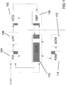
- FIG. 1 is a schematic diagram of a phase locked loop embodying the invention.
- a fractional N phase locked-loop (PLL) embodying the invention is shown in Fig. 1 .
- VCO voltage controlled oscillator
- phase detector 104 causes small adjustments to the frequency of the VCO 102 in order to bring the phase (and therefore frequency) of the fed-back signal into alignment with the reference clock CK_REF.
- the frequency of the VCO 102 is therefore controlled to be F ref *N*(nP+m(P+1)) where F ref is the reference crystal frequency and n and m are the relative proportions of the occurrences of the respective counts P and P+1 over a given time period.
- the divider module 110 is controlled by a sigma-delta modulator (SDM) 112 to determine the above-mentioned N and relative proportions of P and P+1 counts, so determining the precise frequency.
- SDM sigma-delta modulator
- the precisely divided average frequency signal is fed to the phase detector 104 which generates an output signal to control the VCO 102 in accordance with any mismatch between the signal from the divider 110 and the reference clock input signal CK_REF.
- a finite state machine (FSM) 114. This takes an input from the DIVN divider module 110 and provides output signals to the controllable oscillator 102, phase detector 104, SDM 112 and DIVN module 110.
- FSM finite state machine
- the frequency of the VCO 102 is controlled by changes in a voltage signal from the phase detector 104 via the low pass filter 106. This In turn is controlled by the output from the sigma-delta modulator 112 which exerts influence over the variable modulator pre-scaler 108 and the DIVN module 110.
- the overall frequency division is thus split between two modules.
- the pre-scaler 108 has a variable modulus so that it can divide by P or P+1 depending on the control signal from the DIVN 110 which allows for the full range of fractional counts.
- the pre-scaler 108 could be an asynchronous or ripple counter but this is not essential.
- the DIVN module 110 is a counter, which may be a synchronous counter that operates on the divided clock and divides by an amount N determined by its control input.
- the resulting frequency division can therefore be expressed as N*P + A where A represents how many times during one output cycle the VMP 108 has divided by P+1.
- the input clock for the VMP 108 is provided by the output of the VCO 102.
- the VMP 108 produces an intermediate clock which is passed to the DIVN module 110.
- the output from the DIVN module 110 is a clock signal CK_O1 which is passed to the phase detector 104.
- the VCO is not controlled across the entire frequency range which the PLL is able to produce. Instead its frequency can only be varied by means of the voltage applied to it within a relatively narrow frequency band.
- a digital tuning is applied during a calibration mode.
- the FSM issues control signals which cause the frequency of the VCO 102 no longer to be controlled by the output signal voltage of the phase detector 103 by fixing its output signal voltage. Rather in this mode the controllable oscillator 102 is controlled directly by the FSM 114 which can generate appropriate binary control words to set the frequency of the VCO 102.
- the control word signals are used to switch capacitors in or out of circuit in the VCO 102 in order to alter its baseline frequency.
- the FSM 114 generates a 5-bit control word to the VCO 102 and undertakes a 5-cycle binary search for the control word which most closely matches the desired frequency, from the most to least significant bit.
- one bit of the tuning word is determined by the DIVN module 110 which monitors the state of its counter as compared to a predetermined expected state when a transition edge is received on the reference clock input CK_REF. If the count is too high the VCO is determined to be running too fast and if it is too low the VCO is determined to be running too low.
- the DIVN module 110 issues a single bit output to the FSM 114 which uses this to set the control word bit appropriately to set the frequency band of the VCO 102.
- the count determination is carried out by the divider module 110 itself, rather than the FSM 114, it is not necessary to provide a data bus crossing the respective clock domains, substantially simplifying the circuit.
- the sigma-delta modulator 112 must continue to be operated to ensure that the division factor applied by the divider arrangement 108, 110 (i.e. the values of N and A in the description above) can be altered which gives an adequate frequency resolution. Without this the calibration target would be restricted to multiples of the reference clock frequency. In a typical example the reference clock frequency may be 32 MHz whereas the target accuracy for the calibration process is approximately 5 MHz.
- the SDM 112 is run in a different fractional-N mode during calibration to avoid high levels of quantisation noise and to speed up the calibration process. Specifically the fractional mode is changed from MASH 1-1-1 to MASH 1-1.
- the system may be returned to normal mode in which the binary control word is fixed, the VCO 102 is controlled by changes in the output of the phase detector 104 and the SDM is reverted to MASH 1-1-1.
- the frequency of the VCO 102 is therefore controlled by a voltage but only across a narrow frequency band (e.g. of the order of 70 MHz, rather than the full range of the synthesizer which may be hundreds of MHz).
- This means that the VCO 102 is only required to have a much lower gain than if it were necessary for the voltage swing to change its frequency across the entire range. This significantly reduces its sensitivity to noise in use.
- the calibration may be repeated for example every time a new packet is to be transmitted or received.
Claims (14)
- Boucle à phase asservie comprenant :un oscillateur pouvant être commandé (102) ;un agencement de diviseur variable (108, 110) qui prend un signal provenant de l'oscillateur pouvant être commandé (102) et le divise d'une quantité variable pour fournir un signal de fréquence inférieure ;un modulateur sigma-delta (112) agencé pour fournir une entrée de commande audit agencement de diviseur variable (108, 110) ; etun détecteur de phase déclenché (104) par ledit signal de fréquence inférieure et une horloge de référence ; caractérisé en ce que :ladite boucle à phase asservie est conçue pour être opérationnelle dans un mode normal dans lequel l'oscillateur pouvant être commandé (102) est commandé par une tension provenant dudit détecteur de phase (104) et dans un mode d'étalonnage dans lequel l'oscillateur pouvant être commandé (102) est commandé de manière numérique par un signal provenant d'un module d'étalonnage (114) qui reçoit une entrée provenant dudit agencement de diviseur variable (108, 110) ;dans lequel l'agencement de diviseur (108, 110) est conçu pour compter des impulsions provenant de l'oscillateur pouvant être commandé (102) et pour délivrer en sortie un signal au module d'étalonnage (114) indiquant si l'oscillateur tourne trop vite ou trop lentement.
- Boucle à phase asservie selon la revendication 1, dans laquelle le modulateur sigma-delta est conçu pour fonctionner pendant ledit mode d'étalonnage dans un mode différent par rapport audit mode normal.
- Boucle à phase asservie selon la revendication 2, dans laquelle le modulateur sigma-delta est conçu pour fonctionner avec une mise en forme de bruit multi-étage de second ordre dans ledit mode d'étalonnage et avec une mise en forme de bruit multi-étage de troisième ordre dans ledit mode normal.
- Boucle à phase asservie selon l'une quelconque des revendications précédentes, dans laquelle l'agencement de diviseur est conçu pour déterminer l'état d'un compteur contenu dans celui-ci lorsqu'un front de transition suivant est reçu de l'horloge de référence et pour déterminer, sur la base dudit état de compteur, si la fréquence d'oscillateur pouvant être commandé est trop élevée ou trop basse.
- Boucle à phase asservie selon l'une quelconque des revendications précédentes, dans laquelle il s'agit d'une boucle à phase asservie fractionnée à N.
- Boucle à phase asservie selon l'une quelconque des revendications précédentes, dans laquelle l'agencement de diviseur comprend un pré-échelonneur à module variable (VMP) (108).
- Boucle à phase asservie selon la revendication 6, dans laquelle le dispositif de division comprend un diviseur supplémentaire.
- Boucle à phase asservie selon la revendication 7, dans laquelle le diviseur supplémentaire peut être changé pour passer à une fréquence de boucle différente.
- Boucle à phase asservie selon l'une quelconque des revendications précédentes, agencée pour entrer dans ledit mode d'étalonnage à chaque fois qu'une réinitialisation est requise.
- Boucle à phase asservie selon la revendication 9, agencée pour entrer dans ledit mode d'étalonnage à chaque fois qu'un nouveau paquet de données est émis ou reçu, lorsque l'émetteur ou le récepteur est conçu pour fonctionner sur un canal de fréquence différent ou lorsqu'un système change de mode de fonctionnement de réception à émission, ou vice versa.
- Boucle à phase asservie selon l'une quelconque des revendications précédentes, dans laquelle le module d'étalonnage est conçu pour effectuer une recherche binaire pour un étalonnage optimisé numériquement.
- Boucle à phase asservie selon l'une quelconque des revendications précédentes, dans laquelle le module d'étalonnage comprend une machine à états finis (114).
- Synthétiseur de fréquence comprenant une boucle à phase asservie selon l'une quelconque des revendications précédentes.
- Emetteur ou récepteur radio numérique comprenant un synthétiseur de fréquence selon la revendication 13.
Applications Claiming Priority (2)
| Application Number | Priority Date | Filing Date | Title |
|---|---|---|---|
| GB1422351.5A GB2533556A (en) | 2014-12-16 | 2014-12-16 | Oscillator calibration |
| PCT/GB2015/053972 WO2016097707A1 (fr) | 2014-12-16 | 2015-12-14 | Étalonnage d'oscillateur |
Publications (2)
| Publication Number | Publication Date |
|---|---|
| EP3235136A1 EP3235136A1 (fr) | 2017-10-25 |
| EP3235136B1 true EP3235136B1 (fr) | 2018-12-05 |
Family
ID=54937274
Family Applications (1)
| Application Number | Title | Priority Date | Filing Date |
|---|---|---|---|
| EP15813517.8A Active EP3235136B1 (fr) | 2014-12-16 | 2015-12-14 | Étalonnage d'oscillateur |
Country Status (8)
| Country | Link |
|---|---|
| US (1) | US10230382B2 (fr) |
| EP (1) | EP3235136B1 (fr) |
| JP (1) | JP2018503309A (fr) |
| KR (1) | KR20170094431A (fr) |
| CN (1) | CN107113002B (fr) |
| GB (1) | GB2533556A (fr) |
| TW (1) | TW201633719A (fr) |
| WO (1) | WO2016097707A1 (fr) |
Families Citing this family (1)
| Publication number | Priority date | Publication date | Assignee | Title |
|---|---|---|---|---|
| CN113285712B (zh) * | 2021-04-25 | 2022-05-17 | 中国电子科技集团公司第二十九研究所 | 一种应用于锁相环的多段式vco频率校准方法 |
Family Cites Families (19)
| Publication number | Priority date | Publication date | Assignee | Title |
|---|---|---|---|---|
| US6545547B2 (en) * | 2000-08-18 | 2003-04-08 | Texas Instruments Incorporated | Method for tuning a VCO using a phase lock loop |
| US6600378B1 (en) * | 2002-01-18 | 2003-07-29 | Nokia Corporation | Fractional-N frequency synthesizer with sine wave generator |
| US6952125B2 (en) * | 2002-10-25 | 2005-10-04 | Gct Semiconductor, Inc. | System and method for suppressing noise in a phase-locked loop circuit |
| US6903613B1 (en) * | 2002-12-20 | 2005-06-07 | Cypress Semiconductor Corporation | Voltage controlled oscillator |
| US7352249B2 (en) * | 2003-10-03 | 2008-04-01 | Analog Devices, Inc. | Phase-locked loop bandwidth calibration circuit and method thereof |
| US7590387B2 (en) * | 2005-03-18 | 2009-09-15 | Broadcom Corp. | High accuracy voltage controlled oscillator (VCO) center frequency calibration circuit |
| KR100682279B1 (ko) * | 2005-07-14 | 2007-02-15 | (주)에프씨아이 | 주파수 합성기의 적응 주파수 조정장치 |
| EP2267900A1 (fr) * | 2005-11-04 | 2010-12-29 | Skyworks Solutions, Inc. | Réglage automatic à haute résolution pour un oscillateur commandé en tension |
| US7538706B2 (en) * | 2007-09-25 | 2009-05-26 | Mediatek Inc. | Mash modulator and frequency synthesizer using the same |
| KR101316890B1 (ko) * | 2007-11-08 | 2013-10-11 | 삼성전자주식회사 | 주파수 합성기의 주파수 보정장치 및 그 방법 |
| US8179174B2 (en) * | 2010-06-15 | 2012-05-15 | Mstar Semiconductor, Inc. | Fast phase locking system for automatically calibrated fractional-N PLL |
| US8461933B2 (en) * | 2010-10-26 | 2013-06-11 | Mediatek Inc. | Device and method for frequency calibration and phase-locked loop using the same |
| US8587352B2 (en) * | 2011-09-16 | 2013-11-19 | Infineon Technologies Austria Ag | Fractional-N phase locked loop |
| GB2498946A (en) * | 2012-01-31 | 2013-08-07 | Texas Instruments Ltd | Fast start-up circuit for phase locked loop (PLL) |
| US8953730B2 (en) * | 2012-04-20 | 2015-02-10 | Taiwan Semiconductor Manufacturing Company, Ltd. | Auto frequency calibration for a phase locked loop and method of use |
| CN102868395B (zh) * | 2012-10-11 | 2015-12-16 | 广州润芯信息技术有限公司 | 锁相环频率综合器及开环频率粗调方法 |
| CN104038215B (zh) * | 2014-06-13 | 2017-06-09 | 南京邮电大学 | 一种∑‑△分数频率综合器用自动频率校准电路 |
| US9385769B2 (en) * | 2014-12-05 | 2016-07-05 | Xilinx, Inc. | Phase-locked loop with an adjustable output divider |
| KR102375949B1 (ko) * | 2015-01-02 | 2022-03-17 | 삼성전자주식회사 | 주파수 합성기의 출력을 제어하기 위한 장치 및 방법 |
-
2014
- 2014-12-16 GB GB1422351.5A patent/GB2533556A/en not_active Withdrawn
-
2015
- 2015-12-11 TW TW104141755A patent/TW201633719A/zh unknown
- 2015-12-14 US US15/537,014 patent/US10230382B2/en active Active
- 2015-12-14 KR KR1020177019479A patent/KR20170094431A/ko unknown
- 2015-12-14 CN CN201580068496.9A patent/CN107113002B/zh active Active
- 2015-12-14 EP EP15813517.8A patent/EP3235136B1/fr active Active
- 2015-12-14 WO PCT/GB2015/053972 patent/WO2016097707A1/fr active Application Filing
- 2015-12-14 JP JP2017532661A patent/JP2018503309A/ja active Pending
Non-Patent Citations (1)
| Title |
|---|
| None * |
Also Published As
| Publication number | Publication date |
|---|---|
| US10230382B2 (en) | 2019-03-12 |
| CN107113002A (zh) | 2017-08-29 |
| CN107113002B (zh) | 2020-10-27 |
| EP3235136A1 (fr) | 2017-10-25 |
| KR20170094431A (ko) | 2017-08-17 |
| JP2018503309A (ja) | 2018-02-01 |
| TW201633719A (zh) | 2016-09-16 |
| GB2533556A (en) | 2016-06-29 |
| US20170346496A1 (en) | 2017-11-30 |
| WO2016097707A1 (fr) | 2016-06-23 |
Similar Documents
| Publication | Publication Date | Title |
|---|---|---|
| KR100418236B1 (ko) | 위상 동기 루프 | |
| CN1784831B (zh) | 低抖动双环路分数n型合成器的方法和装置 | |
| US9490828B1 (en) | Integrated circuits having multiple digitally-controlled oscillators (DCOs) therein that are slaved to the same loop filter | |
| US9998128B2 (en) | Frequency synthesizer with injection locked oscillator | |
| US8058915B2 (en) | Digital phase-locked loop and digital phase-frequency detector thereof | |
| US7907023B2 (en) | Phase lock loop with a multiphase oscillator | |
| KR20070009749A (ko) | 주파수 합성기의 적응 주파수 조정장치 | |
| CN112292815B (zh) | 补偿晶体振荡器的频率变化以及相关系统、方法和设备 | |
| US10116315B1 (en) | System-on-a-chip clock phase management using fractional-N PLLs | |
| US6943598B2 (en) | Reduced-size integrated phase-locked loop | |
| US9628066B1 (en) | Fast switching, low phase noise frequency synthesizer | |
| US8477898B2 (en) | Highly flexible fractional N frequency synthesizer | |
| EP3117524B1 (fr) | Synthetiseur de frequence | |
| US9973195B2 (en) | Local phase detection in realigned oscillator | |
| EP3235136B1 (fr) | Étalonnage d'oscillateur | |
| US8692597B1 (en) | Phase-locked loop based clock generator and method for operating same | |
| US9531390B1 (en) | Techniques for generating clock signals using oscillators | |
| KR102376497B1 (ko) | 초기 위상오차에 강인한 자동 주파수 보정장치를 포함하는 주파수 합성기 | |
| EP3235135A1 (fr) | Diviseur de fréquence | |
| US20140028355A1 (en) | Noise filtering fractional-n frequency synthesizer and operating method thereof | |
| US20050036580A1 (en) | Programmable phase-locked loop fractional-N frequency synthesizer | |
| KR101327100B1 (ko) | 주파수 분주기, 이를 포함하는 위상 동기 루프 회로 및 그 제어 방법 | |
| US9350364B1 (en) | Phase-locked loop circuit having low close-in phase noise |
Legal Events
| Date | Code | Title | Description |
|---|---|---|---|
| PUAI | Public reference made under article 153(3) epc to a published international application that has entered the european phase |
Free format text: ORIGINAL CODE: 0009012 |
|
| 17P | Request for examination filed |
Effective date: 20170717 |
|
| AK | Designated contracting states |
Kind code of ref document: A1 Designated state(s): AL AT BE BG CH CY CZ DE DK EE ES FI FR GB GR HR HU IE IS IT LI LT LU LV MC MK MT NL NO PL PT RO RS SE SI SK SM TR |
|
| AX | Request for extension of the european patent |
Extension state: BA ME |
|
| DAV | Request for validation of the european patent (deleted) | ||
| DAX | Request for extension of the european patent (deleted) | ||
| GRAJ | Information related to disapproval of communication of intention to grant by the applicant or resumption of examination proceedings by the epo deleted |
Free format text: ORIGINAL CODE: EPIDOSDIGR1 |
|
| GRAP | Despatch of communication of intention to grant a patent |
Free format text: ORIGINAL CODE: EPIDOSNIGR1 |
|
| INTG | Intention to grant announced |
Effective date: 20180607 |
|
| GRAS | Grant fee paid |
Free format text: ORIGINAL CODE: EPIDOSNIGR3 |
|
| GRAA | (expected) grant |
Free format text: ORIGINAL CODE: 0009210 |
|
| AK | Designated contracting states |
Kind code of ref document: B1 Designated state(s): AL AT BE BG CH CY CZ DE DK EE ES FI FR GB GR HR HU IE IS IT LI LT LU LV MC MK MT NL NO PL PT RO RS SE SI SK SM TR |
|
| REG | Reference to a national code |
Ref country code: GB Ref legal event code: FG4D |
|
| REG | Reference to a national code |
Ref country code: CH Ref legal event code: EP |
|
| REG | Reference to a national code |
Ref country code: AT Ref legal event code: REF Ref document number: 1074348 Country of ref document: AT Kind code of ref document: T Effective date: 20181215 |
|
| REG | Reference to a national code |
Ref country code: IE Ref legal event code: FG4D |
|
| REG | Reference to a national code |
Ref country code: DE Ref legal event code: R096 Ref document number: 602015021053 Country of ref document: DE |
|
| REG | Reference to a national code |
Ref country code: NL Ref legal event code: MP Effective date: 20181205 |
|
| REG | Reference to a national code |
Ref country code: AT Ref legal event code: MK05 Ref document number: 1074348 Country of ref document: AT Kind code of ref document: T Effective date: 20181205 |
|
| REG | Reference to a national code |
Ref country code: LT Ref legal event code: MG4D |
|
| PG25 | Lapsed in a contracting state [announced via postgrant information from national office to epo] |
Ref country code: ES Free format text: LAPSE BECAUSE OF FAILURE TO SUBMIT A TRANSLATION OF THE DESCRIPTION OR TO PAY THE FEE WITHIN THE PRESCRIBED TIME-LIMIT Effective date: 20181205 Ref country code: LV Free format text: LAPSE BECAUSE OF FAILURE TO SUBMIT A TRANSLATION OF THE DESCRIPTION OR TO PAY THE FEE WITHIN THE PRESCRIBED TIME-LIMIT Effective date: 20181205 Ref country code: AT Free format text: LAPSE BECAUSE OF FAILURE TO SUBMIT A TRANSLATION OF THE DESCRIPTION OR TO PAY THE FEE WITHIN THE PRESCRIBED TIME-LIMIT Effective date: 20181205 Ref country code: FI Free format text: LAPSE BECAUSE OF FAILURE TO SUBMIT A TRANSLATION OF THE DESCRIPTION OR TO PAY THE FEE WITHIN THE PRESCRIBED TIME-LIMIT Effective date: 20181205 Ref country code: NO Free format text: LAPSE BECAUSE OF FAILURE TO SUBMIT A TRANSLATION OF THE DESCRIPTION OR TO PAY THE FEE WITHIN THE PRESCRIBED TIME-LIMIT Effective date: 20190305 Ref country code: HR Free format text: LAPSE BECAUSE OF FAILURE TO SUBMIT A TRANSLATION OF THE DESCRIPTION OR TO PAY THE FEE WITHIN THE PRESCRIBED TIME-LIMIT Effective date: 20181205 Ref country code: LT Free format text: LAPSE BECAUSE OF FAILURE TO SUBMIT A TRANSLATION OF THE DESCRIPTION OR TO PAY THE FEE WITHIN THE PRESCRIBED TIME-LIMIT Effective date: 20181205 Ref country code: BG Free format text: LAPSE BECAUSE OF FAILURE TO SUBMIT A TRANSLATION OF THE DESCRIPTION OR TO PAY THE FEE WITHIN THE PRESCRIBED TIME-LIMIT Effective date: 20190305 |
|
| PG25 | Lapsed in a contracting state [announced via postgrant information from national office to epo] |
Ref country code: RS Free format text: LAPSE BECAUSE OF FAILURE TO SUBMIT A TRANSLATION OF THE DESCRIPTION OR TO PAY THE FEE WITHIN THE PRESCRIBED TIME-LIMIT Effective date: 20181205 Ref country code: GR Free format text: LAPSE BECAUSE OF FAILURE TO SUBMIT A TRANSLATION OF THE DESCRIPTION OR TO PAY THE FEE WITHIN THE PRESCRIBED TIME-LIMIT Effective date: 20190306 Ref country code: SE Free format text: LAPSE BECAUSE OF FAILURE TO SUBMIT A TRANSLATION OF THE DESCRIPTION OR TO PAY THE FEE WITHIN THE PRESCRIBED TIME-LIMIT Effective date: 20181205 Ref country code: AL Free format text: LAPSE BECAUSE OF FAILURE TO SUBMIT A TRANSLATION OF THE DESCRIPTION OR TO PAY THE FEE WITHIN THE PRESCRIBED TIME-LIMIT Effective date: 20181205 |
|
| PG25 | Lapsed in a contracting state [announced via postgrant information from national office to epo] |
Ref country code: NL Free format text: LAPSE BECAUSE OF FAILURE TO SUBMIT A TRANSLATION OF THE DESCRIPTION OR TO PAY THE FEE WITHIN THE PRESCRIBED TIME-LIMIT Effective date: 20181205 |
|
| PG25 | Lapsed in a contracting state [announced via postgrant information from national office to epo] |
Ref country code: PT Free format text: LAPSE BECAUSE OF FAILURE TO SUBMIT A TRANSLATION OF THE DESCRIPTION OR TO PAY THE FEE WITHIN THE PRESCRIBED TIME-LIMIT Effective date: 20190405 Ref country code: PL Free format text: LAPSE BECAUSE OF FAILURE TO SUBMIT A TRANSLATION OF THE DESCRIPTION OR TO PAY THE FEE WITHIN THE PRESCRIBED TIME-LIMIT Effective date: 20181205 Ref country code: CZ Free format text: LAPSE BECAUSE OF FAILURE TO SUBMIT A TRANSLATION OF THE DESCRIPTION OR TO PAY THE FEE WITHIN THE PRESCRIBED TIME-LIMIT Effective date: 20181205 Ref country code: IT Free format text: LAPSE BECAUSE OF FAILURE TO SUBMIT A TRANSLATION OF THE DESCRIPTION OR TO PAY THE FEE WITHIN THE PRESCRIBED TIME-LIMIT Effective date: 20181205 |
|
| REG | Reference to a national code |
Ref country code: CH Ref legal event code: PL |
|
| PG25 | Lapsed in a contracting state [announced via postgrant information from national office to epo] |
Ref country code: RO Free format text: LAPSE BECAUSE OF FAILURE TO SUBMIT A TRANSLATION OF THE DESCRIPTION OR TO PAY THE FEE WITHIN THE PRESCRIBED TIME-LIMIT Effective date: 20181205 Ref country code: SK Free format text: LAPSE BECAUSE OF FAILURE TO SUBMIT A TRANSLATION OF THE DESCRIPTION OR TO PAY THE FEE WITHIN THE PRESCRIBED TIME-LIMIT Effective date: 20181205 Ref country code: IS Free format text: LAPSE BECAUSE OF FAILURE TO SUBMIT A TRANSLATION OF THE DESCRIPTION OR TO PAY THE FEE WITHIN THE PRESCRIBED TIME-LIMIT Effective date: 20190405 Ref country code: LU Free format text: LAPSE BECAUSE OF NON-PAYMENT OF DUE FEES Effective date: 20181214 Ref country code: EE Free format text: LAPSE BECAUSE OF FAILURE TO SUBMIT A TRANSLATION OF THE DESCRIPTION OR TO PAY THE FEE WITHIN THE PRESCRIBED TIME-LIMIT Effective date: 20181205 Ref country code: SM Free format text: LAPSE BECAUSE OF FAILURE TO SUBMIT A TRANSLATION OF THE DESCRIPTION OR TO PAY THE FEE WITHIN THE PRESCRIBED TIME-LIMIT Effective date: 20181205 |
|
| REG | Reference to a national code |
Ref country code: DE Ref legal event code: R097 Ref document number: 602015021053 Country of ref document: DE |
|
| REG | Reference to a national code |
Ref country code: IE Ref legal event code: MM4A |
|
| REG | Reference to a national code |
Ref country code: BE Ref legal event code: MM Effective date: 20181231 |
|
| PLBE | No opposition filed within time limit |
Free format text: ORIGINAL CODE: 0009261 |
|
| STAA | Information on the status of an ep patent application or granted ep patent |
Free format text: STATUS: NO OPPOSITION FILED WITHIN TIME LIMIT |
|
| PG25 | Lapsed in a contracting state [announced via postgrant information from national office to epo] |
Ref country code: SI Free format text: LAPSE BECAUSE OF FAILURE TO SUBMIT A TRANSLATION OF THE DESCRIPTION OR TO PAY THE FEE WITHIN THE PRESCRIBED TIME-LIMIT Effective date: 20181205 Ref country code: IE Free format text: LAPSE BECAUSE OF NON-PAYMENT OF DUE FEES Effective date: 20181214 Ref country code: MC Free format text: LAPSE BECAUSE OF FAILURE TO SUBMIT A TRANSLATION OF THE DESCRIPTION OR TO PAY THE FEE WITHIN THE PRESCRIBED TIME-LIMIT Effective date: 20181205 Ref country code: DK Free format text: LAPSE BECAUSE OF FAILURE TO SUBMIT A TRANSLATION OF THE DESCRIPTION OR TO PAY THE FEE WITHIN THE PRESCRIBED TIME-LIMIT Effective date: 20181205 |
|
| 26N | No opposition filed |
Effective date: 20190906 |
|
| PG25 | Lapsed in a contracting state [announced via postgrant information from national office to epo] |
Ref country code: BE Free format text: LAPSE BECAUSE OF NON-PAYMENT OF DUE FEES Effective date: 20181231 |
|
| PG25 | Lapsed in a contracting state [announced via postgrant information from national office to epo] |
Ref country code: CH Free format text: LAPSE BECAUSE OF NON-PAYMENT OF DUE FEES Effective date: 20181231 Ref country code: LI Free format text: LAPSE BECAUSE OF NON-PAYMENT OF DUE FEES Effective date: 20181231 |
|
| PG25 | Lapsed in a contracting state [announced via postgrant information from national office to epo] |
Ref country code: MT Free format text: LAPSE BECAUSE OF NON-PAYMENT OF DUE FEES Effective date: 20181214 |
|
| PG25 | Lapsed in a contracting state [announced via postgrant information from national office to epo] |
Ref country code: TR Free format text: LAPSE BECAUSE OF FAILURE TO SUBMIT A TRANSLATION OF THE DESCRIPTION OR TO PAY THE FEE WITHIN THE PRESCRIBED TIME-LIMIT Effective date: 20181205 |
|
| PG25 | Lapsed in a contracting state [announced via postgrant information from national office to epo] |
Ref country code: HU Free format text: LAPSE BECAUSE OF FAILURE TO SUBMIT A TRANSLATION OF THE DESCRIPTION OR TO PAY THE FEE WITHIN THE PRESCRIBED TIME-LIMIT; INVALID AB INITIO Effective date: 20151214 Ref country code: MK Free format text: LAPSE BECAUSE OF NON-PAYMENT OF DUE FEES Effective date: 20181205 Ref country code: CY Free format text: LAPSE BECAUSE OF FAILURE TO SUBMIT A TRANSLATION OF THE DESCRIPTION OR TO PAY THE FEE WITHIN THE PRESCRIBED TIME-LIMIT Effective date: 20181205 |
|
| PGFP | Annual fee paid to national office [announced via postgrant information from national office to epo] |
Ref country code: GB Payment date: 20231121 Year of fee payment: 9 |
|
| PGFP | Annual fee paid to national office [announced via postgrant information from national office to epo] |
Ref country code: FR Payment date: 20231122 Year of fee payment: 9 Ref country code: DE Payment date: 20231121 Year of fee payment: 9 |