EP3223431B1 - Adjustment of clock signals regenerated from a data stream - Google Patents
Adjustment of clock signals regenerated from a data stream Download PDFInfo
- Publication number
- EP3223431B1 EP3223431B1 EP17158908.8A EP17158908A EP3223431B1 EP 3223431 B1 EP3223431 B1 EP 3223431B1 EP 17158908 A EP17158908 A EP 17158908A EP 3223431 B1 EP3223431 B1 EP 3223431B1
- Authority
- EP
- European Patent Office
- Prior art keywords
- clock
- stream
- rate
- data
- reference value
- Prior art date
- Legal status (The legal status is an assumption and is not a legal conclusion. Google has not performed a legal analysis and makes no representation as to the accuracy of the status listed.)
- Active
Links
- 238000000034 method Methods 0.000 claims description 41
- 238000011084 recovery Methods 0.000 claims description 14
- 238000004891 communication Methods 0.000 claims description 9
- 230000003247 decreasing effect Effects 0.000 claims description 4
- 238000005259 measurement Methods 0.000 description 17
- 230000008929 regeneration Effects 0.000 description 9
- 238000011069 regeneration method Methods 0.000 description 9
- 230000005540 biological transmission Effects 0.000 description 7
- 238000010586 diagram Methods 0.000 description 7
- 230000001172 regenerating effect Effects 0.000 description 6
- 238000012546 transfer Methods 0.000 description 6
- 238000004590 computer program Methods 0.000 description 3
- 238000007796 conventional method Methods 0.000 description 3
- 238000012986 modification Methods 0.000 description 2
- 230000004048 modification Effects 0.000 description 2
- 230000003287 optical effect Effects 0.000 description 2
- XUIMIQQOPSSXEZ-UHFFFAOYSA-N Silicon Chemical compound [Si] XUIMIQQOPSSXEZ-UHFFFAOYSA-N 0.000 description 1
- 230000006978 adaptation Effects 0.000 description 1
- 238000013461 design Methods 0.000 description 1
- 238000006073 displacement reaction Methods 0.000 description 1
- 229910052710 silicon Inorganic materials 0.000 description 1
- 239000010703 silicon Substances 0.000 description 1
Images


Classifications
-
- H—ELECTRICITY
- H03—ELECTRONIC CIRCUITRY
- H03L—AUTOMATIC CONTROL, STARTING, SYNCHRONISATION OR STABILISATION OF GENERATORS OF ELECTRONIC OSCILLATIONS OR PULSES
- H03L7/00—Automatic control of frequency or phase; Synchronisation
- H03L7/06—Automatic control of frequency or phase; Synchronisation using a reference signal applied to a frequency- or phase-locked loop
-
- H—ELECTRICITY
- H04—ELECTRIC COMMUNICATION TECHNIQUE
- H04L—TRANSMISSION OF DIGITAL INFORMATION, e.g. TELEGRAPHIC COMMUNICATION
- H04L7/00—Arrangements for synchronising receiver with transmitter
- H04L7/0008—Synchronisation information channels, e.g. clock distribution lines
-
- G—PHYSICS
- G09—EDUCATION; CRYPTOGRAPHY; DISPLAY; ADVERTISING; SEALS
- G09G—ARRANGEMENTS OR CIRCUITS FOR CONTROL OF INDICATING DEVICES USING STATIC MEANS TO PRESENT VARIABLE INFORMATION
- G09G5/00—Control arrangements or circuits for visual indicators common to cathode-ray tube indicators and other visual indicators
- G09G5/003—Details of a display terminal, the details relating to the control arrangement of the display terminal and to the interfaces thereto
- G09G5/006—Details of the interface to the display terminal
- G09G5/008—Clock recovery
-
- H—ELECTRICITY
- H04—ELECTRIC COMMUNICATION TECHNIQUE
- H04L—TRANSMISSION OF DIGITAL INFORMATION, e.g. TELEGRAPHIC COMMUNICATION
- H04L7/00—Arrangements for synchronising receiver with transmitter
- H04L7/04—Speed or phase control by synchronisation signals
-
- G—PHYSICS
- G09—EDUCATION; CRYPTOGRAPHY; DISPLAY; ADVERTISING; SEALS
- G09G—ARRANGEMENTS OR CIRCUITS FOR CONTROL OF INDICATING DEVICES USING STATIC MEANS TO PRESENT VARIABLE INFORMATION
- G09G2370/00—Aspects of data communication
- G09G2370/10—Use of a protocol of communication by packets in interfaces along the display data pipeline
Definitions
- Embodiments of the invention generally relate to the field of electronic data communications and, more particularly, to adjustment of clock signals regenerated from a data stream.
- a data stream In the transmission of data streams between electronic devices, it is common for a data stream to contain clock signal information.
- a transmitting (source) device or other device sending a data stream will insert the clock signal information into the data stream and a receiving (sink) device operates to recover the clock signal information from the data stream.
- a receiving (sink) device operates to recover the clock signal information from the data stream.
- DisplayPortTM such as defined by DisplayPort Version 1.2 (December 22, 2009) and earlier specifications, includes the transmission of clock data
- the DisplayPort system includes a link symbol clock signal to transfer data through a communication link between a source device and a sink device, and a stream clock signal to transfer pixel and other data inside the source device and the sink device.
- the source device transmits time stamp values having a relation to the link symbol clock and stream clock frequencies to allow for regeneration of stream clock based the time stamp values and the link symbol clock signal.
- DisplayPort Version 1.2 provides that one of the Main Stream Attribute data fields is a horizontal total of transmitted main video stream, measured in pixel count (Htotal).
- link clock and stream clock signals may not have any relationship with each other, and may drift with respect to each other.
- Conventional systems and processes for the recovery of time stamp values from a data stream may require significant hardware to regenerate the stream clock, and may require significant buffer storage to store recovered stream data prior to the usage of the data.
- Document US2011/0 075 782 discloses features of the preamble of Claim 1 and a fractional-N Phase Locked Loop (PLL) to perform stream clock recovery.
- Document US 2009/0 232 262 A1 discloses synchronizing a wireless video stream at a receiver by
- Embodiments of the invention are generally directed to adjustment of clock signals regenerated from a data stream.
- a computer-readable medium according to claim 12 is provided.
- Embodiments of the invention are generally directed to adjustment of clock signals regenerated from a data stream.
- a method, apparatus, or system provides for regeneration of a clock signal from a data stream based at least in part on data measurements related to the data stream. In some embodiments, a method, apparatus, or system provides for one or more measurements of a number of clock pulses in a given time period.
- the DisplayPort system protocol includes two different clock sources referred to as the "link symbol clock” and the "stream clock".
- the link symbol clock is used to transfer data through a communication channel between the source device (on the transmitter side) and the sink device (on the receiver side).
- the link symbol clock has a fixed data rate of 1.62 Gbps (Gigabits per second), 2.7 Gbps or 5.4 Gbps.
- the stream clock is used to transfer each pixel data inside the source device and the sink device.
- the stream clock frequency is not relevant to or related to the link symbol clock frequency, and varies depending on the relevant display settings such as resolution, blanking period, and frame rate.
- a sink device operates to reconstructthe video data and the stream clock.
- a receiving device utilizes the values of the timestamps to determine the relationship of the stream clock with the link symbol clock, and, based on the link symbol clock and the recovered timestamps, regenerates the link stream clock.
- a receiving device will adjust the stream clock as values of the timestamps are varied in order to maintain accuracy of the stream clock signal.
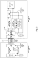
- Figure 1 is an illustration of an embodiment of a system for generating a stream clock from a data stream.
- a first device 100 includes a transmitter 110, the transmitter to transmit a data stream 140 via a communication link 145 according to a link clock rate 120, the data stream including content and other data 130 and timestamps 135 to indicate a relationship between the link clock signal 120 and a stream clock signal 125 for the transferred data.
- a second device 150 having a receiver 155 receives the data stream 140 via the communication link 145, the second device 150 operating to recover the link clock signal 160 and the timestamps 165 to regenerate the stream clock signal, the second device including a phase locked loop (PLL) 170 for use in generating the stream clock 175 and a buffer 180 to hold data 190 received from the data stream.
- the second device further provides for one or more measurements related to the data stream 185, the second device 150 operating to adjust the stream clock signal rate by modifying the rate of the phase locked loop 170 based at least in part on the one or more measurements 185.
- the one or more measurements 185 include a measurement of the number of pulses of the stream clock during a certain time period.
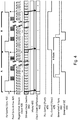
- FIG. 2 is a block diagram to illustrate an example of a system for regenerating a stream clock from a data stream.
- a source device 200 is coupled with a sink device 250 via an interface 240.
- the source device 200 may include a video controller 202 providing video data 204 to a transmitter (Txr) 206 for transmission via the interface 240 to the sink device 250.
- the video controller 202 operates according to a stream clock signal 212 and the transmitter 206 receives a link clock signal 214 for clocking of the data transmission via the interface 240.
- the stream clock signal 212 and the link clock signal 214 are further provided to an M/N counter 210, which utilizes such signals to generate M and N values 208 for transmission by the transmitter 206.
- the transmitted data stream thus includes the stream data and the M and N values 245.
- the sink device 250 further includes a receiver 252 to receive the data stream from the interface 250.
- the receiver 252 provides the received data to a clock and data recovery unit 254, which operates to recover data, directed to decoder 255, and to recover the link symbol clock signal 262, which is provided to a stream clock recovery unit 264 and to a buffer, shown as FIFO (first in, first out) buffer 266.
- Data recovered from the stream data is directed by the decoder 255 to a video data unpacker 256, which provides the video data to the FIFO buffer 266, and to an attribute unpacker 258, which obtains the M and N values 260 and provides such data to the stream data recovery unit 264.
- the sink device 250 may include a phase locked loop 265, which is illustrated as a part of the stream data recovery unit 264 but which may also be a separate element. Utilizing the link symbol clock signal and the M and N values the stream clock recovery unit 264 regenerates the stream clock signal, and provides the regenerated stream clock signal 268 to the FIFO buffer 266 and a video signal generator 270, which receives the video data from the FIFO buffer 266 based on the regenerated stream clock signal.
- a phase locked loop 265 which is illustrated as a part of the stream data recovery unit 264 but which may also be a separate element. Utilizing the link symbol clock signal and the M and N values the stream clock recovery unit 264 regenerates the stream clock signal, and provides the regenerated stream clock signal 268 to the FIFO buffer 266 and a video signal generator 270, which receives the video data from the FIFO buffer 266 based on the regenerated stream clock signal.
- the setting of the values of M and N varies based on the relationship of the clocks. If the two clock signals have the same clock source and are divided by a given number, then the source device is aware of the ratio of the two clock frequencies, and thus can set constant values for M and N. However, if the two clock signals have clock sources that are unrelated to each other, then the source device is required to calculate the M and N values over time, such as by counting the number of stream clock pulses during the time for a given number of link symbol clock pulses. As unrelated clock signals generally will drift in relation to each other, the values of M and N consequently change over time and must be recalculated over time. In a particular example, for DisplayPort in asynchronous mode, the N value is fixed as 32768.
- a sink device recovers the stream clock by extracting the time stamp values M and N from the received stream data and regenerating the stream clock.
- conventional operations to regenerate the stream clock in a sink device face certain difficulties.
- One difficulty is the complexity and size of the required PLL.
- the timestamp values M and N are 24-bit values, and a 24-bit fractional phase locked loop is generally required to generate an accurate stream clock signal.
- a 24-bit fractional PLL requires complex circuitry, and consequently requires a large amount of silicon area in a device or system.
- a higher resolution PLL that only addresses one of the M or N values at a time may be implemented in a sink device.
- the clock sources in the source device are imperfect due to frequency displacement.
- the M and N values themselves are not accurate because, for example, the values are updated once per 32,768 link symbol clock cycles, which requires hundreds of microseconds. If the phase differences are accumulated for such a time period, the phase differences may result in additional or missing clock pulses that can generate significant display artifacts and violations on the compliance with display devices. In order to compensate for inaccuracy, a very large FIFO buffer is required to prevent buffer underrun or overflow.
- the sink device operates to provide accurate regeneration of the stream clock utilizing measurements of the data stream.
- An apparatus or system may utilize a count of clock pulses between blank start or blank end symbols decoded by the attribute unpacker 258 in the determination of a stream clock signal.
- FIG 3 is a block diagram to illustrate a first embodiment of a system for regenerating a stream clock from a data stream including measurement of clock data pulses.
- a source device 300 transmits a data stream to a sink device 350.
- an apparatus, system, or method provides for counting the number of stream clock pulses between consecutive blank start symbols or blank end symbols (BS or BE).
- the video controller 202 of the source device 300 transfers to the sink device 350 a value of Htotal, where Htotal is a reference value representing the expected number of pulses in a period of a horizontal line.
- the operation by the illustrated attribute unpacker further includes detected blank start or blank end symbols and the Htotalvalue.
- the stream clock recovery unit 264 utilizes the M and N signals 260 together with the blank start or block end values and the Htotal value 361 in the regeneration of the stream clock signal 268. If the number of stream clock pulses generated between two blank start symbols or two blank end symbols is greater than Htotal, then the sink device 350 acts to slow the PLL 265 of the stream clock recovery unit 264, thereby reducing the rate of the regenerated stream clock signal. If the number of stream clock pulses generated for a certain time period, such as one horizontal line period, is less than Htotal, then the sink device 350 acts to increase the speed of the PLL 265 of the stream clock recovery unit 264, thereby increasing the rate of the regenerated stream clock signal.
- An apparatus, system, or method provides an opportunity to adjust the PLL more often than a conventional method based on timestamp M and N values only.
- the blank start and blank end signals are received for every line, while the time stamp value is generally updated once per several lines (such as every eight lines for a 1080p display).
- the required size of FIFO for preventing buffer underrun and overflow is much smaller than in a conventional method.
- an apparatus, system, or method allows for stream clock recovery to be handled earlier than in a conventional method, with a result that the clock phase error may be reduced, and the required FIFO size may be reduced because the overflow data is smaller in comparison with the conventional generation of the stream clock signal.
- FIG. 4 is a timing diagram to illustrate an embodiment of a process for regeneration of a stream clock signal.
- horizontal sync signals 410 are provided for lines of data, with pixel data being transmitted after the sync signals 420.
- a stream clock 430 is regenerated from a received data stream.
- An apparatus or system includes a stream clock counter 440 to determine the number of stream clock pulses in a period of time such as in any horizontal line, with the number being compared to an Htotal value 450, where the value is denoted as "H", the differences between and the count being shown as the clock count difference 460.
- an apparatus or system provides a PLL control signal (fast) 470 for causing the PLL to run faster, resulting in an increase in the stream clock rate, and a PLL control signal (slow) 475 for causing the PLL to run slower 475, resulting in a decrease in the stream clock rate.
- both the PLL control signal (fast) 470 and the PLL control signal (slow) 475 are disabled when the clock count difference is zero, with PLL (slow) 475 being enabled to decrease the stream clock rate when the clock count difference is a positive value.
- the PLL (fast) 470 would be enabled to increase the stream clock rate if the clock count difference becomes a negative value.
- Figure 4 further illustrates the generated horizontal sync signals 480 and the generated data 490.
- a method, apparatus, or system may use signal analysis including multiple measurements related to the received data stream.
- the regeneration of a clock signal includes both the determination of a number of clock pulses in a certain period and the determination of an amount of data stored in a buffer at a certain point in time.
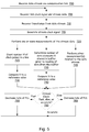
- Figure 5 is a flowchart to illustrate an embodiment of a process for regeneration of a clock signal.
- a process includes receiving a data stream at a receiving device from a transmitting device via a communication link 700, where the transmission of the data stream is clocked at a link clock signal rate.
- the process further includes recovering the link clock signal and stream data from the received data stream 705, and recovering time stamps providing a relationship between the link clock and a stream clock 710, the stream clock used for the transfer of data at the receiving device.
- the process further includes regenerating the link clock signal based at least in part on the link clock and the recovered timestamps 715.
- one or more measurements related to the data stream are made in order to adjust the frequency of the stream clock signal 720.
- the measurements related to the data stream include a count of a number H of clock pulses in a certain period of time such as in a line of data 725 and the comparison of the value H with a reference value 730.
- the measurements may include one or more other measurements related to the data stream 745.
- the process includes a determination based at least in part on the measurements related to the data stream whether the stream clock is running fast, is running slow, or is accurate 750. If the stream clock is running fast 750, then the process includes decreasing a rate of a phase locked loop element 755, thereby reducing the rate of the stream clock, and continuing with the process of recovering the link clock and stream data from the received data stream 705. If the stream clock is running slow 750, then the process includes increasing a rate of the phase locked loop 760, thereby increasing the rate of the stream clock, and continuing with the process of recovering the link clock and stream data from the received data stream. If the stream clock is running accurately 750, then the rate of a phase locked loop does not require adjustment, and continues with the process of recovering the link clock and stream data from the received data stream 705.
- the determination of whether the stream clock is accurate 750 includes a combination of the multiple measurements, whereby there is no need for adjustment of the PLL in conjunction with the adjustment of the stream clock, thereby reducing the rate of the stream clock, and continuing with the process of recovering the link clock and stream data from the received data stream.
- the present invention may include various processes.
- the processes of the present invention may be performed by hardware components or may be embodied in computer-readable instructions, which may be used to cause a general purpose or special purpose processor or logic circuits programmed with the instructions to perform the processes.
- the processes may be performed by a combination of hardware and software.
- Portions of the present invention may be provided as a computer program product, which may include a computer-readable storage medium having stored thereon computer program instructions, which may be used to program a computer (or other electronic devices) to perform a process according to the present invention.
- the computer-readable storage medium may include, but is not limited to, floppy diskettes, optical disks, CD-ROMs (compact disk read-only memory), and magneto-optical disks, ROMs (read-only memory), RAMs (random access memory), EPROMs (erasable programmable read-only memory), EEPROMs (electrically-erasable programmable read-only memory), magnet or optical cards, flash memory, or other type of media/ computer-readable medium suitable for storing electronic instructions.
- the present invention may also be downloaded as a computer program product, wherein the program may be transferred from a remote computer to a requesting computer.
- element A may be directly coupled to element B or be indirectly coupled through, for example, element C.
- a component, feature, structure, process, or characteristic A “causes” a component, feature, structure, process, or characteristic B, it means that "A” is at least a partial cause of "B” but that there may also be at least one other component, feature, structure, process, or characteristic that assists in causing "B.”
- a component, feature, structure, process, or characteristic may”, “might”, or “could” be included, that particular component, feature, structure, process, or characteristic is not required to be included. If the specification refers to "a” or “an” element, this does not mean there is only one of the described elements.
- An embodiment is an implementation or example of the invention.
- Reference in the specification to "an embodiment,” “one embodiment,” “some embodiments,” or “other embodiments” means that a particular feature, structure, or characteristic described in connection with the embodiments is included in at least some embodiments, but not necessarily all embodiments.
- the various appearances of "an embodiment,” “one embodiment,” or “some embodiments” are not necessarily all referring to the same embodiments. It should be appreciated that in the foregoing description of exemplary embodiments of the invention, various features of the invention are sometimes grouped together in a single embodiment, figure, or description thereof for the purpose of streamlining the disclosure and aiding in the understanding of one or more of the various inventive aspects.
Landscapes
- Engineering & Computer Science (AREA)
- Computer Networks & Wireless Communication (AREA)
- Signal Processing (AREA)
- Physics & Mathematics (AREA)
- Computer Hardware Design (AREA)
- General Physics & Mathematics (AREA)
- Theoretical Computer Science (AREA)
- Synchronisation In Digital Transmission Systems (AREA)
- Synchronizing For Television (AREA)
Applications Claiming Priority (3)
| Application Number | Priority Date | Filing Date | Title |
|---|---|---|---|
| US13/083,399 US8611486B2 (en) | 2011-04-08 | 2011-04-08 | Adjustment of clock signals regenerated from a data stream |
| PCT/US2012/030838 WO2012138515A2 (en) | 2011-04-08 | 2012-03-28 | Adjustment of clock signals regenerated from a data stream |
| EP12768459.5A EP2695323B1 (en) | 2011-04-08 | 2012-03-28 | Adjustment of clock signals regenerated from a data stream |
Related Parent Applications (2)
| Application Number | Title | Priority Date | Filing Date |
|---|---|---|---|
| EP12768459.5A Division EP2695323B1 (en) | 2011-04-08 | 2012-03-28 | Adjustment of clock signals regenerated from a data stream |
| EP12768459.5A Division-Into EP2695323B1 (en) | 2011-04-08 | 2012-03-28 | Adjustment of clock signals regenerated from a data stream |
Publications (2)
| Publication Number | Publication Date |
|---|---|
| EP3223431A1 EP3223431A1 (en) | 2017-09-27 |
| EP3223431B1 true EP3223431B1 (en) | 2018-07-25 |
Family
ID=46966131
Family Applications (2)
| Application Number | Title | Priority Date | Filing Date |
|---|---|---|---|
| EP17158908.8A Active EP3223431B1 (en) | 2011-04-08 | 2012-03-28 | Adjustment of clock signals regenerated from a data stream |
| EP12768459.5A Active EP2695323B1 (en) | 2011-04-08 | 2012-03-28 | Adjustment of clock signals regenerated from a data stream |
Family Applications After (1)
| Application Number | Title | Priority Date | Filing Date |
|---|---|---|---|
| EP12768459.5A Active EP2695323B1 (en) | 2011-04-08 | 2012-03-28 | Adjustment of clock signals regenerated from a data stream |
Country Status (7)
Families Citing this family (14)
| Publication number | Priority date | Publication date | Assignee | Title |
|---|---|---|---|---|
| US8989277B1 (en) | 2011-11-03 | 2015-03-24 | Xilinx, Inc. | Reducing artifacts within a video processing system |
| US9250646B2 (en) * | 2012-12-19 | 2016-02-02 | Intel Corporation | Clock recovery using remote arrival timestamps |
| US20160142343A1 (en) * | 2014-11-13 | 2016-05-19 | Broadcom Corporation | System for Recovery in Channel Bonding |
| KR101582171B1 (ko) * | 2014-11-19 | 2016-01-05 | 서울대학교산학협력단 | 직접 디지털 주파수 합성기를 이용한 디스플레이포트 수신단의 비디오 클럭 생성 구조 |
| CN110611543B (zh) * | 2018-06-14 | 2021-04-06 | 扬智科技股份有限公司 | 定时恢复的定时锁定识别方法与信号接收电路 |
| DE102018220301A1 (de) * | 2018-11-26 | 2020-05-28 | Festo Ag & Co. Kg | Kommunikationseinheit, Steuergerät, Kommunikationssystem und Verfahren |
| KR102655530B1 (ko) * | 2019-10-15 | 2024-04-08 | 주식회사 엘엑스세미콘 | 스트림 클럭 생성 장치 및 이를 포함하는 임베디드 디스플레이포트 시스템 |
| KR102518285B1 (ko) | 2021-04-05 | 2023-04-06 | 에스케이하이닉스 주식회사 | PCIe 인터페이스 및 인터페이스 시스템 |
| KR102519480B1 (ko) | 2021-04-01 | 2023-04-10 | 에스케이하이닉스 주식회사 | PCIe 장치 및 이를 포함하는 컴퓨팅 시스템 |
| US11546128B2 (en) | 2020-06-16 | 2023-01-03 | SK Hynix Inc. | Device and computing system including the device |
| KR102415309B1 (ko) * | 2020-06-16 | 2022-07-01 | 에스케이하이닉스 주식회사 | 인터페이스 장치 및 그 동작 방법 |
| CN115277983B (zh) * | 2022-06-22 | 2025-08-01 | 江苏珞珈聚芯集成电路设计有限公司 | 用于dp接口的视频像素时钟恢复方法与结构 |
| CN118250786A (zh) * | 2022-12-22 | 2024-06-25 | 华为技术有限公司 | 时钟同步方法、装置、芯片、芯片模组、系统及存储介质 |
| CN116580680B (zh) * | 2023-07-11 | 2024-02-20 | 苏州华星光电技术有限公司 | 显示面板的驱动方法、亮度补偿装置及显示装置 |
Family Cites Families (20)
| Publication number | Priority date | Publication date | Assignee | Title |
|---|---|---|---|---|
| JPH06303254A (ja) * | 1993-04-19 | 1994-10-28 | Matsushita Electric Ind Co Ltd | ソースクロック再生回路 |
| US5852630A (en) * | 1997-07-17 | 1998-12-22 | Globespan Semiconductor, Inc. | Method and apparatus for a RADSL transceiver warm start activation procedure with precoding |
| JP3540589B2 (ja) * | 1998-02-02 | 2004-07-07 | 株式会社東芝 | クロック逓倍回路 |
| JP2005079963A (ja) * | 2003-09-01 | 2005-03-24 | Pioneer Electronic Corp | 映像信号伝送システム及び方法並びに送信装置及び受信装置 |
| GB2409383B (en) * | 2003-12-17 | 2006-06-21 | Wolfson Ltd | Clock synchroniser |
| US7738617B1 (en) * | 2004-09-29 | 2010-06-15 | Pmc-Sierra, Inc. | Clock and data recovery locking technique for large frequency offsets |
| US7499462B2 (en) | 2005-03-15 | 2009-03-03 | Radiospire Networks, Inc. | System, method and apparatus for wireless delivery of content from a generalized content source to a generalized content sink |
| TW200731702A (en) * | 2005-07-29 | 2007-08-16 | Koninkl Philips Electronics Nv | Data stream synchronization |
| US7995143B2 (en) | 2006-02-10 | 2011-08-09 | Qualcomm Incorporated | Wireless video link synchronization |
| US7956856B2 (en) | 2007-02-15 | 2011-06-07 | Parade Technologies, Ltd. | Method and apparatus of generating or reconstructing display streams in video interface systems |
| US20090109988A1 (en) | 2007-10-26 | 2009-04-30 | Chowdhary Musunuri | Video Decoder with an Adjustable Video Clock |
| US8111799B2 (en) * | 2008-01-03 | 2012-02-07 | Dell Products L.P. | Method, system and apparatus for reducing power consumption at low to midrange resolution settings |
| US8391419B2 (en) * | 2008-03-17 | 2013-03-05 | Synaptics, Inc. | Circuit for recovering an output clock from a source clock |
| US8135105B2 (en) * | 2008-06-17 | 2012-03-13 | Integraded Device Technologies, Inc. | Circuit for correcting an output clock frequency in a receiving device |
| US20110235763A1 (en) * | 2009-01-12 | 2011-09-29 | Rambus Inc. | Signaling system with asymmetrically-managed timing calibration |
| EP3664323B1 (en) * | 2009-04-14 | 2021-07-07 | ATI Technologies ULC | Embedded clock recovery |
| JP5241638B2 (ja) * | 2009-07-23 | 2013-07-17 | 川崎マイクロエレクトロニクス株式会社 | 表示制御装置 |
| US8861669B2 (en) * | 2009-09-30 | 2014-10-14 | Synaptics Incorporated | Stream clock recovery in high definition multimedia digital system |
| US8217689B2 (en) * | 2010-01-19 | 2012-07-10 | Integrated Device Technology, Inc. | Method and circuit for DisplayPort video clock recovery |
| US20110193970A1 (en) * | 2010-02-11 | 2011-08-11 | Analogix Semiconductor, Inc. | Reducing Jitter in a Recovered Data Stream Clock of a Video DisplayPort Receiver |
-
2011
- 2011-04-08 US US13/083,399 patent/US8611486B2/en active Active
-
2012
- 2012-03-28 JP JP2014503686A patent/JP6040220B2/ja active Active
- 2012-03-28 CN CN201280016798.8A patent/CN103493424B/zh active Active
- 2012-03-28 EP EP17158908.8A patent/EP3223431B1/en active Active
- 2012-03-28 WO PCT/US2012/030838 patent/WO2012138515A2/en active Application Filing
- 2012-03-28 KR KR1020137029645A patent/KR101889373B1/ko active Active
- 2012-03-28 EP EP12768459.5A patent/EP2695323B1/en active Active
- 2012-04-02 TW TW101111755A patent/TWI536255B/zh active
Non-Patent Citations (1)
| Title |
|---|
| None * |
Also Published As
| Publication number | Publication date |
|---|---|
| TWI536255B (zh) | 2016-06-01 |
| WO2012138515A2 (en) | 2012-10-11 |
| CN103493424A (zh) | 2014-01-01 |
| WO2012138515A3 (en) | 2012-12-06 |
| KR101889373B1 (ko) | 2018-08-17 |
| JP6040220B2 (ja) | 2016-12-07 |
| EP3223431A1 (en) | 2017-09-27 |
| EP2695323A2 (en) | 2014-02-12 |
| EP2695323A4 (en) | 2014-08-27 |
| EP2695323B1 (en) | 2017-05-10 |
| CN103493424B (zh) | 2015-09-30 |
| KR20140048116A (ko) | 2014-04-23 |
| TW201301124A (zh) | 2013-01-01 |
| US8611486B2 (en) | 2013-12-17 |
| JP2014516489A (ja) | 2014-07-10 |
| US20120257699A1 (en) | 2012-10-11 |
Similar Documents
| Publication | Publication Date | Title |
|---|---|---|
| EP3223431B1 (en) | Adjustment of clock signals regenerated from a data stream | |
| CN101960770B (zh) | 时钟同步系统、节点和时钟同步方法 | |
| EP3526651B1 (en) | Precision time stamping method and system | |
| US7511762B2 (en) | Generation of a frame synchronized clock for a wireless video receiver | |
| EP2976866B1 (en) | Timestamp correction in a multi-lane communication link with skew | |
| EP2420013B1 (en) | Embedded clock recovery | |
| US5594763A (en) | Fast synchronizing digital phase-locked loop for recovering clock information from encoded data | |
| US20060020843A1 (en) | Technique to create link determinism | |
| US8913190B2 (en) | Method and apparatus for regenerating a pixel clock signal | |
| CN104461972B (zh) | 一种数据信号采样的方法和设备 | |
| US20140016654A1 (en) | Can communication system, can transmission apparatus, can reception apparatus, and can communication method | |
| US20070291856A1 (en) | Clock regeneration system and method for wireless media content delivery systems | |
| US9288418B2 (en) | Video signal transmitter apparatus and receiver apparatus using uncompressed transmission system of video signal | |
| KR101847366B1 (ko) | 시각 동기 장치 및 시각 동기 시스템 | |
| US8644378B2 (en) | Method and apparatus for de-spreading a spread-spectrum audio/video signal | |
| US7817765B2 (en) | Digital transmission apparatus and methods | |
| EP2664097A2 (en) | Mechanism for clock recovery for streaming content being communicated over a packetized communication network | |
| US8773291B2 (en) | Audio receiver and sample rate converter without PLL or clock recovery | |
| US20110193970A1 (en) | Reducing Jitter in a Recovered Data Stream Clock of a Video DisplayPort Receiver | |
| EP3731231B1 (en) | Slip detection on high speed data links | |
| CN103686215A (zh) | 分组发送接收装置和解扰系统 | |
| US7577221B2 (en) | Receiver scheme for synchronous digital transmission |
Legal Events
| Date | Code | Title | Description |
|---|---|---|---|
| PUAI | Public reference made under article 153(3) epc to a published international application that has entered the european phase |
Free format text: ORIGINAL CODE: 0009012 |
|
| STAA | Information on the status of an ep patent application or granted ep patent |
Free format text: STATUS: THE APPLICATION HAS BEEN PUBLISHED |
|
| AC | Divisional application: reference to earlier application |
Ref document number: 2695323 Country of ref document: EP Kind code of ref document: P |
|
| AK | Designated contracting states |
Kind code of ref document: A1 Designated state(s): AL AT BE BG CH CY CZ DE DK EE ES FI FR GB GR HR HU IE IS IT LI LT LU LV MC MK MT NL NO PL PT RO RS SE SI SK SM TR |
|
| STAA | Information on the status of an ep patent application or granted ep patent |
Free format text: STATUS: REQUEST FOR EXAMINATION WAS MADE |
|
| 17P | Request for examination filed |
Effective date: 20171006 |
|
| RBV | Designated contracting states (corrected) |
Designated state(s): AL AT BE BG CH CY CZ DE DK EE ES FI FR GB GR HR HU IE IS IT LI LT LU LV MC MK MT NL NO PL PT RO RS SE SI SK SM TR |
|
| GRAP | Despatch of communication of intention to grant a patent |
Free format text: ORIGINAL CODE: EPIDOSNIGR1 |
|
| STAA | Information on the status of an ep patent application or granted ep patent |
Free format text: STATUS: GRANT OF PATENT IS INTENDED |
|
| INTG | Intention to grant announced |
Effective date: 20180213 |
|
| GRAS | Grant fee paid |
Free format text: ORIGINAL CODE: EPIDOSNIGR3 |
|
| GRAA | (expected) grant |
Free format text: ORIGINAL CODE: 0009210 |
|
| STAA | Information on the status of an ep patent application or granted ep patent |
Free format text: STATUS: THE PATENT HAS BEEN GRANTED |
|
| AC | Divisional application: reference to earlier application |
Ref document number: 2695323 Country of ref document: EP Kind code of ref document: P |
|
| AK | Designated contracting states |
Kind code of ref document: B1 Designated state(s): AL AT BE BG CH CY CZ DE DK EE ES FI FR GB GR HR HU IE IS IT LI LT LU LV MC MK MT NL NO PL PT RO RS SE SI SK SM TR |
|
| REG | Reference to a national code |
Ref country code: GB Ref legal event code: FG4D |
|
| REG | Reference to a national code |
Ref country code: CH Ref legal event code: EP |
|
| REG | Reference to a national code |
Ref country code: AT Ref legal event code: REF Ref document number: 1022865 Country of ref document: AT Kind code of ref document: T Effective date: 20180815 |
|
| REG | Reference to a national code |
Ref country code: IE Ref legal event code: FG4D |
|
| REG | Reference to a national code |
Ref country code: DE Ref legal event code: R096 Ref document number: 602012049043 Country of ref document: DE |
|
| REG | Reference to a national code |
Ref country code: NL Ref legal event code: MP Effective date: 20180725 |
|
| REG | Reference to a national code |
Ref country code: LT Ref legal event code: MG4D |
|
| PG25 | Lapsed in a contracting state [announced via postgrant information from national office to epo] |
Ref country code: NL Free format text: LAPSE BECAUSE OF FAILURE TO SUBMIT A TRANSLATION OF THE DESCRIPTION OR TO PAY THE FEE WITHIN THE PRESCRIBED TIME-LIMIT Effective date: 20180725 |
|
| REG | Reference to a national code |
Ref country code: AT Ref legal event code: MK05 Ref document number: 1022865 Country of ref document: AT Kind code of ref document: T Effective date: 20180725 |
|
| PG25 | Lapsed in a contracting state [announced via postgrant information from national office to epo] |
Ref country code: IS Free format text: LAPSE BECAUSE OF FAILURE TO SUBMIT A TRANSLATION OF THE DESCRIPTION OR TO PAY THE FEE WITHIN THE PRESCRIBED TIME-LIMIT Effective date: 20181125 Ref country code: PL Free format text: LAPSE BECAUSE OF FAILURE TO SUBMIT A TRANSLATION OF THE DESCRIPTION OR TO PAY THE FEE WITHIN THE PRESCRIBED TIME-LIMIT Effective date: 20180725 Ref country code: AT Free format text: LAPSE BECAUSE OF FAILURE TO SUBMIT A TRANSLATION OF THE DESCRIPTION OR TO PAY THE FEE WITHIN THE PRESCRIBED TIME-LIMIT Effective date: 20180725 Ref country code: BG Free format text: LAPSE BECAUSE OF FAILURE TO SUBMIT A TRANSLATION OF THE DESCRIPTION OR TO PAY THE FEE WITHIN THE PRESCRIBED TIME-LIMIT Effective date: 20181025 Ref country code: SE Free format text: LAPSE BECAUSE OF FAILURE TO SUBMIT A TRANSLATION OF THE DESCRIPTION OR TO PAY THE FEE WITHIN THE PRESCRIBED TIME-LIMIT Effective date: 20180725 Ref country code: FI Free format text: LAPSE BECAUSE OF FAILURE TO SUBMIT A TRANSLATION OF THE DESCRIPTION OR TO PAY THE FEE WITHIN THE PRESCRIBED TIME-LIMIT Effective date: 20180725 Ref country code: NO Free format text: LAPSE BECAUSE OF FAILURE TO SUBMIT A TRANSLATION OF THE DESCRIPTION OR TO PAY THE FEE WITHIN THE PRESCRIBED TIME-LIMIT Effective date: 20181025 Ref country code: LT Free format text: LAPSE BECAUSE OF FAILURE TO SUBMIT A TRANSLATION OF THE DESCRIPTION OR TO PAY THE FEE WITHIN THE PRESCRIBED TIME-LIMIT Effective date: 20180725 Ref country code: RS Free format text: LAPSE BECAUSE OF FAILURE TO SUBMIT A TRANSLATION OF THE DESCRIPTION OR TO PAY THE FEE WITHIN THE PRESCRIBED TIME-LIMIT Effective date: 20180725 Ref country code: GR Free format text: LAPSE BECAUSE OF FAILURE TO SUBMIT A TRANSLATION OF THE DESCRIPTION OR TO PAY THE FEE WITHIN THE PRESCRIBED TIME-LIMIT Effective date: 20181026 |
|
| PG25 | Lapsed in a contracting state [announced via postgrant information from national office to epo] |
Ref country code: HR Free format text: LAPSE BECAUSE OF FAILURE TO SUBMIT A TRANSLATION OF THE DESCRIPTION OR TO PAY THE FEE WITHIN THE PRESCRIBED TIME-LIMIT Effective date: 20180725 Ref country code: LV Free format text: LAPSE BECAUSE OF FAILURE TO SUBMIT A TRANSLATION OF THE DESCRIPTION OR TO PAY THE FEE WITHIN THE PRESCRIBED TIME-LIMIT Effective date: 20180725 Ref country code: AL Free format text: LAPSE BECAUSE OF FAILURE TO SUBMIT A TRANSLATION OF THE DESCRIPTION OR TO PAY THE FEE WITHIN THE PRESCRIBED TIME-LIMIT Effective date: 20180725 |
|
| REG | Reference to a national code |
Ref country code: DE Ref legal event code: R097 Ref document number: 602012049043 Country of ref document: DE |
|
| PG25 | Lapsed in a contracting state [announced via postgrant information from national office to epo] |
Ref country code: EE Free format text: LAPSE BECAUSE OF FAILURE TO SUBMIT A TRANSLATION OF THE DESCRIPTION OR TO PAY THE FEE WITHIN THE PRESCRIBED TIME-LIMIT Effective date: 20180725 Ref country code: RO Free format text: LAPSE BECAUSE OF FAILURE TO SUBMIT A TRANSLATION OF THE DESCRIPTION OR TO PAY THE FEE WITHIN THE PRESCRIBED TIME-LIMIT Effective date: 20180725 Ref country code: IT Free format text: LAPSE BECAUSE OF FAILURE TO SUBMIT A TRANSLATION OF THE DESCRIPTION OR TO PAY THE FEE WITHIN THE PRESCRIBED TIME-LIMIT Effective date: 20180725 Ref country code: CZ Free format text: LAPSE BECAUSE OF FAILURE TO SUBMIT A TRANSLATION OF THE DESCRIPTION OR TO PAY THE FEE WITHIN THE PRESCRIBED TIME-LIMIT Effective date: 20180725 |
|
| PG25 | Lapsed in a contracting state [announced via postgrant information from national office to epo] |
Ref country code: SM Free format text: LAPSE BECAUSE OF FAILURE TO SUBMIT A TRANSLATION OF THE DESCRIPTION OR TO PAY THE FEE WITHIN THE PRESCRIBED TIME-LIMIT Effective date: 20180725 Ref country code: SK Free format text: LAPSE BECAUSE OF FAILURE TO SUBMIT A TRANSLATION OF THE DESCRIPTION OR TO PAY THE FEE WITHIN THE PRESCRIBED TIME-LIMIT Effective date: 20180725 Ref country code: DK Free format text: LAPSE BECAUSE OF FAILURE TO SUBMIT A TRANSLATION OF THE DESCRIPTION OR TO PAY THE FEE WITHIN THE PRESCRIBED TIME-LIMIT Effective date: 20180725 |
|
| PLBE | No opposition filed within time limit |
Free format text: ORIGINAL CODE: 0009261 |
|
| STAA | Information on the status of an ep patent application or granted ep patent |
Free format text: STATUS: NO OPPOSITION FILED WITHIN TIME LIMIT |
|
| 26N | No opposition filed |
Effective date: 20190426 |
|
| PG25 | Lapsed in a contracting state [announced via postgrant information from national office to epo] |
Ref country code: ES Free format text: LAPSE BECAUSE OF FAILURE TO SUBMIT A TRANSLATION OF THE DESCRIPTION OR TO PAY THE FEE WITHIN THE PRESCRIBED TIME-LIMIT Effective date: 20180725 |
|
| PG25 | Lapsed in a contracting state [announced via postgrant information from national office to epo] |
Ref country code: SI Free format text: LAPSE BECAUSE OF FAILURE TO SUBMIT A TRANSLATION OF THE DESCRIPTION OR TO PAY THE FEE WITHIN THE PRESCRIBED TIME-LIMIT Effective date: 20180725 |
|
| PG25 | Lapsed in a contracting state [announced via postgrant information from national office to epo] |
Ref country code: MC Free format text: LAPSE BECAUSE OF FAILURE TO SUBMIT A TRANSLATION OF THE DESCRIPTION OR TO PAY THE FEE WITHIN THE PRESCRIBED TIME-LIMIT Effective date: 20180725 |
|
| REG | Reference to a national code |
Ref country code: CH Ref legal event code: PL |
|
| PG25 | Lapsed in a contracting state [announced via postgrant information from national office to epo] |
Ref country code: LU Free format text: LAPSE BECAUSE OF NON-PAYMENT OF DUE FEES Effective date: 20190328 |
|
| REG | Reference to a national code |
Ref country code: BE Ref legal event code: MM Effective date: 20190331 |
|
| PG25 | Lapsed in a contracting state [announced via postgrant information from national office to epo] |
Ref country code: CH Free format text: LAPSE BECAUSE OF NON-PAYMENT OF DUE FEES Effective date: 20190331 Ref country code: IE Free format text: LAPSE BECAUSE OF NON-PAYMENT OF DUE FEES Effective date: 20190328 Ref country code: LI Free format text: LAPSE BECAUSE OF NON-PAYMENT OF DUE FEES Effective date: 20190331 |
|
| PG25 | Lapsed in a contracting state [announced via postgrant information from national office to epo] |
Ref country code: BE Free format text: LAPSE BECAUSE OF NON-PAYMENT OF DUE FEES Effective date: 20190331 |
|
| PG25 | Lapsed in a contracting state [announced via postgrant information from national office to epo] |
Ref country code: TR Free format text: LAPSE BECAUSE OF FAILURE TO SUBMIT A TRANSLATION OF THE DESCRIPTION OR TO PAY THE FEE WITHIN THE PRESCRIBED TIME-LIMIT Effective date: 20180725 |
|
| PG25 | Lapsed in a contracting state [announced via postgrant information from national office to epo] |
Ref country code: MT Free format text: LAPSE BECAUSE OF NON-PAYMENT OF DUE FEES Effective date: 20190328 Ref country code: PT Free format text: LAPSE BECAUSE OF FAILURE TO SUBMIT A TRANSLATION OF THE DESCRIPTION OR TO PAY THE FEE WITHIN THE PRESCRIBED TIME-LIMIT Effective date: 20181125 |
|
| PG25 | Lapsed in a contracting state [announced via postgrant information from national office to epo] |
Ref country code: CY Free format text: LAPSE BECAUSE OF FAILURE TO SUBMIT A TRANSLATION OF THE DESCRIPTION OR TO PAY THE FEE WITHIN THE PRESCRIBED TIME-LIMIT Effective date: 20180725 |
|
| PG25 | Lapsed in a contracting state [announced via postgrant information from national office to epo] |
Ref country code: HU Free format text: LAPSE BECAUSE OF FAILURE TO SUBMIT A TRANSLATION OF THE DESCRIPTION OR TO PAY THE FEE WITHIN THE PRESCRIBED TIME-LIMIT; INVALID AB INITIO Effective date: 20120328 |
|
| PG25 | Lapsed in a contracting state [announced via postgrant information from national office to epo] |
Ref country code: MK Free format text: LAPSE BECAUSE OF FAILURE TO SUBMIT A TRANSLATION OF THE DESCRIPTION OR TO PAY THE FEE WITHIN THE PRESCRIBED TIME-LIMIT Effective date: 20180725 |
|
| P01 | Opt-out of the competence of the unified patent court (upc) registered |
Effective date: 20230929 |
|
| PGFP | Annual fee paid to national office [announced via postgrant information from national office to epo] |
Ref country code: DE Payment date: 20250327 Year of fee payment: 14 |
|
| PGFP | Annual fee paid to national office [announced via postgrant information from national office to epo] |
Ref country code: FR Payment date: 20250325 Year of fee payment: 14 |
|
| PGFP | Annual fee paid to national office [announced via postgrant information from national office to epo] |
Ref country code: GB Payment date: 20250327 Year of fee payment: 14 |