EP3221985B1 - Verfahren und vorrichtung, zur steuerung, überwachung und kommunikation mit abstimmbaren optischen vorrichtungen und baugruppen - Google Patents
Verfahren und vorrichtung, zur steuerung, überwachung und kommunikation mit abstimmbaren optischen vorrichtungen und baugruppen Download PDFInfo
- Publication number
- EP3221985B1 EP3221985B1 EP15807748.7A EP15807748A EP3221985B1 EP 3221985 B1 EP3221985 B1 EP 3221985B1 EP 15807748 A EP15807748 A EP 15807748A EP 3221985 B1 EP3221985 B1 EP 3221985B1
- Authority
- EP
- European Patent Office
- Prior art keywords
- control
- field programmable
- laser
- programmable device
- optical
- Prior art date
- Legal status (The legal status is an assumption and is not a legal conclusion. Google has not performed a legal analysis and makes no representation as to the accuracy of the status listed.)
- Active
Links
Images







Classifications
-
- H—ELECTRICITY
- H04—ELECTRIC COMMUNICATION TECHNIQUE
- H04B—TRANSMISSION
- H04B10/00—Transmission systems employing electromagnetic waves other than radio-waves, e.g. infrared, visible or ultraviolet light, or employing corpuscular radiation, e.g. quantum communication
- H04B10/50—Transmitters
- H04B10/501—Structural aspects
- H04B10/503—Laser transmitters
- H04B10/505—Laser transmitters using external modulation
- H04B10/5057—Laser transmitters using external modulation using a feedback signal generated by analysing the optical output
-
- H—ELECTRICITY
- H04—ELECTRIC COMMUNICATION TECHNIQUE
- H04B—TRANSMISSION
- H04B10/00—Transmission systems employing electromagnetic waves other than radio-waves, e.g. infrared, visible or ultraviolet light, or employing corpuscular radiation, e.g. quantum communication
- H04B10/50—Transmitters
- H04B10/501—Structural aspects
- H04B10/503—Laser transmitters
-
- H—ELECTRICITY
- H01—ELECTRIC ELEMENTS
- H01S—DEVICES USING THE PROCESS OF LIGHT AMPLIFICATION BY STIMULATED EMISSION OF RADIATION [LASER] TO AMPLIFY OR GENERATE LIGHT; DEVICES USING STIMULATED EMISSION OF ELECTROMAGNETIC RADIATION IN WAVE RANGES OTHER THAN OPTICAL
- H01S5/00—Semiconductor lasers
- H01S5/06—Arrangements for controlling the laser output parameters, e.g. by operating on the active medium
- H01S5/068—Stabilisation of laser output parameters
- H01S5/0683—Stabilisation of laser output parameters by monitoring the optical output parameters
- H01S5/0687—Stabilising the frequency of the laser
-
- H—ELECTRICITY
- H04—ELECTRIC COMMUNICATION TECHNIQUE
- H04B—TRANSMISSION
- H04B10/00—Transmission systems employing electromagnetic waves other than radio-waves, e.g. infrared, visible or ultraviolet light, or employing corpuscular radiation, e.g. quantum communication
- H04B10/50—Transmitters
- H04B10/572—Wavelength control
-
- H—ELECTRICITY
- H01—ELECTRIC ELEMENTS
- H01S—DEVICES USING THE PROCESS OF LIGHT AMPLIFICATION BY STIMULATED EMISSION OF RADIATION [LASER] TO AMPLIFY OR GENERATE LIGHT; DEVICES USING STIMULATED EMISSION OF ELECTROMAGNETIC RADIATION IN WAVE RANGES OTHER THAN OPTICAL
- H01S5/00—Semiconductor lasers
- H01S5/005—Optical components external to the laser cavity, specially adapted therefor, e.g. for homogenisation or merging of the beams or for manipulating laser pulses, e.g. pulse shaping
-
- H—ELECTRICITY
- H01—ELECTRIC ELEMENTS
- H01S—DEVICES USING THE PROCESS OF LIGHT AMPLIFICATION BY STIMULATED EMISSION OF RADIATION [LASER] TO AMPLIFY OR GENERATE LIGHT; DEVICES USING STIMULATED EMISSION OF ELECTROMAGNETIC RADIATION IN WAVE RANGES OTHER THAN OPTICAL
- H01S5/00—Semiconductor lasers
- H01S5/005—Optical components external to the laser cavity, specially adapted therefor, e.g. for homogenisation or merging of the beams or for manipulating laser pulses, e.g. pulse shaping
- H01S5/0085—Optical components external to the laser cavity, specially adapted therefor, e.g. for homogenisation or merging of the beams or for manipulating laser pulses, e.g. pulse shaping for modulating the output, i.e. the laser beam is modulated outside the laser cavity
Definitions
- transceivers as the interface between electronics and optical signals that propagate on the optical fiber and at other points in the network where information is converted between electronic form and optical form.
- Optical devices including optical, photonic and optoelectronic devices and components are used to transmit, code, receive, and decode optical data for transmission on an optical fiber.
- the optical devices are interfaced to a variety of electronic circuits which are used to control the devices and components, as well as interface data in electronic form on the transmit and receive side, code and decode electronic data, perform other functions like clock recovery and error correction and realize functions required to control an environment of the circuitry including temperature, wavelength and other tunable laser functions and functions of the interface optics and circuits that are used to realize a fully operational tunable laser and tunable subassembly.
- Programmable optical devices such as transmitters, optical subassemblies, and transceivers, based on a tunable laser, require many control systems to support the functions of the tunable laser and support the control, monitoring and communications functionality.
- a widely tunable laser includes multiple sections, generally including a gain section, a tunable phase section, and tunable mirror sections and in some designs a tunable filter section is also incorporated. Tuning the physical parameters of these sections results in tuning of an output laser wavelength.
- Other parameters of the tunable laser include an optical data modulator, if it is integrated or not integrated, and other functions like power control, wavelength locking, linewidth narrowing and control, modulation control, higher order modulation, or the like, performance of which may be enhanced using the present disclosure.
- Known prior art programmable wavelength tunable transmitters such as transmitter optical subsystem assembly (TOSA), transceivers and other communications optical subassemblies, however, are not programmable in real-time and thus lack flexibility and responsiveness at the optical layer. Further, as the existing devices lack real time programmability, there is a high cost associated with planning, building, operating and maintaining data center networks.
- TOSA transmitter optical subsystem assembly
- transceivers and other communications optical subassemblies
- the present disclosure relates generally to optical devices and subassemblies, such as optical transceivers, modules and subassemblies as well as laser transmitters and receivers that employ integrated electronics and photonic integrated circuits and combinations thereof.
- the optical devices and subassemblies contain multiple elements, for example, widely tunable semiconductor lasers integrated on the same substrate with optical modulators and semiconductor optical amplifiers, non-integrated optical and optoelectronic elements, and other measurement and control devices and elements.
- an apparatus for controlling, monitoring, and communicating with an optical device, photonic integrated circuit or subassembly for optical communications includes an optical device or subassembly and a field programmable device including programmable hardware gates coupled to the optical device or subassembly.
- the field programmable device is configured to implement a plurality of functions at a gate level for controlling, monitoring, and/or communicating with the optical device or subassembly, each of the plurality of functions being configured to execute as a concurrent process within the field programmable device; the plurality of functions including functions to obtain one or more gain-voltage maps by tuning laser mirror currents of the tunable laser at a temperature value; and the plurality of functions further including functions to determine lasing wavelengths corresponding to minima of the one or more gain-voltage maps according to a temperature, the lasing wavelengths being used for tuning or calibrating the tunable laser of the optical device.
- an optical communication system includes an optical device or subassembly comprising a tunable laser integrated on a same substrate with an optical modulator and a semiconductor optical amplifier, non-integrated optical and optoelectronic elements; and a field programmable device including programmable hardware gates coupled to the optical device or subassembly and the laser transmitter and receiver.
- the field programmable device is configured to implement a plurality of functions at a gate level for controlling, monitoring, and/or communicating with the optical device or subassembly, each of the plurality of functions being configured to run as a concurrent process, without use of a microprocessor or a microcontroller.
- the field programmable device of the optical communication system comprises one or more field programmable gate arrays (FPGAs) or programmable logic devices (PLDs). Further, the field programmable device of the optical communication system may be configured to comprise application programmable interfaces (APIs) for real-time control and monitoring of the optical device and subassembly based on actual traffic flows. Also, the plurality of functions may be configured to run at different clock signals in the field programmable device.
- FPGAs field programmable gate arrays
- PLDs programmable logic devices
- APIs application programmable interfaces
- the plurality of functions may be configured to run at different clock signals in the field programmable device.
- the field programmable device may comprise a communication interface including one or both of sockets to a graphical user interface (GUI) or an application programming interface (API) that allows control, monitoring and/or communication with the tunable laser integrated on the same substrate with the optical modulator and the semiconductor optical amplifier, non-integrated optical and optoelectronic elements.
- GUI graphical user interface
- API application programming interface
- the present disclosure comprises real-time programmable optical devices and subassemblies, such as wavelength tunable transmitters (e.g., TOSA), transceivers, and other communications optical subassemblies.
- software-enabled features accessible via application programmable interfaces (APIs), offer extensive real-time control and monitoring of the optical devices and subassemblies based on, for example, actual traffic flows.
- APIs application programmable interfaces
- Programmability enables an unprecedented level of flexibility and responsiveness at the optical layer with real-time scaling and rerouting of bandwidth, higher bandwidth extraction from a given fiber plant as well as a reduction in complexity and related cost of planning, building, operating and maintaining data center networks.
- programmable systems, methods and devices are provided to control, monitor and communicate with tunable lasers, tunable transmitters, tunable transceiver pluggables and subassemblies, and board mounted tunable transceivers and the auxiliary integrated or non-integrated optics, optoelectronics and/or electronics.
- the systems, methods and devices described herein realize functions to design, build, produce and manufacture a fully functional tunable laser, tunable transmitter, tunable transceiver, pluggable, subassembly or board mount.
- the present disclosure implements monitoring and control and communications functions for the tunable laser, transceiver, module or optical subassembly in a field programmable device including a field programmable gate array (FPGA) or programmable logic device (PLD) circuitry architecture, or in combination with a microprocessor or microcontroller.
- FPGA field programmable gate array
- PLD programmable logic device
- Both the FPGA and PLD circuitry are reconfigurable circuitry, which can be programmed/re-programmed in the field and/or real-time after manufacture.
- the control functions of the optical device or subassembly can be implemented without a microcontroller or microprocessor.
- various functions including control functions may be embedded in the FPGA or PLD.
- the functions that are embedded in the FPGA or PLD include, but are not limited to, soft state machines, electronic filters, control and feedback loops, decisions circuits, communications interfaces, etc., which are implemented by embedding concurrent processes in the FPGA, the PLD or the combination of programmable logic and microprocessor.
- the present disclosure is an advance over existing technologies that utilize microprocessors or microcontrollers for control and programmable logic devices such as FPGAs or PLDs to store calibration and other data for lookup operation(s).
- control, monitoring and communications functions to build and operate a tunable transmitter, tunable laser, tunable transceiver, pluggable or subassembly may be programmed in hardware gates in the FPGA, using firmware, each running at their own clock speed and implemented modularly.
- firmware each running at their own clock speed and implemented modularly.
- the concurrency, modularity, ability to run processes at different clock speeds, may result in advances over the existing technology for reduced costs, complexity, power consumption, and other advantages.
- the present disclosure includes, but is not limited to, the control, monitor and communications method and apparatus for a tunable laser/transceiver which is programmable and firmware updatable, and may be fully FPGA controlled (no microprocessor or microcontroller required).
- Embodiments of the present disclosure may include, but are not limited to:
- control systems and methods are provided to rapidly control an optical device and/or subassembly.
- the control systems and methods comprise functionality to control elements of the optical device or subassembly, such as a tunable laser, internal and external optical and optoelectronic monitoring and control functions, internal and external electronic monitoring and control functions, signal processing functions, and associated functions in a transceiver, optical module and/or optical subassembly.
- a field programmable device such as a FPGA, PLD, or the like, either stand alone or in combination with a microcontroller, and/or in combination with analog to digital converting (ADC) and digital to analog converting (DAC) circuits, where the FPGA, PLD, or the like is used for the control functions as part of the first embodiment, beyond the simple present day use of FPGAs and PLDs as data storage only mechanisms, for example, lookup tables for tunable lasers.
- ADC analog to digital converting
- DAC digital to analog converting
- This embodiment of the present disclosure thus provides various advantageous over the existing technology, which utilizes FPGAs and/or PLDs in a limited capacity to store data about tunable lasers and other embodiments to be accessed by other processing modules for monitoring, control and processing, but not for the control systems and methods as described herein.
- the field programmable device may be configured to automatically adapt laser control currents of a tunable laser to measured temperature so as to reduce a load on a thermoelectric cooler (TEC), based on the measured temperature and at least one of: by moving between tables stored in the field programmable device or by extrapolating between temperature wavelength maps.
- TEC thermoelectric cooler
- An advantage of using the field programmable device, such as the FPGA, PLD, or the like, as part of the control systems and methods according to the present disclosure is that code and processes may be modular and/or concurrent processes, each may run at different, unique clocks speeds within the same device and is reprogrammable, and can handle all control, monitoring, and communication embodiments. Accordingly, in an aspect of the present disclosure, one or more submodules of the system can be replaced, modified, programmed, and/or re-programmed without affecting other modules/submodules.
- advantages of running the control, monitoring, and communications systems of the optical devices and subassemblies in a programmable manner at a gate level may include lower power consumption, lower cost, wider use across broader classes of applications, and introduction of new control modules of a variety of types (filter, analog circuits, state machines, etc.) in a common programmable architecture.
- the methods and systems described herein may be utilized with a multi-facet laser architecture, as described in U.S. Patent Application Ser. No. 14/146717, published on July 10, 2014 as WO2014/107537 .
- two or more facet of a tunable laser may be used for an output and may be connected to a novel modulator structure.
- the control and monitoring described in the present disclosure in certain forms, may have additional advantages over prior state of the art when combined with the inventions described in WO2014/107537 .
- the present disclosure may be employed with optical devices and subassemblies that use an FPGA centric architecture.
- devices and subassemblies may include U.S. Patent No. 8,644,713 , and U.S. Patent Application Ser. Nos. 14/171,480 , titled “Programmable Optical Subassemblies and Modules”; 12/945,470 , titled “Optical Network Interface Module Using A Hardware Programmable Optical Network”; and 13/942,519, titled “Control Systems for Optical Devices and Subassemblies,".
- the FPGA centric architecture may run all control, monitoring, communications, algorithms using an internal FPGA without use of a microprocessor or microcontroller in these optical devices and subassemblies.
- the same firmware for an external FPGA may also be used to calibrate the laser and significantly speed up the calibration speed, where the resulting calibration data is then ported to a wavelength control FPGA which is used to control the tunable laser, making the calibration during manufacturing and the control and re-calibration or re-programming uniform with FPGA technology and firmware across all embodiments of the use of a tunable laser from manufacturing to deployment in a network.
- the present technology may significantly cut down on the cost of manufacturing and ownership as well as improving performance.
- a communications interface may be integrated into the field programmable device (e.g., FPGA) as described in U.S. Patent Application Ser. No. 12/945, 470 .
- the communications interface may comprise sockets to graphical users interfaces (GUIs) and/or application programmable interfaces (API) that allow software control, monitoring and calibration of a complete tunable laser using a software layer that interacts with the tunable laser through the field programmable device (e.g. FPGA or PLD or the like) to implement one of any of the fast wavelength calibration algorithms, making the ease of use, manufacturability, speed of calibration, and integration into other manufacturing, system integration and network operation systems enabled and significantly lower cost and flexible compared to any existing approach.
- the speed of the calibration routines on the order of minutes, may even allow recalibration in the field or real-time using the application layer interfaces via the field programmable device (e.g., FPGA, PLD or the like).
- the field programmable device may be configured to receive one or more control signals from a GUI coupled to the field programmable device via wireless communications or from a GUI of another apparatus located at a remote site over an optical communication link.
- Other significant advantages of the present disclosure may also include the ability to utilize processes embedded in the field programmable device (e.g., FPGA, PLD or the like), in addition to control and monitoring interfaces, to realize all functions needed to improve the performance of the tunable laser and transmitter using firmware, for example, narrowing a laser linewidth for coherent communications, reducing the laser relative intensity noise (RIN), as two of many examples.
- These processes may be run in parallel with all other processes for the tunable laser, transmitter, transceiver, module or subassembly, and in many cases can re-use hardware used for other functions.
- optical devices such as optical transmitters, optical subassemblies, and transceivers which are programmable are described.
- the programmable optical devices are based on a tunable laser having field programmable device centric (e.g., a FPGA or a PLD centric) control systems which support various functions of the tunable laser and supporting control, monitoring and communications functionality.
- the present disclosure comprises real-time programmable wavelength tunable transmitters, such as transmitter optical subassemblies (TOSAs), transceivers, and other communications optical subassemblies.
- TOSAs transmitter optical subassemblies
- transceivers and other communications optical subassemblies.
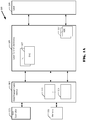
- FIG. 1A illustrates a block diagram conceptually showing components for a field programmable device centric (e.g., FPGA/PLD centric) control system.
- a system 100 shown in FIG. 1 includes a host controller 101, a field programmable device 103 (e.g., FPGA, PLD or the like), laser control electronics 105, a tunable laser 109, and a storage 111.
- the host controller 101 may be configured to communicate with the field programmable device 103 for various functions, and also configured to receive data relating to operation of the tunable laser 109.
- the field programmable device 103 may drive the laser control electrodes 105 through digital-to-analog converters (DACs) 107 interfaced to the field programmable device 103 and the tunable laser 109. Further, the field programmable device 103 may be coupled to the tunable laser 109 through analog-to-digital converters (ADCs) 117 for communications and control of the tunable laser 109.
- DACs digital-to-analog converters
- ADCs analog-to-digital converters
- the field programmable device 103 may also include various components, modules or processes (which are not shown in FIG. 1A , but described herein in detail), such as communication interfaces to/from a client or host for fiber communications channel; tunable laser wavelength memory and management; PROM-SPI Flash interface to external memory; setting currents and voltages for all control and monitoring functions for the tunable laser, modulator, optoelectronics, sensor and other control and monitor points that interface via voltages and currents; optical and electronic and photonic integrated circuit (PIC) monitors; boxcar averagers and signal processing functions; automatic optical power control; wavelength locking; linewidth narrowing functions, temperature monitoring and control; alarm and monitoring control and communications; application programming interfaces (APIs); and many other functions for implementing various aspects of the present methodology described herein.
- various components, modules or processes which are not shown in FIG. 1A , but described herein in detail, such as communication interfaces to/from a client or host for fiber communications channel; tunable laser wavelength memory and management; PROM-
- the field programmable device 103 may include an internal storage (not shown) and/or an external storage such as the storage or memory 111 coupled to the field programmable device 103 for storing various parameters including parameters for implementing various aspects of the present technology.
- the memory 111 may include one or more look-up tables of data in connection with implementing various aspects of the present technology described herein.
- a field programmable device-centric architecture may be implemented as follows.
- the host controller 101 may transfer code for one or more algorithms, modules, processes or functions to the field programmable device 103, either as high level programming language (e.g., C code or the like) in an embedded soft processor, or for even more efficiency and high speed, as hardware description language (e.g., HDL code or the like).
- the host computer 101 may also be connected through a standard interface, i.e., a universal serial bus (USB) connection, to the field programmable device 103.
- USB universal serial bus
- the field programmable device 103 may communicate directly with DACs 117 that are configured to drive currents to various components including laser mirrors of the tunable laser 109 and communicates with ADCs 107 that are configured to monitor the electrode voltages and/or power detectors to collect data from the tunable laser 109 in accordance with various aspects of the present technology.
- the field programmable device 103 may control transients in laser temperature by monitoring a thermistor on the tunable laser 109 and driving a current control input to a TEC controller of the tunable laser 109.
- the field programmable device 103 may buffer or store data relating to controlling, monitoring, and communicating with the tunable laser 109 in one or more storage devices, such as the memory 111, whether it is internal or external to the field programmable device 103, to perform various functions, methods, algorithms or methodologies, in accordance with aspects of the present disclosure.
- the present technology may be viewed as a field programmable device (e.g., FPGA, PLD or the like) centric architecture for optical communications systems.
- the one or more implementations of the present technology may be optimized for a hardware architecture and the methodology or algorithm itself, incurring negligible overhead in the processing of various aspects of the present technology in the field programmable device 103, and thus data transfers to and from the coupled ADCs 107, DACs 117, and storage 111 may be very efficient.
- the present disclosure provides software-enabled features accessible via application programmable interfaces (APIs), offering extensive real-time control and monitoring of one or more modules or processes based on, for example, actual traffic flows.
- APIs application programmable interfaces
- Such programmability provides an unprecedented level of flexibility and responsiveness at an optical layer with real-time scaling and rerouting of a bandwidth, a higher bandwidth extraction from a given fiber plant as well as a reduction in complexity and related cost of planning, building, operating and maintaining data center networks.
- Rapid control of all aspects of a tunable laser, in which more than one facet are optically available, or integrated transmitter photonic integrated circuit (PIC) assembly that combines a tunable laser and modulator, or optical transceiver or optical subassembly is provided.
- control which is modular, concurrent, independent processes, fast and reprogrammable, and thus may handle all control, monitoring, and communication aspects, in which any sub-module of a system may be replaced, modified, programmed without affecting other modules or processes.
- control, monitoring, and communications system may comprises modular, independent, and/or concurrent processes configured to run in the field programmable device, each of which may be configured to run at different clocks.
- the present disclosure may provide for control, monitoring, communications, and algorithm implementations using an internal field programmable device such as am FPGA, PLD, or the like, without using a microprocessor or a microcontroller, and may even use the same firmware for an external FPGA, which is used to calibrate a tunable laser, thereby significantly speeding up the calibration speed of the tunable laser.
- an internal field programmable device such as am FPGA, PLD, or the like
- the resulting calibration data may then be ported to a wavelength control FPGA which is used to control the tunable laser, making the calibration during manufacturing and the control and re-calibration or re-programming uniform with the field programmable device based technology described herein and firmware across all aspects of the use of a tunable laser from manufacturing to deployment in a network, significantly cutting down on the cost of manufacturing and ownership as well as improving performance.
- the communications interface into the field programmable device 103 may provide gate level general programming and interfaces for graphical users interfaces (GUIs) and/or application programmable interfaces (API) that allow software control, monitoring and calibration of a complete tunable laser using a software layer that interacts with the tunable laser through the field programmable device 103 to implement one of any of the algorithms described herein including the fast wavelength calibration algorithms, making the ease of use, manufacturability, speed of calibration, and integration into other manufacturing, system integration and network operation systems enabled and significantly lower cost and make flexible compared to any prior existing technology.
- the speed of the calibration routines, on the order of minutes, may even allow recalibration in the field or real-time using the application layer interfaces via the field programmable device (e.g., FPGA, PLD or the like).
- Advantages of the present disclosure may include, but not limited to, many significant advantages over the existing technology that uses a microcontroller or microprocessor as a main control and an FPGA primarily as a data storage and lookup device.
- the performance as a function of footprint and power consumption of field programmable devices such as FGPAs was not considered competitive to microprocessors to handle various functions required for real time data and control in tunable laser applications.
- field programmable device technology including FPGA, PLD, or the like technology, has advanced significantly and has become a preferred and more flexible method and apparatus to control, monitor and communicate than many microcontroller or microprocessor based solutions.
- a field programmable device such as an FPGA is an integrated circuit that can be programmed in the field or real-time after manufacture, unlike certain integrated circuits such as a microcontroller or a microprocessor, which is hard-core. That is, FPGAs are semiconductor device that are based on a programmable/configurable logic blocs connected via programmable interconnects or wiring circuits, thereby enabling the FPGAs to be reprogrammable to desired application or functionality requirements after manufacturing. In other words, an FPGA is a device based on a gate and device interconnection loaded into the FPGA to operate on data and signals at inputs to generate outputs.
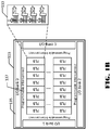
- the field programmable device 103 may include an FPGA or PLD or the like comprising a plurality of configurable logic blocks (CLBs) 133, a plurality of input /output (I/O) ports 135, programmable interconnect 137, etc.
- CLB configurable logic block
- Each configurable logic block 133 (CLB) may include various components, such as carry logic, input look-up tables, flip-flops, etc.
- the operation of the FPGA as well as the clock speed of different processes running on the FPGA may be changed in real time, and thus a wide variety of control, monitoring, feedback, communications and other functions may be realized with hardware level performance in the FPGA.
- a field programmable device e.g., FPGA, PLD, or the like
- FPGA field programmable device
- PLD PLD
- different areas of the FPGA circuitry may be allocated or used to implement different data and/or control functions all within the single device.
- a plurality of data and/or control functions or modules may be implemented in one or more PLBs, e.g., a wavelength locking 151, wavelength mapping and lookup 153, TEC control 155, automatic power control (APC) 157, PHD Linewidth control 159, communications I/O 161, etc., each running at different clock signals, e.g., clock 1, 2, ... 6.
- PLBs e.g., a wavelength locking 151, wavelength mapping and lookup 153, TEC control 155, automatic power control (APC) 157, PHD Linewidth control 159, communications I/O 161, etc.
- APC automatic power control
- PHD Linewidth control 159 PHD Linewidth control 159
- communications I/O 161, etc. each running at different clock signals, e.g., clock 1, 2, ... 6.
- a new module or process such as a P
- programmable firmware functions may include but not limited to (functions or examples below may be implemented alone or in combination with others):
- FIG. 1C illustrates an example of how some of the functions that may be implemented as concurrent, modular processes, while providing an advantage over the existing technology using a microcontroller and/or a serial state machine as shown in FIG. 2 , which illustrates a typical implementation of a tunable laser or transceiver control, monitor, and communications using a microprocessor or microcontroller based architecture.
- the microprocessor or microcontroller by design executes the functions, modules or processes in a sequential manner, for example, executing the wavelength mapping and lookup 161, wavelength locking 163, APC 165, TEC control 167, and communication I/O 168. Further, if a new function such as a PDH LW control 173 is to be added (at 171), then code need to be redesigned for the microprocessor or microcontroller.
- the present technology provides the field programmable device 103 (e.g., FPGA, PLD or the like) which may implement various functions, modules or processes relating to control, monitor, and communication with a tunable laser or transceiver, as concurrent, independent modules or processes which are configured to run at different clock signals, without use of the microprocessor or microcontroller.
- FPGA field programmable device
- the field programmable device 103 may include a slave controller that may implement standard serial protocols, such as an Inter-IC bus (I2C) and/or serial peripheral interface (SPI), or other proprietary protocols.
- standard serial protocols such as an Inter-IC bus (I2C) and/or serial peripheral interface (SPI), or other proprietary protocols.
- I2C Inter-IC bus
- SPI serial peripheral interface
- SoC system-on-chip
- a register map architecture may be based on two dual port random access memories (RAMs), one for a register map and one for wavelength table data which may be implemented in (or external but coupled to) the field programmable device 103. Host read/writes to the register map may then be directly addressed to one port of the register table RAM, while up/download of the wavelength table data is accomplished through a set of registers that include the parameters for a single wave table entry and redirect this data to an appropriate location in a wave table RAM.
- RAMs dual port random access memories
- the second RAM port may be used for updating of digital-to-analog (DAC) data from RAM, reading of analog-to-digital (ADC) monitor data to RAM, and updating of laser/modulator control parameters from the wave table RAM when wavelength is changed or as dictated by a system.
- DAC digital-to-analog
- ADC analog-to-digital
- Dedicated control logic may perform RAM to ADC/DAC transactions, without the use of a microcontroller or microprocessor.
- the logic implemented in the field programmable device 103 may be optimized further for transfer efficiency, has predictable latency, and can be tuned to prioritize transactions that require very low latency.
- a registered memory map of the field programmable device 103 may be implemented within the field programmable device 103 and controlled via a host communication interface.
- the registered memory map may define a current state of a control system, which in turn determines the wavelength and output power of a tunable laser assembly.
- the state of a control system may be a result of electrode currents, bias voltages, device operating temperature and various configurable settings associated with the tunable laser like a TEC PID control loop and wavelength locker, for example. All of these individually configurable modules or processes may be changed and monitored by writing to or reading from an appropriate register in the registered memory map of the field programmable device 103, without the use of the microprocessor or microcontroller.
- FIG. 3 an example implementation of a Register Write operation via UART is shown in FIG. 3 .
- a UART is used to communicate to an I2C device.
- the field programmable device 103 receives a command from a host or host controller 101 via a UART string (e.g., UART Tx from the host to the field programmable device), the UART string is echoed back to the host or host controller (e.g., UART Rx from the field programmable device to the host), the command is then interpreted, and an I2C command is issued to a register interface on the I2C bus coupled to the field programmable device 103.
- the UART then sends a string back with the written data.
- for a register write cycle it may take approximately 1.2 ms.
- API Automatic Power Control
- an automatic power control (APC) function or loop may be implemented as a concurrent, independent module or process within the field programmable device 103.
- An APC control function or loop dynamically maintains a laser output power at a commanded level while also maintaining a ratio of semiconductor optical amplifier (SOA) currents in a tunable laser (e.g., a U-Laser), which in turn maintains a balance of photocurrents in Mach Zehnder modulator legs, which is required for proper modulation.
- FIG. 4 illustrates a block diagram of an example PIC tunable modulator as described in U.S. Patent Application Ser. No.
- FIG. 5 An example block diagram of an external control function or loop using the field programmable device technology such as FPGA, PLD or like technology is also shown in FIG. 5 .
- a field programmable device 531 may include an averaging filter 533, a SOA balancing 535, a loop filter 537, and a DAC control 539.
- the averaging filter 533, SOA balancing 535, loop filter 537, and DAC control 539 may all be implemented digitally as one or more concurrent, independent modules or processes within the field programmable device 531.
- the field programmable device 531 e.g., FPGA or PLD or the like technology
- current DAC 551 and ADC 559 may be located outside but coupled to the field programmable device 531, and the field programmable device 531 drives the laser SOA currents to a tunable laser (e.g., U-laser 553) through the external current DAC (e.g., Current DAC 551).
- the detected optical powers, via detectors 557, from two legs of the Mach Zehnder Modulator 555 may be digitized in the external ADC 559 and input to the field programmable device 531, which first passes them through the averaging filter 533 to smooth a response and filter noise picked up in an analog path.
- the filtered detected powers are input to the SOA balancing 535, which starts with default SOA currents provided from a wavelength table (not shown) and then measures the detected powers to determine a proper ratio of SOA currents to maintain balanced MZM outputs. This ratio is fed to the loop filter 537 along with Tx Power, which is the power out of leg 1 of the Mach-Zehnder Modulator 555, and total power, which is a sum of the powers in the two modulator legs.
- the linear loop filter 537 may be configured to adjust SOA1 and SOA2 currents in fixed steps, while maintaining a ratio of the SOA1 to SOA2 currents until a desired Tx power is attained.
- An initial step size in the larger of SOA1 or SOA2 may be in 1000uA increments.
- the step size may be reduced to 125uA and a final "Vernier" search may be performed until the output power is within one 125uA step. If the measured power changes by more than 2 counts or 250uA, the Vernier search resumes. If the tunable laser is reinitialized (e.g., turned off and then on), however, a crude search may restart followed by the Vernier search.
- SOA current may affect laser wavelength tuning and stability through its electrical and thermal effects.
- its control circuits could affect the circuits that control the laser's gain sections, laser phase section and mirror sections, thus affect the wavelength's tuning and stability.
- SOA current change could affect the thermal stability around the mirrors, which affects the mirrors' performance, in turn it affects the wavelength tuning and stability.
- the SOA power may be adjusted proportionally per wavelength using a real time control loop to maintain output power. Measurements to date have shown that, with the APC and wavelength locker modules operating cooperatively, small incremental adjustments of the SOA may not significantly affect the wavelength.
- the wavelength and power stability may be summarized as examples as below.
- thermoelectric cooler configured to facilitate temperature stabilization may consume a significant amount of power to meet this specification.
- the TEC needs to span a temperature gap of 60 °C to 65 °C.
- a means to reduce a load of the TEC and in some instances completely remove the load may be provided by, instead of keeping laser control currents fixed and stabilizing the laser, letting the laser control currents automatically adapt to the temperature.
- the embodiment further, instead of operating the laser at 20 °C, one could operate the laser at 60 °C and thus reduce the gap from the laser temperature to the laser package temperature to 20 °C to 25 °C. This may be done "dynamically,” based on the measured temperature, and by moving between tables stored a-prior in a field programmable device (531 or 103) such as an FPGA, a PLD or the like, or extrapolating between temperature wavelength maps using certain algorithms and fit functions.
- a field programmable device 531 or 103
- the effects of dynamic temperature setting of a tunable laser may include: (i) overall reduction in power consumption of an optical transmitter since the temperature delta (or difference) between the tunable laser and the case temperature of the optical transmitter may be maintained as small as possible by adjusting a set-temperature of the tunable laser as the case temperature changes, and (ii) a range of an operating temperature of the optical transmitter may be widened compared to the existing technology which sets the laser temperature at a certain temperature value.
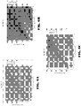
- FIGS. 6A-6C show examples of gain-voltage maps obtained by tuning laser mirror currents of a tunable laser at three different temperatures (e.g., 20°C, 30°C, and 40°C).
- the three different temperatures may be referred to as the calibration temperatures.
- tuning points or wavelengths are identified using one or more calibration algorithms, such as algorithms described in U.S. Patent Application Ser. No. 62/073,713 , and its corresponding utility patent application, for each map and loaded into the FPGA.
- FIG. 6A illustrates an example of a gain-voltage map which is obtained by tuning laser mirror currents of a tunable laser having two mirrors at a temperature of 20°C.
- the gain-voltage map is generated by observing optical output power as values of two mirror currents are varied. Further, all the minima of the gain-voltage map may be identified, via various processing, as points where the tunable laser is outputting a maximum power, and thus associated wavelengths may be extracted. The extracted wavelengths (or lasing wavelength peaks) may be used for tuning and calibrating processes of the tunable laser.
- corresponding gain-voltage maps may be generated respectively as shown in FIGS. 6B and 6C . In the example, it is noted that the gain-voltage maps are different based on the temperature values.
- the automatic wavelength mapping process may be implemented as a concurrent, independent module or process in the field programmable device 103 or 531, and may be configured to enable control loops to use data at different calibration temperatures.
- the adjustment of tuning currents for the laser mirrors may be done using one or more algorithms, and points from the tuning maps (or the gain-voltage maps) are described in more detail below as well as shown in FIGS. 7A and 7B . From the gain-voltage maps, the temperature dependence of the mirror currents may be estimated and analytical approximations may be derived. The temperature dependence of the mirror currents may then be derived from three or less gain-voltage maps taken at different temperatures given detailed knowledge of the tunable laser itself.
- the characteristics of the mirror currents, I mirror as a function of temperature t , can be accurately approximated by a second order polynomial equation as shown below.
- I mirror t a t 2 + bt + c
- a, b and c are constants that may or may not be specific to a given wavelength and t is the temperature of the laser. Therefore, each channel may or may not require additional parameters associated with it to accurately apply mirror currents with varying temperature.
- FIGS. 7A and 7B an example of tuning approximations for the two laser mirror currents at 1542.02 nm and 1577.16 nm wavelengths versus temperature is provided.
- mirror currents one can observe a continuous current over 30 °C on the left curve and a wrap-around scenario where one mirror current exceeds that maximum allowed current and wraps around as a curve, as shown in a bottom part of FIG. 7B .
- the latter is in some cases not desirable and thus the continuous example on the left may be the only feasible option for use.
- FIGS. 6A-6C different gain-voltage maps are observed over different temperatures.
- Various aspects of the automatic wavelength mapping, tuning and calibration of the tunable laser, as described herein, may be implemented as one or more concurrent, independent modules or processes in the field programmable device 103 or 531, and subsequently be configured to use data (e.g., data relating to the lasing wavelengths and others) at different calibration temperatures.
- the gain-voltage maps observed at the different temperatures may be used to determine lasing wavelengths at the different temperatures of the tunable laser.
- the temperatures of the tunable laser in the field may be adaptively changed via one or more currently running processes in the field programmable device or by control through one or more graphical user interfaces described below.
- the laser mirror currents may be automatically adapted based on the gain-voltage maps at different temperatures (also referred to herein as the laser mirror currents adaptation).
- a remote operator may have complete control of parameter settings of the tunable laser, via various graphical user interfaces (GUIs) configured to communicate through embedded processes in the field programmable device 103 or 531 (e.g., FPGA or PLD or the like) to the laser current and temperature settings of the tunable laser.
- GUIs graphical user interfaces
- the remote operator may change various parameter settings at different temperature settings and observe optical output spectra.
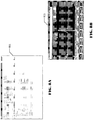
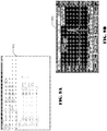
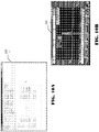
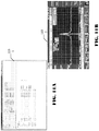
- FIGS. 8A-11B show GUIs that may be configured to control the laser current and temperature settings at 23 °C, 30 °C and 40 °C, with respective output spectra under the control of an operator via the GUIs.
- the GUI function may be integrated in the field programmable device or a system including the field programmable device, connected to the system via one or more wireless techniques, or connected to the system over optical transmission line(s) from a remote site or location.
- the GUI control function may be performed at the system via one or more communication interfaces including API, I2C, GPIO, or etc. of an optical transmitter (or transceiver).
- one or more control signals may be supplied from a GUI of the system, a GUI connected to the system via one or more wireless techniques, or a GUI connected to the system over optical transmission line(s) where the one or more control signals come from a GUI of another system at a remote site.
- the optical receiver of the system may read or decode input signals directly to control a wavelength of the system.
- the one or more control signals from the GUI of another system at the remote site may be received and decoded by a host coupled to the system and subsequently issue one or more commands to control the wavelength of the system.
- FIG. 8A illustrates laser current and temperature settings from GUI control 831 for a temperature value of 23 °C with laser mirror current adaptation enabled, and FIG. 8B shows its corresponding optical spectrum output 833.
- FIG. 9A illustrates laser current and temperature settings from GUI control 931 for a temperature value of 30 °C without laser mirror current adaptation, and FIG. 9B shows its corresponding optical spectrum output 933.
- FIG. 10A illustrates laser current and temperature settings from GUI control 1031 for a temperature value of 30 °C with laser mirror current adaptation enabled, and FIG. 10B shows its corresponding optical spectrum output 1033.
- FIG. 11A illustrates laser current and temperature settings from GUI control 1131 for a temperature value of 40 °C with laser mirror current adaptation enabled, and FIG. 11B shows its corresponding optical spectrum output 1133.
- the present disclosure may provide the operator at a remote location (e.g., at a host device) with enhanced capability to control various parameter settings of the tunable laser, as well as operational parameters relating to one or more processes concurrently running in the field programmable device, via the one or more GUIs as shown in FIGS. 8A , 9A , 10A , and 11A .
- a linewidth reduction algorithm may be digitally implemented as a concurrent, independent module or process in the field programmable device 103 or 531, such as the FPGA, PLD, or the like.
- the linewidth reduction algorithm such as the Pound-Drever-Hall (PDH) technique is a widely used and powerful approach for stabilizing the frequency of light from tunable lasers by locking to a stable cavity.
- the range of applications for the PDH technique is broad and may include interferometric gravitational wave detectors, atomic physics, and time measurement standards, many of which also use related techniques such as frequency modulation spectroscopy.
- FIG. 12 illustrates a typical implementation of an analog PDH control system.
- the emitted light from a laser 1201 is split by a splitter 1211 by some ratio and a part is phase modulated using an external clock source 1213.
- the phase modulated signal is sent through a circulator 1215 and to a Fabry-Perot filter 1217, and the reflected light from the Fabry-Perot filter 1217 is detected by a photodetector 1221 and subsequently mixed with an original clock source signal to generate an error signal 1223.
- the error signal 1223 is then signal processed and used on the laser to rectify phase aberrations, thus reducing its linewidth.
- a PDH feedback loop may be implemented as a concurrent, independent module or process in the field programmable device for high bit rate coherent communications as shown in FIG. 13 .
- control circuitry may be implemented as a concurrent, independent module or process in the field programmable device 103 or 531, such as the FPGA, PLD or the like, running at a clock speed independent of other control loop processes and optimized for a desired linewidth.
- the same optics, optoelectronics, analog electronics and analog-to-digital circuits used for other purposes, e.g., a wavelength locker 1323 may also be dual used for the linewidth narrowing, e.g., PHD circuit 1325, thereby reducing the cost, complexity, size, weight and power of a low linewidth transceiver or transmitter, which may be implemented in accordance with an aspect of the present disclosure.
- PHD circuit 1325 e.g., a low linewidth transceiver or transmitter, which may be implemented in accordance with an aspect of the present disclosure.
- all of the building blocks of the analog PDH control system illustrated in FIG. 12 may be implemented in reprogrammable hardware gates of the field programmable device 103 or 531.
- An illustration of a PDH linewidth control system that re-uses (dual use) wavelength locker components is shown in FIG. 13 with the PIC, external components and the PDH control loop.
- PDH algorithms use analog electronics to form the filtering, demodulation and feedback portions of a noise reduction loop. These functions may be problematic to perform in a microprocessor or a microcontroller, due to certain requirements for fixed low latency in a path from a detector to a laser phase modulator.
- advantages of the present technology may provide that the field programmable device 103 0r 531 enables implementations of digital signal processing (DSP) functions as fixed, dedicated modules or processes, allowing precise control of latency.
- DSP digital signal processing
- the implementation of the PDH feedback loop in accordance with the present disclosure may result in immunity from analog noise and electronic magnetic interference (EMI) sources and programmability which greatly simplifies calibration and optimization of feedback loop characteristics and linewidth reduction performance.
- EMI analog noise and electronic magnetic interference
- FIG. 14 shows an example block diagram illustrating one embodiment showing connections of a field programmable device (e.g., FPGA or PLD or the like) to ADC, DACs, laser and optical path, in accordance with an aspect of the present disclosure.
- FIG. 15 shows an example block diagram illustrating implementation of filtering function(s) embedded in a field programmable device for the PDH loop, in accordance with an aspect of the present disclosure.
- the detected optical power from a reflected etalon optical path is digitized and fed into the field programmable device such as an FPGA 1531, which is configured to perform the PDH algorithm filtering, demodulation, and produce an error cancellation signal that drives the laser phase modulator in a photonic integrated circuit (PIC) 1535.
- the FPGA 1531 is also configured to produce a reference modulation frequency that drives an etalon input optical signal phase modulator through a DAC, as shown in FIG. 15 .
- an equation for the detected power from the etalon reflected optical signal represented as a function of a difference between the reference modulation frequency and a representative unwanted frequency component may be derived and used, as shown in FIG. 16 .
- the detected power (P) includes three components, a DC term 1601, a component at a modulation frequency (error signal 1603), and a component at twice the modulation frequency (diagnostic 1605).
- the component at twice (2x) the modulation frequency (diagnostic 1605) may be used for test and calibration of a system.
- an amplitude of the component at the modulation frequency (error signal 1603) is proportional to a difference between any extraneous frequency components and the modulation frequency, and responds oppositely to positive and negative phase perturbations, thus producing a desired error signal.
- the error signal may be extracted and fed back to the phase modulator in the tunable laser to cancel undesired components as shown in FIG. 17 .
- ADC interface logic receives a digitized power signal from the etalon reflected optical path detector.
- a digital FIR band pass filter centered at the modulation frequency removes the DC component and 2x modulation frequency components from the detected power signal.
- the band pass output is then multiplied by the modulation frequency reference, which is generated by a DDS. The result is a demodulated error signal with a component at 2x modulation frequency which is unwanted.
- a FIR low pass filter with cutoff at about the modulation frequency removes the unwanted 2x modulation frequency component, while leaving any error components up to the modulation frequency.
- the resulting error signal goes through gain and offset blocks to provide proper amplitude and DC offset to drive the laser phase modulator, and then goes to the DAC interface logic which formats the data and sends it to the DAC.
- the design latency in the example path shown between the detected power from the etalon and the laser phase electrode, including the external ADC and DAC is less than 500 ns, the main contribution being from the FIR filters. Optimization of the foregoing algorithm may result in even lower latency.
- the reference DDS provides phase adjustment of the modulator reference signals sent to both the demodulator and the reference phase modulator such that the response can be nulled for initial calibration.
- Gain and offset adjustment are also provided for the reference modulation output.
- FIR filter coefficients, reference frequency and phase, gains, and offsets are all programmable by the host, enabling ease of algorithm optimization, tuning and calibration of the tunable laser and it associated systems.
- the linewidth reduction algorithm may be digitally implemented as a concurrent, independent module or process in the field programmable device 103 or 531, such as the FPGA, PLD, or the like.
- the present technology enables such large scale production of tunable lasers.
- parallel architectures that may be created using field programmable devices, such as FPGAs or PLDs or the like, enable monitoring of the critical parameters and feed them back to multiple control loops simultaneously with minimal latency, whereas a microprocessor or microcontroller would have to process and distribute all of the information in a serial and/or sequential manner.
- a field programmable device-centric implementation e.g., FPGA/PLD-centric implementation
- the field programmable device may be configured to control read cycles to a plurality of ADC channels, e.g., 24 ADC channels, such that the channel reads occur with minimal overhead and yet are fully programmable as to sequence and frequency per channel.
- This aspect of the present disclosure may enable monitoring of parameters critical to real time control loops with frequencies high enough to provide data for real time controls, such as wavelength locking, power control and temperature control.
- Table 1 lists some of the real-time controls as well as calibration algorithms with representative parameters that need to be monitored for each and sample rates. [Table 1.
- one or more implementations based on field programmable devices may allow the flexibility to architect the monitoring functions in a way that maximizes efficiency and allows all processes to obtain required data at sufficient rates simultaneously.
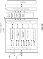
- FIG. 18 illustrates an example block diagram of firmware control of a field programmable device 1831, e.g., FPGA/PLD firmware, and attached ADCs and DACs 1833 that are used for monitoring parameters.
- all real time control loops may be configured to run in parallel with independent rates, e.g., independent clock rates (for example, 10Khz, 6.25Khz, 100Mhz, 1Khz, and 20Mhz in FIG. 18 ).
- Parameters required by the real time control loops may be supplied by monitor and control logic 1835, which may be configured to access parameters through one or more SPI busses 1837 interfaced to ADCs, DACs and other devices.
- the field programmable device 1831 e.g., FPGA, PLD, or the like, is configured to allow creating multiple SPI interfaces, each with different protocols, for devices that need high priority access, while also maximizing bandwidth and running with near-zero overhead on the SPI interfaces shared by multiple devices.
- the parameters required by multiple control loops may be distributed simultaneously to all required functions, and the parameters that are required with high bandwidth by some functions but not others may be supplied from multiple monitoring devices, as required.
- the real time control functions may be implemented in the field programmable device 1831 as one or more concurrent, independent processes in the field programmable device 1831, and thus may be used to analyze the parameters received from the monitor and control logic 1835 and generate alarms and status which are fed back to a host via a host or register interface 1841 and/or discrete 1843.
- the generated alarms may include: (i) laser temperature yellow and red alarms; (ii) laser power yellow and red alarms; (iii) laser on; and (iv) lambda stable.
- the field programmable device 1831 may also allow the calculations and decision processes for alarms to run in parallel, minimizing the latency of reporting anomalous conditions to the host.
- a wavelength locking algorithm dynamically tunes a laser wavelength to maintain it at a precise set point over variations in operating conditions based on a response of a Fabry-Perot etalon.
- the etalon has peak responses at wavelengths and intervals coincident with standard ITU specifications, but in principle the wavelengths could be at any value or interval, depending on the design of the etalon.
- FIG. 19 shows an example of general etalon reflected and transmitted responses.
- the transmitted response 1901 has peaks at the wavelengths of interest, whereas the reflected response 1903 has minima at these same wavelengths.
- compromises may be made on the finesse, or sharpness of the etalon maxima and minima, lessening the precision with which wavelength locking may be performed.
- efficient measurement of etalon response and algorithmic processing of the measurements are enabled to improve the quality of the results.
- the laser is first tuned to near a correct wavelength by tuning the mirrors based on a pre-calibrated table of mirror current values and corresponding wavelengths.
- the wavelength locking algorithm then fine-tunes the wavelength by dithering a laser phase electrode current over a small range about a default pre-calibrated value and searching for peak and/or minimum response.
- the algorithm may be performed digitally by controlling a current DAC that drives the laser phase electrode, and monitoring the etalon response through ADCs.
- FIG. 20 shows an example of a block diagram illustrating another implementation of a wavelength locking algorithm, in accordance with an aspect of the present disclosure.
- the wavelength locking algorithm is performed digitally by controlling a current DAC 2051 that drives the laser phase electrode, and monitoring the etalon response through ADCs 2051.
- a phase dithering speed may be a compromise between obtaining updates to a phase offset, and hence an operating wavelength, at a sufficient rate, minimizing linewidth effects of the dithering.
- the example technique may step the phase at a 100 us rate.
- the amplitude of the dithering may also be a compromise between scanning over a wide enough range to capture the maximum/minimum and not scanning so far as to perpetuate a mode hop in the laser 2053.
- the scan amplitude (or range) in the example implementation may be programmable and may be set per wavelength based on calibration tables, but is generally in a range of +/- 1 mA of phase electrode current.
- the detected etalon transmitted and reflected powers (via detectors 2058 coupled to a circulator 2055 and a etalon 2057) received from the ADC 2059 are then processed through an averaging filter 2033 to reduce noise and smooth the response.
- the field programmable device 2031 such as the FPGA, PLD or the like is configured to facilitate filtering the transmitted and reflected power data in parallel.
- the algorithm attempts to find a maximum in the transmitted data and a corresponding minimum in the reflected data, via a maximum/minimum search 2035, based on finding the maximum/minimum value over a data set and verifying that it is in fact an inflection point by requiring a threshold exceedance above/below the minimum/maximum at points on both sides of the minimum/maximum in the scan.
- the average of the determined maximum and minimum points is then used as a new phase offset to be applied to the laser 2053 to set a fine adjustment of the wavelength.
- the new phase offset will be based on the inflection point successfully determined, or if neither a minimum nor maximum is determined, the data for the current scan is not used and the phase is not changed until a successful scan is obtained.
- the new phase offset is provided to a phase offset 2037 and to the laser 2053 via a DAC control 2039 and a current DAC 2051.
- the above wavelength locking algorithm may be implemented as one or more concurrent, independent processes in the field programmable device (103, 531, or the like), such as the FPGA, PLD or the like.
- phase modulation may be needed to achieve at least one or more of the following: (i) wavelength locking, (ii) linewidth reduction; and (iii) Brillioun scattering mitigation.
- the laser wavelength is tuned under control of the field programmable device such as the FPGA or PLD or the like, via a multichannel current DAC driving the laser electrodes, interfaced via SPI.
- the initial mirror and phase electrode currents for a commanded wavelength may be set via a lookup table, and a wavelength locking control loop may run continuously based on detected etalon power to maintain wavelength stability.
- the field programmable device e.g., FPGA, PLD, or the like
- real time control algorithms facilitates enhancements and optimization, as individual control loops can be tuned independently without impacting overall system performance and timeline.
- a process for temperature control of a tunable laser may be implemented as a concurrent, independent process in the field programmable device (e.g., FPGA/PLD) which is configured to run at a different clock signal from other processes.
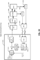
- FIG. 21 illustrates an example diagram of one implementation of the temperature control process.
- a module 2129 e.g., temp_pid
- the module 2129 monitors the TEC temperature, comparing it to the set temperature (e.g., temperature setpoint) and adjusting the TEC drive current to achieve the desired temperature.
- the TEC 2131 may be controlled through a linear control chip. As such, temperatures may be monitored via localized thermistors and selected ADC channel(s). TEC drive current may also be monitored via the linear control chip and selected ADC channel(s). TEC drive current may also be computed based on a PID loop output, the set temperature, and an actual TEC temperature. The PID loop output thus drives a selected DAC channel which determines the controller output current.
- the module 2129 (e.g., temp_pid) is configured to monitor and control an attached TEC 2131 through a TEC controller circuit 2135.
- the module 2129 may be configured to accept a desired temperature value as an input and servos at a settable rate (the time constant) until TEC actual temperature becomes the same as the set temperature.
- Maximum TEC current as well as maximum and minimum temperature may also be monitored for alarm conditions which are indicated with red and yellow alarm outputs.
- the structure of the ALU used to generate u(k) may consist of a 16x16 multiplier with a 4:1x16 mux on each input followed by a 36 bit summer with an accumulator register.
- a 16 bit substractor block produces the e(k) value.
- u(k) and u(k-1) are range checked and limited to x"1000" to avoid windup or overflow.
- the accumulator becomes the u(k-1) value for the next iteration.
- the input mux and multiplier and the ALU are all pipelined and it may take 2 clocks for the first product and sum and one clock each for the subsequent 3 multiply-and-adds. The accumulator then may hold u(k), which is u(k-1) for the next cycle.
- red alarm may indicate that either a maximum temperature, current, or temperature margin has been exceeded.
- a red alarm may cause a TEC shutdown and a laser shutdown.
- the PID constants and sample period may be estimating and set.
- the PID constants may be estimated using a Ziegler-Nichols method, which may require knowledge of a frequency at which the control loop will oscillate given sufficient gains without differential or integral terms. Further, due to safety limits imposed on the design, it may not be possible to obtain this value which requires steady state oscillation. Instead, Tu may be estimated from a damped oscillation period and Ku may be estimated.
- a simple first order model of the TEC (a single coefficient low pass filter) and the PID servo may be created in a spreadsheet with the discrete coefficients, a0 - a3 derived from the PID values.
- a step change in a set point for the temperature may generate a step response of the loop with the selected PID constants, Kp, Ki, and Kd, and the sample period Ts and the model transfer coefficient, "xfer_coeff".
- the response may be graphed so that the results may be viewed interactively.
- Actual coefficient inputs to the PID module may also be multiplied by 128, allowing for a binary point at bit 6 and fractional coefficients.
- the Ziegler-Nichols table may be implemented to give staring values for the PID constants given the estimates of Ku and Tu.
- the Ziegler-Nichols method may assign PID coefficients based on experimental data or simulated plant behavior using the following technique: • Set the Ki and Kd coefficients to zero. • Increase the Kp (gain) coefficient until the loop oscillates with a constant amplitude. • Note the period of oscillation --- this is Tu in the table below. • Note the Kp gain value ---- this is Ku, the ultimate gain in the table below.
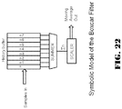
- one or more multichannel moving average (also known as "boxcar”) filters may be digitally implemented in the field programmable device (e.g., FPGA or PLD), which may be configured to provide configurable low pass filtering for each of 24 ADC channels in the 10G TOSA electronics board, for example.
- Each of the 24 channels may be set to a different filter depth of 0, 1, 2, 4, 8, 16, 32, 64, 128, or 256 samples. This capability may enable filtering of ADC output data where needed for short term fluctuations or random higher frequency noise.
- Filter depth and enable may also be programmed through a set of channel number associated registers in the register memory space. Before filtered output is determined to be valid, the sample memory for a given filter channel must be full of samples. As such, in one implementation, as the samples are taken, a sum of all the samples and the new sample minus the oldest sample may be averaged and presented as an output value of the filter.
- one or more boxcar filters may be implemented using internal memory blocks of the field programmable device (e.g., FPGA or PLD) for data history storage, addressing and indexing, and accumulating sums for each channel.
- the field programmable device e.g., FPGA or PLD
- a single 24-bit ALU in the field programmable device may be used for data summing and sums may be shifted right a number of positions appropriate for the depth of each filter. In one implementation, it may take approximately 10 system clock times from input to output (about 400 ns). Since a sample rate of an associated analog subsystem may be about 4 KHz/channel, the boxcar filter may easily accommodate all channels while adding very little delay time.
- a block diagram for a symbolic model of one channel of the boxcar filter is shown in FIG. 22 .
- a state of the registered memory map as well as device wavelength tables may be stored in one or more non-volatile flash memories (e.g., a Mcronix flash memory, MX25L4006E).
- Each flash memory may be a 4Mb capacity device and may be integral during the power-up of the device to apply the proper personality and in maintaining end user defined behavior of an entire system.
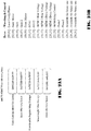
- An example of the address space of the non-volatile flash memory may be defined as shown in FIG. 23A .
- a wavelength definition table may be defined as shown in FIG. 23B .
- Each wavelength table may be a 32 byte structure, and each device may include storage space for a number of wavelength tables, whether internal or external to the field programmable device.
- on board firmware personality may undergo two procedures in order to place the device in a state determined by an end user.
- the procedures may include a loading of the registered memory map into a firmware system and a copying of the wavelength tables into RAM storage of the communication system.
- Each of the memory spaces may be defined as 4096 bytes (4KB).
- the register memory map may begin at 0x70000.
- the first procedure performed by the on board firmware personality is to copy the register values into the firmware register space.
- the second procedure performed is the copying of the wavelength tables from the flash beginning at 0x71000 into the wavelength RAM space on the device.
- the register value for a "current wavelength” is read by the device, and that wavelength is written to the laser electrode registers.
- the device may be fully powered up and configured, with the selected wavelength loaded and ready for operation. In the implementation, it may take approximately 0.4 ms to copy all of the register and wavelength data from the flash storage device.
- API Application Programming Interface
- the Applications Programming Interface may be implemented by DLL executable libraries.
- DLL executable libraries By importing the API DLLs into a coding project, a user of the API may have access to functions that control a tunable laser control electronics.
- the API functions available to the user may allow one to properly open a serial communications port, read and write to the register interface, and even provide some higher level macro functions to directly read the device temperature, set electrode currents, read monitor voltages, set a wavelength, and turn the laser and laser TEC on and off.
- the present disclosure may provide software-enabled features accessible via the APIs, offering extensive real-time control and monitoring of one or more modules or processes based on, for example, actual traffic flows.
- such programmability provides an unprecedented level of flexibility and responsiveness at an optical layer with real-time scaling and rerouting of a bandwidth, a higher bandwidth extraction from a given fiber plant as well as a reduction in complexity and related cost of planning, building, operating and maintaining data networks.
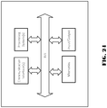
- the host controller 101, field programmable device 103, or laser 109 may be implemented with a bus architecture, which may include a bus and any number of interconnecting buses and bridges, as shown in FIG. 24 .
- the bus links together various circuits including one or more processing systems, one or more memories, one or more communication interfaces, and input/output devices.
- the one or more processing systems are responsible for managing the bus and general processing, including the execution of software stored on the non-transitory computer-readable medium.
- the one or more processing systems may include one or more reconfigurable circuit blocks that interpret and execute instructions.
- the one or more processing systems may be implemented as or include one or more application specific integrated circuits, field programmable logic arrays, or the like.
- the software when executed by the one or more processing systems, causes the one or more processing systems to perform the various functions described herein for any particular apparatus.
- the non-transitory computer-readable medium may also be used for storing data that is manipulated by the one or more processing systems when executing software.
- the one or more memories may include various types of memories including a random access memory or a read only memory, and/or other types of magnetic or optical recording medium and its corresponding derive for storing information and/or instructions.
- the one or more input/output devices may include devices that permit inputting information and/or outputting information to an external device or equipment.
- the one or more communication interfaces may also include any transceiver like mechanism that enables communication with other devices and/or systems, including optical transceivers (e.g., TOSA and/or ROSA).
- the term "software,” “module,” or “process” used herein is to be construed broadly to mean any instructions, instruction sets, programs, subprograms, code, program code, software modules, applications, software packages, routines, objects, executables, threads of execution, procedures, functions, etc. including firmware, microcode, middleware, software, hardware description language, or the like.
- the software may include various types of machine instructions including instructions, code, programs, subprograms, software modules, applications, software packages, routines, subroutines, executables, procedures, functions, etc.
- the software may also refer to general software, firmware, middleware, microcode, hardware description language, or etc.
- the software may be stored on a computer-readable medium.
- Examples of a computer-readable medium may include a non-transitory computer-readable medium, such as, by way of example, an optical disk, a magnetic storage device, a digital versatile disk, a flash memory, random access memory (RAM), static random access memory (SRAM), synchronous dynamic random access memory (SDRAM), read only memory (ROM), a register, programmable ROM (PROM), erasable PROM (EPROM), electrically erasable PROM (EEPROM), a removable disk, a flash memory device, and any other suitable medium for storing software that may be accessed and read by a processor or a processing system. It is also appreciated that one skilled in the art will recognize how best to implement the described functionality relating to various functions that are to be implemented in one or more field programmable device standalone or in combination with one or more computing systems, depending upon a particular application within design constraints.
- unit means software, hardware, or any combinations thereof.
- a component may be implemented as a software component, a hardware component, or any combinations thereof, including a field programmable gate array (FPGA), digital logic, digital logic arrays, application specific integrated circuit (ASIC), digital signal processor (DSP), etc. or any combinations thereof.
- the component thus may include software components, task components, processes, procedures, functions, program code, firmware, micro-codes, circuits, data structures, tables, arrays, and variables.
- first may be used to describe various components, but the components are not limited by the above terms. The above terms are used only to discriminate one component from the other component. For example, without departing from the scope of the present disclosure, a second component may be referred to as a first component, and the first component may be referred to as the second component in a similar manner. Also, the term “and/or” used herein includes a combination of a plurality of associated items or any item of the plurality of associated items.
- an element when it is described that an element is “coupled” or “connected” to another element, the element may be directly coupled or directly connected to the other element, or the element may be coupled or connected to the other element through a third element.
- a singular form may include a plural form if there is no clearly opposite meaning in the context.
- the term “include” or “have” used herein indicates that a feature, an operation, a component, a step, a number, a part or any combination thereof described herein is present.
- the term “include” or “have” does not exclude a possibility of presence or addition of one or more other features, operations, components, steps, numbers, parts or combinations.
- the article “a” is intended to include one or more items.
- no element, act, step, or instruction used in the present disclosure should be construed as critical or essential to the present disclosure unless explicitly described as such in the present disclosure.
Landscapes
- Physics & Mathematics (AREA)
- Electromagnetism (AREA)
- Engineering & Computer Science (AREA)
- Computer Networks & Wireless Communication (AREA)
- Signal Processing (AREA)
- Optics & Photonics (AREA)
- Condensed Matter Physics & Semiconductors (AREA)
- General Physics & Mathematics (AREA)
- Optical Modulation, Optical Deflection, Nonlinear Optics, Optical Demodulation, Optical Logic Elements (AREA)
- Optical Communication System (AREA)
- Semiconductor Lasers (AREA)
Claims (15)
- Vorrichtung zum Steuern, Überwachen und/oder Kommunizieren mit einer optischen Einrichtung, einer photonischen integrierten Schaltung oder einer Unterbaugruppe, wobei die Vorrichtung Folgendes umfasst:eine optische Einrichtung einschließlich eines abstimmbaren Lasers (109) mit zwei Spiegeln; undeine feldprogrammierbare Einrichtung (103) einschließlich programmierbaren Hardware-Gates, die mit der optischen Einrichtung gekoppelt sind, dadurch gekennzeichnet, dass:die feldprogrammierbare Einrichtung (103) ausgebildet ist, als eine Steuereinrichtung für die Vorrichtung zu agieren und mehrere Funktionen an einer Gate-Ebene zum Steuern, Überwachen und/oder Kommunizieren mit der optischen Einrichtung zu implementieren, wobei jede der mehreren Funktionen ausgebildet ist, als ein gleichzeitiger Prozess innerhalb der feldprogrammierbaren Einrichtung (103) ausgeführt zu werden;die mehreren Funktionen Funktionen zum Erhalten einer oder mehrerer Verstärkung-Spannung-Abbildungen beinhalten, indem Laserspiegelströme des abstimmbaren Lasers (109) bei einem Temperaturwert abgestimmt werden; unddie mehreren Funktionen ferner Funktionen zum Bestimmen von Laserwellenlängen beinhalten, die Minima der einen oder der mehreren Verstärkung-Spannung-Abbildungen gemäß einer Temperatur entsprechen, wobei die Laserwellenlängen zum Abstimmen oder Kalibrieren des abstimmbaren Lasers (109) der optischen Einrichtung verwendet werden.
- Vorrichtung nach Anspruch 1, wobei die mehreren Funktionen ausgebildet sind, bei unterschiedlichen Taktsignalen in der feldprogrammierbaren Einrichtung (103) ausgeführt zu werden.
- Vorrichtung nach Anspruch 1, wobei die Minima der einen oder der mehreren Verstärkung-Spannung-Abbildungen als Punkte einer maximalen Leistungsausgabe des abstimmbaren Lasers (109) bestimmt werden.
- Vorrichtung nach Anspruch 1, wobei die feldprogrammierbare Einrichtung (103) ausgebildet ist, ein oder mehrere Elemente der optischen Einrichtung zu steuern, die aus der Gruppe ausgewählt werden, die aus einem optischen Datenmodulator/-demodulator, internen oder externen optischen und optoelektronischen Überwachungs- und Steuerfunktionen besteht.
- Vorrichtung nach Anspruch 4, wobei die feldprogrammierbare Einrichtung (103) ein oder mehrere feldprogrammierbare Gate-Arrays (FPGAs) oder programmierbare Logikeinrichtungen (PLDs) umfasst.
- Vorrichtung nach Anspruch 1, wobei die feldprogrammierbare Einrichtung (103) ausgebildet ist, Lasersteuerströme des abstimmbaren Lasers (109) automatisch anzupassen, um eine Temperatur zu messen, sodass eine Last an einem thermoelektrischen Kühler (TEC) verringert wird, basierend auf der gemessenen Temperatur und mindestens einem der Folgenden: indem sich zwischen Tabellen, die in der feldprogrammierbaren Einrichtung (103) gespeichert sind, bewegt wird oder zwischen Temperatur-Wellenlängen-Abbildungen extrapoliert wird.
- Vorrichtung nach Anspruch 1, wobei die feldprogrammierbare Einrichtung (103) ausgebildet ist, eine oder mehrere Funktionen auszuführen, die aus der Gruppe ausgewählt werden, die aus Folgendem besteht:(i) Steuern und/oder Überwachen einer Laserausgangsleistung des abstimmbaren Lasers (109);(ii) Steuern und/oder Überwachen von temperaturempfindlichen Komponenten in Verbindung mit der optischen Einrichtung;(iii) Steuern und/oder Überwachen einer Laserwellenlänge des abstimmbaren Lasers (109);(iv) Steuern einer Wellenlängenkopplungsfunktion; und(v) Steuern und/oder Überwachen einer oder mehrerer Kommunikationsschnittstellen, die mit einem Host gekoppelt sind.
- Vorrichtung nach Anspruch 1, wobei die optische Einrichtung eine Kommunikationsschnittstelle umfasst, die in der feldprogrammierbaren Einrichtung (103) integriert ist, vorzugsweise wobei die programmierbare Einrichtung ein feldprogrammierbares Gate-Array (FPGA) umfasst.
- Vorrichtung nach Anspruch 8, wobei die Kommunikationsschnittstelle eine oder mehrere Anschlüsse zu einer grafischen Benutzeroberfläche (GUI) oder einer Anwendungsprogrammierungsschnittstelle (API), die ein Steuern, Überwachen und/oder eine Kommunikation mit dem abstimmbaren Laser (109) ermöglicht, einen optischen Datenmodulator/-demodulator oder andere optische oder optoelektronische Elemente, die monolithisch integriert sind, umfasst.
- Vorrichtung nach Anspruch 9, wobei eine Softwareschicht verwendet wird, um mit dem abstimmbaren Laser (109) über die feldprogrammierbare Einrichtung (103) zu interagieren, sodass ein schneller Wellenlängenkalibrationsalgorithmus implementiert wird.
- Vorrichtung nach Anspruch 1, wobei die feldprogrammierbare Einrichtung (103) ausgebildet ist, eine Temperaturabhängigkeit der Spiegelströme des abstimmbaren Lasers (109) basierend auf der einen oder den mehreren Verstärkung-Spannung-Abbildungen zu bestimmen und die Laserspiegelströme basierend auf der einen oder den mehreren Verstärkung-Spannung-Abbildungen bei unterschiedlichen Temperaturen automatisch anzupassen.
- Vorrichtung nach Anspruch 1, wobei die mehreren Funktionen einen Pound-Drever-Hall(PDH)-Algorithmus zum Verringern einer Linienbreite und/oder Stabilisieren einer Frequenz von Licht vom abstimmbaren Laser (109) der optischen Einrichtung beinhalten.
- Vorrichtung nach Anspruch 12, wobei der PDH-Algorithmus in umprogrammierbaren Hardware-Gates der feldprogrammierbaren Einrichtung (103) implementiert wird und manche der umprogrammierbaren Hardware-Gates zum Implementieren einer Wellenlängenkopplungsfunktion verwendet werden.
- Vorrichtung nach Anspruch 13, wobei die umprogrammierbaren Hardware-Gates der feldprogrammierbaren Einrichtung (103) ausgebildet sind, mindestens eines der Folgenden zu implementieren: Host-Kommunikationsschnittstellen, eine Speicherabbildung, Wellenlängenspeicher und -verwaltung, PROM-SPI-Flash-Schnittstelle (PROM - programmierbare Nurlesespeicher, SPI - serielle Peripherieschnittstelle) zu einem externen löschbaren programmierbaren Nurlesespeicher (EPROM), eingestellte Ströme und Spannungen für die optische Einrichtung, Überwachen von optischen und elektronischen Komponenten, Boxcar-Mittelwertbildner, automatische Leistungssteuerung, Wellenlängenkopplung, Linienbreiteneinengungsalgorithmen, Temperaturüberwachung und -steuerung, Alarmerzeugung, Überwachung, Steuerung und Kommunikation von Status und anwendungsprogrammierbare Schnittstellen.
- Vorrichtung nach Anspruch 1, wobei die feldprogrammierbare Einrichtung (103) ausgebildet ist, eine oder mehrere Steuersignale von einer grafischen Benutzeroberfläche (GUI), die mit der Vorrichtung über Drahtlosverbindungen gekoppelt ist, oder von einer GUI einer anderen Vorrichtung, die sich an einem entfernten Ort befindet, über eine optische Kommunikationsverbindung zu empfangen.
Applications Claiming Priority (2)
| Application Number | Priority Date | Filing Date | Title |
|---|---|---|---|
| US201462082545P | 2014-11-20 | 2014-11-20 | |
| PCT/US2015/061997 WO2016081906A1 (en) | 2014-11-20 | 2015-11-20 | Method and apparatus for controlling, monitoring, and communicating with tunable optical devices and subassemblies |
Publications (2)
| Publication Number | Publication Date |
|---|---|
| EP3221985A1 EP3221985A1 (de) | 2017-09-27 |
| EP3221985B1 true EP3221985B1 (de) | 2019-01-09 |
Family
ID=54838434
Family Applications (1)
| Application Number | Title | Priority Date | Filing Date |
|---|---|---|---|
| EP15807748.7A Active EP3221985B1 (de) | 2014-11-20 | 2015-11-20 | Verfahren und vorrichtung, zur steuerung, überwachung und kommunikation mit abstimmbaren optischen vorrichtungen und baugruppen |
Country Status (6)
| Country | Link |
|---|---|
| US (1) | US9722705B2 (de) |
| EP (1) | EP3221985B1 (de) |
| JP (1) | JP6602862B2 (de) |
| KR (1) | KR101916849B1 (de) |
| CN (1) | CN107210819B (de) |
| WO (1) | WO2016081906A1 (de) |
Families Citing this family (19)
| Publication number | Priority date | Publication date | Assignee | Title |
|---|---|---|---|---|
| GB2539414A (en) * | 2015-06-15 | 2016-12-21 | Oclaro Tech Ltd | Calibration of pluggable optical module |
| US10162632B1 (en) * | 2016-05-27 | 2018-12-25 | Cadence Design Systems, Inc. | System and method for a low-power processing architecture |
| US11249260B2 (en) | 2016-07-14 | 2022-02-15 | Ayar Labs, Inc. | Chip-to-chip optical data communication system |
| CN107516816A (zh) * | 2017-09-22 | 2017-12-26 | 北京航天计量测试技术研究所 | 一种连续线性调频激光光源 |
| CN111201684B (zh) * | 2017-12-15 | 2023-07-25 | 株式会社堀场制作所 | 半导体激光装置及其驱动方法、气体分析装置和存储介质 |
| JP7110715B2 (ja) * | 2018-05-14 | 2022-08-02 | オムロン株式会社 | モータ制御装置および設定装置 |
| JP7172126B2 (ja) * | 2018-05-14 | 2022-11-16 | オムロン株式会社 | モータ制御装置 |
| KR102170174B1 (ko) * | 2018-06-28 | 2020-10-28 | 단국대학교 천안캠퍼스 산학협력단 | 다파장 레이저다이오드의 빔 컴바이너, 그 빔 컴버이너 제어 장치 및 방법 |
| JP7502201B2 (ja) * | 2019-02-14 | 2024-06-18 | 古河電気工業株式会社 | 波長可変光源装置および波長可変レーザ素子の制御方法 |
| BE1027087B1 (fr) * | 2019-03-05 | 2020-10-05 | Skylane Optics Sa | Dispositif, systeme et kit de configuration d’emetteur-recepteur optique |
| CN114402241A (zh) * | 2019-07-24 | 2022-04-26 | 埃亚尔实验室公司 | 芯片到芯片光学数据通信系统 |
| US10785068B1 (en) * | 2019-11-06 | 2020-09-22 | Inphi Corporation | Systems and methods for relative intensity noise cancelation |
| US11782400B2 (en) * | 2019-12-17 | 2023-10-10 | The Hong Kong University Of Science And Technology | Indirect feedback tuning apparatuses and methods for tuning photonic systems |
| ES2752086B2 (es) * | 2019-12-18 | 2020-08-07 | Univ Politècnica De València | Dispositivo fotonico integrado de matriz cuantica de puertas fotonicas programables en campo, dispositivo quantico y circuitos programables |
| CN112181896B (zh) * | 2020-09-25 | 2024-03-29 | 加特兰微电子科技(上海)有限公司 | 运行控制设备、集成电路、无线电器件以及设备 |
| JP7572875B2 (ja) * | 2021-02-24 | 2024-10-24 | 株式会社ミツトヨ | 測定装置及び測定方法 |
| WO2023150598A2 (en) * | 2022-02-04 | 2023-08-10 | Stable Laser Systems, Inc. | Laser frequency stabilization |
| CN117438419B (zh) * | 2022-07-11 | 2025-08-08 | 上海曦智科技有限公司 | 半导体封装以及半导体封装的数据传输方法 |
| KR102839147B1 (ko) * | 2023-02-15 | 2025-07-28 | 한화시스템 주식회사 | 이득 광섬유 구조체용 손상 감지장치 및 이를 이용한 이득 광섬유 구조체의 화재 방지방법 |
Family Cites Families (27)
| Publication number | Priority date | Publication date | Assignee | Title |
|---|---|---|---|---|
| JP3585758B2 (ja) * | 1999-01-18 | 2004-11-04 | 富士通株式会社 | 利得等化のための方法並びに該方法の実施に使用する装置及びシステム |
| US6788719B2 (en) * | 2000-05-04 | 2004-09-07 | Agility Communications, Inc. | Open loop control of SGDBR lasers |
| US6690693B1 (en) * | 2000-05-04 | 2004-02-10 | Agility Communications, Inc. | Power and wavelength control of sampled grating distributed Bragg reflector lasers |
| US7061943B2 (en) * | 2000-06-29 | 2006-06-13 | Agility Communications, Inc. | Controller calibration for small form factor sampled grating distributed Bragg reflector laser |
| US6954476B2 (en) * | 2001-05-15 | 2005-10-11 | Agility Communications, Inc. | Sampled grating distributed Bragg reflector laser controller |
| US6631146B2 (en) * | 2001-07-06 | 2003-10-07 | Intel Corporation | Tunable laser control system |
| US6768827B2 (en) * | 2002-01-16 | 2004-07-27 | The Regents Of The University Of California | Integrated optical router |
| US6950450B2 (en) | 2002-12-18 | 2005-09-27 | Lucent Technologies Inc. | Control circuit for a tunable laser |
| US6917632B2 (en) * | 2002-12-31 | 2005-07-12 | Intel Corporation | Interrupt driven wavelength locking |
| US7009680B2 (en) * | 2003-06-02 | 2006-03-07 | Xtellus Inc. | Narrow band tunable filter with integrated detector |
| US20060072634A1 (en) | 2004-09-30 | 2006-04-06 | Daiber Andrew J | Calibration methods for tunable lasers |
| JP2006279246A (ja) * | 2005-03-28 | 2006-10-12 | Fujitsu Ltd | 光伝送装置およびその制御方法 |
| JP4957306B2 (ja) * | 2007-03-15 | 2012-06-20 | 住友電気工業株式会社 | 光送信器 |
| JP2009081512A (ja) * | 2007-09-25 | 2009-04-16 | Fujitsu Ltd | 光送信装置および設定値決定方法 |
| US7622952B1 (en) * | 2008-05-28 | 2009-11-24 | Altera Corporation | Periphery clock signal distribution circuitry for structured ASIC devices |
| US8644713B2 (en) | 2009-11-12 | 2014-02-04 | Packet Photonics, Inc. | Optical burst mode clock and data recovery |
| SE535247C2 (sv) | 2010-10-06 | 2012-06-05 | Syntune Ab | Förfarande för att kalibrera en avstämbar laser |
| US9595804B2 (en) * | 2011-07-22 | 2017-03-14 | Insight Photonic Solutions, Inc. | System and method of dynamic and adaptive creation of a wavelength continuous and prescribed wavelength versus time sweep from a laser |
| US8964806B2 (en) * | 2012-01-19 | 2015-02-24 | Insight Photonic Solutions, Inc. | System and method for generating an optimum side-mode suppression ratio continuous tuning path for a semiconductor tunable laser |
| EP2873175B1 (de) * | 2012-07-15 | 2023-05-17 | OE Solutions America Inc. | Steuersysteme für optische vorrichtungen und baugruppen |
| WO2014107537A1 (en) | 2013-01-02 | 2014-07-10 | Packet Photonics, Inc. | Tunable u-laser transmitter with integrated mach-zehnder modulator |
| US20140236527A1 (en) * | 2013-02-21 | 2014-08-21 | Advantest Corporation | Cloud based infrastructure for supporting protocol reconfigurations in protocol independent device testing systems |
| US9438347B2 (en) * | 2013-03-15 | 2016-09-06 | Sanmina Corporation | Optical media converter with edge-coupled filtering |
| CN103580757B (zh) * | 2013-09-26 | 2016-05-11 | 青岛海信宽带多媒体技术有限公司 | 光网络单元 |
| JP6281303B2 (ja) * | 2014-02-03 | 2018-02-21 | 富士通株式会社 | 多値強度変復調システムおよび方法 |
| US9485021B2 (en) * | 2014-07-25 | 2016-11-01 | Arris Enterprises, Inc. | Hybrid laser anti-clipping for fiber-coaxial networks |
| WO2016070142A1 (en) * | 2014-10-31 | 2016-05-06 | Oe Solutions America, Inc. | Fast calibration and programming optical components |
-
2015
- 2015-11-20 US US14/947,905 patent/US9722705B2/en active Active
- 2015-11-20 KR KR1020177016798A patent/KR101916849B1/ko active Active
- 2015-11-20 JP JP2017527218A patent/JP6602862B2/ja active Active
- 2015-11-20 EP EP15807748.7A patent/EP3221985B1/de active Active
- 2015-11-20 WO PCT/US2015/061997 patent/WO2016081906A1/en not_active Ceased
- 2015-11-20 CN CN201580063180.0A patent/CN107210819B/zh active Active
Non-Patent Citations (1)
| Title |
|---|
| None * |
Also Published As
| Publication number | Publication date |
|---|---|
| JP2018502485A (ja) | 2018-01-25 |
| US9722705B2 (en) | 2017-08-01 |
| CN107210819A (zh) | 2017-09-26 |
| EP3221985A1 (de) | 2017-09-27 |
| WO2016081906A1 (en) | 2016-05-26 |
| JP6602862B2 (ja) | 2019-11-06 |
| CN107210819B (zh) | 2020-12-22 |
| KR20170107969A (ko) | 2017-09-26 |
| KR101916849B1 (ko) | 2018-11-08 |
| US20160254866A1 (en) | 2016-09-01 |
Similar Documents
| Publication | Publication Date | Title |
|---|---|---|
| US9722705B2 (en) | Method and apparatus for controlling, monitoring, and communicating with tunable optical devices and subassemblies | |
| US6400737B1 (en) | Automatic closed-looped gain adjustment for a temperature tuned, wavelength stabilized laser source in a closed-loop feedback control system | |
| US6516010B1 (en) | Method and apparatus for active numeric temperature compensation of an etalon in a wavelength stabilized laser | |
| CN111712980B (zh) | 光模块、其波长控制方法以及其校准方法 | |
| US20020176452A1 (en) | Digital control of actively mode-locked lasers | |
| US11699891B2 (en) | Laser device | |
| US9543737B2 (en) | Fast calibration and programming optical components | |
| EP2227715A1 (de) | Bias-steuerung | |
| EP1291988A1 (de) | Frequenzverriegelung einer Mehrsektionslaserdiode | |
| US9742149B2 (en) | Method for controlling tunable wavelength laser | |
| Bailly et al. | High spectral purity optical source stabilized on a fiber ring resonator | |
| US20090086774A1 (en) | Control device, laser device, wavelength converting method, and program | |
| US7200159B2 (en) | Method and apparatus for temperature stabilization of a wavelength of a laser | |
| US11581700B1 (en) | Multiple optoelectronic devices with thermal compensation | |
| US11973304B1 (en) | Tunable laser | |
| WO2021100101A1 (ja) | 光周波数制御装置、光発振装置、周波数変換装置及び電波発生装置 | |
| KR20260038195A (ko) | 레이저 시스템 및 레이저 안정화 방법 | |
| US20130243014A1 (en) | Method for calibrating a tunable laser | |
| JP5845657B2 (ja) | 制御装置、光受信装置および制御方法 | |
| Portuondo-Campa et al. | Compact Hz-level linewidth laser system |
Legal Events
| Date | Code | Title | Description |
|---|---|---|---|
| STAA | Information on the status of an ep patent application or granted ep patent |
Free format text: STATUS: THE INTERNATIONAL PUBLICATION HAS BEEN MADE |
|
| PUAI | Public reference made under article 153(3) epc to a published international application that has entered the european phase |
Free format text: ORIGINAL CODE: 0009012 |
|
| STAA | Information on the status of an ep patent application or granted ep patent |
Free format text: STATUS: REQUEST FOR EXAMINATION WAS MADE |
|
| 17P | Request for examination filed |
Effective date: 20170614 |
|
| AK | Designated contracting states |
Kind code of ref document: A1 Designated state(s): AL AT BE BG CH CY CZ DE DK EE ES FI FR GB GR HR HU IE IS IT LI LT LU LV MC MK MT NL NO PL PT RO RS SE SI SK SM TR |
|
| AX | Request for extension of the european patent |
Extension state: BA ME |
|
| RAP1 | Party data changed (applicant data changed or rights of an application transferred) |
Owner name: OE SOLUTIONS AMERICA INC. |
|
| RIN1 | Information on inventor provided before grant (corrected) |
Inventor name: BLUMENTHAL, DANIEL, J. Inventor name: KLEIN, HOLGER Inventor name: CICCHI, TODD Inventor name: BYBEE, PATRICK Inventor name: POULSEN, HENRIK |
|
| DAV | Request for validation of the european patent (deleted) | ||
| DAX | Request for extension of the european patent (deleted) | ||
| GRAP | Despatch of communication of intention to grant a patent |
Free format text: ORIGINAL CODE: EPIDOSNIGR1 |
|
| STAA | Information on the status of an ep patent application or granted ep patent |
Free format text: STATUS: GRANT OF PATENT IS INTENDED |
|
| RIC1 | Information provided on ipc code assigned before grant |
Ipc: H04B 10/572 20130101ALI20180530BHEP Ipc: H01S 5/0687 20060101ALI20180530BHEP Ipc: H04B 10/50 20130101AFI20180530BHEP |
|
| INTG | Intention to grant announced |
Effective date: 20180615 |
|
| GRAS | Grant fee paid |
Free format text: ORIGINAL CODE: EPIDOSNIGR3 |
|
| GRAA | (expected) grant |
Free format text: ORIGINAL CODE: 0009210 |
|
| STAA | Information on the status of an ep patent application or granted ep patent |
Free format text: STATUS: THE PATENT HAS BEEN GRANTED |
|
| AK | Designated contracting states |
Kind code of ref document: B1 Designated state(s): AL AT BE BG CH CY CZ DE DK EE ES FI FR GB GR HR HU IE IS IT LI LT LU LV MC MK MT NL NO PL PT RO RS SE SI SK SM TR |
|
| REG | Reference to a national code |
Ref country code: GB Ref legal event code: FG4D |
|
| REG | Reference to a national code |
Ref country code: CH Ref legal event code: EP Ref country code: AT Ref legal event code: REF Ref document number: 1088637 Country of ref document: AT Kind code of ref document: T Effective date: 20190115 |
|
| REG | Reference to a national code |
Ref country code: IE Ref legal event code: FG4D |
|
| REG | Reference to a national code |
Ref country code: DE Ref legal event code: R096 Ref document number: 602015023360 Country of ref document: DE |
|
| REG | Reference to a national code |
Ref country code: NL Ref legal event code: MP Effective date: 20190109 |
|
| REG | Reference to a national code |
Ref country code: LT Ref legal event code: MG4D |
|
| PG25 | Lapsed in a contracting state [announced via postgrant information from national office to epo] |
Ref country code: NL Free format text: LAPSE BECAUSE OF FAILURE TO SUBMIT A TRANSLATION OF THE DESCRIPTION OR TO PAY THE FEE WITHIN THE PRESCRIBED TIME-LIMIT Effective date: 20190109 |
|
| REG | Reference to a national code |
Ref country code: AT Ref legal event code: MK05 Ref document number: 1088637 Country of ref document: AT Kind code of ref document: T Effective date: 20190109 |
|
| PG25 | Lapsed in a contracting state [announced via postgrant information from national office to epo] |
Ref country code: PT Free format text: LAPSE BECAUSE OF FAILURE TO SUBMIT A TRANSLATION OF THE DESCRIPTION OR TO PAY THE FEE WITHIN THE PRESCRIBED TIME-LIMIT Effective date: 20190509 Ref country code: SE Free format text: LAPSE BECAUSE OF FAILURE TO SUBMIT A TRANSLATION OF THE DESCRIPTION OR TO PAY THE FEE WITHIN THE PRESCRIBED TIME-LIMIT Effective date: 20190109 Ref country code: FI Free format text: LAPSE BECAUSE OF FAILURE TO SUBMIT A TRANSLATION OF THE DESCRIPTION OR TO PAY THE FEE WITHIN THE PRESCRIBED TIME-LIMIT Effective date: 20190109 Ref country code: LT Free format text: LAPSE BECAUSE OF FAILURE TO SUBMIT A TRANSLATION OF THE DESCRIPTION OR TO PAY THE FEE WITHIN THE PRESCRIBED TIME-LIMIT Effective date: 20190109 Ref country code: PL Free format text: LAPSE BECAUSE OF FAILURE TO SUBMIT A TRANSLATION OF THE DESCRIPTION OR TO PAY THE FEE WITHIN THE PRESCRIBED TIME-LIMIT Effective date: 20190109 Ref country code: NO Free format text: LAPSE BECAUSE OF FAILURE TO SUBMIT A TRANSLATION OF THE DESCRIPTION OR TO PAY THE FEE WITHIN THE PRESCRIBED TIME-LIMIT Effective date: 20190409 Ref country code: ES Free format text: LAPSE BECAUSE OF FAILURE TO SUBMIT A TRANSLATION OF THE DESCRIPTION OR TO PAY THE FEE WITHIN THE PRESCRIBED TIME-LIMIT Effective date: 20190109 |
|
| PG25 | Lapsed in a contracting state [announced via postgrant information from national office to epo] |
Ref country code: HR Free format text: LAPSE BECAUSE OF FAILURE TO SUBMIT A TRANSLATION OF THE DESCRIPTION OR TO PAY THE FEE WITHIN THE PRESCRIBED TIME-LIMIT Effective date: 20190109 Ref country code: GR Free format text: LAPSE BECAUSE OF FAILURE TO SUBMIT A TRANSLATION OF THE DESCRIPTION OR TO PAY THE FEE WITHIN THE PRESCRIBED TIME-LIMIT Effective date: 20190410 Ref country code: LV Free format text: LAPSE BECAUSE OF FAILURE TO SUBMIT A TRANSLATION OF THE DESCRIPTION OR TO PAY THE FEE WITHIN THE PRESCRIBED TIME-LIMIT Effective date: 20190109 Ref country code: IS Free format text: LAPSE BECAUSE OF FAILURE TO SUBMIT A TRANSLATION OF THE DESCRIPTION OR TO PAY THE FEE WITHIN THE PRESCRIBED TIME-LIMIT Effective date: 20190509 Ref country code: BG Free format text: LAPSE BECAUSE OF FAILURE TO SUBMIT A TRANSLATION OF THE DESCRIPTION OR TO PAY THE FEE WITHIN THE PRESCRIBED TIME-LIMIT Effective date: 20190409 Ref country code: RS Free format text: LAPSE BECAUSE OF FAILURE TO SUBMIT A TRANSLATION OF THE DESCRIPTION OR TO PAY THE FEE WITHIN THE PRESCRIBED TIME-LIMIT Effective date: 20190109 |
|
| REG | Reference to a national code |
Ref country code: DE Ref legal event code: R097 Ref document number: 602015023360 Country of ref document: DE |
|
| PG25 | Lapsed in a contracting state [announced via postgrant information from national office to epo] |
Ref country code: IT Free format text: LAPSE BECAUSE OF FAILURE TO SUBMIT A TRANSLATION OF THE DESCRIPTION OR TO PAY THE FEE WITHIN THE PRESCRIBED TIME-LIMIT Effective date: 20190109 Ref country code: EE Free format text: LAPSE BECAUSE OF FAILURE TO SUBMIT A TRANSLATION OF THE DESCRIPTION OR TO PAY THE FEE WITHIN THE PRESCRIBED TIME-LIMIT Effective date: 20190109 Ref country code: AT Free format text: LAPSE BECAUSE OF FAILURE TO SUBMIT A TRANSLATION OF THE DESCRIPTION OR TO PAY THE FEE WITHIN THE PRESCRIBED TIME-LIMIT Effective date: 20190109 Ref country code: CZ Free format text: LAPSE BECAUSE OF FAILURE TO SUBMIT A TRANSLATION OF THE DESCRIPTION OR TO PAY THE FEE WITHIN THE PRESCRIBED TIME-LIMIT Effective date: 20190109 Ref country code: RO Free format text: LAPSE BECAUSE OF FAILURE TO SUBMIT A TRANSLATION OF THE DESCRIPTION OR TO PAY THE FEE WITHIN THE PRESCRIBED TIME-LIMIT Effective date: 20190109 Ref country code: DK Free format text: LAPSE BECAUSE OF FAILURE TO SUBMIT A TRANSLATION OF THE DESCRIPTION OR TO PAY THE FEE WITHIN THE PRESCRIBED TIME-LIMIT Effective date: 20190109 Ref country code: AL Free format text: LAPSE BECAUSE OF FAILURE TO SUBMIT A TRANSLATION OF THE DESCRIPTION OR TO PAY THE FEE WITHIN THE PRESCRIBED TIME-LIMIT Effective date: 20190109 Ref country code: SK Free format text: LAPSE BECAUSE OF FAILURE TO SUBMIT A TRANSLATION OF THE DESCRIPTION OR TO PAY THE FEE WITHIN THE PRESCRIBED TIME-LIMIT Effective date: 20190109 |
|
| PLBE | No opposition filed within time limit |
Free format text: ORIGINAL CODE: 0009261 |
|
| STAA | Information on the status of an ep patent application or granted ep patent |
Free format text: STATUS: NO OPPOSITION FILED WITHIN TIME LIMIT |
|
| PG25 | Lapsed in a contracting state [announced via postgrant information from national office to epo] |
Ref country code: SM Free format text: LAPSE BECAUSE OF FAILURE TO SUBMIT A TRANSLATION OF THE DESCRIPTION OR TO PAY THE FEE WITHIN THE PRESCRIBED TIME-LIMIT Effective date: 20190109 |
|
| 26N | No opposition filed |
Effective date: 20191010 |
|
| PG25 | Lapsed in a contracting state [announced via postgrant information from national office to epo] |
Ref country code: SI Free format text: LAPSE BECAUSE OF FAILURE TO SUBMIT A TRANSLATION OF THE DESCRIPTION OR TO PAY THE FEE WITHIN THE PRESCRIBED TIME-LIMIT Effective date: 20190109 |
|
| PG25 | Lapsed in a contracting state [announced via postgrant information from national office to epo] |
Ref country code: TR Free format text: LAPSE BECAUSE OF FAILURE TO SUBMIT A TRANSLATION OF THE DESCRIPTION OR TO PAY THE FEE WITHIN THE PRESCRIBED TIME-LIMIT Effective date: 20190109 |
|
| REG | Reference to a national code |
Ref country code: CH Ref legal event code: PL |
|
| PG25 | Lapsed in a contracting state [announced via postgrant information from national office to epo] |
Ref country code: LU Free format text: LAPSE BECAUSE OF NON-PAYMENT OF DUE FEES Effective date: 20191120 Ref country code: MC Free format text: LAPSE BECAUSE OF FAILURE TO SUBMIT A TRANSLATION OF THE DESCRIPTION OR TO PAY THE FEE WITHIN THE PRESCRIBED TIME-LIMIT Effective date: 20190109 Ref country code: CH Free format text: LAPSE BECAUSE OF NON-PAYMENT OF DUE FEES Effective date: 20191130 Ref country code: LI Free format text: LAPSE BECAUSE OF NON-PAYMENT OF DUE FEES Effective date: 20191130 |
|
| REG | Reference to a national code |
Ref country code: BE Ref legal event code: MM Effective date: 20191130 |
|
| PG25 | Lapsed in a contracting state [announced via postgrant information from national office to epo] |
Ref country code: IE Free format text: LAPSE BECAUSE OF NON-PAYMENT OF DUE FEES Effective date: 20191120 |
|
| PG25 | Lapsed in a contracting state [announced via postgrant information from national office to epo] |
Ref country code: BE Free format text: LAPSE BECAUSE OF NON-PAYMENT OF DUE FEES Effective date: 20191130 |
|
| PG25 | Lapsed in a contracting state [announced via postgrant information from national office to epo] |
Ref country code: CY Free format text: LAPSE BECAUSE OF FAILURE TO SUBMIT A TRANSLATION OF THE DESCRIPTION OR TO PAY THE FEE WITHIN THE PRESCRIBED TIME-LIMIT Effective date: 20190109 |
|
| PG25 | Lapsed in a contracting state [announced via postgrant information from national office to epo] |
Ref country code: HU Free format text: LAPSE BECAUSE OF FAILURE TO SUBMIT A TRANSLATION OF THE DESCRIPTION OR TO PAY THE FEE WITHIN THE PRESCRIBED TIME-LIMIT; INVALID AB INITIO Effective date: 20151120 Ref country code: MT Free format text: LAPSE BECAUSE OF FAILURE TO SUBMIT A TRANSLATION OF THE DESCRIPTION OR TO PAY THE FEE WITHIN THE PRESCRIBED TIME-LIMIT Effective date: 20190109 |
|
| PG25 | Lapsed in a contracting state [announced via postgrant information from national office to epo] |
Ref country code: MK Free format text: LAPSE BECAUSE OF FAILURE TO SUBMIT A TRANSLATION OF THE DESCRIPTION OR TO PAY THE FEE WITHIN THE PRESCRIBED TIME-LIMIT Effective date: 20190109 |
|
| REG | Reference to a national code |
Ref country code: GB Ref legal event code: 732E Free format text: REGISTERED BETWEEN 20250213 AND 20250219 |
|
| REG | Reference to a national code |
Ref country code: DE Ref legal event code: R081 Ref document number: 602015023360 Country of ref document: DE Owner name: OE SOLUTIONS CO., LTD., KR Free format text: FORMER OWNER: OE SOLUTIONS AMERICA INC., RIDGEFIELD PARK, NJ, US |
|
| PGFP | Annual fee paid to national office [announced via postgrant information from national office to epo] |
Ref country code: DE Payment date: 20251117 Year of fee payment: 11 |
|
| PGFP | Annual fee paid to national office [announced via postgrant information from national office to epo] |
Ref country code: GB Payment date: 20251120 Year of fee payment: 11 |
|
| PGFP | Annual fee paid to national office [announced via postgrant information from national office to epo] |
Ref country code: FR Payment date: 20251125 Year of fee payment: 11 |