EP3218932B1 - Method of fabricating a pixelated scintillator with optimized efficiency - Google Patents
Method of fabricating a pixelated scintillator with optimized efficiency Download PDFInfo
- Publication number
- EP3218932B1 EP3218932B1 EP15790085.3A EP15790085A EP3218932B1 EP 3218932 B1 EP3218932 B1 EP 3218932B1 EP 15790085 A EP15790085 A EP 15790085A EP 3218932 B1 EP3218932 B1 EP 3218932B1
- Authority
- EP
- European Patent Office
- Prior art keywords
- sintering
- pixelated scintillator
- scintillator
- shrinking
- connection
- Prior art date
- Legal status (The legal status is an assumption and is not a legal conclusion. Google has not performed a legal analysis and makes no representation as to the accuracy of the status listed.)
- Active
Links
- 238000004519 manufacturing process Methods 0.000 title claims description 19
- 239000010410 layer Substances 0.000 claims description 63
- 238000000034 method Methods 0.000 claims description 46
- 238000005245 sintering Methods 0.000 claims description 43
- 239000000463 material Substances 0.000 claims description 37
- 239000011229 interlayer Substances 0.000 claims description 17
- 239000011248 coating agent Substances 0.000 claims description 11
- 238000000576 coating method Methods 0.000 claims description 11
- 239000000654 additive Substances 0.000 claims description 9
- 230000000996 additive effect Effects 0.000 claims description 9
- 229910010293 ceramic material Inorganic materials 0.000 claims description 7
- 239000002585 base Substances 0.000 description 39
- XQPRBTXUXXVTKB-UHFFFAOYSA-M caesium iodide Inorganic materials [I-].[Cs+] XQPRBTXUXXVTKB-UHFFFAOYSA-M 0.000 description 10
- FVAUCKIRQBBSSJ-UHFFFAOYSA-M sodium iodide Chemical compound [Na+].[I-] FVAUCKIRQBBSSJ-UHFFFAOYSA-M 0.000 description 9
- 238000010146 3D printing Methods 0.000 description 8
- 239000013067 intermediate product Substances 0.000 description 8
- 238000003384 imaging method Methods 0.000 description 6
- 239000004593 Epoxy Substances 0.000 description 5
- 239000013078 crystal Substances 0.000 description 4
- 230000008021 deposition Effects 0.000 description 4
- 239000002245 particle Substances 0.000 description 4
- 239000011230 binding agent Substances 0.000 description 3
- 239000000919 ceramic Substances 0.000 description 3
- 238000007641 inkjet printing Methods 0.000 description 3
- 235000009518 sodium iodide Nutrition 0.000 description 3
- 229910019655 synthetic inorganic crystalline material Inorganic materials 0.000 description 3
- 229910052716 thallium Inorganic materials 0.000 description 3
- BKVIYDNLLOSFOA-UHFFFAOYSA-N thallium Chemical compound [Tl] BKVIYDNLLOSFOA-UHFFFAOYSA-N 0.000 description 3
- -1 CdWO4 Inorganic materials 0.000 description 2
- 229910052688 Gadolinium Inorganic materials 0.000 description 2
- GWEVSGVZZGPLCZ-UHFFFAOYSA-N Titan oxide Chemical compound O=[Ti]=O GWEVSGVZZGPLCZ-UHFFFAOYSA-N 0.000 description 2
- 239000003513 alkali Substances 0.000 description 2
- 229910052782 aluminium Inorganic materials 0.000 description 2
- 150000001875 compounds Chemical class 0.000 description 2
- 230000001419 dependent effect Effects 0.000 description 2
- UIWYJDYFSGRHKR-UHFFFAOYSA-N gadolinium atom Chemical compound [Gd] UIWYJDYFSGRHKR-UHFFFAOYSA-N 0.000 description 2
- 238000000227 grinding Methods 0.000 description 2
- 238000010438 heat treatment Methods 0.000 description 2
- 230000005855 radiation Effects 0.000 description 2
- 239000000725 suspension Substances 0.000 description 2
- 229910052727 yttrium Inorganic materials 0.000 description 2
- VWQVUPCCIRVNHF-UHFFFAOYSA-N yttrium atom Chemical compound [Y] VWQVUPCCIRVNHF-UHFFFAOYSA-N 0.000 description 2
- 229910004829 CaWO4 Inorganic materials 0.000 description 1
- 229910052684 Cerium Inorganic materials 0.000 description 1
- GYHNNYVSQQEPJS-UHFFFAOYSA-N Gallium Chemical compound [Ga] GYHNNYVSQQEPJS-UHFFFAOYSA-N 0.000 description 1
- 229910052765 Lutetium Inorganic materials 0.000 description 1
- 229910052771 Terbium Inorganic materials 0.000 description 1
- 239000005083 Zinc sulfide Substances 0.000 description 1
- ANDNPYOOQLLLIU-UHFFFAOYSA-N [Y].[Lu] Chemical compound [Y].[Lu] ANDNPYOOQLLLIU-UHFFFAOYSA-N 0.000 description 1
- 239000012190 activator Substances 0.000 description 1
- 229910001508 alkali metal halide Inorganic materials 0.000 description 1
- 150000008045 alkali metal halides Chemical class 0.000 description 1
- 229910045601 alloy Inorganic materials 0.000 description 1
- 239000000956 alloy Substances 0.000 description 1
- 239000004411 aluminium Substances 0.000 description 1
- XAGFODPZIPBFFR-UHFFFAOYSA-N aluminium Chemical compound [Al] XAGFODPZIPBFFR-UHFFFAOYSA-N 0.000 description 1
- 229910001632 barium fluoride Inorganic materials 0.000 description 1
- 230000004888 barrier function Effects 0.000 description 1
- ORCSMBGZHYTXOV-UHFFFAOYSA-N bismuth;germanium;dodecahydrate Chemical compound O.O.O.O.O.O.O.O.O.O.O.O.[Ge].[Ge].[Ge].[Bi].[Bi].[Bi].[Bi] ORCSMBGZHYTXOV-UHFFFAOYSA-N 0.000 description 1
- WUKWITHWXAAZEY-UHFFFAOYSA-L calcium difluoride Chemical compound [F-].[F-].[Ca+2] WUKWITHWXAAZEY-UHFFFAOYSA-L 0.000 description 1
- 229910001634 calcium fluoride Inorganic materials 0.000 description 1
- 238000007707 calorimetry Methods 0.000 description 1
- ZMIGMASIKSOYAM-UHFFFAOYSA-N cerium Chemical compound [Ce][Ce][Ce][Ce][Ce][Ce][Ce][Ce][Ce][Ce][Ce][Ce][Ce][Ce][Ce][Ce][Ce][Ce][Ce][Ce][Ce][Ce][Ce][Ce][Ce][Ce][Ce][Ce][Ce][Ce][Ce][Ce][Ce][Ce][Ce][Ce][Ce][Ce] ZMIGMASIKSOYAM-UHFFFAOYSA-N 0.000 description 1
- 238000002059 diagnostic imaging Methods 0.000 description 1
- 239000012467 final product Substances 0.000 description 1
- 229910052733 gallium Inorganic materials 0.000 description 1
- 239000002223 garnet Substances 0.000 description 1
- 229910000204 garnet group Inorganic materials 0.000 description 1
- 150000004820 halides Chemical class 0.000 description 1
- 239000012535 impurity Substances 0.000 description 1
- 229910000765 intermetallic Inorganic materials 0.000 description 1
- 230000005865 ionizing radiation Effects 0.000 description 1
- OHSVLFRHMCKCQY-UHFFFAOYSA-N lutetium atom Chemical compound [Lu] OHSVLFRHMCKCQY-UHFFFAOYSA-N 0.000 description 1
- 238000009206 nuclear medicine Methods 0.000 description 1
- 238000002360 preparation method Methods 0.000 description 1
- 229910052761 rare earth metal Inorganic materials 0.000 description 1
- 150000002910 rare earth metals Chemical class 0.000 description 1
- 229910052604 silicate mineral Inorganic materials 0.000 description 1
- 229910052709 silver Inorganic materials 0.000 description 1
- 239000011734 sodium Substances 0.000 description 1
- GZCRRIHWUXGPOV-UHFFFAOYSA-N terbium atom Chemical compound [Tb] GZCRRIHWUXGPOV-UHFFFAOYSA-N 0.000 description 1
- DRDVZXDWVBGGMH-UHFFFAOYSA-N zinc;sulfide Chemical compound [S-2].[Zn+2] DRDVZXDWVBGGMH-UHFFFAOYSA-N 0.000 description 1
Images


Classifications
-
- G—PHYSICS
- G01—MEASURING; TESTING
- G01T—MEASUREMENT OF NUCLEAR OR X-RADIATION
- G01T1/00—Measuring X-radiation, gamma radiation, corpuscular radiation, or cosmic radiation
- G01T1/16—Measuring radiation intensity
- G01T1/20—Measuring radiation intensity with scintillation detectors
-
- H—ELECTRICITY
- H01—ELECTRIC ELEMENTS
- H01L—SEMICONDUCTOR DEVICES NOT COVERED BY CLASS H10
- H01L27/00—Devices consisting of a plurality of semiconductor or other solid-state components formed in or on a common substrate
- H01L27/14—Devices consisting of a plurality of semiconductor or other solid-state components formed in or on a common substrate including semiconductor components sensitive to infrared radiation, light, electromagnetic radiation of shorter wavelength or corpuscular radiation and specially adapted either for the conversion of the energy of such radiation into electrical energy or for the control of electrical energy by such radiation
- H01L27/144—Devices controlled by radiation
- H01L27/146—Imager structures
- H01L27/14601—Structural or functional details thereof
- H01L27/14625—Optical elements or arrangements associated with the device
-
- G—PHYSICS
- G01—MEASURING; TESTING
- G01T—MEASUREMENT OF NUCLEAR OR X-RADIATION
- G01T1/00—Measuring X-radiation, gamma radiation, corpuscular radiation, or cosmic radiation
- G01T1/16—Measuring radiation intensity
- G01T1/24—Measuring radiation intensity with semiconductor detectors
-
- H—ELECTRICITY
- H01—ELECTRIC ELEMENTS
- H01L—SEMICONDUCTOR DEVICES NOT COVERED BY CLASS H10
- H01L27/00—Devices consisting of a plurality of semiconductor or other solid-state components formed in or on a common substrate
- H01L27/14—Devices consisting of a plurality of semiconductor or other solid-state components formed in or on a common substrate including semiconductor components sensitive to infrared radiation, light, electromagnetic radiation of shorter wavelength or corpuscular radiation and specially adapted either for the conversion of the energy of such radiation into electrical energy or for the control of electrical energy by such radiation
- H01L27/144—Devices controlled by radiation
- H01L27/146—Imager structures
- H01L27/14643—Photodiode arrays; MOS imagers
- H01L27/14658—X-ray, gamma-ray or corpuscular radiation imagers
- H01L27/14663—Indirect radiation imagers, e.g. using luminescent members
-
- H—ELECTRICITY
- H01—ELECTRIC ELEMENTS
- H01L—SEMICONDUCTOR DEVICES NOT COVERED BY CLASS H10
- H01L27/00—Devices consisting of a plurality of semiconductor or other solid-state components formed in or on a common substrate
- H01L27/14—Devices consisting of a plurality of semiconductor or other solid-state components formed in or on a common substrate including semiconductor components sensitive to infrared radiation, light, electromagnetic radiation of shorter wavelength or corpuscular radiation and specially adapted either for the conversion of the energy of such radiation into electrical energy or for the control of electrical energy by such radiation
- H01L27/144—Devices controlled by radiation
- H01L27/146—Imager structures
- H01L27/14683—Processes or apparatus peculiar to the manufacture or treatment of these devices or parts thereof
- H01L27/14685—Process for coatings or optical elements
Definitions
- the invention relates to the field of scintillators.
- the invention relates to a method for fabricating a pixelated scintillator.
- Scintillators in radiation detectors may comprise an array of individual pixels which are separated by gaps.
- Such pixelated scintillators can be formed out of scintillating ceramic material.
- Document EP 2 717 272 discloses a method of manufacturing a scintillator panel including a grid-like barrier rib.
- a first aspect of the invention relates to a method for fabricating a pixelated scintillator.
- the method comprises the step of providing a pixelated scintillator-structure with a first sintering-shrinking-coefficient, the pixelated scintillator-structure comprising two adjacent pixels, both having a top portion and a bottom portion, which are separated by a gap.
- the method comprises the step of providing a connection-structure, which is in mechanical contact, at the bottom portion of the two adjacent pixels, with both of the two adjacent pixels, wherein the connection-structure comprises a second sintering-shrinking-coefficient that is greater than the first sintering-shrinking coefficient.
- the method comprises the step of sintering the pixelated scintillator-structure and the connection-structure such that the gap is reduced because of the difference between the first and the second sintering-shrinking coefficient.
- a gist of the invention may be seen in providing a method for fabricating a pixelated scintillator with a higher or optimized efficiency. This may be realized by providing two different structures, the scintillator-structure and the connection-structure, which have different sintering-shrinking-coefficients in such a way, that the different sintering-shrinking-coefficients cause that the gap separating two adjacent pixels is reduced during the sintering process.
- the fabrication method may at least partly comprise steps of additive manufacturing, i.e. added layer manufacturing (ALM) and/or 3D printing.
- the pixelated scintillator-structure and/or the connection-structure may be provided by means of added layer manufacturing and/or 3D printing.
- the added layer manufacturing and/or 3D printing process may comprise the consecutive deposition of small suspension droplets (inkjet printing) and/or the deposition of thin locally hardened layers.
- additive manufacturing i.e. ALM and/or 3D printing
- the provided structures, i.e. the scintillator-structure and/or the connection-structure may comprise so-called green phase particles in a binder material.
- These green phase particles in the binder material may form a ceramic scintillator after a heating step which is also referred to as the sintering step.
- the pixelated scintillator-structure and/or the connection structure may, e.g., be deposited by additive manufacturing.
- the pixelated scintillator-structure and/or the connection-structure may be deposited on a working surface.
- the scintillator may refer to a device that exhibits scintillation when it is excited by high-energetic photons and/or ionizing radiation, e.g. by X-rays.
- the pixelated scintillator may comprise a plurality of separated pixels that are configured to be separately and to emit scintillation independently of other pixels of the pixelated scintillator.
- the pixels of the pixelated scintillator may, for example, have a square-shaped or a circular cross-section. In other words, the pixels of the pixelated scintillator-structure may have a cuboid or cylindrical shape. However, the pixels of the pixelated scintillator-structure may also have a different shape.
- the pixelated scintillator i.e. the pixelated scintillator-structure and/or the connection-structure, can comprise CsI:Tl, Thallium doped Caesium Iodide, or other ceramic scintillating material.
- the pixelated scintillator i.e. the pixelated scintillator-structure and/or the connection-structure can comprise a material selected from the group comprising caesium iodide or zinc sulphide or sodium iodide or lutetium oxyorthosilicate or bismuth germanium oxide or any other scintillating material.
- scintillating materials like Gadolinium oxyorthosilicate, known as GSO, may be used, which is a type of scintillating inorganic crystal used for imaging in nuclear medicine and for calorimetry or Lutetium-yttrium oxyorthosilicate, also known as LYSO, which is an inorganic chemical compound with main use as a scintillator crystal.
- GSO Gadolinium oxyorthosilicate
- LYSO Lutetium-yttrium oxyorthosilicate
- inorganic scintillators may be used, for example, alkali metal halides, often with a small amount of activator impurity, NaI(Tl) (sodium iodide doped with thallium).
- alkali metal halides often with a small amount of activator impurity, NaI(Tl) (sodium iodide doped with thallium).
- Other inorganic alkali halide crystals are, for instance: CsI(Tl), CsI(Na), Csl(pure), CsF, KI(Tl), LiI(Eu).
- Some non-alkali crystals may include: BaF2, CaF2(Eu), ZnS(Ag), CaWO4, CdWO4, YAG(Ce) (Y3A15O12(Ce)).
- Yttrium aluminium garnet i.e. the pixelated scintillator-structure and/or the connection-structure
- YAG, Y3A15O12 or any other synthetic crystalline material of the garnet group or of silicate minerals may be used or any intermetallic compound or alloy or any other metallic compounds comprising a rare earth metal, as for instance, Yttrium, Cerium, Terbium, Gallium or Gadolinium.
- the providing of the pixelated scintillator-structure may refer to the step of adding the pixelated scintillator-structure.
- the pixelated scintillator-structure may be added by additive manufacturing, i.e. ALM and/or 3D printing.
- the pixelated-scintillator structure may be added onto the connection structure, which may be added first.
- the term sintering-shrinking-coefficient may refer to a property of the material of the pixelated scintillator-structure and the connection-structure, respectively.
- the sintering-shrinking-coefficient may refer to the shrinking factor of the respective material during sintering.
- the sintering-shrinking-coefficient may be expressed in terms of percents.
- the sintering-shrinking-coefficient may refer to the percentage of the shrinking of a length of a body made out of that material.
- a sintering-shrinking-coefficient of 20% may refer to the fact that a length of an object shrinks by 20% during sintering.
- the sintering-shrinking-coefficient of a material may for example be determined by measuring a length of a body made of this material before and after sintering.
- the sintering-shrinking-coefficient may be calculated by dividing the difference of the length before sintering and the length after sintering by the length before sintering.
- the first sintering-shrinking-coefficient of the pixelated scintillator-structure may amount to 20% and the second sintering-shrinking-coefficient of the connection-structure may amount to 40%.
- the sintering-shrinking coefficient of the pixelated scintillator-structure and the connection structure may, for example, be achieved by selecting a specific relative amount of binder material for the pixelated scintillator-structure and the connection-structure.
- Different sintering-shrinking-coefficients may also be achieved by selecting different ceramic materials for the pixelated scintillator-structure and the connection-structure.
- the two adjacent pixels may refer to two pixels of the scintillator-structure which are located next to each other and are separated by a gap.
- the gap may be located between the two adjacent pixels.
- the scintillator-structure may also comprise more than two pixels, wherein each pixel of the plurality of pixels may be separated from an adjacent pixel by a gap.
- connection-structure may refer to a structure that connects the two adjacent pixels and is in mechanical contact with the two adjacent pixels.
- connection-structure may be realized as a base layer, which may, for example, be located underneath the two adjacent pixels.
- connection-structure may also be located between the two adjacent pixels, i.e. it may be located in the gap separating the two adjacent pixels.
- connection-structure may also refer to a continuous structure or to a plurality of isolated connection-structures, which are in mechanical contact with both of the two adjacent pixels.
- connection-structure is in mechanical contact with both of the adjacent pixels
- the reduction of the gap can relate to the reduction of the width of the gap.
- the step of sintering the pixelated scintillator-structure and the connection-structure may refer to a heating step of the scintillator-structure and the connection-structure.
- sintering is carried out at temperatures between 1600°C and 1800°C.
- the sintering may be performed at atmospheric pressure.
- the sintering step may be carried out in such a way that the geometry of the pixelated scintillator-structure and the connection-structure is not fixed.
- the steps of the described method may be carried out in the described order or in another order or even parallel to each other.
- the providing of the pixelated scintillator-structure may be carried out before, during or after the providing of the connection-structure.
- the pixelated scintillator-structure may also be provided at the same time as the connection-structure.
- a pixelated scintillator can be fabricated in such a way that the gap between two adjacent pixels is minimized, i.e. such that the pixelated scintillator comprises a bigger detector surface. In this way, the efficiency of the scintillator is optimized.
- connection-structure is a base layer, wherein the pixelated scintillator-structure is deposited onto the base layer.
- the base layer is provided first and the pixelated scintillator-structure is deposited in a subsequent step onto the base layer.
- the base layer may be a continuous layer that is located underneath the pixelated scintillator-structure.
- the connection-structure may be a base layer and may be deposited on a working surface and the pixelated scintillator-structure may be deposited onto the base layer.
- the base layer may be provided independently from the pixelated scintillator-structure, i.e. in a separated step of the fabricating method described herein.
- the device for providing the base layer and the scintillator-structure can be configured for providing the base layer first and for providing the pixelated scintillator-structure in a subsequent step.
- the base layer has a thickness between 0.2 mm and 2 mm and the pixelated scintillator-structure has a thickness between 0.2 mm and 5 mm.
- the method further comprises the step of removing the connection-structure.
- the connection-structure e.g. the base layer, may for example be removed by grinding.
- the method further comprises the step of providing an interlayer-structure comprising a third sintering-shrinking-coefficient, wherein the third sintering-shrinking-coefficient is greater than the first sintering-shrinking-coefficient and smaller than the second sintering-shrinking-coefficient.
- the interlayer-structure is in mechanical contact with the base layer and the pixelated scintillator-structure.
- the interlayer-structure is sintered together with the base layer and the pixelated scintillator-structure.
- an interlayer-structure may be provided between the base layer and the pixelated scintillator-structure, wherein the interlayer-structure comprises an intermediate sintering-shrinking-coefficient, such that stresses between the base layer and the pixelated scintillator-structure, which may be due to the different sintering-shrinking-coefficients, can be reduced. In this way, a warpage of the scintillator can be avoided or at least reduced.
- the interlayer-structure can itself comprise a plurality of different layers with different sintering-shrinking-coefficients such that the interlayer has a gradient of sintering-shrinking-coefficients.
- the interlayer-structure may also be provided as a continuous layer that is deposited onto the base layer. It is also possible to provide the interlayer-structure as separated interlayer-structures which are located between the base layer and each pixel, i.e. such that each pixel comprises an interlayer structure located between the pixel and the base layer.
- connection-structure is provided in the gap separating the two adjacent pixels.
- the connection-structure may for example continuously fill the gap separating the two adjacent pixels or be provided as isolated dots in the gap separating the two adjacent pixels.
- connection-structure may be provided between the scintillator pixels, for example at the bottom part of the pixelated scintillator-structure.
- connection-structure may only be located on one end of the gap, e.g. on the lower end. After sintering the portion of the pixelated scintillator-structure comprising the connection-structure in the gap separating the two adjacent pixels, e.g. the lower end, can be removed, for example by grinding.
- the providing of the pixelated scintillator-structure is done by additive layer manufacturing.
- the providing of the connection-structure and/or the interlayer structure may be done by additive layer manufacturing.
- the additive layer manufacturing may also refer to 3D printing, this may be carried out by consecutive deposition of small suspension droplets (inkjet printing) or by consecutive deposition of thin locally hardened layers.
- the pixels of the provided pixelated scintillator-structure have a width between 0.05 mm and 2 mm and the gap of the provided pixelated scintillator-structure has a width below 150 ⁇ m after sintering.
- the width of the gaps of the provided pixelated scintillator-structure may have a width below 100 ⁇ m, more preferable below 50 ⁇ m, even more preferable below 10 ⁇ m, after sintering.
- the ratio between the first sintering-shrinking-coefficient and the second sintering-shrinking-coefficient is between 0.95 and 0.2.
- the pixelated scintillator-structure may comprise a first sintering-shrinking-coefficient amounting to 20% and the connection-structure may comprise a second sintering-shrinking-coefficient amounting to 40%.
- the shrinkage of the gap is stronger than the shrinkage of the pixel such that the scintillator surface and the efficiency of the scintillator are enhanced.
- the provided scintillator-structure comprises a scintillating ceramic material with a first relative amount of binding material.
- the provided connection-structure comprises the scintillating ceramic material with a second relative amount of binding material.
- the relative amount of binding material may refer to the particle concentration of binding material in the scintillator-structure and the connection-structure, respectively.
- the difference between the first relative amount of binding material and the second relative amount of binding material may cause that the first sintering-shrinking-coefficient is different than the second sintering-shrinking-coefficient.
- the method further comprises the step of coating the pixelated scintillator-structure with a reflective coating material.
- a reflective coating material By coating the pixelated scintillator-structure the gaps separating the pixels may be filled with a light-reflective material.
- the pixelated scintillator-structure may be coated with a light-reflective material, e.g. an epoxy material with reflective, e.g. white, particles.
- the epoxy material may be a TiO 2 -filled epoxy reflector.
- thin reflective layers of Al or Ag can be applied to the pixelated scintillator-structure.
- a pixelated scintillator comprising: a pixelated scintillator-structure with a first sintering-shrinking-coefficient, the pixelated scintillator-structure comprising two adjacent pixels which are separated by a gap.
- the pixelated scintillator furthermore comprises a connection-structure, which is in mechanical contact with both of the two adjacent pixels, wherein the connection-structure comprises a second sintering-shrinking-coefficient that is greater than the first sintering-shrinking coefficient.
- the features of the pixelated scintillator described with respect to the method described herein may also describe or define the pixelated scintillator.
- the pixelated scintillator may, e.g., be an intermediate product of the method described herein.
- the pixelated scintillator may emerge before the sintering process.
- This pixelated scintillator may have the property that the gap is reduced more than the pixels such after sintering the pixelated scintillator such that the scintillator surface and the efficiency of the scintillator are maximized.
- a further aspect relates to a pixelated scintillator comprising a pixelated scintillator-structure comprising two adjacent pixels which are separated by a gap (212), wherein the gap has a width below 150 ⁇ m.
- the width of the gaps of the pixelated scintillator-structure may have a width below 100 ⁇ m, more preferable below 50 ⁇ m, even more preferable below 10 ⁇ m.
- the pixelated scintillator may be fabricated with a method described in the context of the present invention.
- the pixelated scintillator may relate to a final product of the method described herein.
- the pixelated scintillator is fabricated by added layer manufacturing, e.g. ALM and/or 3D printing.
- the pixelated scintillator structure may be sintered as described with respect to the described method.
- the pixelated scintillator may comprise materials used in the described fabrication method.
- the pixelated scintillator structure may comprise a scintillating ceramic material, e.g., CsI:Tl, Thallium doped Caesium Iodide or any other ceramic scintillating material described herein.
- a scintillating ceramic material e.g., CsI:Tl, Thallium doped Caesium Iodide or any other ceramic scintillating material described herein.
- the pixels of the pixelated scintillator-structure have a width between 0.05 mm and 2 mm. Furthermore, the pixelated scintillator-structure has a thickness between 0.2 mm and 5 mm.
- a further aspect of the invention relates to a detector comprising a pixelated scintillator.
- the detector may be a radiation detector, e.g. an X-ray detector.
- a further aspect relates to an imaging apparatus comprising a detector.
- the imaging apparatus may be a medical imaging apparatus, e.g. an X-ray imaging apparatus.
- pixelated scintillators with a small number of pixels are shown in the exemplary embodiments.
- the pixelated scintillator may also have a greater number of pixels, e.g. 16 x 16 pixels, or another number of pixels.
- Fig. 1 shows a pixelated scintillator 100 according to an exemplary embodiment of the invention.
- the pixelated scintillator 100 comprises a pixelated scintillator-structure 106 with a first sintering-shrinking-coefficient, the pixelated scintillator-structure 106 comprising two adjacent pixels 102, 103 which are separated by a gap 104.
- the pixelated scintillator 100 comprises a connection-structure 101, which is in mechanical contact, only at the base of the two adjacent pixels, with both of the two adjacent pixels 102, 103, wherein the connection-structure 101 comprises a second sintering-shrinking-coefficient that is greater than the first sintering-shrinking-coefficient.
- the sintering-shrinking coefficients are, e.g., explained with reference to Fig. 6 .
- connection-structure 101 is a base layer, on which the pixelated scintillator-structure 106 is provided.
- the base layer 101 is for example also provided by additive manufacturing and/or 3D printing and is formed as a continuous planar layer.
- the pixelated scintillator 100 is an intermediate product of the method described herein and is shown before the sintering step.
- the gap 104 separating the two adjacent pixels 102 and 103 has a width 105, which, for example, amounts to 100 ⁇ m or more. After sintering, the width 105 of the gap 104 will be less than 50 ⁇ m.
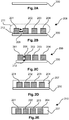
- Figs. 2A to 2E show different intermediate products of the method for fabricating a pixelated scintillator described herein. The figures are shown in a side view.
- connection-structure 200 in this embodiment a base layer 200, which is provided according to the described method, is shown.
- the base layer 200 comprises a second sintering-shrinking-coefficient.
- FIG. 2B the intermediate product after providing the pixelated scintillator-structure 211 is shown.
- the pixelated scintillator-structure 211 is deposited onto the base layer 200 and comprises a plurality of separated pixels 201, 202, 203 and 204.
- the adjacent pixels 201 and 202 are separated by a gap 212 which has a width 205.
- This intermediate product is a pixelated scintillator before sintering 208, wherein the width 205 of the gap 212 separating the two adjacent pixels 201 and 202, for example, amounts to 100 ⁇ m.
- the pixelated scintillator-structure comprises a first sintering-shrinking-coefficient, which is smaller than the second sintering-shrinking-coefficient of the base layer 200.
- a pixelated scintillator after sintering 209 is shown, i.e. an intermediate product of the method described herein.
- the pixels 201, 202, 203 and 204 as well as the base layer 200 have shrunk.
- the base layer 200 has shrunk more than the pixels 201, 202, 203 and 204, such that the width 206 of the gap 212 has shrunk more than the pixels 201, 202, 203 and 204.
- Fig. 2D the intermediate product of the method described herein is shown after the pixels 201, 202, 203 and 204 located on the base layer 200 are coated with a coating material 207, for example, an epoxy reflector.
- a coating material 207 for example, an epoxy reflector.
- Fig. 2E the final pixelated scintillator 210 is shown after the base layer 200 has been removed, for example, has been grinded away.
- the pixelated scintillator-structure comprising the pixels 201, 202, 203 and 204 as well as the coating material 207 remains.
- a pixelated scintillator is shown before and after the sintering step, wherein the pixelated scintillator comprises an interlayer structure 301.
- the pixelated scintillator before sintering comprises a connection-structure 200, in this case a base layer 200 as well as separated pixels, wherein between each pixel 201 and the base layer 200, an interlayer structure 301 is located.
- the base layer 200 is provided first and subsequently the interlayer structure 301 is provided.
- the interlayer structure 301 is provided in such a way that it comprises a plurality of separated interlayer structures 301, which are provided at the positions where the pixel 201 will be provided.
- the interlayer structure 301 may also be provided as a continuous layer, which is located on the base layer 200.
- the pixelated scintillator comprising interlayer structures is shown after the sintering step. Since the interlayer structure 301 has a third sintering-shrinking-coefficient that is smaller than the second sintering-shrinking-coefficient of the base layer 200 and is greater than the first sintering-shrinking-coefficient of the pixel 201 of the pixelated scintillator-structure, the interlayer structure 301 has an intermediate shrinkage. In other words, the interlayer structure 301 shrinks less than the base layer 200 and shrinks more the pixel 201 during the sintering step. In this way, less stresses are caused between the base layer 200 and the pixelated scintillator-structure comprising the pixel 201.
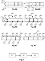
- connection-structure comprises a plurality of separated connection-structures that are located between the pixels of the pixelated scintillator-structure.
- connection-structure comprises separated connection-structures 405, 406, 407 and 408 that are located between the pixels.
- the adjacent pixels 401 and 402 are separated by a gap 410, wherein the connection-structure 405 is located in the gap 410.
- the connection-structure 405 is in mechanical contact with both of the adjacent pixels 401 and 402.
- the connection-structures 406 and 407 are also located in the gap between the two adjacent pixels 402 and 403 or 403 and 404.
- the pixelated scintillator before sintering 208 is shown.
- the connection-structures 405, 406, 407 and 408 may be provided in a way that they do not fill the complete gap. For example, they may only be provided in the lower part of the gap and the pixelated scintillator-structure, respectively.
- Fig. 4B the pixelated scintillator after sintering 209 is shown.
- the pixels 401, 402, 403 and 404 as well as the connection-structures 405, 406, 407 and 408 have shrunk.
- the second sintering-shrinking-coefficient of the connection-structures is greater than the first sintering-shrinking-coefficient of the pixelated scintillator-structure comprising the pixels 401, 402, 403 and 404, the gaps between the pixels have shrunk more than the pixels.
- Fig. 4C the pixelated scintillator fabricated with the method described herein is shown after coating the pixels 401, 402, 403 and 404 and the connection-structures 405, 406, 407 and 408 with a coating material 409, for example with an epoxy reflector.
- Fig. 4D the final pixelated scintillator 210 is shown, in which the lower part of the pixels 401, 402, 403 and 404, where the connection-structures 405, 406, 407 and 408 were located, has been removed, for example, grinded away.
- the pixels 401, 402, 403 and 404 of the pixelated scintillator-structure and the coating material 409 remain.
- the pixelated scintillator is coated with a coating material and that the connection-structure is removed, there may also be pixelated scintillators, where this step is not performed.
- Step S1 of the method relates to the step of providing a pixelated scintillator-structure with a first sintering-shrinking-coefficient, the pixelated scintillator-structure comprising two adjacent pixels which are separated by a gap.
- Step S2 relates to providing a connection structure, which is in mechanical contact with both of the two adjacent pixels, wherein the connection-structure comprises a second sintering-shrinking-coefficient that is greater that the first sintering-shrinking-coefficient.
- step S3 the sintering of the pixelated scintillator-structure and the connection-structure such that the gap is reduced is carried out.
- the steps SI, S2 and S3 are performed subsequently, these steps may also be performed in a different order.
- the step S2 can be performed before the step S1.
- the pixelated scintillator-structure and the connection-structure can be provided in the same method step, for example, with the same print head.
- Fig. 6 shows a pixelated scintillator according to an exemplary embodiment of the invention before sintering 208 and the same pixelated scintillator after sintering 209.
- the pixelated scintillator corresponds to the one described with respect to Figs. 2A to 2E .
- the connection-structure i.e. the base layer
- the connection-structure has a length S p 601
- the pixel has a width P p 602
- the gap between two adjacent pixels has a width G p 603.
- the connection-structure has a length S s 604
- the pixel has a width P s 605
- the gap between two adjacent pixels has a width G s 605.
- the second sintering-shrinking is greater than the first sintering-shrinking coefficient, i.e. the base layer has a greater shrinkage during sintering than the pixelated scintillator-structure.
- the sintering-shrinking-coefficient of the gap is approximately equal to the second sintering-shrinking-coefficient C 2 .
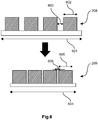
- Fig. 7 shows a detector 700 comprising pixelated scintillator 706 described in the context of the present invention.
- the pixelated scintillator comprises a sintered pixelated scintillator structure comprising at least two adjacent pixels 702 and 703 which are separated by a gap 704.
- the width 705 of the gap 704 is smaller than 150 ⁇ m.
- Fig. 8 shows an imaging apparatus 801 comprising a detector 802 described in the context of the invention, e.g. the detector shown in Fig. 7 .
- the detector 802 comprises a pixelated scintillator 803.
Description
- The invention relates to the field of scintillators. In particular, the invention relates to a method for fabricating a pixelated scintillator.
- Scintillators in radiation detectors may comprise an array of individual pixels which are separated by gaps. Such pixelated scintillators can be formed out of scintillating ceramic material.
- In
US 2012/0308837 A1 a process for the generative preparation of ceramic-shaped bodies by 3D inkjet printing is described. - Document
EP 2 717 272 discloses a method of manufacturing a scintillator panel including a grid-like barrier rib. - It may be desirable to optimize the efficiency of pixelated scintillators. Aspects of the invention are stated in independent claim 1.
- Advantages and further embodiments are set out in the dependent claims, the description and the figures.
- A first aspect of the invention relates to a method for fabricating a pixelated scintillator. The method comprises the step of providing a pixelated scintillator-structure with a first sintering-shrinking-coefficient, the pixelated scintillator-structure comprising two adjacent pixels, both having a top portion and a bottom portion, which are separated by a gap. Furthermore, the method comprises the step of providing a connection-structure, which is in mechanical contact, at the bottom portion of the two adjacent pixels, with both of the two adjacent pixels, wherein the connection-structure comprises a second sintering-shrinking-coefficient that is greater than the first sintering-shrinking coefficient. Moreover, the method comprises the step of sintering the pixelated scintillator-structure and the connection-structure such that the gap is reduced because of the difference between the first and the second sintering-shrinking coefficient.
- A gist of the invention may be seen in providing a method for fabricating a pixelated scintillator with a higher or optimized efficiency. This may be realized by providing two different structures, the scintillator-structure and the connection-structure, which have different sintering-shrinking-coefficients in such a way, that the different sintering-shrinking-coefficients cause that the gap separating two adjacent pixels is reduced during the sintering process.
- The fabrication method may at least partly comprise steps of additive manufacturing, i.e. added layer manufacturing (ALM) and/or 3D printing. For example, the pixelated scintillator-structure and/or the connection-structure may be provided by means of added layer manufacturing and/or 3D printing. The added layer manufacturing and/or 3D printing process may comprise the consecutive deposition of small suspension droplets (inkjet printing) and/or the deposition of thin locally hardened layers. In general, additive manufacturing, i.e. ALM and/or 3D printing, allows the scintillator-structure to be fabricated layer by layer. The provided structures, i.e. the scintillator-structure and/or the connection-structure, may comprise so-called green phase particles in a binder material. These green phase particles in the binder material may form a ceramic scintillator after a heating step which is also referred to as the sintering step. The pixelated scintillator-structure and/or the connection structure may, e.g., be deposited by additive manufacturing. For example, the pixelated scintillator-structure and/or the connection-structure may be deposited on a working surface.
- The scintillator may refer to a device that exhibits scintillation when it is excited by high-energetic photons and/or ionizing radiation, e.g. by X-rays. The pixelated scintillator may comprise a plurality of separated pixels that are configured to be separately and to emit scintillation independently of other pixels of the pixelated scintillator. The pixels of the pixelated scintillator may, for example, have a square-shaped or a circular cross-section. In other words, the pixels of the pixelated scintillator-structure may have a cuboid or cylindrical shape. However, the pixels of the pixelated scintillator-structure may also have a different shape.
- The pixelated scintillator, i.e. the pixelated scintillator-structure and/or the connection-structure, can comprise CsI:Tl, Thallium doped Caesium Iodide, or other ceramic scintillating material. For example, the pixelated scintillator, i.e. the pixelated scintillator-structure and/or the connection-structure can comprise a material selected from the group comprising caesium iodide or zinc sulphide or sodium iodide or lutetium oxyorthosilicate or bismuth germanium oxide or any other scintillating material. Particular, scintillating materials like Gadolinium oxyorthosilicate, known as GSO, may be used, which is a type of scintillating inorganic crystal used for imaging in nuclear medicine and for calorimetry or Lutetium-yttrium oxyorthosilicate, also known as LYSO, which is an inorganic chemical compound with main use as a scintillator crystal.
- Further, for the pixelated scintillator, i.e. the pixelated scintillator-structure and/or the connection-structure, inorganic scintillators may be used, for example, alkali metal halides, often with a small amount of activator impurity, NaI(Tl) (sodium iodide doped with thallium). Other inorganic alkali halide crystals are, for instance: CsI(Tl), CsI(Na), Csl(pure), CsF, KI(Tl), LiI(Eu). Some non-alkali crystals may include: BaF2, CaF2(Eu), ZnS(Ag), CaWO4, CdWO4, YAG(Ce) (Y3A15O12(Ce)). Moreover, for the pixelated scintillator, i.e. the pixelated scintillator-structure and/or the connection-structure, Yttrium aluminium garnet; YAG, Y3A15O12 or any other synthetic crystalline material of the garnet group or of silicate minerals may be used or any intermetallic compound or alloy or any other metallic compounds comprising a rare earth metal, as for instance, Yttrium, Cerium, Terbium, Gallium or Gadolinium.
- The providing of the pixelated scintillator-structure may refer to the step of adding the pixelated scintillator-structure. For example, the pixelated scintillator-structure may be added by additive manufacturing, i.e. ALM and/or 3D printing. Moreover, the pixelated-scintillator structure may be added onto the connection structure, which may be added first.
- In the context of this invention, the term sintering-shrinking-coefficient may refer to a property of the material of the pixelated scintillator-structure and the connection-structure, respectively. The sintering-shrinking-coefficient may refer to the shrinking factor of the respective material during sintering. For example, the sintering-shrinking-coefficient may be expressed in terms of percents. The sintering-shrinking-coefficient may refer to the percentage of the shrinking of a length of a body made out of that material. For example, a sintering-shrinking-coefficient of 20% may refer to the fact that a length of an object shrinks by 20% during sintering. The sintering-shrinking-coefficient of a material may for example be determined by measuring a length of a body made of this material before and after sintering. In this case, the sintering-shrinking-coefficient may be calculated by dividing the difference of the length before sintering and the length after sintering by the length before sintering. For example, the first sintering-shrinking-coefficient of the pixelated scintillator-structure may amount to 20% and the second sintering-shrinking-coefficient of the connection-structure may amount to 40%. However, these are just exemplary values, which may also be different. The sintering-shrinking coefficient of the pixelated scintillator-structure and the connection structure may, for example, be achieved by selecting a specific relative amount of binder material for the pixelated scintillator-structure and the connection-structure.
- Different sintering-shrinking-coefficients may also be achieved by selecting different ceramic materials for the pixelated scintillator-structure and the connection-structure.
- The two adjacent pixels may refer to two pixels of the scintillator-structure which are located next to each other and are separated by a gap. In other words, the gap may be located between the two adjacent pixels. The scintillator-structure may also comprise more than two pixels, wherein each pixel of the plurality of pixels may be separated from an adjacent pixel by a gap.
- The connection-structure may refer to a structure that connects the two adjacent pixels and is in mechanical contact with the two adjacent pixels. There are different ways to realize the connection-structure. For example, the connection-structure may be realized as a base layer, which may, for example, be located underneath the two adjacent pixels. However, the connection-structure may also be located between the two adjacent pixels, i.e. it may be located in the gap separating the two adjacent pixels. Moreover, the connection-structure may also refer to a continuous structure or to a plurality of isolated connection-structures, which are in mechanical contact with both of the two adjacent pixels. The feature that the connection-structure is in mechanical contact with both of the adjacent pixels may refer to the feature that a shrinking of the connection-structure is transferred to the two adjacent pixels such that the gap between the two adjacent pixels is reduced. The reduction of the gap can relate to the reduction of the width of the gap.
- The step of sintering the pixelated scintillator-structure and the connection-structure may refer to a heating step of the scintillator-structure and the connection-structure. For example, sintering is carried out at temperatures between 1600°C and 1800°C. The sintering may be performed at atmospheric pressure. Moreover, during sintering of the pixelated scintillator-structure and the connection-structure it may not be necessary to fix the geometry of said structures such that they may shrink during sintering, i.e. the sintering step may be carried out in such a way that the geometry of the pixelated scintillator-structure and the connection-structure is not fixed.
- The steps of the described method may be carried out in the described order or in another order or even parallel to each other. For example, the providing of the pixelated scintillator-structure may be carried out before, during or after the providing of the connection-structure. Thus, the pixelated scintillator-structure may also be provided at the same time as the connection-structure.
- With this method a pixelated scintillator can be fabricated in such a way that the gap between two adjacent pixels is minimized, i.e. such that the pixelated scintillator comprises a bigger detector surface. In this way, the efficiency of the scintillator is optimized.
- According to an exemplary embodiment, the connection-structure is a base layer, wherein the pixelated scintillator-structure is deposited onto the base layer.
- For example, the base layer is provided first and the pixelated scintillator-structure is deposited in a subsequent step onto the base layer. The base layer may be a continuous layer that is located underneath the pixelated scintillator-structure. Further, the connection-structure may be a base layer and may be deposited on a working surface and the pixelated scintillator-structure may be deposited onto the base layer.
- In this way, the base layer may be provided independently from the pixelated scintillator-structure, i.e. in a separated step of the fabricating method described herein. In other words, the device for providing the base layer and the scintillator-structure can be configured for providing the base layer first and for providing the pixelated scintillator-structure in a subsequent step.
- According to a further exemplary embodiment, the base layer has a thickness between 0.2 mm and 2 mm and the pixelated scintillator-structure has a thickness between 0.2 mm and 5 mm.
- According to a further exemplary embodiment, the method further comprises the step of removing the connection-structure. The connection-structure, e.g. the base layer, may for example be removed by grinding.
- According to a further exemplary embodiment, the method further comprises the step of providing an interlayer-structure comprising a third sintering-shrinking-coefficient, wherein the third sintering-shrinking-coefficient is greater than the first sintering-shrinking-coefficient and smaller than the second sintering-shrinking-coefficient. Furthermore, the interlayer-structure is in mechanical contact with the base layer and the pixelated scintillator-structure. Moreover, the interlayer-structure is sintered together with the base layer and the pixelated scintillator-structure.
- In other words, an interlayer-structure may be provided between the base layer and the pixelated scintillator-structure, wherein the interlayer-structure comprises an intermediate sintering-shrinking-coefficient, such that stresses between the base layer and the pixelated scintillator-structure, which may be due to the different sintering-shrinking-coefficients, can be reduced. In this way, a warpage of the scintillator can be avoided or at least reduced. Moreover, the interlayer-structure can itself comprise a plurality of different layers with different sintering-shrinking-coefficients such that the interlayer has a gradient of sintering-shrinking-coefficients. Moreover, the interlayer-structure may also be provided as a continuous layer that is deposited onto the base layer. It is also possible to provide the interlayer-structure as separated interlayer-structures which are located between the base layer and each pixel, i.e. such that each pixel comprises an interlayer structure located between the pixel and the base layer.
- According to a further exemplary embodiment, the connection-structure is provided in the gap separating the two adjacent pixels. The connection-structure may for example continuously fill the gap separating the two adjacent pixels or be provided as isolated dots in the gap separating the two adjacent pixels.
- In other words, the connection-structure may be provided between the scintillator pixels, for example at the bottom part of the pixelated scintillator-structure. By providing the connection-structure as isolated dots between the pixels, i.e. not as a continuous structure, the warpage of the pixelated scintillator-structure may be further reduced or avoided. Moreover, the connection-structure may only be located on one end of the gap, e.g. on the lower end. After sintering the portion of the pixelated scintillator-structure comprising the connection-structure in the gap separating the two adjacent pixels, e.g. the lower end, can be removed, for example by grinding.
- According to a further exemplary embodiment, the providing of the pixelated scintillator-structure is done by additive layer manufacturing. Moreover, also the providing of the connection-structure and/or the interlayer structure may be done by additive layer manufacturing.
- In the context of the invention, the additive layer manufacturing may also refer to 3D printing, this may be carried out by consecutive deposition of small suspension droplets (inkjet printing) or by consecutive deposition of thin locally hardened layers. According to a further exemplary embodiment, the pixels of the provided pixelated scintillator-structure have a width between 0.05 mm and 2 mm and the gap of the provided pixelated scintillator-structure has a width below 150 µm after sintering. Preferably, the width of the gaps of the provided pixelated scintillator-structure may have a width below 100 µm, more preferable below 50 µm, even more preferable below 10 µm, after sintering.
- According to a further exemplary embodiment, the ratio between the first sintering-shrinking-coefficient and the second sintering-shrinking-coefficient is between 0.95 and 0.2. For example, the pixelated scintillator-structure may comprise a first sintering-shrinking-coefficient amounting to 20% and the connection-structure may comprise a second sintering-shrinking-coefficient amounting to 40%.
- With such a ratio of the first and second sintering-shrinking-coefficients, the shrinkage of the gap is stronger than the shrinkage of the pixel such that the scintillator surface and the efficiency of the scintillator are enhanced.
- According to a further exemplary embodiment, the provided scintillator-structure comprises a scintillating ceramic material with a first relative amount of binding material. The provided connection-structure comprises the scintillating ceramic material with a second relative amount of binding material. Hereby, the first relative amount of binding material and the second relative amount of binding material are different.
- The relative amount of binding material may refer to the particle concentration of binding material in the scintillator-structure and the connection-structure, respectively. The difference between the first relative amount of binding material and the second relative amount of binding material may cause that the first sintering-shrinking-coefficient is different than the second sintering-shrinking-coefficient.
- According to another exemplary embodiment, the method further comprises the step of coating the pixelated scintillator-structure with a reflective coating material. By coating the pixelated scintillator-structure the gaps separating the pixels may be filled with a light-reflective material.
- For example, the pixelated scintillator-structure may be coated with a light-reflective material, e.g. an epoxy material with reflective, e.g. white, particles. The epoxy material may be a TiO2-filled epoxy reflector. Alternatively, thin reflective layers of Al or Ag can be applied to the pixelated scintillator-structure.
- Another aspect relates to a pixelated scintillator comprising: a pixelated scintillator-structure with a first sintering-shrinking-coefficient, the pixelated scintillator-structure comprising two adjacent pixels which are separated by a gap. The pixelated scintillator furthermore comprises a connection-structure, which is in mechanical contact with both of the two adjacent pixels, wherein the connection-structure comprises a second sintering-shrinking-coefficient that is greater than the first sintering-shrinking coefficient.
- The features of the pixelated scintillator described with respect to the method described herein may also describe or define the pixelated scintillator. The pixelated scintillator may, e.g., be an intermediate product of the method described herein. For example, the pixelated scintillator may emerge before the sintering process. This pixelated scintillator may have the property that the gap is reduced more than the pixels such after sintering the pixelated scintillator such that the scintillator surface and the efficiency of the scintillator are maximized.
- A further aspect relates to a pixelated scintillator comprising a pixelated scintillator-structure comprising two adjacent pixels which are separated by a gap (212), wherein the gap has a width below 150 µm. Preferably, the width of the gaps of the pixelated scintillator-structure may have a width below 100 µm, more preferable below 50 µm, even more preferable below 10 µm.
- The pixelated scintillator may be fabricated with a method described in the context of the present invention. Thus, the pixelated scintillator may relate to a final product of the method described herein. For example, the pixelated scintillator is fabricated by added layer manufacturing, e.g. ALM and/or 3D printing. Moreover, the pixelated scintillator structure may be sintered as described with respect to the described method. The pixelated scintillator may comprise materials used in the described fabrication method. Thus, the pixelated scintillator structure may comprise a scintillating ceramic material, e.g., CsI:Tl, Thallium doped Caesium Iodide or any other ceramic scintillating material described herein.
- According to an exemplary embodiment, wherein the pixels of the pixelated scintillator-structure have a width between 0.05 mm and 2 mm. Furthermore, the pixelated scintillator-structure has a thickness between 0.2 mm and 5 mm.
- A further aspect of the invention relates to a detector comprising a pixelated scintillator. The detector may be a radiation detector, e.g. an X-ray detector.
- A further aspect relates to an imaging apparatus comprising a detector.
- The imaging apparatus may be a medical imaging apparatus, e.g. an X-ray imaging apparatus.
- These and other aspects of the invention will be apparent from and elucidated with reference to the embodiments described hereinafter.
-
Fig. 1 shows a pixelated scintillator according to an exemplary embodiment. -
Figs. 2A to 2E show different fabrication steps of a pixelated scintillator according to exemplary embodiments of the invention. -
Figs. 3A and 3B show a pixelated scintillator with an interlayer before and after sintering according to exemplary embodiments of the invention. -
Figs. 4A to 4D show different fabrication steps of a pixelated scintillator according to exemplary embodiments of the invention. -
Fig. 5 shows a flow-chart of a method according to an exemplary embodiment of the invention. -
Fig. 6 shows a pixelated scintillator according to an exemplary embodiment of the invention before and after sintering. -
Fig. 7 shows a detector according to an exemplary embodiment. -
Fig. 8 shows an imaging apparatus according to an exemplary embodiment - The figures are schematic and not true to scale. If the same reference signs are used in different figures, they may refer to identical or similar elements. However, similar or identical elements may also be labelled with different reference signs.
- For the sake of clarity, pixelated scintillators with a small number of pixels are shown in the exemplary embodiments. However, the pixelated scintillator may also have a greater number of pixels, e.g. 16 x 16 pixels, or another number of pixels.
-
Fig. 1 shows apixelated scintillator 100 according to an exemplary embodiment of the invention. Thepixelated scintillator 100 comprises a pixelated scintillator-structure 106 with a first sintering-shrinking-coefficient, the pixelated scintillator-structure 106 comprising twoadjacent pixels gap 104. Furthermore, thepixelated scintillator 100 comprises a connection-structure 101, which is in mechanical contact, only at the base of the two adjacent pixels, with both of the twoadjacent pixels structure 101 comprises a second sintering-shrinking-coefficient that is greater than the first sintering-shrinking-coefficient. The sintering-shrinking coefficients are, e.g., explained with reference toFig. 6 . - In this exemplary embodiment, the connection-
structure 101 is a base layer, on which the pixelated scintillator-structure 106 is provided. Thebase layer 101 is for example also provided by additive manufacturing and/or 3D printing and is formed as a continuous planar layer. - The
pixelated scintillator 100 according to this exemplary embodiment is an intermediate product of the method described herein and is shown before the sintering step. Before the sintering, thegap 104 separating the twoadjacent pixels width 105, which, for example, amounts to 100 µm or more. After sintering, thewidth 105 of thegap 104 will be less than 50 µm. -
Figs. 2A to 2E show different intermediate products of the method for fabricating a pixelated scintillator described herein. The figures are shown in a side view. - In
Fig. 2A , a connection-structure 200, in this embodiment abase layer 200, which is provided according to the described method, is shown. Thebase layer 200 comprises a second sintering-shrinking-coefficient. - In
Fig. 2B , the intermediate product after providing the pixelated scintillator-structure 211 is shown. The pixelated scintillator-structure 211 is deposited onto thebase layer 200 and comprises a plurality ofseparated pixels adjacent pixels gap 212 which has awidth 205. This intermediate product is a pixelated scintillator before sintering 208, wherein thewidth 205 of thegap 212 separating the twoadjacent pixels base layer 200. - In
Fig. 2C , a pixelated scintillator after sintering 209 is shown, i.e. an intermediate product of the method described herein. During the sintering step thepixels base layer 200 have shrunk. However, due to the greater second sintering-shrinking-coefficient of thebase layer 200, thebase layer 200 has shrunk more than thepixels width 206 of thegap 212 has shrunk more than thepixels - In
Fig. 2D , the intermediate product of the method described herein is shown after thepixels base layer 200 are coated with acoating material 207, for example, an epoxy reflector. - In
Fig. 2E , the finalpixelated scintillator 210 is shown after thebase layer 200 has been removed, for example, has been grinded away. Thus, only the pixelated scintillator-structure comprising thepixels coating material 207 remains. - In
Figs. 3A and 3B , a pixelated scintillator is shown before and after the sintering step, wherein the pixelated scintillator comprises aninterlayer structure 301. InFig. 3A it is shown that the pixelated scintillator before sintering comprises a connection-structure 200, in this case abase layer 200 as well as separated pixels, wherein between eachpixel 201 and thebase layer 200, aninterlayer structure 301 is located. According to this exemplary embodiment, thebase layer 200 is provided first and subsequently theinterlayer structure 301 is provided. Theinterlayer structure 301 is provided in such a way that it comprises a plurality of separatedinterlayer structures 301, which are provided at the positions where thepixel 201 will be provided. However, theinterlayer structure 301 may also be provided as a continuous layer, which is located on thebase layer 200. - In
Fig. 3B , the pixelated scintillator comprising interlayer structures is shown after the sintering step. Since theinterlayer structure 301 has a third sintering-shrinking-coefficient that is smaller than the second sintering-shrinking-coefficient of thebase layer 200 and is greater than the first sintering-shrinking-coefficient of thepixel 201 of the pixelated scintillator-structure, theinterlayer structure 301 has an intermediate shrinkage. In other words, theinterlayer structure 301 shrinks less than thebase layer 200 and shrinks more thepixel 201 during the sintering step. In this way, less stresses are caused between thebase layer 200 and the pixelated scintillator-structure comprising thepixel 201. - In
Figs. 4A to 4D , intermediate products of a method described herein are shown, wherein the connection-structure comprises a plurality of separated connection-structures that are located between the pixels of the pixelated scintillator-structure. - In
Fig. 4A it is shown that a plurality ofpixels structures adjacent pixels gap 410, wherein the connection-structure 405 is located in thegap 410. In this way, the connection-structure 405 is in mechanical contact with both of theadjacent pixels structures adjacent pixels Fig. 4A , the pixelated scintillator before sintering 208 is shown. The connection-structures - In
Fig. 4B , the pixelated scintillator after sintering 209 is shown. During sintering, thepixels structures pixels - In
Fig. 4C , the pixelated scintillator fabricated with the method described herein is shown after coating thepixels structures coating material 409, for example with an epoxy reflector. InFig. 4D , the finalpixelated scintillator 210 is shown, in which the lower part of thepixels structures pixels coating material 409 remain. - Although it is shown in exemplary embodiments that the pixelated scintillator is coated with a coating material and that the connection-structure is removed, there may also be pixelated scintillators, where this step is not performed.
- In
Fig. 5 , a flow-chart for a method for fabricating a pixelated scintillator according to an exemplary embodiment of the invention is shown. Step S1 of the method relates to the step of providing a pixelated scintillator-structure with a first sintering-shrinking-coefficient, the pixelated scintillator-structure comprising two adjacent pixels which are separated by a gap. Step S2 relates to providing a connection structure, which is in mechanical contact with both of the two adjacent pixels, wherein the connection-structure comprises a second sintering-shrinking-coefficient that is greater that the first sintering-shrinking-coefficient. In step S3, the sintering of the pixelated scintillator-structure and the connection-structure such that the gap is reduced is carried out. - Although it is shown that the steps SI, S2 and S3 are performed subsequently, these steps may also be performed in a different order. For example, the step S2 can be performed before the step S1. Moreover, it is possible to carry out the steps S1 and S2 at the same time. For example, when providing the connection-structure between two adjacent pixels as shown in
Figs. 4A to 4D , the pixelated scintillator-structure and the connection-structure can be provided in the same method step, for example, with the same print head. -
Fig. 6 shows a pixelated scintillator according to an exemplary embodiment of the invention before sintering 208 and the same pixelated scintillator after sintering 209. The pixelated scintillator, for example, corresponds to the one described with respect toFigs. 2A to 2E . Before sintering, the connection-structure, i.e. the base layer, has alength S p 601, the pixel has awidth P p 602, and the gap between two adjacent pixels has awidth G p 603. After sintering, the connection-structure has alength S s 604, the pixel has awidth P s 605, and the gap between two adjacent pixels has awidth G s 605. The first sintering-shrinking-coefficient C1 of the pixelated scintillator-structure can be calculated as

- As explained before, the second sintering-shrinking is greater than the first sintering-shrinking coefficient, i.e. the base layer has a greater shrinkage during sintering than the pixelated scintillator-structure. The sintering-shrinking-coefficient of the gap is approximately equal to the second sintering-shrinking-coefficient C2.
-
Fig. 7 shows adetector 700 comprisingpixelated scintillator 706 described in the context of the present invention. The pixelated scintillator comprises a sintered pixelated scintillator structure comprising at least twoadjacent pixels gap 704. Thewidth 705 of thegap 704 is smaller than 150 µm. -
Fig. 8 shows animaging apparatus 801 comprising adetector 802 described in the context of the invention, e.g. the detector shown inFig. 7 . Thedetector 802 comprises apixelated scintillator 803. - Other variations to the disclosed embodiments can be understood and effected by those skilled in the art in practising the claimed invention, from a study of the drawings, the disclosure, and the appended claims. In the claims, the word "comprising" does not exclude other elements or steps, and the indefinite article "a" or "an" does not exclude a plurality. The mere fact that certain measures are recited in mutually different dependent claims does not indicate that a combination of these measures cannot be used to advantage. Any reference signs in the claims should not be construed as limiting the scope.
Claims (11)
- Method for fabricating a pixelated scintillator (100), the method comprising the steps:providing a pixelated scintillator-structure (211) with a first sintering-shrinking-coefficient, the pixelated scintillator-structure comprising two adjacent pixels (201, 202), both having a top portion and a bottom portion, which are separated by a gap (212) (S1);providing a connection-structure (200, 405), which is in mechanical contact, at the bottom portion of the two adjacent pixels, with both of the two adjacent pixels, wherein the connection-structure comprises a second sintering-shrinking-coefficient that is greater than the first sintering-shrinking coefficient (S2); andsintering (S3) the pixelated scintillator-structure (211) and the connection-structure (200, 405).
- Method according to claim 1,
wherein the connection-structure is a base layer (200); and
wherein the pixelated scintillator-structure (211) is deposited onto the base layer (200). - Method according claim 2,
wherein the base layer (200) has a thickness between 0.2 mm and 2 mm; and
wherein the pixelated scintillator-structure (211) has a thickness between 0.2 mm and 5 mm. - Method according to any one of claims 2 and 3, further comprising the step:providing an interlayer structure (301) comprising a third sintering-shrinking-coefficient, wherein the third sintering-shrinking-coefficient is smaller than the second sintering-shrinking-coefficient and is greater than the first sintering-shrinking-coefficient, the interlayer material being in mechanical contact with the base layer (200) and the pixelated scintillator-structure (211); andwherein the interlayer material is sintered together with the base layer and the pixelated scintillator-structure.
- Method according to any one of the preceding claims, further comprising the step:
removing the connection-structure (200). - Method according to any one of the preceding claims,
wherein the connection-structure (405) is provided in the gap (410) separating the two adjacent pixels (401, 402). - Method according to any one of the preceding claims,
wherein the providing of the pixelated scintillator-structure (211) is done by additive layer manufacturing. - Method according to any one of the preceding claims,
wherein the pixels (201, 202, 203, 204) of the provided pixelated scintillator-structure (211) have a width between 0.05 mm and 2 mm and the gap of the provided pixelated scintillator-structure has a width below 150 µm after sintering. - Method according to any one of the preceding claims,
wherein the ratio between the first sintering-shrinking-coefficient and the second sintering-shrinking-coefficient is between 0.95 and 0.2. - Method according to any one of the preceding claims,
wherein the provided scintillator-structure (211) comprises a scintillating ceramic material with a first relative amount of binding material;
wherein the provided connection-structure (200, 405) comprises the scintillating ceramic material with a second relative amount of binding material; and
wherein the first relative amount and the second relative amount are different. - Method according to any one of the preceding claims, further comprising the step:
coating the pixelated scintillator-structure (211) with a reflective coating material.
Applications Claiming Priority (2)
| Application Number | Priority Date | Filing Date | Title |
|---|---|---|---|
| EP14193004 | 2014-11-13 | ||
| PCT/EP2015/075193 WO2016074945A1 (en) | 2014-11-13 | 2015-10-30 | Pixelated scintillator with optimized efficiency |
Publications (2)
| Publication Number | Publication Date |
|---|---|
| EP3218932A1 EP3218932A1 (en) | 2017-09-20 |
| EP3218932B1 true EP3218932B1 (en) | 2018-10-24 |
Family
ID=51893912
Family Applications (1)
| Application Number | Title | Priority Date | Filing Date |
|---|---|---|---|
| EP15790085.3A Active EP3218932B1 (en) | 2014-11-13 | 2015-10-30 | Method of fabricating a pixelated scintillator with optimized efficiency |
Country Status (5)
| Country | Link |
|---|---|
| US (1) | US9989652B2 (en) |
| EP (1) | EP3218932B1 (en) |
| JP (1) | JP6356352B2 (en) |
| CN (1) | CN107004686B (en) |
| WO (1) | WO2016074945A1 (en) |
Families Citing this family (4)
| Publication number | Priority date | Publication date | Assignee | Title |
|---|---|---|---|---|
| EP3495849A1 (en) * | 2017-12-11 | 2019-06-12 | Koninklijke Philips N.V. | Multilayer pixelated scintillator with enlarged fill factor |
| EP3499272A1 (en) * | 2017-12-14 | 2019-06-19 | Koninklijke Philips N.V. | Structured surface part for radiation capturing devices, method of manufacturing such a part and x-ray detector |
| EP3553568A1 (en) * | 2018-04-12 | 2019-10-16 | Koninklijke Philips N.V. | X-ray detector with focused scintillator structure for uniform imaging |
| EP3620826A1 (en) | 2018-09-10 | 2020-03-11 | Koninklijke Philips N.V. | Multi-piece mono-layer radiation detector |
Family Cites Families (18)
| Publication number | Priority date | Publication date | Assignee | Title |
|---|---|---|---|---|
| US5598056A (en) | 1995-01-31 | 1997-01-28 | Lucent Technologies Inc. | Multilayer pillar structure for improved field emission devices |
| US6361735B1 (en) * | 1999-09-01 | 2002-03-26 | General Electric Company | Composite ceramic article and method of making |
| JP2001099941A (en) * | 1999-09-30 | 2001-04-13 | Hitachi Metals Ltd | Radiation shielding plate, radiation detector, and manufacturing method of radiation shielding plate |
| US6921909B2 (en) * | 2002-08-27 | 2005-07-26 | Radiation Monitoring Devices, Inc. | Pixellated micro-columnar films scintillator |
| DE10242006B4 (en) * | 2002-09-11 | 2006-04-27 | Siemens Ag | Phosphor plate |
| DE102004043273A1 (en) | 2003-09-09 | 2005-05-04 | Ngk Spark Plug Co | Process for producing a ceramic substrate and ceramic substrate |
| JP2005300190A (en) * | 2004-04-07 | 2005-10-27 | Konica Minolta Holdings Inc | Phosphor coating, method for manufacturing the same and radiographic image conversion panel using the same |
| DE102004056999A1 (en) * | 2004-11-25 | 2006-06-01 | Siemens Ag | Making scintillator layer for x-ray detector with spatial resolution, introduces fluorescing polymer mixture into pattern of holes and hardens it |
| JP2009189801A (en) * | 2008-01-18 | 2009-08-27 | Toshiba Corp | Radiation detector, x-ray ct apparatus, and method for manufacturing radiation detector |
| US20100127180A1 (en) * | 2008-11-24 | 2010-05-27 | Cmt Medical Technologies Ltd. | Scintillator array and a method of constructing the same |
| US9177683B2 (en) | 2011-05-26 | 2015-11-03 | Toray Industries, Inc. | Scintillator panel and method for manufacturing scintillator panel |
| EP2529694B1 (en) | 2011-05-31 | 2017-11-15 | Ivoclar Vivadent AG | Method for generative production of ceramic forms by means of 3D jet printing |
| CN103842848B (en) | 2011-08-30 | 2016-03-30 | 圣戈本陶瓷及塑料股份有限公司 | For system, the method and apparatus of deep trouth shallow cut pixelation |
| JP2013115325A (en) | 2011-11-30 | 2013-06-10 | Kyocera Corp | Manufacturing method of sintered structure |
| JPWO2014021415A1 (en) | 2012-08-03 | 2016-07-21 | 東レ株式会社 | Scintillator panel and method for manufacturing scintillator panel |
| US9886526B2 (en) | 2012-10-11 | 2018-02-06 | University Of Southern California | 3D printing shrinkage compensation using radial and angular layer perimeter point information |
| CN203838347U (en) * | 2014-04-25 | 2014-09-17 | 中国科学院宁波材料技术与工程研究所 | Scintillator array preparation mould |
| WO2016006484A1 (en) * | 2014-07-08 | 2016-01-14 | 東レ株式会社 | Large-building inspection device |
-
2015
- 2015-10-30 US US15/524,696 patent/US9989652B2/en active Active
- 2015-10-30 CN CN201580061634.0A patent/CN107004686B/en active Active
- 2015-10-30 WO PCT/EP2015/075193 patent/WO2016074945A1/en active Application Filing
- 2015-10-30 EP EP15790085.3A patent/EP3218932B1/en active Active
- 2015-10-30 JP JP2017525905A patent/JP6356352B2/en not_active Expired - Fee Related
Non-Patent Citations (1)
| Title |
|---|
| None * |
Also Published As
| Publication number | Publication date |
|---|---|
| JP6356352B2 (en) | 2018-07-11 |
| JP2018500549A (en) | 2018-01-11 |
| CN107004686B (en) | 2021-07-20 |
| US9989652B2 (en) | 2018-06-05 |
| CN107004686A (en) | 2017-08-01 |
| EP3218932A1 (en) | 2017-09-20 |
| WO2016074945A1 (en) | 2016-05-19 |
| US20170322320A1 (en) | 2017-11-09 |
Similar Documents
| Publication | Publication Date | Title |
|---|---|---|
| EP3218932B1 (en) | Method of fabricating a pixelated scintillator with optimized efficiency | |
| Van Eijk | Inorganic scintillators in medical imaging | |
| JP6113662B2 (en) | Scintillator array and X-ray detector and X-ray inspection apparatus using the same | |
| US9121952B2 (en) | Scintillators and applications thereof | |
| EP2739991B1 (en) | Scintillator having a phase separation structure and radiation detector using the same | |
| EP2141708A1 (en) | Scintillator panel and radiation detector | |
| EP1995608A1 (en) | Radiation detector and method for producing the same | |
| CN106947480B (en) | Ceramic phosphor laminates with fused optical elements, methods of making the same, and articles comprising the same | |
| EP3132286B1 (en) | Radiation detector with photosensitive elements that can have high aspect ratios | |
| US10345456B2 (en) | Radiation detector and method for producing a radiation detector | |
| CN109991648A (en) | A method of making scintillator arrays | |
| KR20170066234A (en) | Method of manufacturing garnet interfaces and articles containing the garnets obtained therefrom | |
| EP3392678B1 (en) | Scintillator panel and radiation detector | |
| EP1051643B1 (en) | Method of manufacturing a layered scintillation detector | |
| CN211505908U (en) | Scintillator with multistage light intensity adjustment | |
| JP5767765B2 (en) | High resolution phosphor screen and method for producing high resolution phosphor screen | |
| JP6460440B2 (en) | X-ray phosphor plate | |
| CN110967723A (en) | Scintillator with multistage light intensity adjustment | |
| US11958785B2 (en) | Bonding scintillator material to produce large panels or other shapes | |
| JP2018096714A (en) | Scintillator plate, radiation detector and radiation measurement system | |
| KR20210081146A (en) | Curved Radiation Detector for Implementing Low Dose and High Resolution using Backside Light-Receiving Structure | |
| WO2021096585A1 (en) | Bonding scintillator material to produce large panels or other shapes | |
| CN111410563A (en) | Metallized isolated scintillating ceramic array structure and preparation method thereof |
Legal Events
| Date | Code | Title | Description |
|---|---|---|---|
| PUAI | Public reference made under article 153(3) epc to a published international application that has entered the european phase |
Free format text: ORIGINAL CODE: 0009012 |
|
| 17P | Request for examination filed |
Effective date: 20170613 |
|
| AK | Designated contracting states |
Kind code of ref document: A1 Designated state(s): AL AT BE BG CH CY CZ DE DK EE ES FI FR GB GR HR HU IE IS IT LI LT LU LV MC MK MT NL NO PL PT RO RS SE SI SK SM TR |
|
| AX | Request for extension of the european patent |
Extension state: BA ME |
|
| DAV | Request for validation of the european patent (deleted) | ||
| DAX | Request for extension of the european patent (deleted) | ||
| RIC1 | Information provided on ipc code assigned before grant |
Ipc: G01T 1/20 20060101ALI20180329BHEP Ipc: G01T 1/24 20060101ALI20180329BHEP Ipc: H01L 27/146 20060101AFI20180329BHEP |
|
| GRAP | Despatch of communication of intention to grant a patent |
Free format text: ORIGINAL CODE: EPIDOSNIGR1 |
|
| INTG | Intention to grant announced |
Effective date: 20180508 |
|
| GRAS | Grant fee paid |
Free format text: ORIGINAL CODE: EPIDOSNIGR3 |
|
| GRAA | (expected) grant |
Free format text: ORIGINAL CODE: 0009210 |
|
| AK | Designated contracting states |
Kind code of ref document: B1 Designated state(s): AL AT BE BG CH CY CZ DE DK EE ES FI FR GB GR HR HU IE IS IT LI LT LU LV MC MK MT NL NO PL PT RO RS SE SI SK SM TR |
|
| REG | Reference to a national code |
Ref country code: FR Ref legal event code: PLFP Year of fee payment: 4 |
|
| REG | Reference to a national code |
Ref country code: CH Ref legal event code: EP |
|
| REG | Reference to a national code |
Ref country code: IE Ref legal event code: FG4D |
|
| REG | Reference to a national code |
Ref country code: AT Ref legal event code: REF Ref document number: 1057697 Country of ref document: AT Kind code of ref document: T Effective date: 20181115 |
|
| REG | Reference to a national code |
Ref country code: DE Ref legal event code: R096 Ref document number: 602015018806 Country of ref document: DE |
|
| REG | Reference to a national code |
Ref country code: NL Ref legal event code: MP Effective date: 20181024 |
|
| REG | Reference to a national code |
Ref country code: LT Ref legal event code: MG4D |
|
| REG | Reference to a national code |
Ref country code: AT Ref legal event code: MK05 Ref document number: 1057697 Country of ref document: AT Kind code of ref document: T Effective date: 20181024 |
|
| PG25 | Lapsed in a contracting state [announced via postgrant information from national office to epo] |
Ref country code: NL Free format text: LAPSE BECAUSE OF FAILURE TO SUBMIT A TRANSLATION OF THE DESCRIPTION OR TO PAY THE FEE WITHIN THE PRESCRIBED TIME-LIMIT Effective date: 20181024 |
|
| PG25 | Lapsed in a contracting state [announced via postgrant information from national office to epo] |
Ref country code: ES Free format text: LAPSE BECAUSE OF FAILURE TO SUBMIT A TRANSLATION OF THE DESCRIPTION OR TO PAY THE FEE WITHIN THE PRESCRIBED TIME-LIMIT Effective date: 20181024 Ref country code: IS Free format text: LAPSE BECAUSE OF FAILURE TO SUBMIT A TRANSLATION OF THE DESCRIPTION OR TO PAY THE FEE WITHIN THE PRESCRIBED TIME-LIMIT Effective date: 20190224 Ref country code: AT Free format text: LAPSE BECAUSE OF FAILURE TO SUBMIT A TRANSLATION OF THE DESCRIPTION OR TO PAY THE FEE WITHIN THE PRESCRIBED TIME-LIMIT Effective date: 20181024 Ref country code: HR Free format text: LAPSE BECAUSE OF FAILURE TO SUBMIT A TRANSLATION OF THE DESCRIPTION OR TO PAY THE FEE WITHIN THE PRESCRIBED TIME-LIMIT Effective date: 20181024 Ref country code: NO Free format text: LAPSE BECAUSE OF FAILURE TO SUBMIT A TRANSLATION OF THE DESCRIPTION OR TO PAY THE FEE WITHIN THE PRESCRIBED TIME-LIMIT Effective date: 20190124 Ref country code: PL Free format text: LAPSE BECAUSE OF FAILURE TO SUBMIT A TRANSLATION OF THE DESCRIPTION OR TO PAY THE FEE WITHIN THE PRESCRIBED TIME-LIMIT Effective date: 20181024 Ref country code: BG Free format text: LAPSE BECAUSE OF FAILURE TO SUBMIT A TRANSLATION OF THE DESCRIPTION OR TO PAY THE FEE WITHIN THE PRESCRIBED TIME-LIMIT Effective date: 20190124 Ref country code: LT Free format text: LAPSE BECAUSE OF FAILURE TO SUBMIT A TRANSLATION OF THE DESCRIPTION OR TO PAY THE FEE WITHIN THE PRESCRIBED TIME-LIMIT Effective date: 20181024 Ref country code: FI Free format text: LAPSE BECAUSE OF FAILURE TO SUBMIT A TRANSLATION OF THE DESCRIPTION OR TO PAY THE FEE WITHIN THE PRESCRIBED TIME-LIMIT Effective date: 20181024 Ref country code: LV Free format text: LAPSE BECAUSE OF FAILURE TO SUBMIT A TRANSLATION OF THE DESCRIPTION OR TO PAY THE FEE WITHIN THE PRESCRIBED TIME-LIMIT Effective date: 20181024 |
|
| PG25 | Lapsed in a contracting state [announced via postgrant information from national office to epo] |
Ref country code: AL Free format text: LAPSE BECAUSE OF FAILURE TO SUBMIT A TRANSLATION OF THE DESCRIPTION OR TO PAY THE FEE WITHIN THE PRESCRIBED TIME-LIMIT Effective date: 20181024 Ref country code: SE Free format text: LAPSE BECAUSE OF FAILURE TO SUBMIT A TRANSLATION OF THE DESCRIPTION OR TO PAY THE FEE WITHIN THE PRESCRIBED TIME-LIMIT Effective date: 20181024 Ref country code: RS Free format text: LAPSE BECAUSE OF FAILURE TO SUBMIT A TRANSLATION OF THE DESCRIPTION OR TO PAY THE FEE WITHIN THE PRESCRIBED TIME-LIMIT Effective date: 20181024 Ref country code: PT Free format text: LAPSE BECAUSE OF FAILURE TO SUBMIT A TRANSLATION OF THE DESCRIPTION OR TO PAY THE FEE WITHIN THE PRESCRIBED TIME-LIMIT Effective date: 20190224 Ref country code: GR Free format text: LAPSE BECAUSE OF FAILURE TO SUBMIT A TRANSLATION OF THE DESCRIPTION OR TO PAY THE FEE WITHIN THE PRESCRIBED TIME-LIMIT Effective date: 20190125 |
|
| REG | Reference to a national code |
Ref country code: CH Ref legal event code: PL |
|
| REG | Reference to a national code |
Ref country code: BE Ref legal event code: MM Effective date: 20181031 |
|
| PG25 | Lapsed in a contracting state [announced via postgrant information from national office to epo] |
Ref country code: LU Free format text: LAPSE BECAUSE OF NON-PAYMENT OF DUE FEES Effective date: 20181030 |
|
| REG | Reference to a national code |
Ref country code: IE Ref legal event code: MM4A |
|
| REG | Reference to a national code |
Ref country code: DE Ref legal event code: R097 Ref document number: 602015018806 Country of ref document: DE |
|
| PG25 | Lapsed in a contracting state [announced via postgrant information from national office to epo] |
Ref country code: CZ Free format text: LAPSE BECAUSE OF FAILURE TO SUBMIT A TRANSLATION OF THE DESCRIPTION OR TO PAY THE FEE WITHIN THE PRESCRIBED TIME-LIMIT Effective date: 20181024 Ref country code: DK Free format text: LAPSE BECAUSE OF FAILURE TO SUBMIT A TRANSLATION OF THE DESCRIPTION OR TO PAY THE FEE WITHIN THE PRESCRIBED TIME-LIMIT Effective date: 20181024 Ref country code: IT Free format text: LAPSE BECAUSE OF FAILURE TO SUBMIT A TRANSLATION OF THE DESCRIPTION OR TO PAY THE FEE WITHIN THE PRESCRIBED TIME-LIMIT Effective date: 20181024 |
|
| PG25 | Lapsed in a contracting state [announced via postgrant information from national office to epo] |
Ref country code: LI Free format text: LAPSE BECAUSE OF NON-PAYMENT OF DUE FEES Effective date: 20181031 Ref country code: EE Free format text: LAPSE BECAUSE OF FAILURE TO SUBMIT A TRANSLATION OF THE DESCRIPTION OR TO PAY THE FEE WITHIN THE PRESCRIBED TIME-LIMIT Effective date: 20181024 Ref country code: SM Free format text: LAPSE BECAUSE OF FAILURE TO SUBMIT A TRANSLATION OF THE DESCRIPTION OR TO PAY THE FEE WITHIN THE PRESCRIBED TIME-LIMIT Effective date: 20181024 Ref country code: RO Free format text: LAPSE BECAUSE OF FAILURE TO SUBMIT A TRANSLATION OF THE DESCRIPTION OR TO PAY THE FEE WITHIN THE PRESCRIBED TIME-LIMIT Effective date: 20181024 Ref country code: BE Free format text: LAPSE BECAUSE OF NON-PAYMENT OF DUE FEES Effective date: 20181031 Ref country code: CH Free format text: LAPSE BECAUSE OF NON-PAYMENT OF DUE FEES Effective date: 20181031 Ref country code: SK Free format text: LAPSE BECAUSE OF FAILURE TO SUBMIT A TRANSLATION OF THE DESCRIPTION OR TO PAY THE FEE WITHIN THE PRESCRIBED TIME-LIMIT Effective date: 20181024 Ref country code: MC Free format text: LAPSE BECAUSE OF FAILURE TO SUBMIT A TRANSLATION OF THE DESCRIPTION OR TO PAY THE FEE WITHIN THE PRESCRIBED TIME-LIMIT Effective date: 20181024 |
|
| PLBE | No opposition filed within time limit |
Free format text: ORIGINAL CODE: 0009261 |
|
| STAA | Information on the status of an ep patent application or granted ep patent |
Free format text: STATUS: NO OPPOSITION FILED WITHIN TIME LIMIT |
|
| 26N | No opposition filed |
Effective date: 20190725 |
|
| PG25 | Lapsed in a contracting state [announced via postgrant information from national office to epo] |
Ref country code: IE Free format text: LAPSE BECAUSE OF NON-PAYMENT OF DUE FEES Effective date: 20181030 Ref country code: SI Free format text: LAPSE BECAUSE OF FAILURE TO SUBMIT A TRANSLATION OF THE DESCRIPTION OR TO PAY THE FEE WITHIN THE PRESCRIBED TIME-LIMIT Effective date: 20181024 |
|
| PG25 | Lapsed in a contracting state [announced via postgrant information from national office to epo] |
Ref country code: MT Free format text: LAPSE BECAUSE OF NON-PAYMENT OF DUE FEES Effective date: 20181030 |
|
| PG25 | Lapsed in a contracting state [announced via postgrant information from national office to epo] |
Ref country code: TR Free format text: LAPSE BECAUSE OF FAILURE TO SUBMIT A TRANSLATION OF THE DESCRIPTION OR TO PAY THE FEE WITHIN THE PRESCRIBED TIME-LIMIT Effective date: 20181024 |
|
| PG25 | Lapsed in a contracting state [announced via postgrant information from national office to epo] |
Ref country code: MK Free format text: LAPSE BECAUSE OF NON-PAYMENT OF DUE FEES Effective date: 20181024 Ref country code: CY Free format text: LAPSE BECAUSE OF FAILURE TO SUBMIT A TRANSLATION OF THE DESCRIPTION OR TO PAY THE FEE WITHIN THE PRESCRIBED TIME-LIMIT Effective date: 20181024 Ref country code: HU Free format text: LAPSE BECAUSE OF FAILURE TO SUBMIT A TRANSLATION OF THE DESCRIPTION OR TO PAY THE FEE WITHIN THE PRESCRIBED TIME-LIMIT; INVALID AB INITIO Effective date: 20151030 |
|
| GBPC | Gb: european patent ceased through non-payment of renewal fee |
Effective date: 20191030 |
|
| PG25 | Lapsed in a contracting state [announced via postgrant information from national office to epo] |
Ref country code: GB Free format text: LAPSE BECAUSE OF NON-PAYMENT OF DUE FEES Effective date: 20191030 |
|
| PGFP | Annual fee paid to national office [announced via postgrant information from national office to epo] |
Ref country code: FR Payment date: 20231026 Year of fee payment: 9 Ref country code: DE Payment date: 20231027 Year of fee payment: 9 |
|
| REG | Reference to a national code |
Ref country code: DE Ref legal event code: R084 Ref document number: 602015018806 Country of ref document: DE |