EP3213343B1 - A method for photolithography-free self-aligned reverse active etch - Google Patents
A method for photolithography-free self-aligned reverse active etch Download PDFInfo
- Publication number
- EP3213343B1 EP3213343B1 EP15791164.5A EP15791164A EP3213343B1 EP 3213343 B1 EP3213343 B1 EP 3213343B1 EP 15791164 A EP15791164 A EP 15791164A EP 3213343 B1 EP3213343 B1 EP 3213343B1
- Authority
- EP
- European Patent Office
- Prior art keywords
- oxide
- silicon
- etch
- depositing
- sti
- Prior art date
- Legal status (The legal status is an assumption and is not a legal conclusion. Google has not performed a legal analysis and makes no representation as to the accuracy of the status listed.)
- Active
Links
Images


Classifications
-
- H—ELECTRICITY
- H01—ELECTRIC ELEMENTS
- H01L—SEMICONDUCTOR DEVICES NOT COVERED BY CLASS H10
- H01L21/00—Processes or apparatus adapted for the manufacture or treatment of semiconductor or solid state devices or of parts thereof
- H01L21/70—Manufacture or treatment of devices consisting of a plurality of solid state components formed in or on a common substrate or of parts thereof; Manufacture of integrated circuit devices or of parts thereof
- H01L21/71—Manufacture of specific parts of devices defined in group H01L21/70
- H01L21/76—Making of isolation regions between components
- H01L21/762—Dielectric regions, e.g. EPIC dielectric isolation, LOCOS; Trench refilling techniques, SOI technology, use of channel stoppers
- H01L21/76202—Dielectric regions, e.g. EPIC dielectric isolation, LOCOS; Trench refilling techniques, SOI technology, use of channel stoppers using a local oxidation of silicon, e.g. LOCOS, SWAMI, SILO
-
- H—ELECTRICITY
- H01—ELECTRIC ELEMENTS
- H01L—SEMICONDUCTOR DEVICES NOT COVERED BY CLASS H10
- H01L21/00—Processes or apparatus adapted for the manufacture or treatment of semiconductor or solid state devices or of parts thereof
- H01L21/02—Manufacture or treatment of semiconductor devices or of parts thereof
- H01L21/04—Manufacture or treatment of semiconductor devices or of parts thereof the devices having potential barriers, e.g. a PN junction, depletion layer or carrier concentration layer
- H01L21/18—Manufacture or treatment of semiconductor devices or of parts thereof the devices having potential barriers, e.g. a PN junction, depletion layer or carrier concentration layer the devices having semiconductor bodies comprising elements of Group IV of the Periodic Table or AIIIBV compounds with or without impurities, e.g. doping materials
- H01L21/30—Treatment of semiconductor bodies using processes or apparatus not provided for in groups H01L21/20 - H01L21/26
- H01L21/31—Treatment of semiconductor bodies using processes or apparatus not provided for in groups H01L21/20 - H01L21/26 to form insulating layers thereon, e.g. for masking or by using photolithographic techniques; After treatment of these layers; Selection of materials for these layers
- H01L21/3105—After-treatment
- H01L21/31051—Planarisation of the insulating layers
- H01L21/31053—Planarisation of the insulating layers involving a dielectric removal step
-
- H—ELECTRICITY
- H01—ELECTRIC ELEMENTS
- H01L—SEMICONDUCTOR DEVICES NOT COVERED BY CLASS H10
- H01L21/00—Processes or apparatus adapted for the manufacture or treatment of semiconductor or solid state devices or of parts thereof
- H01L21/02—Manufacture or treatment of semiconductor devices or of parts thereof
- H01L21/02104—Forming layers
- H01L21/02107—Forming insulating materials on a substrate
- H01L21/02109—Forming insulating materials on a substrate characterised by the type of layer, e.g. type of material, porous/non-porous, pre-cursors, mixtures or laminates
- H01L21/02112—Forming insulating materials on a substrate characterised by the type of layer, e.g. type of material, porous/non-porous, pre-cursors, mixtures or laminates characterised by the material of the layer
- H01L21/02123—Forming insulating materials on a substrate characterised by the type of layer, e.g. type of material, porous/non-porous, pre-cursors, mixtures or laminates characterised by the material of the layer the material containing silicon
- H01L21/02164—Forming insulating materials on a substrate characterised by the type of layer, e.g. type of material, porous/non-porous, pre-cursors, mixtures or laminates characterised by the material of the layer the material containing silicon the material being a silicon oxide, e.g. SiO2
-
- H—ELECTRICITY
- H01—ELECTRIC ELEMENTS
- H01L—SEMICONDUCTOR DEVICES NOT COVERED BY CLASS H10
- H01L21/00—Processes or apparatus adapted for the manufacture or treatment of semiconductor or solid state devices or of parts thereof
- H01L21/02—Manufacture or treatment of semiconductor devices or of parts thereof
- H01L21/02104—Forming layers
- H01L21/02107—Forming insulating materials on a substrate
- H01L21/02109—Forming insulating materials on a substrate characterised by the type of layer, e.g. type of material, porous/non-porous, pre-cursors, mixtures or laminates
- H01L21/02112—Forming insulating materials on a substrate characterised by the type of layer, e.g. type of material, porous/non-porous, pre-cursors, mixtures or laminates characterised by the material of the layer
- H01L21/02123—Forming insulating materials on a substrate characterised by the type of layer, e.g. type of material, porous/non-porous, pre-cursors, mixtures or laminates characterised by the material of the layer the material containing silicon
- H01L21/0217—Forming insulating materials on a substrate characterised by the type of layer, e.g. type of material, porous/non-porous, pre-cursors, mixtures or laminates characterised by the material of the layer the material containing silicon the material being a silicon nitride not containing oxygen, e.g. SixNy or SixByNz
-
- H—ELECTRICITY
- H01—ELECTRIC ELEMENTS
- H01L—SEMICONDUCTOR DEVICES NOT COVERED BY CLASS H10
- H01L21/00—Processes or apparatus adapted for the manufacture or treatment of semiconductor or solid state devices or of parts thereof
- H01L21/02—Manufacture or treatment of semiconductor devices or of parts thereof
- H01L21/02104—Forming layers
- H01L21/02107—Forming insulating materials on a substrate
- H01L21/02225—Forming insulating materials on a substrate characterised by the process for the formation of the insulating layer
- H01L21/02227—Forming insulating materials on a substrate characterised by the process for the formation of the insulating layer formation by a process other than a deposition process
- H01L21/0223—Forming insulating materials on a substrate characterised by the process for the formation of the insulating layer formation by a process other than a deposition process formation by oxidation, e.g. oxidation of the substrate
- H01L21/02233—Forming insulating materials on a substrate characterised by the process for the formation of the insulating layer formation by a process other than a deposition process formation by oxidation, e.g. oxidation of the substrate of the semiconductor substrate or a semiconductor layer
- H01L21/02236—Forming insulating materials on a substrate characterised by the process for the formation of the insulating layer formation by a process other than a deposition process formation by oxidation, e.g. oxidation of the substrate of the semiconductor substrate or a semiconductor layer group IV semiconductor
- H01L21/02238—Forming insulating materials on a substrate characterised by the process for the formation of the insulating layer formation by a process other than a deposition process formation by oxidation, e.g. oxidation of the substrate of the semiconductor substrate or a semiconductor layer group IV semiconductor silicon in uncombined form, i.e. pure silicon
-
- H—ELECTRICITY
- H01—ELECTRIC ELEMENTS
- H01L—SEMICONDUCTOR DEVICES NOT COVERED BY CLASS H10
- H01L21/00—Processes or apparatus adapted for the manufacture or treatment of semiconductor or solid state devices or of parts thereof
- H01L21/02—Manufacture or treatment of semiconductor devices or of parts thereof
- H01L21/02104—Forming layers
- H01L21/02107—Forming insulating materials on a substrate
- H01L21/02225—Forming insulating materials on a substrate characterised by the process for the formation of the insulating layer
- H01L21/0226—Forming insulating materials on a substrate characterised by the process for the formation of the insulating layer formation by a deposition process
- H01L21/02263—Forming insulating materials on a substrate characterised by the process for the formation of the insulating layer formation by a deposition process deposition from the gas or vapour phase
- H01L21/02271—Forming insulating materials on a substrate characterised by the process for the formation of the insulating layer formation by a deposition process deposition from the gas or vapour phase deposition by decomposition or reaction of gaseous or vapour phase compounds, i.e. chemical vapour deposition
- H01L21/02274—Forming insulating materials on a substrate characterised by the process for the formation of the insulating layer formation by a deposition process deposition from the gas or vapour phase deposition by decomposition or reaction of gaseous or vapour phase compounds, i.e. chemical vapour deposition in the presence of a plasma [PECVD]
-
- H—ELECTRICITY
- H01—ELECTRIC ELEMENTS
- H01L—SEMICONDUCTOR DEVICES NOT COVERED BY CLASS H10
- H01L21/00—Processes or apparatus adapted for the manufacture or treatment of semiconductor or solid state devices or of parts thereof
- H01L21/02—Manufacture or treatment of semiconductor devices or of parts thereof
- H01L21/02104—Forming layers
- H01L21/02107—Forming insulating materials on a substrate
- H01L21/02225—Forming insulating materials on a substrate characterised by the process for the formation of the insulating layer
- H01L21/0226—Forming insulating materials on a substrate characterised by the process for the formation of the insulating layer formation by a deposition process
- H01L21/02282—Forming insulating materials on a substrate characterised by the process for the formation of the insulating layer formation by a deposition process liquid deposition, e.g. spin-coating, sol-gel techniques, spray coating
-
- H—ELECTRICITY
- H01—ELECTRIC ELEMENTS
- H01L—SEMICONDUCTOR DEVICES NOT COVERED BY CLASS H10
- H01L21/00—Processes or apparatus adapted for the manufacture or treatment of semiconductor or solid state devices or of parts thereof
- H01L21/02—Manufacture or treatment of semiconductor devices or of parts thereof
- H01L21/04—Manufacture or treatment of semiconductor devices or of parts thereof the devices having potential barriers, e.g. a PN junction, depletion layer or carrier concentration layer
- H01L21/18—Manufacture or treatment of semiconductor devices or of parts thereof the devices having potential barriers, e.g. a PN junction, depletion layer or carrier concentration layer the devices having semiconductor bodies comprising elements of Group IV of the Periodic Table or AIIIBV compounds with or without impurities, e.g. doping materials
- H01L21/30—Treatment of semiconductor bodies using processes or apparatus not provided for in groups H01L21/20 - H01L21/26
- H01L21/302—Treatment of semiconductor bodies using processes or apparatus not provided for in groups H01L21/20 - H01L21/26 to change their surface-physical characteristics or shape, e.g. etching, polishing, cutting
- H01L21/306—Chemical or electrical treatment, e.g. electrolytic etching
- H01L21/30604—Chemical etching
-
- H—ELECTRICITY
- H01—ELECTRIC ELEMENTS
- H01L—SEMICONDUCTOR DEVICES NOT COVERED BY CLASS H10
- H01L21/00—Processes or apparatus adapted for the manufacture or treatment of semiconductor or solid state devices or of parts thereof
- H01L21/02—Manufacture or treatment of semiconductor devices or of parts thereof
- H01L21/04—Manufacture or treatment of semiconductor devices or of parts thereof the devices having potential barriers, e.g. a PN junction, depletion layer or carrier concentration layer
- H01L21/18—Manufacture or treatment of semiconductor devices or of parts thereof the devices having potential barriers, e.g. a PN junction, depletion layer or carrier concentration layer the devices having semiconductor bodies comprising elements of Group IV of the Periodic Table or AIIIBV compounds with or without impurities, e.g. doping materials
- H01L21/30—Treatment of semiconductor bodies using processes or apparatus not provided for in groups H01L21/20 - H01L21/26
- H01L21/31—Treatment of semiconductor bodies using processes or apparatus not provided for in groups H01L21/20 - H01L21/26 to form insulating layers thereon, e.g. for masking or by using photolithographic techniques; After treatment of these layers; Selection of materials for these layers
- H01L21/3105—After-treatment
- H01L21/31051—Planarisation of the insulating layers
- H01L21/31053—Planarisation of the insulating layers involving a dielectric removal step
- H01L21/31055—Planarisation of the insulating layers involving a dielectric removal step the removal being a chemical etching step, e.g. dry etching
-
- H—ELECTRICITY
- H01—ELECTRIC ELEMENTS
- H01L—SEMICONDUCTOR DEVICES NOT COVERED BY CLASS H10
- H01L21/00—Processes or apparatus adapted for the manufacture or treatment of semiconductor or solid state devices or of parts thereof
- H01L21/02—Manufacture or treatment of semiconductor devices or of parts thereof
- H01L21/04—Manufacture or treatment of semiconductor devices or of parts thereof the devices having potential barriers, e.g. a PN junction, depletion layer or carrier concentration layer
- H01L21/18—Manufacture or treatment of semiconductor devices or of parts thereof the devices having potential barriers, e.g. a PN junction, depletion layer or carrier concentration layer the devices having semiconductor bodies comprising elements of Group IV of the Periodic Table or AIIIBV compounds with or without impurities, e.g. doping materials
- H01L21/30—Treatment of semiconductor bodies using processes or apparatus not provided for in groups H01L21/20 - H01L21/26
- H01L21/31—Treatment of semiconductor bodies using processes or apparatus not provided for in groups H01L21/20 - H01L21/26 to form insulating layers thereon, e.g. for masking or by using photolithographic techniques; After treatment of these layers; Selection of materials for these layers
- H01L21/3105—After-treatment
- H01L21/311—Etching the insulating layers by chemical or physical means
- H01L21/31105—Etching inorganic layers
- H01L21/31111—Etching inorganic layers by chemical means
- H01L21/31116—Etching inorganic layers by chemical means by dry-etching
-
- H—ELECTRICITY
- H01—ELECTRIC ELEMENTS
- H01L—SEMICONDUCTOR DEVICES NOT COVERED BY CLASS H10
- H01L21/00—Processes or apparatus adapted for the manufacture or treatment of semiconductor or solid state devices or of parts thereof
- H01L21/02—Manufacture or treatment of semiconductor devices or of parts thereof
- H01L21/04—Manufacture or treatment of semiconductor devices or of parts thereof the devices having potential barriers, e.g. a PN junction, depletion layer or carrier concentration layer
- H01L21/18—Manufacture or treatment of semiconductor devices or of parts thereof the devices having potential barriers, e.g. a PN junction, depletion layer or carrier concentration layer the devices having semiconductor bodies comprising elements of Group IV of the Periodic Table or AIIIBV compounds with or without impurities, e.g. doping materials
- H01L21/30—Treatment of semiconductor bodies using processes or apparatus not provided for in groups H01L21/20 - H01L21/26
- H01L21/31—Treatment of semiconductor bodies using processes or apparatus not provided for in groups H01L21/20 - H01L21/26 to form insulating layers thereon, e.g. for masking or by using photolithographic techniques; After treatment of these layers; Selection of materials for these layers
- H01L21/3105—After-treatment
- H01L21/311—Etching the insulating layers by chemical or physical means
- H01L21/31127—Etching organic layers
- H01L21/31133—Etching organic layers by chemical means
- H01L21/31138—Etching organic layers by chemical means by dry-etching
-
- H—ELECTRICITY
- H01—ELECTRIC ELEMENTS
- H01L—SEMICONDUCTOR DEVICES NOT COVERED BY CLASS H10
- H01L21/00—Processes or apparatus adapted for the manufacture or treatment of semiconductor or solid state devices or of parts thereof
- H01L21/70—Manufacture or treatment of devices consisting of a plurality of solid state components formed in or on a common substrate or of parts thereof; Manufacture of integrated circuit devices or of parts thereof
- H01L21/71—Manufacture of specific parts of devices defined in group H01L21/70
- H01L21/76—Making of isolation regions between components
- H01L21/762—Dielectric regions, e.g. EPIC dielectric isolation, LOCOS; Trench refilling techniques, SOI technology, use of channel stoppers
- H01L21/76224—Dielectric regions, e.g. EPIC dielectric isolation, LOCOS; Trench refilling techniques, SOI technology, use of channel stoppers using trench refilling with dielectric materials
-
- H—ELECTRICITY
- H10—SEMICONDUCTOR DEVICES; ELECTRIC SOLID-STATE DEVICES NOT OTHERWISE PROVIDED FOR
- H10D—INORGANIC ELECTRIC SEMICONDUCTOR DEVICES
- H10D62/00—Semiconductor bodies, or regions thereof, of devices having potential barriers
- H10D62/10—Shapes, relative sizes or dispositions of the regions of the semiconductor bodies; Shapes of the semiconductor bodies
- H10D62/113—Isolations within a component, i.e. internal isolations
- H10D62/115—Dielectric isolations, e.g. air gaps
Definitions
- the present disclosure relates to fabrication of semiconductor integrated circuits, and more particularly, to a method of fabricating semiconductor integrated circuits using photolithography-free self-aligned reverse active etch.
- HDP high density plasma
- US Patent US 5,728,621 discloses a method for shallow trench isolation.
- US Patent US 6,391,781 discloses a method of making a semiconductor device.
- US Patent US 5,874,345 discloses a method for planarizing TEOS SiO2 filled shallow isolation trenches.
- said method comprises the steps as defined in claim 1.
- a layer of partially planarized organosilicate (DUO) is spin-coated onto the wafers after the shallow trench isolation (STI) fill. Then the DUO layer is etched using a specialized process specifically tuned to etch the DUO and high density plasma (HDP) oxide at a certain selectivity.
- the higher areas of the wafer topography (active Si areas) have thinner DUO and as the etch process proceeds it starts to etch through the HDP oxide in these areas (active Si areas). The etch process is stopped after a certain depth is achieved.
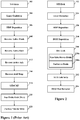
- a prior art front-end-of-line (FEOL) process fabrication to produce a silicon wafer with shallow trench isolation (STI) field oxide (FOX) wells and ready for active transistor element doping in the silicon substrate comprises the following steps.
- step 102 after a silicon wafer 320 has a thin layer of oxide 321 and a layer of silicon nitride 322 deposited thereon, the surface of the silicon wafer is patterned and etched to produce shallow trench isolation (STI) wells.
- STI shallow trench isolation
- step 104 the surface of a silicon wafer and the STI wells are oxidized to produce a liner thereon.
- step 106 a high density plasma (HDP) oxide is deposed on the oxidized liner.
- step 108 a reverse active mask is performed.
- step 110 a reverse active etch is performed.
- step 112 a reverse active ash (O 2 ) is performed.
- step 114 a reverse acid strip on the silicon wafer is performed.
- step 116 a shallow trench isolation (STI) chemical mechanical polish (CMP) is performed on the surface of the silicon wafer.
- step 118 a top oxide etch is performed.
- step 120 a nitride strip of the silicon wafer is preformed, leaving field oxides in the STI wells and exposed portions of the silicon wafer ready for the step of active transistor element doping in the silicon wafer substrate.
- STI shallow trench isolation
- CMP chemical mechanical polish
- a new, novel and non-obvious front-end-of-line (FEOL) process fabrication to produce a silicon wafer with shallow trench isolation (STI) field oxide (FOX) wells and ready for active transistor element doping in the silicon substrate comprises the following steps. Steps 102, 104 and 106 are substantially the same as described in Figure 1 above. Also refer to Figures 3-8 showing element numbers referenced hereinafter.
- STI shallow trench isolation
- step 208 is performed, by coating a partially planarizing organosilicate (DUO) 426 that is deposited onto the high density plasma (HDP) oxide 324.
- the DUO 426 is etched with, for example, but not limited to, a multiple step dry-plasma etch using common process gases, e.g., CF 4 , C 4 F 6 , C 5 F 8 , C 4 F 8 , O 2 , N 2 , Ar, etc.
- the first sub-step 210a is non-selective-to-oxide (CF 4 , O 2 , Ar) and the second sub-step 210b is partial-to-oxide (CsFs, O 2 , N 2 , Ar).
- the DUO 426 is striped off of all remaining areas silicon nitride using, for example but is not limited to, an oxidizing ash (O 2 ) and an HF strip, respectively.
- the profile of the remaining HDP 324 after etch and DUO removal is similar to the conventional reverse-mask process.
- the wafer then goes through CMP, TOP OXIDE ETCH, and NITRIDE STRIP just like what is done in other present technology semiconductor integrated circuit fabrication processes.
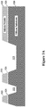
- FIG. 3 depicted is a schematic elevational cross-section of a silicon wafer 320 having a thin layer of oxide 321 and a layer of silicon nitride 322 deposited thereon, according to the teachings of this disclosure.
- FIG 3A depicted is a schematic elevational cross-section of the silicon wafer 320 after the step of shallow trench isolation (STI) etch 323.
- STI shallow trench isolation
- FIG. 3B depicted is a schematic elevational cross-section of a silicon wafer after performing the process steps of shallow trench isolation (STI) etch, liner oxidation and high-density plasma (HDP) deposition of the silicon wafer shown in Figures 3 and 3A .
- STI shallow trench isolation
- HDP high-density plasma
- HDP oxides may be used and are contemplated herein so long as those oxides have good fill characteristics. Even Spin-On-Glass may be used, for example.
- the STI etch profile and the HDP oxide 324 deposition leave the top of the silicon wafer with an irregular topography.
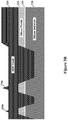
- FIG 4 depicted is a schematic elevational cross-section of the silicon wafer after performing the process step of spin-coating a layer of partially planarized organosilicate (DUO) onto the silicon wafer shown in Figure 3 , according to the invention.
- a layer of DUO 426 may be spin-coated onto the HDP oxide 324 which provides a somewhat planarizing effect thereto.
- the layer of DUO 426 may be selective or non-selective to the silicon oxide based upon etch process gases mix.
- a preferable characteristic is that the DUO etch rate may be tuned to be selective or non-selective to the oxide that is being etched. That allows the ability to planarise the oxide stack using only etching (no mask).
- FIG. 5 depicted is a schematic elevational cross-section of the silicon wafer after performing the process step of etching the DUO on the silicon wafer shown in Figure 4 , according to a specific example embodiment of this disclosure.
- the silicon wafer is etched in an oxide etcher, first with a plasma etch that non-selectively etches the DUO 426, using a mixture of CF 4 , O 2 and Ar.
- a second step then selectively etches the HDP Oxide 324 over the DUO 426 using gases such as C 4 F 6 , C 5 F 8 , C 4 F 8 , O 2 , N 2 , and/or Ar.
- the etching process stops when a certain depth is reached before coming into contact with the silicon nitride 322. This first etch helps to clear the DUO 426 from active areas (above silicon nitride) and level the stack more. The second etch then attempts to etch the HDP over active areas to an approximate thickness, optimum for CMP.
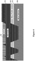
- Figure 6 illustrates a schematic elevational cross-section of the silicon wafer after performing the process step of removing the DUO on the silicon wafer shown in Figure 5 , according to a specific example embodiment of this disclosure.
- the DUO 426 may be removed by a dry O 2 ash and an HF clean.
- FIG. 7 depicted is a schematic elevational cross-section of the silicon wafer after performing the process step of shallow trench isolation (STI) chemical mechanical polishing (CMP), according to this disclosure.
- the STI CMP is a standard semiconductor integrated circuit process well known to one having ordinary skill in semiconductor integrated circuit manufacturing.
- the HDP oxide 324 is substantially planarized and removed from the layer of silicon nitride 322.
- FIG. 8 depicted is a schematic elevational cross-section of the silicon wafer after performing the process step of removing the silicon nitride to expose portions of the silicon substrate, according to the invention.
- the silicon nitride 322 may be removed by using a hot phosphoric acid bath, leaving the silicon substrate 320 exposed between field oxides (FOX) 624, ready for the step of active transistor element doping in the silicon substrate.
- FOX field oxides
- the aforementioned integrated circuit fabrication process could be used in other fabrication steps such as oxide CMP. It may not be economical as this process would add cost at the other steps.
- the liner oxidation is not silicon nitride; it is made of thermally-grown silicon dioxide. Any oxide deposition or fill may be used provided it meets the filling requirement for the given STI process.
- DUO is fairly unique because it was designed for fill and with the ability to change selectivity with different plasma etch processes.
- Bottom anti-reflective-coating BARC has been used in place of DUO for some processing, but is an organosilicate in the present invention.
Landscapes
- Engineering & Computer Science (AREA)
- Physics & Mathematics (AREA)
- Microelectronics & Electronic Packaging (AREA)
- General Physics & Mathematics (AREA)
- Manufacturing & Machinery (AREA)
- Computer Hardware Design (AREA)
- Condensed Matter Physics & Semiconductors (AREA)
- Power Engineering (AREA)
- Chemical & Material Sciences (AREA)
- Chemical Kinetics & Catalysis (AREA)
- General Chemical & Material Sciences (AREA)
- Inorganic Chemistry (AREA)
- Plasma & Fusion (AREA)
- Element Separation (AREA)
- Drying Of Semiconductors (AREA)
Applications Claiming Priority (2)
| Application Number | Priority Date | Filing Date | Title |
|---|---|---|---|
| US14/525,543 US9589828B2 (en) | 2014-10-28 | 2014-10-28 | Method for photolithography-free self-aligned reverse active etch |
| PCT/US2015/057469 WO2016069531A1 (en) | 2014-10-28 | 2015-10-27 | A method for photolithography-free self-aligned reverse active etch |
Publications (2)
| Publication Number | Publication Date |
|---|---|
| EP3213343A1 EP3213343A1 (en) | 2017-09-06 |
| EP3213343B1 true EP3213343B1 (en) | 2021-03-03 |
Family
ID=54477334
Family Applications (1)
| Application Number | Title | Priority Date | Filing Date |
|---|---|---|---|
| EP15791164.5A Active EP3213343B1 (en) | 2014-10-28 | 2015-10-27 | A method for photolithography-free self-aligned reverse active etch |
Country Status (8)
| Country | Link |
|---|---|
| US (1) | US9589828B2 (enExample) |
| EP (1) | EP3213343B1 (enExample) |
| JP (1) | JP2017535075A (enExample) |
| KR (1) | KR20170075716A (enExample) |
| CN (1) | CN107078022B (enExample) |
| SG (1) | SG11201702042YA (enExample) |
| TW (1) | TW201631650A (enExample) |
| WO (1) | WO2016069531A1 (enExample) |
Families Citing this family (1)
| Publication number | Priority date | Publication date | Assignee | Title |
|---|---|---|---|---|
| JP2019169581A (ja) * | 2018-03-23 | 2019-10-03 | 株式会社東芝 | 半導体装置の製造方法 |
Family Cites Families (13)
| Publication number | Priority date | Publication date | Assignee | Title |
|---|---|---|---|---|
| US6395620B1 (en) | 1996-10-08 | 2002-05-28 | Micron Technology, Inc. | Method for forming a planar surface over low density field areas on a semiconductor wafer |
| US5874345A (en) | 1996-11-18 | 1999-02-23 | International Business Machines Corporation | Method for planarizing TEOS SiO2 filled shallow isolation trenches |
| US5728621A (en) | 1997-04-28 | 1998-03-17 | Chartered Semiconductor Manufacturing Pte Ltd | Method for shallow trench isolation |
| US5976982A (en) * | 1997-06-27 | 1999-11-02 | Siemens Aktiengesellschaft | Methods for protecting device components from chemical mechanical polish induced defects |
| US6146975A (en) * | 1998-07-10 | 2000-11-14 | Lucent Technologies Inc. | Shallow trench isolation |
| TW413883B (en) * | 1999-02-26 | 2000-12-01 | Vanguard Int Semiconduct Corp | Method for using nitride hard mask for local reversed back-etching and CMP to solve the dishing effect encountered during CMP plantarization process |
| US6444581B1 (en) | 1999-07-15 | 2002-09-03 | International Business Machines Corporation | AB etch endpoint by ABFILL compensation |
| US6391781B1 (en) | 2000-01-06 | 2002-05-21 | Oki Electric Industry Co., Ltd. | Method of making a semiconductor device |
| TW436975B (en) * | 2000-03-23 | 2001-05-28 | United Microelectronics Corp | Shallow trench isolation process |
| US6593208B1 (en) * | 2001-02-14 | 2003-07-15 | Cypress Semiconductor Corp. | Method of uniform polish in shallow trench isolation process |
| US6617251B1 (en) * | 2001-06-19 | 2003-09-09 | Lsi Logic Corporation | Method of shallow trench isolation formation and planarization |
| US6638866B1 (en) * | 2001-10-18 | 2003-10-28 | Taiwan Semiconductor Manufacturing Company | Chemical-mechanical polishing (CMP) process for shallow trench isolation |
| US8426300B2 (en) * | 2010-12-02 | 2013-04-23 | International Business Machines Corporation | Self-aligned contact for replacement gate devices |
-
2014
- 2014-10-28 US US14/525,543 patent/US9589828B2/en active Active
-
2015
- 2015-10-27 KR KR1020177008459A patent/KR20170075716A/ko not_active Withdrawn
- 2015-10-27 CN CN201580057738.4A patent/CN107078022B/zh active Active
- 2015-10-27 SG SG11201702042YA patent/SG11201702042YA/en unknown
- 2015-10-27 WO PCT/US2015/057469 patent/WO2016069531A1/en not_active Ceased
- 2015-10-27 EP EP15791164.5A patent/EP3213343B1/en active Active
- 2015-10-27 JP JP2017520461A patent/JP2017535075A/ja active Pending
- 2015-10-28 TW TW104135483A patent/TW201631650A/zh unknown
Non-Patent Citations (1)
| Title |
|---|
| None * |
Also Published As
| Publication number | Publication date |
|---|---|
| TW201631650A (zh) | 2016-09-01 |
| CN107078022A (zh) | 2017-08-18 |
| WO2016069531A1 (en) | 2016-05-06 |
| KR20170075716A (ko) | 2017-07-03 |
| SG11201702042YA (en) | 2017-04-27 |
| JP2017535075A (ja) | 2017-11-24 |
| CN107078022B (zh) | 2021-01-15 |
| US20160118293A1 (en) | 2016-04-28 |
| US9589828B2 (en) | 2017-03-07 |
| EP3213343A1 (en) | 2017-09-06 |
Similar Documents
| Publication | Publication Date | Title |
|---|---|---|
| US10192956B2 (en) | Method for producing fin structures of a semiconductor device in a substrate | |
| EP3308394B1 (en) | Method of forming shallow trench isolation (sti) structures | |
| US20140349464A1 (en) | Method for forming dual sti structure | |
| US7786017B1 (en) | Utilizing inverse reactive ion etching lag in double patterning contact formation | |
| US6413828B1 (en) | Process using poly-buffered STI | |
| CN102280367B (zh) | 保护对准标记的方法及以此方法形成的半导体元件 | |
| EP3213343B1 (en) | A method for photolithography-free self-aligned reverse active etch | |
| US6667221B2 (en) | Method of manufacturing semiconductor device | |
| US6653202B1 (en) | Method of shallow trench isolation (STI) formation using amorphous carbon | |
| US6238997B1 (en) | Method of fabricating shallow trench isolation | |
| JP2009094379A (ja) | 半導体装置の製造方法 | |
| JP2003158179A (ja) | 半導体装置およびその製造方法 | |
| US20050148191A1 (en) | Method of manufacturing semiconductor device | |
| US20090170276A1 (en) | Method of Forming Trench of Semiconductor Device | |
| US7682928B2 (en) | Method of forming isolation layer of semiconductor device | |
| JP2017535075A5 (enExample) | ||
| KR100920000B1 (ko) | 반도체 소자의 컨택 형성 방법 | |
| KR100586072B1 (ko) | 얕은 트렌치 아이솔레이션 코너의 모우트 개선방법 | |
| KR100557035B1 (ko) | 반도체소자의 소자분리막 형성방법 | |
| KR100451519B1 (ko) | 반도체소자의 소자분리막 형성방법 | |
| KR20020088718A (ko) | 트렌치를 이용한 소자 분리 방법 | |
| JP2004103691A (ja) | 半導体装置の製造方法及び半導体装置 | |
| JP2007129037A (ja) | 半導体装置の製造方法 | |
| KR20020043807A (ko) | 반도체 소자의 격리 영역 형성 방법 | |
| KR20040087458A (ko) | 반도체소자의 소자분리막 형성방법 |
Legal Events
| Date | Code | Title | Description |
|---|---|---|---|
| STAA | Information on the status of an ep patent application or granted ep patent |
Free format text: STATUS: THE INTERNATIONAL PUBLICATION HAS BEEN MADE |
|
| PUAI | Public reference made under article 153(3) epc to a published international application that has entered the european phase |
Free format text: ORIGINAL CODE: 0009012 |
|
| STAA | Information on the status of an ep patent application or granted ep patent |
Free format text: STATUS: REQUEST FOR EXAMINATION WAS MADE |
|
| 17P | Request for examination filed |
Effective date: 20170524 |
|
| AK | Designated contracting states |
Kind code of ref document: A1 Designated state(s): AL AT BE BG CH CY CZ DE DK EE ES FI FR GB GR HR HU IE IS IT LI LT LU LV MC MK MT NL NO PL PT RO RS SE SI SK SM TR |
|
| AX | Request for extension of the european patent |
Extension state: BA ME |
|
| DAV | Request for validation of the european patent (deleted) | ||
| DAX | Request for extension of the european patent (deleted) | ||
| STAA | Information on the status of an ep patent application or granted ep patent |
Free format text: STATUS: EXAMINATION IS IN PROGRESS |
|
| 17Q | First examination report despatched |
Effective date: 20190221 |
|
| GRAP | Despatch of communication of intention to grant a patent |
Free format text: ORIGINAL CODE: EPIDOSNIGR1 |
|
| STAA | Information on the status of an ep patent application or granted ep patent |
Free format text: STATUS: GRANT OF PATENT IS INTENDED |
|
| INTG | Intention to grant announced |
Effective date: 20200925 |
|
| GRAS | Grant fee paid |
Free format text: ORIGINAL CODE: EPIDOSNIGR3 |
|
| GRAA | (expected) grant |
Free format text: ORIGINAL CODE: 0009210 |
|
| STAA | Information on the status of an ep patent application or granted ep patent |
Free format text: STATUS: THE PATENT HAS BEEN GRANTED |
|
| AK | Designated contracting states |
Kind code of ref document: B1 Designated state(s): AL AT BE BG CH CY CZ DE DK EE ES FI FR GB GR HR HU IE IS IT LI LT LU LV MC MK MT NL NO PL PT RO RS SE SI SK SM TR |
|
| REG | Reference to a national code |
Ref country code: GB Ref legal event code: FG4D |
|
| REG | Reference to a national code |
Ref country code: AT Ref legal event code: REF Ref document number: 1368136 Country of ref document: AT Kind code of ref document: T Effective date: 20210315 Ref country code: CH Ref legal event code: EP |
|
| REG | Reference to a national code |
Ref country code: DE Ref legal event code: R096 Ref document number: 602015066371 Country of ref document: DE |
|
| REG | Reference to a national code |
Ref country code: IE Ref legal event code: FG4D |
|
| REG | Reference to a national code |
Ref country code: LT Ref legal event code: MG9D |
|
| PG25 | Lapsed in a contracting state [announced via postgrant information from national office to epo] |
Ref country code: LT Free format text: LAPSE BECAUSE OF FAILURE TO SUBMIT A TRANSLATION OF THE DESCRIPTION OR TO PAY THE FEE WITHIN THE PRESCRIBED TIME-LIMIT Effective date: 20210303 Ref country code: HR Free format text: LAPSE BECAUSE OF FAILURE TO SUBMIT A TRANSLATION OF THE DESCRIPTION OR TO PAY THE FEE WITHIN THE PRESCRIBED TIME-LIMIT Effective date: 20210303 Ref country code: GR Free format text: LAPSE BECAUSE OF FAILURE TO SUBMIT A TRANSLATION OF THE DESCRIPTION OR TO PAY THE FEE WITHIN THE PRESCRIBED TIME-LIMIT Effective date: 20210604 Ref country code: FI Free format text: LAPSE BECAUSE OF FAILURE TO SUBMIT A TRANSLATION OF THE DESCRIPTION OR TO PAY THE FEE WITHIN THE PRESCRIBED TIME-LIMIT Effective date: 20210303 Ref country code: BG Free format text: LAPSE BECAUSE OF FAILURE TO SUBMIT A TRANSLATION OF THE DESCRIPTION OR TO PAY THE FEE WITHIN THE PRESCRIBED TIME-LIMIT Effective date: 20210603 Ref country code: NO Free format text: LAPSE BECAUSE OF FAILURE TO SUBMIT A TRANSLATION OF THE DESCRIPTION OR TO PAY THE FEE WITHIN THE PRESCRIBED TIME-LIMIT Effective date: 20210603 |
|
| REG | Reference to a national code |
Ref country code: NL Ref legal event code: MP Effective date: 20210303 |
|
| REG | Reference to a national code |
Ref country code: AT Ref legal event code: MK05 Ref document number: 1368136 Country of ref document: AT Kind code of ref document: T Effective date: 20210303 |
|
| PG25 | Lapsed in a contracting state [announced via postgrant information from national office to epo] |
Ref country code: PL Free format text: LAPSE BECAUSE OF FAILURE TO SUBMIT A TRANSLATION OF THE DESCRIPTION OR TO PAY THE FEE WITHIN THE PRESCRIBED TIME-LIMIT Effective date: 20210303 Ref country code: LV Free format text: LAPSE BECAUSE OF FAILURE TO SUBMIT A TRANSLATION OF THE DESCRIPTION OR TO PAY THE FEE WITHIN THE PRESCRIBED TIME-LIMIT Effective date: 20210303 Ref country code: RS Free format text: LAPSE BECAUSE OF FAILURE TO SUBMIT A TRANSLATION OF THE DESCRIPTION OR TO PAY THE FEE WITHIN THE PRESCRIBED TIME-LIMIT Effective date: 20210303 Ref country code: SE Free format text: LAPSE BECAUSE OF FAILURE TO SUBMIT A TRANSLATION OF THE DESCRIPTION OR TO PAY THE FEE WITHIN THE PRESCRIBED TIME-LIMIT Effective date: 20210303 |
|
| PG25 | Lapsed in a contracting state [announced via postgrant information from national office to epo] |
Ref country code: NL Free format text: LAPSE BECAUSE OF FAILURE TO SUBMIT A TRANSLATION OF THE DESCRIPTION OR TO PAY THE FEE WITHIN THE PRESCRIBED TIME-LIMIT Effective date: 20210303 |
|
| PG25 | Lapsed in a contracting state [announced via postgrant information from national office to epo] |
Ref country code: CZ Free format text: LAPSE BECAUSE OF FAILURE TO SUBMIT A TRANSLATION OF THE DESCRIPTION OR TO PAY THE FEE WITHIN THE PRESCRIBED TIME-LIMIT Effective date: 20210303 Ref country code: EE Free format text: LAPSE BECAUSE OF FAILURE TO SUBMIT A TRANSLATION OF THE DESCRIPTION OR TO PAY THE FEE WITHIN THE PRESCRIBED TIME-LIMIT Effective date: 20210303 Ref country code: SM Free format text: LAPSE BECAUSE OF FAILURE TO SUBMIT A TRANSLATION OF THE DESCRIPTION OR TO PAY THE FEE WITHIN THE PRESCRIBED TIME-LIMIT Effective date: 20210303 Ref country code: AT Free format text: LAPSE BECAUSE OF FAILURE TO SUBMIT A TRANSLATION OF THE DESCRIPTION OR TO PAY THE FEE WITHIN THE PRESCRIBED TIME-LIMIT Effective date: 20210303 |
|
| PG25 | Lapsed in a contracting state [announced via postgrant information from national office to epo] |
Ref country code: IS Free format text: LAPSE BECAUSE OF FAILURE TO SUBMIT A TRANSLATION OF THE DESCRIPTION OR TO PAY THE FEE WITHIN THE PRESCRIBED TIME-LIMIT Effective date: 20210703 Ref country code: PT Free format text: LAPSE BECAUSE OF FAILURE TO SUBMIT A TRANSLATION OF THE DESCRIPTION OR TO PAY THE FEE WITHIN THE PRESCRIBED TIME-LIMIT Effective date: 20210705 Ref country code: SK Free format text: LAPSE BECAUSE OF FAILURE TO SUBMIT A TRANSLATION OF THE DESCRIPTION OR TO PAY THE FEE WITHIN THE PRESCRIBED TIME-LIMIT Effective date: 20210303 Ref country code: RO Free format text: LAPSE BECAUSE OF FAILURE TO SUBMIT A TRANSLATION OF THE DESCRIPTION OR TO PAY THE FEE WITHIN THE PRESCRIBED TIME-LIMIT Effective date: 20210303 |
|
| REG | Reference to a national code |
Ref country code: DE Ref legal event code: R097 Ref document number: 602015066371 Country of ref document: DE |
|
| PLBE | No opposition filed within time limit |
Free format text: ORIGINAL CODE: 0009261 |
|
| STAA | Information on the status of an ep patent application or granted ep patent |
Free format text: STATUS: NO OPPOSITION FILED WITHIN TIME LIMIT |
|
| PG25 | Lapsed in a contracting state [announced via postgrant information from national office to epo] |
Ref country code: AL Free format text: LAPSE BECAUSE OF FAILURE TO SUBMIT A TRANSLATION OF THE DESCRIPTION OR TO PAY THE FEE WITHIN THE PRESCRIBED TIME-LIMIT Effective date: 20210303 Ref country code: ES Free format text: LAPSE BECAUSE OF FAILURE TO SUBMIT A TRANSLATION OF THE DESCRIPTION OR TO PAY THE FEE WITHIN THE PRESCRIBED TIME-LIMIT Effective date: 20210303 Ref country code: DK Free format text: LAPSE BECAUSE OF FAILURE TO SUBMIT A TRANSLATION OF THE DESCRIPTION OR TO PAY THE FEE WITHIN THE PRESCRIBED TIME-LIMIT Effective date: 20210303 |
|
| 26N | No opposition filed |
Effective date: 20211206 |
|
| PG25 | Lapsed in a contracting state [announced via postgrant information from national office to epo] |
Ref country code: SI Free format text: LAPSE BECAUSE OF FAILURE TO SUBMIT A TRANSLATION OF THE DESCRIPTION OR TO PAY THE FEE WITHIN THE PRESCRIBED TIME-LIMIT Effective date: 20210303 |
|
| PG25 | Lapsed in a contracting state [announced via postgrant information from national office to epo] |
Ref country code: IT Free format text: LAPSE BECAUSE OF FAILURE TO SUBMIT A TRANSLATION OF THE DESCRIPTION OR TO PAY THE FEE WITHIN THE PRESCRIBED TIME-LIMIT Effective date: 20210303 |
|
| REG | Reference to a national code |
Ref country code: CH Ref legal event code: PL |
|
| PG25 | Lapsed in a contracting state [announced via postgrant information from national office to epo] |
Ref country code: IS Free format text: LAPSE BECAUSE OF FAILURE TO SUBMIT A TRANSLATION OF THE DESCRIPTION OR TO PAY THE FEE WITHIN THE PRESCRIBED TIME-LIMIT Effective date: 20210703 |
|
| REG | Reference to a national code |
Ref country code: BE Ref legal event code: MM Effective date: 20211031 |
|
| GBPC | Gb: european patent ceased through non-payment of renewal fee |
Effective date: 20211027 |
|
| PG25 | Lapsed in a contracting state [announced via postgrant information from national office to epo] |
Ref country code: MC Free format text: LAPSE BECAUSE OF FAILURE TO SUBMIT A TRANSLATION OF THE DESCRIPTION OR TO PAY THE FEE WITHIN THE PRESCRIBED TIME-LIMIT Effective date: 20210303 |
|
| PG25 | Lapsed in a contracting state [announced via postgrant information from national office to epo] |
Ref country code: LU Free format text: LAPSE BECAUSE OF NON-PAYMENT OF DUE FEES Effective date: 20211027 Ref country code: GB Free format text: LAPSE BECAUSE OF NON-PAYMENT OF DUE FEES Effective date: 20211027 Ref country code: BE Free format text: LAPSE BECAUSE OF NON-PAYMENT OF DUE FEES Effective date: 20211031 |
|
| PG25 | Lapsed in a contracting state [announced via postgrant information from national office to epo] |
Ref country code: LI Free format text: LAPSE BECAUSE OF NON-PAYMENT OF DUE FEES Effective date: 20211031 Ref country code: CH Free format text: LAPSE BECAUSE OF NON-PAYMENT OF DUE FEES Effective date: 20211031 |
|
| PG25 | Lapsed in a contracting state [announced via postgrant information from national office to epo] |
Ref country code: FR Free format text: LAPSE BECAUSE OF NON-PAYMENT OF DUE FEES Effective date: 20211031 |
|
| PG25 | Lapsed in a contracting state [announced via postgrant information from national office to epo] |
Ref country code: IE Free format text: LAPSE BECAUSE OF NON-PAYMENT OF DUE FEES Effective date: 20211027 |
|
| PG25 | Lapsed in a contracting state [announced via postgrant information from national office to epo] |
Ref country code: HU Free format text: LAPSE BECAUSE OF FAILURE TO SUBMIT A TRANSLATION OF THE DESCRIPTION OR TO PAY THE FEE WITHIN THE PRESCRIBED TIME-LIMIT; INVALID AB INITIO Effective date: 20151027 |
|
| PG25 | Lapsed in a contracting state [announced via postgrant information from national office to epo] |
Ref country code: CY Free format text: LAPSE BECAUSE OF FAILURE TO SUBMIT A TRANSLATION OF THE DESCRIPTION OR TO PAY THE FEE WITHIN THE PRESCRIBED TIME-LIMIT Effective date: 20210303 |
|
| P01 | Opt-out of the competence of the unified patent court (upc) registered |
Effective date: 20230528 |
|
| PG25 | Lapsed in a contracting state [announced via postgrant information from national office to epo] |
Ref country code: MK Free format text: LAPSE BECAUSE OF FAILURE TO SUBMIT A TRANSLATION OF THE DESCRIPTION OR TO PAY THE FEE WITHIN THE PRESCRIBED TIME-LIMIT Effective date: 20210303 |
|
| PG25 | Lapsed in a contracting state [announced via postgrant information from national office to epo] |
Ref country code: MT Free format text: LAPSE BECAUSE OF FAILURE TO SUBMIT A TRANSLATION OF THE DESCRIPTION OR TO PAY THE FEE WITHIN THE PRESCRIBED TIME-LIMIT Effective date: 20210303 |
|
| PGFP | Annual fee paid to national office [announced via postgrant information from national office to epo] |
Ref country code: DE Payment date: 20240919 Year of fee payment: 10 |
|
| PG25 | Lapsed in a contracting state [announced via postgrant information from national office to epo] |
Ref country code: TR Free format text: LAPSE BECAUSE OF FAILURE TO SUBMIT A TRANSLATION OF THE DESCRIPTION OR TO PAY THE FEE WITHIN THE PRESCRIBED TIME-LIMIT Effective date: 20210303 |