EP3211056A1 - Compounds for use in opto-electrical devices - Google Patents
Compounds for use in opto-electrical devices Download PDFInfo
- Publication number
- EP3211056A1 EP3211056A1 EP17163676.4A EP17163676A EP3211056A1 EP 3211056 A1 EP3211056 A1 EP 3211056A1 EP 17163676 A EP17163676 A EP 17163676A EP 3211056 A1 EP3211056 A1 EP 3211056A1
- Authority
- EP
- European Patent Office
- Prior art keywords
- triazine
- composition according
- host material
- aryl
- opto
- Prior art date
- Legal status (The legal status is an assumption and is not a legal conclusion. Google has not performed a legal analysis and makes no representation as to the accuracy of the status listed.)
- Granted
Links
Classifications
-
- C—CHEMISTRY; METALLURGY
- C07—ORGANIC CHEMISTRY
- C07F—ACYCLIC, CARBOCYCLIC OR HETEROCYCLIC COMPOUNDS CONTAINING ELEMENTS OTHER THAN CARBON, HYDROGEN, HALOGEN, OXYGEN, NITROGEN, SULFUR, SELENIUM OR TELLURIUM
- C07F15/00—Compounds containing elements of Groups 8, 9, 10 or 18 of the Periodic Table
- C07F15/0006—Compounds containing elements of Groups 8, 9, 10 or 18 of the Periodic Table compounds of the platinum group
- C07F15/0033—Iridium compounds
-
- C—CHEMISTRY; METALLURGY
- C09—DYES; PAINTS; POLISHES; NATURAL RESINS; ADHESIVES; COMPOSITIONS NOT OTHERWISE PROVIDED FOR; APPLICATIONS OF MATERIALS NOT OTHERWISE PROVIDED FOR
- C09K—MATERIALS FOR MISCELLANEOUS APPLICATIONS, NOT PROVIDED FOR ELSEWHERE
- C09K11/00—Luminescent materials, e.g. electroluminescent or chemiluminescent
- C09K11/02—Use of particular materials as binders, particle coatings or suspension media therefor
- C09K11/025—Use of particular materials as binders, particle coatings or suspension media therefor non-luminescent particle coatings or suspension media
-
- C—CHEMISTRY; METALLURGY
- C09—DYES; PAINTS; POLISHES; NATURAL RESINS; ADHESIVES; COMPOSITIONS NOT OTHERWISE PROVIDED FOR; APPLICATIONS OF MATERIALS NOT OTHERWISE PROVIDED FOR
- C09K—MATERIALS FOR MISCELLANEOUS APPLICATIONS, NOT PROVIDED FOR ELSEWHERE
- C09K11/00—Luminescent materials, e.g. electroluminescent or chemiluminescent
- C09K11/06—Luminescent materials, e.g. electroluminescent or chemiluminescent containing organic luminescent materials
-
- H—ELECTRICITY
- H05—ELECTRIC TECHNIQUES NOT OTHERWISE PROVIDED FOR
- H05B—ELECTRIC HEATING; ELECTRIC LIGHT SOURCES NOT OTHERWISE PROVIDED FOR; CIRCUIT ARRANGEMENTS FOR ELECTRIC LIGHT SOURCES, IN GENERAL
- H05B33/00—Electroluminescent light sources
- H05B33/12—Light sources with substantially two-dimensional [2D] radiating surfaces
- H05B33/14—Light sources with substantially two-dimensional [2D] radiating surfaces characterised by the chemical or physical composition or the arrangement of the electroluminescent material, or by the simultaneous addition of the electroluminescent material in or onto the light source
-
- H—ELECTRICITY
- H10—SEMICONDUCTOR DEVICES; ELECTRIC SOLID-STATE DEVICES NOT OTHERWISE PROVIDED FOR
- H10K—ORGANIC ELECTRIC SOLID-STATE DEVICES
- H10K50/00—Organic light-emitting devices
- H10K50/10—OLEDs or polymer light-emitting diodes [PLED]
- H10K50/11—OLEDs or polymer light-emitting diodes [PLED] characterised by the electroluminescent [EL] layers
-
- H—ELECTRICITY
- H10—SEMICONDUCTOR DEVICES; ELECTRIC SOLID-STATE DEVICES NOT OTHERWISE PROVIDED FOR
- H10K—ORGANIC ELECTRIC SOLID-STATE DEVICES
- H10K50/00—Organic light-emitting devices
- H10K50/10—OLEDs or polymer light-emitting diodes [PLED]
- H10K50/11—OLEDs or polymer light-emitting diodes [PLED] characterised by the electroluminescent [EL] layers
- H10K50/12—OLEDs or polymer light-emitting diodes [PLED] characterised by the electroluminescent [EL] layers comprising dopants
-
- H—ELECTRICITY
- H10—SEMICONDUCTOR DEVICES; ELECTRIC SOLID-STATE DEVICES NOT OTHERWISE PROVIDED FOR
- H10K—ORGANIC ELECTRIC SOLID-STATE DEVICES
- H10K71/00—Manufacture or treatment specially adapted for the organic devices covered by this subclass
- H10K71/10—Deposition of organic active material
- H10K71/12—Deposition of organic active material using liquid deposition, e.g. spin coating
- H10K71/15—Deposition of organic active material using liquid deposition, e.g. spin coating characterised by the solvent used
-
- H—ELECTRICITY
- H10—SEMICONDUCTOR DEVICES; ELECTRIC SOLID-STATE DEVICES NOT OTHERWISE PROVIDED FOR
- H10K—ORGANIC ELECTRIC SOLID-STATE DEVICES
- H10K85/00—Organic materials used in the body or electrodes of devices covered by this subclass
- H10K85/10—Organic polymers or oligomers
- H10K85/111—Organic polymers or oligomers comprising aromatic, heteroaromatic, or aryl chains, e.g. polyaniline, polyphenylene or polyphenylene vinylene
-
- H—ELECTRICITY
- H10—SEMICONDUCTOR DEVICES; ELECTRIC SOLID-STATE DEVICES NOT OTHERWISE PROVIDED FOR
- H10K—ORGANIC ELECTRIC SOLID-STATE DEVICES
- H10K85/00—Organic materials used in the body or electrodes of devices covered by this subclass
- H10K85/10—Organic polymers or oligomers
- H10K85/151—Copolymers
-
- H—ELECTRICITY
- H10—SEMICONDUCTOR DEVICES; ELECTRIC SOLID-STATE DEVICES NOT OTHERWISE PROVIDED FOR
- H10K—ORGANIC ELECTRIC SOLID-STATE DEVICES
- H10K85/00—Organic materials used in the body or electrodes of devices covered by this subclass
- H10K85/20—Carbon compounds, e.g. carbon nanotubes or fullerenes
- H10K85/221—Carbon nanotubes
- H10K85/225—Carbon nanotubes comprising substituents
-
- H—ELECTRICITY
- H10—SEMICONDUCTOR DEVICES; ELECTRIC SOLID-STATE DEVICES NOT OTHERWISE PROVIDED FOR
- H10K—ORGANIC ELECTRIC SOLID-STATE DEVICES
- H10K85/00—Organic materials used in the body or electrodes of devices covered by this subclass
- H10K85/30—Coordination compounds
- H10K85/341—Transition metal complexes, e.g. Ru(II)polypyridine complexes
- H10K85/342—Transition metal complexes, e.g. Ru(II)polypyridine complexes comprising iridium
-
- H—ELECTRICITY
- H10—SEMICONDUCTOR DEVICES; ELECTRIC SOLID-STATE DEVICES NOT OTHERWISE PROVIDED FOR
- H10K—ORGANIC ELECTRIC SOLID-STATE DEVICES
- H10K85/00—Organic materials used in the body or electrodes of devices covered by this subclass
- H10K85/60—Organic compounds having low molecular weight
- H10K85/649—Aromatic compounds comprising a hetero atom
- H10K85/654—Aromatic compounds comprising a hetero atom comprising only nitrogen as heteroatom
-
- C—CHEMISTRY; METALLURGY
- C09—DYES; PAINTS; POLISHES; NATURAL RESINS; ADHESIVES; COMPOSITIONS NOT OTHERWISE PROVIDED FOR; APPLICATIONS OF MATERIALS NOT OTHERWISE PROVIDED FOR
- C09K—MATERIALS FOR MISCELLANEOUS APPLICATIONS, NOT PROVIDED FOR ELSEWHERE
- C09K2211/00—Chemical nature of organic luminescent or tenebrescent compounds
- C09K2211/10—Non-macromolecular compounds
- C09K2211/1018—Heterocyclic compounds
- C09K2211/1025—Heterocyclic compounds characterised by ligands
- C09K2211/1059—Heterocyclic compounds characterised by ligands containing three nitrogen atoms as heteroatoms
-
- C—CHEMISTRY; METALLURGY
- C09—DYES; PAINTS; POLISHES; NATURAL RESINS; ADHESIVES; COMPOSITIONS NOT OTHERWISE PROVIDED FOR; APPLICATIONS OF MATERIALS NOT OTHERWISE PROVIDED FOR
- C09K—MATERIALS FOR MISCELLANEOUS APPLICATIONS, NOT PROVIDED FOR ELSEWHERE
- C09K2211/00—Chemical nature of organic luminescent or tenebrescent compounds
- C09K2211/18—Metal complexes
- C09K2211/185—Metal complexes of the platinum group, i.e. Os, Ir, Pt, Ru, Rh or Pd
-
- H—ELECTRICITY
- H10—SEMICONDUCTOR DEVICES; ELECTRIC SOLID-STATE DEVICES NOT OTHERWISE PROVIDED FOR
- H10K—ORGANIC ELECTRIC SOLID-STATE DEVICES
- H10K2101/00—Properties of the organic materials covered by group H10K85/00
- H10K2101/10—Triplet emission
-
- H—ELECTRICITY
- H10—SEMICONDUCTOR DEVICES; ELECTRIC SOLID-STATE DEVICES NOT OTHERWISE PROVIDED FOR
- H10K—ORGANIC ELECTRIC SOLID-STATE DEVICES
- H10K2101/00—Properties of the organic materials covered by group H10K85/00
- H10K2101/40—Interrelation of parameters between multiple constituent active layers or sublayers, e.g. HOMO values in adjacent layers
-
- H—ELECTRICITY
- H10—SEMICONDUCTOR DEVICES; ELECTRIC SOLID-STATE DEVICES NOT OTHERWISE PROVIDED FOR
- H10K—ORGANIC ELECTRIC SOLID-STATE DEVICES
- H10K71/00—Manufacture or treatment specially adapted for the organic devices covered by this subclass
- H10K71/10—Deposition of organic active material
- H10K71/12—Deposition of organic active material using liquid deposition, e.g. spin coating
Definitions
- This invention relates to compositions comprising triazine host compounds for use in fabricating phosphorescent opto-electrical devices, and methods of fabricating opto-electrical devices using these compositions.
- a typical organic light-emissive device is fabricated on a glass or plastic substrate coated with a transparent first electrode such as indium-tin-oxide("ITO").
- a transparent first electrode such as indium-tin-oxide("ITO").
- a layer of a thin film of at least one electroluminescent organic material covers the first electrode.
- a cathode covers the layer of electroluminescent organic material.
- the cathode is typically a metal or alloy and may comprise a single layer, such as aluminium, or a plurality of layers such as calcium and aluminium. Other layers can be added to the device, for example to improve charge injection from the electrodes to the electroluminescent material.
- WO 02/083760 discloses copolymers for use as charge transporting materials and fluorescent emissive materials in organic opto-electrical devices.
- the co-polymers comprise a first repeat unit which may be a triazine unit as shown in formula (a): wherein R" is selected from hydrogen, branched or linear C1-C20 alkyl or alkoxy.
- a problem with known host-fluorescent emitter systems is that the host may quench emission from the fluorescent emitter. It is advantageous to provide a host having a higher LUMO than that of the emitter to inject electrons into the emitter. It is advantageous to provide a host having a lower HOMO than that of the emitter to inject holes into the emitter. Accordingly, there is a need to produce materials with a large band gap between the HOMO and LUMO for use as hosts in fluorescent systems.
- the present invention provides triazine compounds which can be solution processed and which produce films having a good morphology and tunable physical properties for use in opto-electrical devices.
- the triazine compounds of the present invention have both a deep LUMO and a deep HOMO.
- the triazine compounds readily accept electrons but do not readily accept holes in an opto-electrical device.
- these compounds serve as electron transporting host materials for emissive materials without quenching emission from the emissive materials.
- the electrical characteristics of the triazine compounds of the present invention are such that in additional to acting as good host materials, they can also be used as blue emissive materials, electron transporting materials (either in a separate electron transporting layer located between the cathode and the emissive layer of a device or incorporated into the emissive layer of the device as a blend with an emissive material or bonded to the emissive material) and/or hole blocking materials (located in a layer between the emissive layer and the cathode in a device). Furthermore, the low LUMO of the triazine compounds also allows cathode materials with higher work-functions to be used.
- triphenyl triazine moiety that is common to the above structures is more chemically and electrochemically inert and is therefore more stable in the device when compared with standard hosts, for example CBP, optionally substituted with solubilising groups such as alkyl or alkoxy groups.
- the triazines are also advantageous as they have good electron transport properties, which make them much more suitable for use in common device structures, as they can be used in conjunction with an electron-blocking/hole transporting layer disposed between the light-emissive layer and a hole injecting layer. There is also no need for a hole-blocking/electron transporting layer disposed between the light-emissive layer and the cathode, which is commonly required in phosphorescent devices.
- the phosphorescent moiety is a green emitter.
- Known hosts for green emitters such as solution processable polyfluorene host materials generally have triplet levels that are too low to be efficient hosts for green phosphorescent moieties.
- embodiments of the present invention are efficient host materials for green phosphorescent moieties.
- the solution processable triazines may also be used as hosts for red phosphorescent moieties.
- these monomers can be used to prepare wide band-gap polymers with similarly good electron injection / transport, but that avoid the need for polyfluorenes that generally have triplet levels that are too low to use as a green phosphorescent host.
- This polymer has the processing properties of a conjugated polymer with the triplet band-gap and electron injection properties of the triazine.
- Other monomers could also be introduced to fine-tune the charge injection / conduction properties, or to add luminescent centres.
- the cathode preferably has a workfunction of less than 3.5 eV, more preferably less than 3.2 eV, yet more preferably less than 3 eV, most preferably less than 2.8 eV.
- Each of Ar 4 and Ar 5 may carry one or more substituents.
- Particularly preferred substituents include fluorine or trifluoromethyl which may be used to blue-shift the emission of the complex as disclosed in WO 02/45466 , WO 02/44189 , US 2002-117662 and US 2002-182441 ; alkyl or alkoxy groups as disclosed in JP 2002-324679 ; carbazole which may be used to assist hole transport to the complex when used as an emissive material as disclosed in WO 02/81448 ; bromine, chlorine or iodine which can serve to functionalise the ligand for attachment of further groups as disclosed in WO 02/68435 and EP 1245659 ; and dendrons which may be used to obtain or enhance solution processability of the metal complex as disclosed in WO 02/66552 .
- Main group metal complexes show ligand based, or charge transfer emission.
- the emission colour is determined by the choice of ligand as well as the metal.
- Embodiments of the present invention can also be used as hosts for fluorescent emitters.
- a wide range of fluorescent low molecular weight metal complexes may be used with the present invention.
- Suitable ligands for di or trivalent metals include: oxinoids, e. g.
Landscapes
- Chemical & Material Sciences (AREA)
- Engineering & Computer Science (AREA)
- Materials Engineering (AREA)
- Organic Chemistry (AREA)
- Physics & Mathematics (AREA)
- Optics & Photonics (AREA)
- Nanotechnology (AREA)
- Manufacturing & Machinery (AREA)
- Spectroscopy & Molecular Physics (AREA)
- Crystallography & Structural Chemistry (AREA)
- Inorganic Chemistry (AREA)
- Electroluminescent Light Sources (AREA)
Abstract
Description
- This invention relates to compositions comprising triazine host compounds for use in fabricating phosphorescent opto-electrical devices, and methods of fabricating opto-electrical devices using these compositions.
- One class of opto-electrical devices is that using an organic material for light emission or detection. The basic structure of these devices is a light emissive organic layer, for instance a film of a poly (p-phenylenevinylene) ("PPV") or polyfluorene, sandwiched between a cathode for injecting negative charge carriers (electrons) and an anode for injecting positive charge carriers (holes) into the organic layer. The electrons and holes combine in the organic layer generating photons. In
WO 90/13148 US 4,539,507 the organic light-emissive material is of the class known as small molecule materials, such as (8-hydroxyquinoline) aluminium ("Alq3"). In a practical device one of the electrodes is transparent, to allow the photons to escape the device. - A typical organic light-emissive device ("OLED") is fabricated on a glass or plastic substrate coated with a transparent first electrode such as indium-tin-oxide("ITO"). A layer of a thin film of at least one electroluminescent organic material covers the first electrode. Finally, a cathode covers the layer of electroluminescent organic material. The cathode is typically a metal or alloy and may comprise a single layer, such as aluminium, or a plurality of layers such as calcium and aluminium. Other layers can be added to the device, for example to improve charge injection from the electrodes to the electroluminescent material. For example, a hole injection layer such as poly (ethylene dioxythiophene) /polystyrene sulfonate (PEDOT-PSS) or polyaniline may be provided between the anode and the electroluminescent material. When a voltage is applied between the electrodes from a power supply one of the electrodes acts as a cathode and the other as an anode.
- In operation, holes are injected into the device through the anode and electrons are injected into the device through the cathode. The holes and electrons combine in the organic electroluminescent layer to form an exciton which then undergoes radiative decay to give light.
- For organic semiconductors, important characteristics are the binding energies, measured with respect to the vacuum level of the electronic energy levels, particularly the "highest occupied molecular orbital" (HOMO) and the "lowest unoccupied molecular orbital" (LUMO) level. These can be estimated from measurements of photoemission and particularly measurements of the electrochemical potentials for oxidation and reduction. It is well understood in this field that such energies are affected by a number of factors, such as the local environment near an interface, and the point on the curve (peak) from which the value is determined. Accordingly, the use of such values is indicative rather than quantitative.
- The optical and electronic properties of an organic semiconductor are highly dependent on the energy of the aforementioned HOMO and LUMO levels. Furthermore, these energy levels are highly dependent on the chemical structure of the organic semiconductor. By selecting suitable materials, or combinations of materials, device performance can be improved.
- For example, one way of improving efficiency of devices is to provide hole and electron transporting materials.
WO 99/48610 - Although there has been much improvement in the efficiency of devices using charge transporting materials, there is always a desire to develop new charge transporting materials to further improving efficiency when compared with existing devices.
-
WO 02/083760 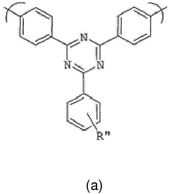
- The copolymers comprise a second repeat unit which may be selected from the group consisting of optionally substituted phenylenes, fluorenes, heteroaryls and triarylamines.
- Triazines as components of blue electroluminescent devices are disclosed in
WO 2004/077885 .
US 6821643 discloses arylated triazines that are deposited by evaporation to form a blue fluorescent light-emitting layer or an electron transport layer of an OLED.
US 6,352,791 discloses arylated triazines that are deposited by evaporation to form an electron transport layer of an OLED.
WO 2005/105950 discloses certain tri-substituted triazines used as a blue fluorescent light-emitting layer of an OLED.
EP 1385221 discloses a light-emitting device comprising a luminescent region comprising an anthracene derivative compound and a triazine derivative compound. - Phosphorescent materials are also useful and in some applications may be preferable to fluorescent materials. One type of phosphorescent material comprises a host and a phosphorescent emitter in the host. The emitter may be bonded to the host or provided as a separate component in a blend.
- Numerous hosts for phosphorescent emitters are described in the prior art including "small molecule" hosts such as 4,4'-bis(carbazol-9-yl)biphenyl), known as CBP, and (4,4',4"-tris(carbazol-9-yl)triphenylamine), known as TCTA, disclosed in Ikai et al. (Appl. Phys. Lett., 79 no. 2, 2001, 156); and triarylamines such as tris-4-(N-3-methylphenyl-N-phenyl)phenylamine, known as MTDATA. Homopolymers are also known as hosts, in particular poly(vinyl carbazole) disclosed in, for example, Appl. Phys. Lett. 2000, 77(15), 2280; polyfluorenes in Synth. Met. 2001, 116, 379, Phys. Rev. B 2001, 63, 235206 and Appl. Phys. Lett. 2003, 82(7), 1006; poly[4-(N-4-vinylbenzyloxyethyl, N-methylamino)-N-(2,5-di-tert-butylphenylnapthalimide] in Adv. Mater. 1999, 11(4), 285; and poly(para-phenylenes) in J. Mater. Chem. 2003, 13,50-55.
- A problem with known host-phosphor systems is that the host may quench emission from the phosphor. In general, the lower the triplet energy level of the host (relative to the phosphor) then the more likely quenching will occur. Polymerisation can exacerbate this problem by reducing the triplet energy level to below that of a monomer when forming a host polymer. Accordingly, there is a need to produce materials with a high triplet energy level for use as hosts in phosphorescent systems.
-
JP 2005071983 
- In Chemistry of Materials (2004), 16(7), 1285-1291 a tris-carbazolyl compound and other arylamino-substituted triazines are disclosed as hosts for Irppy in OLEDs, for example:

-
WO 2005029923 discloses tris-benzimidazolyl substituted triazine as a host for the red phosphor, Ir(piq):
-
US2005/0287393 discloses a light emissive composition comprising a phosphorescent dopant and a host including a carbazole compound and a small molecule triazine compound. Exemplary triazine compounds are given as 2,4,6-tris(diarylamino)-1,3,5-triazine, 2,4,6-tris(diphenylamino)-1,3,5-triazine, 2,4,6-tricarbazolo-1,3,5-triazine, 2,4,6-tris(N-phenyl-2-naphthylamino)-1,3,5-triazine, 2,4,6-tris(N-pheyl-1-naphthyl amino)-1,3,5-triazine, or 2,4,6-trisbiphenyl-1,3,5-triazine. - All of the above-identified small molecule triazines for use as hosts in phosphorescent compositions are amino derivative except for the last example, 2,4,6-trisbiphenyl-1,3,5-triazine, given in the list of examples in
US2005/0287393 . The amino derivatives all have a nitrogen atom directly bonding the aryl substituents to the central triazine ring. However, the present applicant proposes that this nitrogen linkage is not completely stable which can reduce the lifetime of these compositions. Furthermore, none of the above-identified small molecule compounds are soluble enough to be readily solution processed and instead these compounds are more suited to vacuum thermal deposition. - Host-emitter systems are not limited to phosphorescent devices. A wide range of fluorescent low molecular weight metal complexes are known and have been demonstrated in organic light emitting devices [see, e. g., Macromol. Sym. 125 (1997) 1-48,
US-A 5,150,006 ,US-A 6,083,634 andUS-A 5,432,014 ]. - As with phosphorescent systems, a problem with known host-fluorescent emitter systems is that the host may quench emission from the fluorescent emitter. It is advantageous to provide a host having a higher LUMO than that of the emitter to inject electrons into the emitter. It is advantageous to provide a host having a lower HOMO than that of the emitter to inject holes into the emitter. Accordingly, there is a need to produce materials with a large band gap between the HOMO and LUMO for use as hosts in fluorescent systems.
- Another factor affecting the performance of opto-electonic devices is morphology of the films which make up the device. For semiconductive organic materials it is advantageous to have an amorphous rather than a crystalline film. However, it is desirable not to have too much disorder in the film in order to achieve a device with better performance. Accordingly, there is a desire to produce materials with better film forming characteristics.
- It is an aim of the present invention to solve one or more of the problems outlined above.
- According to a first aspect of the present invention there is provided a composition for use in fabricating opto-electrical devices comprising a solution processable triazine host material and a phosphorescent moiety.
In one embodiment, the solution processable triazine host material is a small molecule triazine compound.
In another embodiment, the solution processable triazine host material is a polymer comprising a triazine repeat unit. - By "small molecule" we mean non-polymeric. The term "small molecule" is often used in this art to have this meaning as there are two main families of organic opto-electrical materials: polymers and small molecules. Oligomers consist of 1 to 10 repeat units, more preferably, 1 to 5 repeat units.
Preferably, the triazine host material comprises a solubilising substituent.
By "solubilizing substituent" we mean a substituent which renders the triazine sufficiently soluble in organic solvents that it can be solution processed to fabricate an opto-electrical device by, for example, ink-jet printing or spin-coating. Generally, compounds must be soluble to a concentration above 8 mg ml-1, preferably above 10mg ml-1, in order for them to be solution processed in a device manufacturing method. Organic solvents suitable for opto-electrical device fabrication include xylene, toluene, chlorobenzene, chloroform or tetrahydrofuran but preferably toluene or xylene. The prior art compound 2,4,6-tris(biphenyl)-1,3,5-triazine has a solubility <5 mg ml-1 in all of these solvents and thus is not a suitable material for fabricating an OLED device by solution processing. - It has been found that by providing a solubilising substituent on a small molecule triazine compound, the compound can be readily solution processed. As such, the compositions comprising small molecule triazine compounds of the present invention can be deposited to form a film by, for example, ink-jet printing or spin-coating rather than thermal vapour deposition.
- Furthermore, it has been found that solubilising substituents reduce the crystallinity of a film formed by depositing triazine compounds when compared with prior art small molecule triazine compounds resulting in a better film morphology. In addition, the solubilizing substituent can be used to tune the physical properties of a film.
- Thus, the present invention provides triazine compounds which can be solution processed and which produce films having a good morphology and tunable physical properties for use in opto-electrical devices. Furthermore, the triazine compounds of the present invention have both a deep LUMO and a deep HOMO. As such, the triazine compounds readily accept electrons but do not readily accept holes in an opto-electrical device. Moreover, these compounds serve as electron transporting host materials for emissive materials without quenching emission from the emissive materials. Preferably, the LUMO level is intermediate in energy between the fermi level of the electron injecting material in the cathode and the LUMO level (or triplet level in phosphorescent emissive materials) of the emissive material or at least not significantly higher than the fermi level of the electron injecting material or significantly lower than the LUMO (or triplet level) of the emissive material as to require a high drive voltage. Preferably, the HOMO level of the triazine compounds is lower than the HOMO level of the emissive material. Due to the poor hole accepting/hole transporting properties of the triazines, it is preferable to use them in conjunction with a hole transporting material or with an emissive material which is a good hole transporting material.
- The LUMO levels of the triazine compounds are preferably intermediate in energy between the injecting cathode and the emitter. If a barrier to electron injection is present it is preferably not more than 0.4 eV above the work function of the cathode. The HOMO level of the triazine should be such as to maintain an optical band-gap large enough to maintain a triplet level energy gap that will not quench the phosphorescence from the emitter species.
- The electrical characteristics of the triazine compounds of the present invention are such that in additional to acting as good host materials, they can also be used as blue emissive materials, electron transporting materials (either in a separate electron transporting layer located between the cathode and the emissive layer of a device or incorporated into the emissive layer of the device as a blend with an emissive material or bonded to the emissive material) and/or hole blocking materials (located in a layer between the emissive layer and the cathode in a device). Furthermore, the low LUMO of the triazine compounds also allows cathode materials with higher work-functions to be used. Triazine compounds with LUMO level of, for example, 2.8eV will allow the use of higher work function cathodes where the energy gap is not greater than 0.4 eV. Thus cathode materials with work functions in the range 2.6 to 3.2 eV are preferred.
- Preferably, the at least one solubilizing substituent comprises a C4 - C20 alkyl chain. It has been found that alkyl chains within this range render the triazine compound sufficiently soluble to be readily solution processed and form films having a good morphology. The length and composition of the alkyl chain can be tailored to tune the physical properties of the film according to its specific use.
- Preferably, the central triazine ring is substituted with at least one aryl group. Most preferably, the aryl group is directly bonded to the central triazine ring. The aryl group may be a phenyl ring. Most preferably, the triazine compound is a tris-aryl triazine with at least one of the aryl groups having a solubilizing substituent bonded thereto. More preferably, two or three of the aryl groups have solubilizing substituents bonded thereto. The solubilizing groups may be the same or different.
- It has been found that tris-aryl triazine compounds having solubilizing groups thereon form films with a good physical morphology and good physical properties. In particular, the aryl groups and the solubilising groups provide a film which is amorphous but does not have too much disorder. These films have better opto-electrical properties and produce a device with better performance.
- Preferably, the at least one solubilizing substituent is directly bonded to the central triazine ring via a carbon atom. As previously stated, the prior art triazine compounds which have substituents bonded to the central triazine ring via a nitrogen atom may be unstable in an opto-electrical device thus reducing the lifetime of the device. The nitrogen linking atom may act as a reactive site for substitution of the substituent during device operation. In contrast, carbon bonded substituents according to embodiments of the present invention are more stable in an opto-electrical device.
- According to embodiments of the present invention, the triazine structures are simple triaryl substituted compounds without heteroatom linkages but with alkyl substituents or preferably aryl substituents having alkyl groups thereon, selected to allow tuning of the physical properties of the films formed using these structures, e.g. Tg>150 °C, good film morphology, appropriate HOMO and LUMO levels etc. An example of such a structure is shown in the formula below:


- The specific compounds shown above have been device tested as host materials for green phosphorescent materials and exhibit superior lifetime performance to known solution processable green hosts. It is also envisaged that embodiments of the present invention may be utilized as hosts for red phosphorescent materials.
- It is believed that the triphenyl triazine moiety that is common to the above structures is more chemically and electrochemically inert and is therefore more stable in the device when compared with standard hosts, for example CBP, optionally substituted with solubilising groups such as alkyl or alkoxy groups. The triazines are also advantageous as they have good electron transport properties, which make them much more suitable for use in common device structures, as they can be used in conjunction with an electron-blocking/hole transporting layer disposed between the light-emissive layer and a hole injecting layer. There is also no need for a hole-blocking/electron transporting layer disposed between the light-emissive layer and the cathode, which is commonly required in phosphorescent devices.
- One potential problem with the compounds shown above is that their energy levels might be too deep for some applications. However, with appropriate substitution (with e.g. amines) optimum energy levels can be obtained for these applications. It should be noted that amine substituents should not be directly bonded to the central triazine ring via a nitrogen atom for the reasons discussed previously. Alternatively any other functional groups with suitable electron donating or electron withdrawing groups may be used as required including but not limited to for example Fluoro-aryl, perfluoroaryl, alkyl-aryl or alkoxy-aryl groups.
- It has been found that solution processable triazine materials are excellent hosts for phosphorescent emissive materials as their deep LUMO provide enhanced electron-injection/transport and their wide triplet band-gap reduces quenching. The advantageous features described in relation to the first aspect of the invention are also applicable to the second aspect of the invention.
- The triazine units may be provided in a copolymer with, for example, hole transporting units such as a triaryl amine or a twisted co-monomer which will maintain the triplet level of the polymer so as not to quench the emission from the phosphorescent emitter. For example,

- Alternatively, or additionally, the co-polymer may comprise the phosphorescent moiety. The phosphorescent moiety may be provided in the polymer backbone or in a pendent side chain.
- Preferably the phosphorescent moiety is a green emitter. Known hosts for green emitters such as solution processable polyfluorene host materials generally have triplet levels that are too low to be efficient hosts for green phosphorescent moieties. In contrast, embodiments of the present invention are efficient host materials for green phosphorescent moieties. However, it is envisaged that the solution processable triazines may also be used as hosts for red phosphorescent moieties.
- An example of a triazine monomer suitable for fabricating polymer hosts is shown below:

- As a host material for green phosphorescence, these monomers can be used to prepare wide band-gap polymers with similarly good electron injection / transport, but that avoid the need for polyfluorenes that generally have triplet levels that are too low to use as a green phosphorescent host. For example:

- According to a third aspect of the present invention there is provided a method of fabricating an opto-electrical device, the method comprising the steps: depositing from solution, on a substrate comprising a first electrode for injecting charge carriers of a first polarity, a composition according to the first aspect of the present invention; and depositing thereover a second electrode for injecting charge carriers of a second polarity opposite to the first polarity.
- According to a fourth aspect of the present invention there is provided an opto-electrical device comprising: a substrate; a first electrode disposed over the substrate for injecting charge carriers of a first polarity; a layer disposed over the first electrode comprising a composition according to the first aspect of the present invention; and a second electrode disposed thereover for injecting charge carriers of a second polarity opposite to the first polarity.
- Embodiments of the present invention will now be described by way of example only with reference to the accompanying drawing in which:
- Figure 1 shows an organic light emitting device according to an embodiment of the present invention.
- The device shown in Figure 1 comprises a transparent glass or plastic substrate 1, an anode 2 of indium tin oxide and a cathode 4. An electroluminescent layer 3 is provided between anode 2 and cathode 4.
- Further layers may be located between anode 2 and cathode 3, such as charge transporting, charge injecting or charge blocking layers.
- In particular, it is desirable to provide a conductive hole injection layer formed of a doped organic material located between the anode 2 and the electroluminescent layer 3 to assist hole injection from the anode into the layer or layers of semiconducting polymer. Examples of doped organic hole injection materials include: poly(ethylene dioxythiophene) (PEDT), in particular PEDT doped with a charge-balancing polyacid such as polystyrene sulfonate (PSS) as disclosed in
EP 0901176 andEP 0947123 , polyacrylic acid or a fluorinated sulfonic acid, for example Nafion ®; polyaniline as disclosed inUS 5723873 andUS 5798170 ; and poly(thienothiophene). Conductive inorganic materials may also be employed as hole injection layers. Suitable inorganic materials include transition metal oxides such as VOx MoOx and RuOx as disclosed in Journal of Physics D: Applied Physics (1996), 29(11), 2750-2753. - If present, a hole transporting layer located between anode 2 and electroluminescent layer 3 preferably has a HOMO level of less than or equal to 5.5 eV, more preferably around 4.8-5.5 eV.
- If present, an electron transporting layer located between electroluminescent layer 3 and cathode 4 preferably has a LUMO level of around 3-3.5 eV.
- Electroluminescent layer 3 may consist of the electroluminescent material alone or may comprise the electroluminescent material in combination with one or more further materials. In particular, the electroluminescent material may be blended with hole and / or electron transporting materials as disclosed in, for example,
WO 99/48160 - Cathode 4 is selected from materials that have a workfunction allowing injection of electrons into the electroluminescent layer. Other factors influence the selection of the cathode such as the possibility of adverse interactions between the cathode and the electroluminescent material. The cathode may consist of a single material such as a layer of aluminium. Alternatively, it may comprise a plurality of metals, for example a bilayer of a low workfunction material and a high workfunction material such as calcium and aluminium as disclosed in
WO 98/10621 WO 98/57381 WO 02/84759 WO 00/48258 - Optical devices tend to be sensitive to moisture and oxygen. Accordingly, the substrate preferably has good barrier properties for prevention of ingress of moisture and oxygen into the device. The substrate is commonly glass, however alternative substrates may be used, in particular where flexibility of the device is desirable. For example, the substrate may comprise a plastic as in
US 6268695 which discloses a substrate of alternating plastic and barrier layers or a laminate of thin glass and plastic as disclosed inEP 0949850 . - The device is preferably encapsulated with an encapsulant (not shown) to prevent ingress of moisture and oxygen. Suitable encapsulants include a sheet of glass, films having suitable barrier properties such as alternating stacks of polymer and dielectric as disclosed in, for example,
WO 01/81649 WO 01/19142 - In a practical device, at least one of the electrodes is semi-transparent in order that light may be absorbed (in the case of a photoresponsive device) or emitted (in the case of an OLED). Where the anode is transparent, it typically comprises indium tin oxide. Examples of transparent cathodes are disclosed in, for example,
GB 2348316 - The embodiment of Figure 1 illustrates a device wherein the device is formed by firstly forming an anode on a substrate followed by deposition of an electroluminescent layer and a cathode. However it will be appreciated that the device of the invention could also be formed by firstly forming a cathode on a substrate followed by deposition of an electroluminescent layer and an anode.
- Semiconductive polymers may be provided for the purpose of charge transport, emission or as host polymers. A range of repeat units for such polymers are described in more detail below. These polymers may be used separately from the triazines of the present invention (for example as a separate emissive centre in a multicolour device).
- Alternatively, these repeat units may be used in combination with the triazines. For example, the solution processable triazine host material according to the second aspect of the invention may comprise a triazine repeat unit and one or more further repeat units selected from those described below. In this case, it will be appreciated that the polymer formed from such repeat units used in combination with the triazine repeat units must have a triplet energy higher than that of the phosphorescent dopant.
- Polymers may comprise a first repeat unit selected from arylene repeat units, in particular: 1,4-phenylene repeat units as disclosed in J. Appl. Phys. 1996, 79, 934; fluorene repeat units as disclosed in
EP 0842208 ; indenofluorene repeat units as disclosed in, for example, Macromolecules 2000, 33(6), 2016-2020; and spirofluorene repeat units as disclosed in, for exampleEP 0707020 . Each of these repeat units is optionally substituted. Examples of substituents include solubilising groups such as C1-20 alkyl or alkoxy; electron withdrawing groups such as fluorine, nitro or cyano; and substituents for increasing glass transition temperature (Tg) of the polymer. - Polymers may comprise optionally substituted, 2,7-linked fluorenes, for example repeat units of formula:

- Polymers may provide one or more of the functions of hole transport, electron transport and emission depending on which layer of the device it is used in and the nature of co-repeat units.
- In particular:
- a homopolymer of fluorene repeat units, such as a homopolymer of 9,9-dialkylfluoren-2,7-diyl, may be utilised to provide electron transport.
- a polymer, preferably a copolymer, comprising a triarylamine repeat unit, in particular a repeat unit selected from formulae 1-6, may be utilised to provide hole transport and / or emission of a different colour to that of the composition of the invention:


- Particularly preferred hole transporting polymers of this type are copolymers of arylene repeat units, in particular fluorene repeat units,and a triarylamine repeat unit.
- A copolymer comprising a first repeat unit and heteroarylene repeat unit may be utilised for charge transport or emission. Heteroarylene repeat units may be selected from formulae 7-21:


- Electroluminescent copolymers may comprise an electroluminescent region and at least one of a hole transporting region and an electron transporting region as disclosed in, for example,
WO 00/55927 US 6353083 . If only one of a hole transporting region and electron transporting region is provided then the electroluminescent region may also provide the other of hole transport and electron transport functionality. - The different regions within such a polymer may be provided along the polymer backbone, as per
US 6353083 , or as groups pendent from the polymer backbone as perWO 01/62869 - Preferred methods for preparation of these polymers are Suzuki polymerisation as described in, for example,
WO 00/53656 - For example, in the synthesis of a linear polymer by Yamamoto polymerisation, a monomer having two reactive halogen groups is used. Similarly, according to the method of Suzuki polymerisation, at least one reactive group is a boron derivative group such as a boronic acid or boronic ester and the other reactive group is a halogen. Preferred halogens are chlorine, bromine and iodine, most preferably bromine.
- It will therefore be appreciated that repeat units and end groups comprising aryl groups as illustrated throughout this application may be derived from a monomer carrying a suitable leaving group.
- Suzuki polymerisation may be used to prepare regioregular, block and random copolymers. In particular, homopolymers or random copolymers may be prepared when one reactive group is a halogen and the other reactive group is a boron derivative group. Alternatively, block or regioregular, in particular AB, copolymers may be prepared when both reactive groups of a first monomer are boron and both reactive groups of a second monomer are halogen.
- As alternatives to halides, other leaving groups capable of participating in metal insertion include tosylate, mesylate, phenyl sulfonate and triflate.
- A single polymer or a plurality of polymers may be deposited from solution to form layer 5. Suitable solvents for polyarylenes include mono- or poly-alkylbenzenes such as toluene and xylene. Particularly preferred solution deposition techniques are spin-coating and inkjet printing.
- Spin-coating is particularly suitable for devices wherein patterning of the electroluminescent material is unnecessary - for example for lighting applications or simple monochrome segmented displays.
- Inkjet printing is particularly suitable for high information content displays, in particular full colour displays. Inkjet printing of OLEDs is described in, for example,
EP 0880303 . - If multiple layers of the device are formed by solution processing then the skilled person will be aware of techniques to prevent intermixing of adjacent layers, for example by crosslinking of one layer before deposition of a subsequent layer or selection of materials for adjacent layers such that the material from which the first of these layers is formed is not soluble in the solvent used to deposit the second layer.
- Preferred phosphorescent metal complexes comprise optionally substituted complexes of formula (34):
ML1 qL2 rL3 s (34)
wherein M is a metal; each of L1, L2 and L3 is a coordinating group; q is an integer; r and s are each independently 0 or an integer; and the sum of (a. q) + (b. r) + (c.s) is equal to the number of coordination sites available on M, wherein a is the number of coordination sites on L1, b is the number of coordination sites on L2 and c is the number of coordination sites on L3. - Heavy elements M induce strong spin-orbit coupling to allow rapid intersystem crossing and emission from triplet states (phosphorescence). Suitable heavy metals M include:
- lanthanide metals such as cerium, samarium, europium, terbium, dysprosium, thulium, erbium and neodymium; and
- d-block metals, in particular those in rows 2 and 3 i.e. elements 39 to 48 and 72 to 80, in particular ruthenium, rhodium, palladium, rhenium, osmium, iridium, platinum and gold.
- Suitable coordinating groups for the f-block metals include oxygen or nitrogen donor systems such as carboxylic acids, 1,3-diketonates, hydroxy carboxylic acids, Schiff bases including acyl phenols and iminoacyl groups. As is known, luminescent lanthanide metal complexes require sensitizing group(s) which have the triplet excited energy level higher than the first excited state of the metal ion. Emission is from an f-f transition of the metal and so the emission colour is determined by the choice of the metal. The sharp emission is generally narrow, resulting in a pure colour emission useful for display applications.
- The d-block metals form organometallic complexes with carbon or nitrogen donors such as porphyrin or bidentate ligands of formula (35):

- Examples of bidentate ligands are illustrated below:


- Each of Ar4 and Ar5 may carry one or more substituents. Particularly preferred substituents include fluorine or trifluoromethyl which may be used to blue-shift the emission of the complex as disclosed in
WO 02/45466 WO 02/44189 US 2002-117662 andUS 2002-182441 ; alkyl or alkoxy groups as disclosed inJP 2002-324679 WO 02/81448 WO 02/68435 EP 1245659 ; and dendrons which may be used to obtain or enhance solution processability of the metal complex as disclosed inWO 02/66552 - Other ligands suitable for use with d-block elements include diketonates, in particular acetylacetonate (acac); triarylphosphines and pyridine, each of which may be substituted.
- Main group metal complexes show ligand based, or charge transfer emission. For these complexes, the emission colour is determined by the choice of ligand as well as the metal.
- The host material and metal complex may be combined in the form of a physical blend. Alternatively, the metal complex may be chemically bound to the host material. In the case of a polymeric host, the metal complex may be chemically bound as a substituent attached to the polymer backbone, incorporated as a repeat unit in the polymer backbone or provided as an end-group of the polymer as disclosed in, for example,
EP 1245659 ,WO 02/31896 WO 03/18653 WO 03/22908 - Embodiments of the present invention can also be used as hosts for fluorescent emitters. A wide range of fluorescent low molecular weight metal complexes may be used with the present invention. Suitable ligands for di or trivalent metals include: oxinoids, e. g. with oxygen-nitrogen or oxygen-oxygen donating atoms, generally a ring nitrogen atom with a substituent oxygen atom, or a substituent nitrogen atom or oxygen atom with a substituent oxygen atom such as 8-hydroxyquinolate and hydroxyquinoxalinol-10-hydroxybenzo (h) quinolinato (II), benzazoles (III), schiff bases, azoindoles, chromone derivatives, 3-hydroxyflavone, and carboxylic acids such as salicylato amino carboxylates and ester carboxylates. Optional substituents include halogen, alkyl, alkoxy, haloalkyl, cyano, amino, amido, sulfonyl, carbonyl, aryl or heteroaryl on the (hetero) aromatic rings which may modify the emission colour.
- While this invention has been particularly shown and described with reference to preferred embodiments thereof, it will be understood by those skilled in the art that various changes in form and details may be made therein without departing from the scope of the invention as defined by the appended claims.
- A 1L three-necked round bottomed flask was fitted with a magnetic stirrer, a reflux condenser with N2 inlet bubbler, and a 500 ml pressure-equalising dropping funnel. The flask was charged with trifluoromethane sulfonic acid (60 g, 35 ml) that was stirred at room temperature. In a separate flask 4-bromobenzonitrile (36.4 g, 0.20 mol) was dissolved in anhydrous CHCl3 (500 ml) and the solution transferred into the dropping funnel under N2 via cannula. The benzonitrile solution was added dropwise and then the reaction mixture was heated to reflux at 90-95 °C for 20-24 hours. The reaction mixture was allowed to cool before cautiously adding to stirred dilute aqueous ammonia solution (250 ml, 3%) cooled in an ice-bath. The product precipitated as an off-white solid and was collected by filtration and washed with H2O and Et2O. The product was recrystallised from refluxing toluene to give pure product (100 % by HPLC). Yield 24.0 g, 66%.
- (1) (24.0 g, 44 mmol), 4-tBu-phenyl(pinacol) boronate (38.9 g, 150 mmol) and Pd(PPh3)4 (4.56 g, 3.95 mmol) were placed in 3L multineck round bottomed flask fitted with a large stirrer bar and reflux condenser with a N2 inlet bubbler. The apparatus was purged with N2 and toluene (1.5L) degassed by sparging with N2 was transferred into the reaction vessel via cannula. The mixture was stirred and Et4NOH (155 ml, 20wt% aq.) was degassed and added. The reaction was heated to reflux at 115 °C for 44 hours. The reaction was monitored by TLC (20%DCM/hexane) and was stopped when judged to be complete. After the mixture had cooled to room temperature the organic and aqueous layers were separated. The organic layer was washed with HCl (600 ml, 10%) and H2O (2 x 600 ml). The collected organic layer was dried over MgSO4, filtered and reduced to dryness in vacuo to give the crude product. The product was recrystallised twice from refluxing dichloromethane/methanol to give good purity (99.84% by HPLC). Yield 13.0 g, 42%
- From 4-bromo-3-methylbenzonitrile in an analogous method to (1). The compound was purified by recrystallisation from dichloromethane/methanol.
- By reaction of (3) in an analogous method to (2). The compound was purified by repeated recrystallisation from toluene.
- AlCl3 (8.68 g, 65.1 mmol) and NH4Cl (10.45 g, 195 mmol) were place in a 250 ml multineck round bottomed flask fitted with a stirrer bar and reflux condenser with N2 inlet bubbler. The apparatus was purged with N2. 4-Bromobenzonitrile (20 g, 110 mmol) and benzoyl chloride (7.94 g, 56 mmol) were added to the reaction vessel and the flask was heated at 150 °C allowing the molten contents to stir. The stirred mixture evolved HCl gas forming a slurry and then resolidified. Heating was continued for 20 hours. The product was obtained by extracting the mixture in refluxing toluene and recrystallisation from refluxing toluene.
- By reaction of (5) in an analogous method to (2). The compound was purified by column chromatography (10%dichloromethane/hexane).
- Onto a glass substrate comprising an ITO electrode was deposited, in sequence, a layer of PEDOT/PSS (available from H C Starck of Leverkusen, Germany as Baytron P ®); a hole transport layer comprising a copolymer of fluorene and triarylamine repeat units; an emissive layer comprising compound (6) as a host material and the green-emitting iridium-cored dendrimer illustrated below, and as disclosed in
WO 02/066552 
- For the purpose of comparison, a device was prepared as per the Device Example above except that a solution processable version of the commonly used host material 4,4'-di(N-carbazole) biphenyl (CBP) was used in place of the solution processable triazine host material (6). CBP was rendered solution processable by substitution with alkyl groups.
-
- 1. A composition for use in fabricating opto-electrical devices comprising a solution processable triazine host material and a phosphorescent moiety.
- 2. A composition according to clause 1 wherein the triazine host material is a small molecule triazine compound.
- 3. A composition according to clause 1 wherein the solution processable triazine host material is a polymer comprising a triazine repeat unit.
- 4. A composition according to any preceding clause, wherein the triazine comprises a C4 - C20 alkyl chain solubilising substituent.
- 5. A composition according to any preceding clause, wherein the central triazine ring is substituted with at least one aryl group.
- 6. A composition according to clause 5, wherein the aryl group is directly bonded to the central triazine ring.
- 7. A composition according to clause 6, wherein the aryl group is directly bonded to the central triazine ring via a carbon atom.
- 8. A composition according to clause 7, wherein the aryl group is a phenyl ring.
- 9. A composition according to any preceding clause, wherein the triazine compound is a tris-aryl triazine with at least one of the aryl groups having the at least one solubilizing substituent bonded thereto.
- 10. A composition according to clause 9, wherein two or three of the aryl groups have solubilizing substituents bonded thereto.
- 11. A composition according to any preceding clause, having the formula:

- 12. A composition according to clause 11, having one of the following formulas:
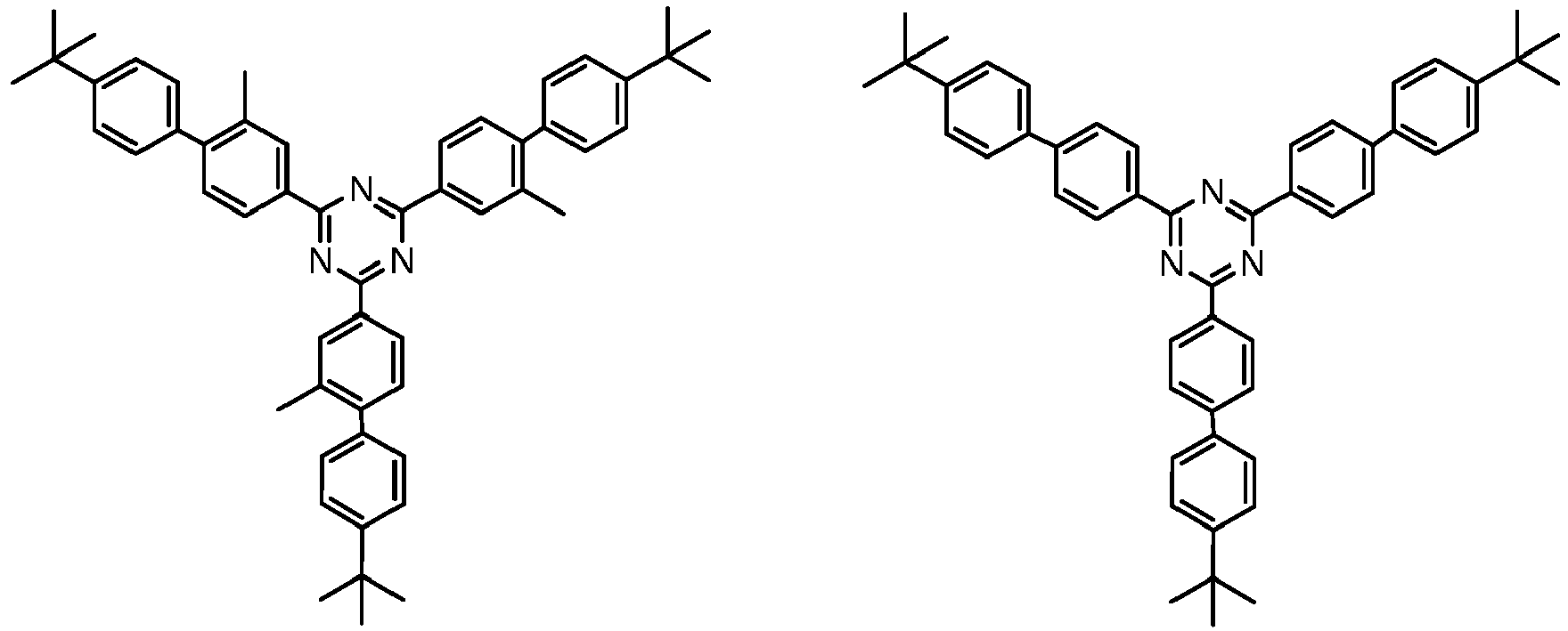

- 13. A composition according to any preceding clause, wherein the at least one solubilizing substituent comprises an amine group which is not directly bonded to the central triazine ring via a nitrogen atom.
- 14. A composition according to clause 3, wherein the triazine repeat unit is provided in a copolymer with a second repeat unit.
- 15. A composition according to clause 14, wherein the second repeat unit is a twisted co-monomer.
- 16. A composition according to any one of clauses 1 to 15, wherein the phosphorescent moiety is provided as a separate chemical entity to the solution processable triazine host material and is blended with the solution processable triazine host material.
- 17. A composition according to any one of clauses 1 to 15, wherein the phosphorescent moiety is chemically bound to the solution processable triazine host material.
- 18. A composition according to clause 17, wherein the phosphorescent moiety is provided in the polymer backbone or in a pendent side chain.
- 19. A composition according to any preceding clause, wherein the phosphorescent moiety is a green emitter.
- 20. A method of fabricating an opto-electrical device, the method comprising the steps: depositing from solution, on a substrate comprising a first electrode for injecting charge carriers of a first polarity, a a composition according to any preceding clause; and depositing thereover a second electrode for injecting charge carriers of a second polarity opposite to the first polarity.
- 21. An opto-electrical device comprising: a substrate; a first electrode disposed over the substrate for injecting charge carriers of a first polarity; a layer disposed over the first electrode comprising a composition according to any one of clauses 1 to 19; and a second electrode disposed thereover for injecting charge carriers of a second polarity opposite to the first polarity.
Claims (15)
- A composition for use in fabricating opto-electrical devices comprising a solution processable triazine host material and a phosphorescent moiety, wherein the triazine host material is an aryl triazine with at least one aryl group having at least one solubilizing substituent bonded thereto, the triazine host material having a solubility of above 8 mg ml-1 in an organic solvent.
- A composition according to claim 1 wherein the triazine host material is a non-polymeric triazine compound.
- A composition according to any preceding claim, wherein the triazine comprises a C4 - C20 alkyl chain solubilising substituent.
- A composition according to any one of the preceding claims, wherein the at least one aryl group is directly bonded to the triazine via a carbon atom, optionally wherein the at least one aryl group is a phenyl ring.
- A composition according to any preceding claim, wherein the triazine compound is a tris-aryl triazine with at least one of the aryl groups, optionally two or three of the aryl groups, having the at least one solubilizing substituent bonded thereto.
- A composition according to any preceding claim, having the formula:


- A composition according to any preceding claim, wherein the at least one solubilizing substituent comprises an amine group which is not directly bonded to the central triazine ring via a nitrogen atom.
- A composition according to any one of claims 1 to 15, wherein the phosphorescent moiety is provided as a separate chemical entity to the solution processable triazine host material and is blended with the solution processable triazine host material.
- A composition according to any preceding claim, wherein the phosphorescent moiety is a green emitter.
- A composition according to any one of the preceding claims wherein the organic solvent is xylene, toluene, chlorobenzene, chloroform or tetrahydrofuran.
- A composition according to any one of the preceding claims wherein the triazine host material has a lower HOMO level than a HOMO level of the phosphorescent moiety.
- A solution comprising a composition according to any one of the preceding claims in an organic solvent.
- A solution according to claim 12 wherein the organic solvent is xylene, toluene, chlorobenzene, chloroform or tetrahydrofuran.
- A method of fabricating an opto-electrical device, the method comprising the steps: depositing from solution, on a substrate comprising a first electrode for injecting charge carriers of a first polarity, a a composition according to any one of claims 1-11; and depositing thereover a second electrode for injecting charge carriers of a second polarity opposite to the first polarity.
- An opto-electrical device comprising: a substrate; a first electrode disposed over the substrate for injecting charge carriers of a first polarity; a layer disposed over the first electrode comprising a composition according to any one of claims 1 to 11; and a second electrode disposed thereover for injecting charge carriers of a second polarity opposite to the first polarity.
Applications Claiming Priority (3)
| Application Number | Priority Date | Filing Date | Title |
|---|---|---|---|
| GBGB0617167.2A GB0617167D0 (en) | 2006-08-31 | 2006-08-31 | Compounds for use in opto-electrical devices |
| EP07804106.8A EP2057249B1 (en) | 2006-08-31 | 2007-08-30 | Compounds for use in opto-electrical devices |
| PCT/GB2007/003300 WO2008025997A1 (en) | 2006-08-31 | 2007-08-30 | Compounds for use in opto-electrical devices |
Related Parent Applications (2)
| Application Number | Title | Priority Date | Filing Date |
|---|---|---|---|
| EP07804106.8A Division EP2057249B1 (en) | 2006-08-31 | 2007-08-30 | Compounds for use in opto-electrical devices |
| EP07804106.8A Division-Into EP2057249B1 (en) | 2006-08-31 | 2007-08-30 | Compounds for use in opto-electrical devices |
Publications (2)
| Publication Number | Publication Date |
|---|---|
| EP3211056A1 true EP3211056A1 (en) | 2017-08-30 |
| EP3211056B1 EP3211056B1 (en) | 2020-07-22 |
Family
ID=37137113
Family Applications (2)
| Application Number | Title | Priority Date | Filing Date |
|---|---|---|---|
| EP17163676.4A Active EP3211056B1 (en) | 2006-08-31 | 2007-08-30 | Compounds for use in opto-electrical devices |
| EP07804106.8A Active EP2057249B1 (en) | 2006-08-31 | 2007-08-30 | Compounds for use in opto-electrical devices |
Family Applications After (1)
| Application Number | Title | Priority Date | Filing Date |
|---|---|---|---|
| EP07804106.8A Active EP2057249B1 (en) | 2006-08-31 | 2007-08-30 | Compounds for use in opto-electrical devices |
Country Status (8)
| Country | Link |
|---|---|
| US (3) | US20100013377A1 (en) |
| EP (2) | EP3211056B1 (en) |
| JP (2) | JP5721948B2 (en) |
| KR (2) | KR20150071010A (en) |
| CN (2) | CN101522857B (en) |
| GB (1) | GB0617167D0 (en) |
| TW (1) | TWI482760B (en) |
| WO (1) | WO2008025997A1 (en) |
Cited By (1)
| Publication number | Priority date | Publication date | Assignee | Title |
|---|---|---|---|---|
| KR20200073993A (en) * | 2018-12-14 | 2020-06-24 | 시노라 게엠베하 | Organic Electroluminescent Devices Comprising Host Compounds |
Families Citing this family (29)
| Publication number | Priority date | Publication date | Assignee | Title |
|---|---|---|---|---|
| JP5556063B2 (en) | 2008-06-23 | 2014-07-23 | 住友化学株式会社 | Composition and light-emitting device using the composition |
| EP2471889A4 (en) * | 2009-08-27 | 2013-06-26 | Sumitomo Chemical Co | METAL COMPLEX COMPOSITION AND COMPLEX POLYMER |
| US9666806B2 (en) | 2009-09-16 | 2017-05-30 | Merck Patent Gmbh | Formulations for the production of electronic devices |
| JP5742160B2 (en) * | 2009-10-19 | 2015-07-01 | 住友化学株式会社 | Metal complex, polymer compound and device using the same |
| US8617720B2 (en) | 2009-12-21 | 2013-12-31 | E I Du Pont De Nemours And Company | Electroactive composition and electronic device made with the composition |
| WO2011137922A1 (en) | 2010-05-03 | 2011-11-10 | Merck Patent Gmbh | Formulations and electronic devices |
| EP2566875B1 (en) * | 2010-05-03 | 2016-01-06 | Merck Patent GmbH | Formulations and electronic devices |
| JP5837051B2 (en) * | 2010-05-03 | 2015-12-24 | メルク パテント ゲーエムベーハー | Formulations and electronic devices |
| GB2484253B (en) | 2010-05-14 | 2013-09-11 | Cambridge Display Tech Ltd | Organic light-emitting composition and device |
| JP5968885B2 (en) * | 2010-07-30 | 2016-08-10 | メルク パテント ゲーエムベーハー | Organic electroluminescence device |
| US9159930B2 (en) | 2010-11-26 | 2015-10-13 | Merck Patent Gmbh | Formulations and electronic devices |
| US20130264561A1 (en) * | 2010-12-20 | 2013-10-10 | E I Du Pont De Nemours And Company | Electroactive compositions for electronic applications |
| JP5727038B2 (en) | 2010-12-20 | 2015-06-03 | イー・アイ・デュポン・ドウ・ヌムール・アンド・カンパニーE.I.Du Pont De Nemours And Company | Compositions for electronic technology applications |
| KR101853013B1 (en) * | 2011-01-17 | 2018-04-30 | 삼성전자주식회사 | Polymer and organic light emitting diode comprising the same |
| GB201107917D0 (en) * | 2011-05-12 | 2011-06-22 | Cambridge Display Tech Ltd | Organic light emitting material and device |
| GB201107905D0 (en) | 2011-05-12 | 2011-06-22 | Cambridge Display Tech Ltd | Light-emitting material, composition and device |
| WO2013005031A1 (en) | 2011-07-04 | 2013-01-10 | Cambridge Display Technology Limited | Organic light emitting device and method |
| CN102382069B (en) * | 2011-08-11 | 2014-04-02 | 大连理工大学 | Monomer preparation method of dihalide and binitro triaryl methyl-1, 3, 5-triazine |
| JP6090317B2 (en) * | 2012-06-19 | 2017-03-08 | 住友化学株式会社 | Polymer compound and light emitting device using the same |
| GB201223283D0 (en) * | 2012-12-21 | 2013-02-06 | Cambridge Display Tech Ltd | Polymer and organic electronic device |
| GB2512021B (en) * | 2012-12-21 | 2015-12-23 | Cambridge Display Tech Ltd | Light-emitting compound |
| KR101829745B1 (en) | 2014-01-24 | 2018-02-19 | 삼성에스디아이 주식회사 | Organic compound and composition and organic optoelectric device and display device |
| CN107592860B (en) | 2015-04-24 | 2020-11-03 | 三星Sdi株式会社 | Organic compounds, compositions and organic photodiodes |
| WO2016170671A1 (en) | 2015-04-24 | 2016-10-27 | 住友化学株式会社 | Light emitting element and composition used in said light emitting element |
| KR101962758B1 (en) * | 2015-06-17 | 2019-03-27 | 삼성에스디아이 주식회사 | Organic compound for optoelectric device and organic optoelectric device and display device |
| CN108264490B (en) * | 2016-12-30 | 2021-06-01 | 湖北尚赛光电材料有限公司 | 1,3, 5-triazine derivative and preparation method and application thereof |
| JP6711808B2 (en) * | 2017-11-21 | 2020-06-17 | 住友化学株式会社 | Light emitting device and composition used for the light emitting device |
| US20210336151A1 (en) * | 2020-04-28 | 2021-10-28 | Semiconductor Energy Laboratory Co., Ltd. | Light-Emitting Device Material, Electron-Transport Layer Material, Organic Compound, Light-Emitting Device, Light-Emitting Apparatus, Electronic Device, and Lighting Device |
| TW202239939A (en) * | 2021-01-28 | 2022-10-16 | 日商半導體能源研究所股份有限公司 | Organic compound, light-emitting device, light-emitting apparatus, electronic device, and lighting device |
Citations (11)
| Publication number | Priority date | Publication date | Assignee | Title |
|---|---|---|---|---|
| US6225467B1 (en) * | 2000-01-21 | 2001-05-01 | Xerox Corporation | Electroluminescent (EL) devices |
| JP2003317946A (en) | 2002-04-23 | 2003-11-07 | Konica Minolta Holdings Inc | Organic EL element and method of manufacturing organic EL element |
| JP2004022334A (en) * | 2002-06-17 | 2004-01-22 | Konica Minolta Holdings Inc | Organic electroluminescence element and display device |
| WO2004062324A1 (en) | 2002-12-27 | 2004-07-22 | Fuji Photo Film Co., Ltd. | Organic electroluminescent device |
| WO2004077885A2 (en) * | 2003-02-28 | 2004-09-10 | Ciba Specialty Chemicals Holding Inc. | Electroluminescent device |
| US6821643B1 (en) * | 2000-01-21 | 2004-11-23 | Xerox Corporation | Electroluminescent (EL) devices |
| EP1610398A2 (en) * | 2004-06-25 | 2005-12-28 | Samsung SDI Co., Ltd. | Organic electroluminescent device |
| JP2006188493A (en) | 2004-12-10 | 2006-07-20 | Pioneer Electronic Corp | Organic compounds, charge transport materials, and organic electroluminescent devices |
| JP2006190759A (en) | 2005-01-05 | 2006-07-20 | Idemitsu Kosan Co Ltd | Organic electroluminescence device |
| JP2006222060A (en) | 2005-01-13 | 2006-08-24 | Seiko Epson Corp | Organic light emitting device manufacturing method, organic light emitting device, electronic device, and electronic apparatus |
| US20090236973A1 (en) | 2004-12-10 | 2009-09-24 | Pioneer Corporation | Organic compound, charge-transporting material, and organic electroluminescent element |
Family Cites Families (71)
| Publication number | Priority date | Publication date | Assignee | Title |
|---|---|---|---|---|
| US4539507A (en) * | 1983-03-25 | 1985-09-03 | Eastman Kodak Company | Organic electroluminescent devices having improved power conversion efficiencies |
| GB8909011D0 (en) | 1989-04-20 | 1989-06-07 | Friend Richard H | Electroluminescent devices |
| US5150006A (en) * | 1991-08-01 | 1992-09-22 | Eastman Kodak Company | Blue emitting internal junction organic electroluminescent device (II) |
| JP3490727B2 (en) * | 1991-11-28 | 2004-01-26 | 三洋電機株式会社 | Electroluminescent device |
| US5723873A (en) * | 1994-03-03 | 1998-03-03 | Yang; Yang | Bilayer composite electrodes for diodes |
| DE69526614T2 (en) * | 1994-09-12 | 2002-09-19 | Motorola, Inc. | Light emitting devices containing organometallic complexes. |
| DE4436773A1 (en) | 1994-10-14 | 1996-04-18 | Hoechst Ag | Conjugated polymers with spirocenters and their use as electroluminescent materials |
| JP3865406B2 (en) | 1995-07-28 | 2007-01-10 | 住友化学株式会社 | 2,7-Aryl-9-substituted fluorene and 9-substituted fluorene oligomers and polymers |
| US5798170A (en) * | 1996-02-29 | 1998-08-25 | Uniax Corporation | Long operating life for polymer light-emitting diodes |
| DE19628719B4 (en) * | 1996-07-17 | 2006-10-05 | Hans-Werner Prof. Dr. Schmidt | Electron-conducting layer in organic, electroluminescent arrangements |
| WO1998005187A1 (en) | 1996-07-29 | 1998-02-05 | Cambridge Display Technology Limited | Electroluminescent devices with electrode protection |
| CN1108730C (en) | 1996-09-04 | 2003-05-14 | 剑桥显示技术有限公司 | Organic light-emitting device with improved cathode |
| JP3899566B2 (en) | 1996-11-25 | 2007-03-28 | セイコーエプソン株式会社 | Manufacturing method of organic EL display device |
| US6452218B1 (en) | 1997-06-10 | 2002-09-17 | Uniax Corporation | Ultra-thin alkaline earth metals as stable electron-injecting electrodes for polymer light emitting diodes |
| GB9718393D0 (en) | 1997-08-29 | 1997-11-05 | Cambridge Display Tech Ltd | Electroluminescent Device |
| GB9805476D0 (en) | 1998-03-13 | 1998-05-13 | Cambridge Display Tech Ltd | Electroluminescent devices |
| KR100697861B1 (en) | 1998-03-13 | 2007-03-22 | 캠브리지 디스플레이 테크놀로지 리미티드 | Electric field light emitting devices |
| JP3784169B2 (en) * | 1998-03-20 | 2006-06-07 | 株式会社小松製作所 | Mobile crushing machine |
| GB2335884A (en) | 1998-04-02 | 1999-10-06 | Cambridge Display Tech Ltd | Flexible substrates for electronic or optoelectronic devices |
| US6268695B1 (en) * | 1998-12-16 | 2001-07-31 | Battelle Memorial Institute | Environmental barrier material for organic light emitting device and method of making |
| US6353083B1 (en) * | 1999-02-04 | 2002-03-05 | The Dow Chemical Company | Fluorene copolymers and devices made therefrom |
| GB9903251D0 (en) | 1999-02-12 | 1999-04-07 | Cambridge Display Tech Ltd | Opto-electric devices |
| JP3310658B1 (en) | 1999-03-05 | 2002-08-05 | ケンブリッジ ディスプレイ テクノロジー リミテッド | Polymer synthesis method |
| GB2348316A (en) | 1999-03-26 | 2000-09-27 | Cambridge Display Tech Ltd | Organic opto-electronic device |
| KR20020066321A (en) | 1999-09-03 | 2002-08-14 | 듀폰 디스플레이즈, 인크. | Encapsulation of organic electronic devices |
| US6413645B1 (en) | 2000-04-20 | 2002-07-02 | Battelle Memorial Institute | Ultrabarrier substrates |
| GB0004541D0 (en) | 2000-02-25 | 2000-04-19 | Cambridge Display Tech Ltd | Luminescent polymer |
| US6939624B2 (en) * | 2000-08-11 | 2005-09-06 | Universal Display Corporation | Organometallic compounds and emission-shifting organic electrophosphorescence |
| JP4344494B2 (en) * | 2000-08-24 | 2009-10-14 | 富士フイルム株式会社 | Light emitting device and novel polymer element |
| IL154960A0 (en) | 2000-10-10 | 2003-10-31 | Du Pont | Polymers having attached luminescent metal complexes and devices made with sych polymers |
| JP4006335B2 (en) * | 2000-11-30 | 2007-11-14 | キヤノン株式会社 | Light emitting element and display device |
| EP1889891B1 (en) * | 2000-11-30 | 2017-11-22 | Canon Kabushiki Kaisha | Luminescence device and display apparatus |
| JP4404473B2 (en) | 2000-12-25 | 2010-01-27 | 富士フイルム株式会社 | Novel nitrogen-containing heterocyclic compounds, light emitting device materials, and light emitting devices using them |
| US6693295B2 (en) * | 2000-12-25 | 2004-02-17 | Fuji Photo Film Co., Ltd. | Indole derivative, material for light-emitting device and light-emitting device using the same |
| EP1366113B1 (en) | 2001-02-20 | 2011-04-13 | Isis Innovation Limited | Metal-containing dendrimers |
| DE10109027A1 (en) | 2001-02-24 | 2002-09-05 | Covion Organic Semiconductors | Rhodium and iridium complexes |
| SG92833A1 (en) | 2001-03-27 | 2002-11-19 | Sumitomo Chemical Co | Polymeric light emitting substance and polymer light emitting device using the same |
| EP1375482A4 (en) | 2001-04-05 | 2005-01-19 | Sankyo Co | Enzamidine derivative |
| GB0109108D0 (en) | 2001-04-11 | 2001-05-30 | Cambridge Display Tech Ltd | Polymer, its preparation and uses |
| JP2004519830A (en) | 2001-04-17 | 2004-07-02 | コーニンクレッカ フィリップス エレクトロニクス エヌ ヴィ | LED with conductive transparent polymer layer containing low sulfate and high metal ions |
| JP2002324679A (en) | 2001-04-26 | 2002-11-08 | Honda Motor Co Ltd | Organic electroluminescence device |
| SG94878A1 (en) | 2001-07-30 | 2003-03-18 | Sumitomo Chemical Co | Polymeric fluorescent substance and polymer light-emitting device using the same |
| JP4574936B2 (en) | 2001-08-31 | 2010-11-04 | 日本放送協会 | Phosphorescent compound and phosphorescent composition |
| US7250226B2 (en) * | 2001-08-31 | 2007-07-31 | Nippon Hoso Kyokai | Phosphorescent compound, a phosphorescent composition and an organic light-emitting device |
| KR100543837B1 (en) * | 2001-09-04 | 2006-01-23 | 캐논 가부시끼가이샤 | Polymer compound and organic light emitting device |
| US6730417B2 (en) * | 2002-01-29 | 2004-05-04 | Xerox Corporation | Organic electroluminescent (EL) devices |
| GB0209652D0 (en) | 2002-04-26 | 2002-06-05 | Univ Cambridge Tech | Solution-processable phosphorescent materials |
| JP4256625B2 (en) * | 2002-05-15 | 2009-04-22 | 富士フイルム株式会社 | Heterocyclic compound and light emitting device using the same |
| US7169482B2 (en) | 2002-07-26 | 2007-01-30 | Lg.Philips Lcd Co., Ltd. | Display device with anthracene and triazine derivatives |
| DE10238903A1 (en) | 2002-08-24 | 2004-03-04 | Covion Organic Semiconductors Gmbh | New heteroaromatic rhodium and iridium complexes, useful in electroluminescent and/or phosphorescent devices as the emission layer and for use in solar cells, photovoltaic devices and organic photodetectors |
| JP4707082B2 (en) * | 2002-11-26 | 2011-06-22 | コニカミノルタホールディングス株式会社 | Organic electroluminescence element and display device |
| US6916902B2 (en) * | 2002-12-19 | 2005-07-12 | Dow Global Technologies Inc. | Tricyclic arylamine containing polymers and electronic devices therefrom |
| CN100493286C (en) | 2003-01-24 | 2009-05-27 | 出光兴产株式会社 | organic electroluminescent element |
| JP4703139B2 (en) | 2003-08-04 | 2011-06-15 | 富士フイルム株式会社 | Organic electroluminescence device |
| JP4780696B2 (en) * | 2003-08-29 | 2011-09-28 | 昭和電工株式会社 | Phosphorescent polymer compound and organic light emitting device using the same |
| KR100990065B1 (en) | 2003-09-24 | 2010-10-26 | 후지필름 가부시키가이샤 | Electroluminescent element |
| DE10356099A1 (en) * | 2003-11-27 | 2005-07-07 | Covion Organic Semiconductors Gmbh | Organic electroluminescent element |
| KR101158144B1 (en) | 2003-12-15 | 2012-06-19 | 이데미쓰 고산 가부시키가이샤 | Material for organic electroluminescent device and organic electroluminescent device using same |
| JP4251453B2 (en) | 2004-02-23 | 2009-04-08 | 日新イオン機器株式会社 | Ion implantation method |
| JP2005268022A (en) * | 2004-03-18 | 2005-09-29 | Fuji Photo Film Co Ltd | Organic electroluminescence device |
| JP2005285410A (en) * | 2004-03-29 | 2005-10-13 | Fuji Photo Film Co Ltd | Organic electroluminescence device |
| KR20070010191A (en) | 2004-04-29 | 2007-01-22 | 시바 스페셜티 케미칼스 홀딩 인크. | Electroluminescent devices |
| KR100603349B1 (en) | 2004-06-17 | 2006-07-20 | 삼성에스디아이 주식회사 | Thin film transistor, method of manufacturing same and flat panel display device having same |
| JP2006086284A (en) * | 2004-09-15 | 2006-03-30 | Tosoh Corp | Electron transport material comprising 1,3,5-triazine derivative |
| JP4802472B2 (en) * | 2004-09-28 | 2011-10-26 | Jsr株式会社 | Arylene ether polymer, polymer composition for organic electroluminescence device, and organic electroluminescence device |
| KR100787423B1 (en) * | 2004-11-05 | 2007-12-26 | 삼성에스디아이 주식회사 | Organic electroluminescent element |
| JP2006140218A (en) | 2004-11-10 | 2006-06-01 | Fuji Photo Film Co Ltd | Organic electroluminescent elemnt |
| JP2006176409A (en) * | 2004-12-20 | 2006-07-06 | Dainippon Printing Co Ltd | ORGANIC COMPOUND AND ORGANIC ELECTROLUMINESCENT DEVICE |
| JP4701818B2 (en) * | 2005-04-28 | 2011-06-15 | Jsr株式会社 | Triazine compound, composition for organic electroluminescence device, and organic electroluminescence device |
| GB2426376B (en) * | 2005-05-19 | 2008-12-03 | Cdt Oxford Ltd | Light-emitting device |
| JP5095948B2 (en) * | 2006-02-22 | 2012-12-12 | 東ソー株式会社 | Terphenylyl-1,3,5-triazine derivative, process for producing the same, and organic electroluminescent device comprising the same |
-
2006
- 2006-08-31 GB GBGB0617167.2A patent/GB0617167D0/en not_active Ceased
-
2007
- 2007-08-30 KR KR1020157008024A patent/KR20150071010A/en not_active Ceased
- 2007-08-30 US US12/439,163 patent/US20100013377A1/en not_active Abandoned
- 2007-08-30 KR KR1020097006304A patent/KR20090047547A/en not_active Ceased
- 2007-08-30 CN CN2007800369137A patent/CN101522857B/en active Active
- 2007-08-30 WO PCT/GB2007/003300 patent/WO2008025997A1/en not_active Ceased
- 2007-08-30 EP EP17163676.4A patent/EP3211056B1/en active Active
- 2007-08-30 CN CN201310247498.7A patent/CN103325962B/en active Active
- 2007-08-30 EP EP07804106.8A patent/EP2057249B1/en active Active
- 2007-08-30 JP JP2009526176A patent/JP5721948B2/en active Active
- 2007-08-31 TW TW096132687A patent/TWI482760B/en active
-
2014
- 2014-07-21 US US14/337,202 patent/US9680110B2/en active Active
-
2015
- 2015-03-25 JP JP2015062158A patent/JP6167126B2/en active Active
- 2015-03-30 US US14/673,752 patent/US20150207081A1/en not_active Abandoned
Patent Citations (13)
| Publication number | Priority date | Publication date | Assignee | Title |
|---|---|---|---|---|
| US6821643B1 (en) * | 2000-01-21 | 2004-11-23 | Xerox Corporation | Electroluminescent (EL) devices |
| US6225467B1 (en) * | 2000-01-21 | 2001-05-01 | Xerox Corporation | Electroluminescent (EL) devices |
| JP2003317946A (en) | 2002-04-23 | 2003-11-07 | Konica Minolta Holdings Inc | Organic EL element and method of manufacturing organic EL element |
| JP2004022334A (en) * | 2002-06-17 | 2004-01-22 | Konica Minolta Holdings Inc | Organic electroluminescence element and display device |
| WO2004062324A1 (en) | 2002-12-27 | 2004-07-22 | Fuji Photo Film Co., Ltd. | Organic electroluminescent device |
| JP2004221063A (en) | 2002-12-27 | 2004-08-05 | Fuji Photo Film Co Ltd | Organic electroluminescence device |
| WO2004077885A2 (en) * | 2003-02-28 | 2004-09-10 | Ciba Specialty Chemicals Holding Inc. | Electroluminescent device |
| EP1610398A2 (en) * | 2004-06-25 | 2005-12-28 | Samsung SDI Co., Ltd. | Organic electroluminescent device |
| JP2006188493A (en) | 2004-12-10 | 2006-07-20 | Pioneer Electronic Corp | Organic compounds, charge transport materials, and organic electroluminescent devices |
| US20090236973A1 (en) | 2004-12-10 | 2009-09-24 | Pioneer Corporation | Organic compound, charge-transporting material, and organic electroluminescent element |
| JP2006190759A (en) | 2005-01-05 | 2006-07-20 | Idemitsu Kosan Co Ltd | Organic electroluminescence device |
| US20080124570A1 (en) | 2005-01-05 | 2008-05-29 | Idemitsu Kosan Co., Ltd. | Organic Electroluminescence Element |
| JP2006222060A (en) | 2005-01-13 | 2006-08-24 | Seiko Epson Corp | Organic light emitting device manufacturing method, organic light emitting device, electronic device, and electronic apparatus |
Non-Patent Citations (2)
| Title |
|---|
| INOMATA H. ET AL: "High efficiency organic electrophosphorescent diodes using 1,3,5-triazine electron transport materials", CHEMISTRY OF MATERIALS, vol. 16, no. 7, 6 April 2004 (2004-04-06), pages 1285 - 1291, XP002508000 |
| T.-Y. CHU ET AL., CHEMICAL PHYSICS LETTERS, vol. 415, no. 1-3, 24 October 2005 (2005-10-24), pages 137 - 140, XP027647415 |
Cited By (1)
| Publication number | Priority date | Publication date | Assignee | Title |
|---|---|---|---|---|
| KR20200073993A (en) * | 2018-12-14 | 2020-06-24 | 시노라 게엠베하 | Organic Electroluminescent Devices Comprising Host Compounds |
Also Published As
| Publication number | Publication date |
|---|---|
| US20140335638A1 (en) | 2014-11-13 |
| US9680110B2 (en) | 2017-06-13 |
| US20100013377A1 (en) | 2010-01-21 |
| KR20090047547A (en) | 2009-05-12 |
| JP5721948B2 (en) | 2015-05-20 |
| TW200823179A (en) | 2008-06-01 |
| CN101522857A (en) | 2009-09-02 |
| TWI482760B (en) | 2015-05-01 |
| JP2015167230A (en) | 2015-09-24 |
| GB0617167D0 (en) | 2006-10-11 |
| CN101522857B (en) | 2013-07-10 |
| WO2008025997A1 (en) | 2008-03-06 |
| JP2010503193A (en) | 2010-01-28 |
| CN103325962B (en) | 2016-12-07 |
| CN103325962A (en) | 2013-09-25 |
| JP6167126B2 (en) | 2017-07-19 |
| EP3211056B1 (en) | 2020-07-22 |
| EP2057249B1 (en) | 2017-11-08 |
| KR20150071010A (en) | 2015-06-25 |
| US20150207081A1 (en) | 2015-07-23 |
| EP2057249A1 (en) | 2009-05-13 |
Similar Documents
| Publication | Publication Date | Title |
|---|---|---|
| EP3211056B1 (en) | Compounds for use in opto-electrical devices | |
| EP2630675B1 (en) | Organic light-emitting device and method | |
| US8981354B2 (en) | Organic light-emitting polymer and device | |
| EP2738195B1 (en) | Polymer and organic electronic device | |
| EP2804927B1 (en) | Monomers, polymers and organic electronic devices | |
| WO2014102543A2 (en) | Polymer and device | |
| US20130075714A1 (en) | Polymer, polymer composition and organic light-emitting device | |
| WO2010119273A1 (en) | Organic electroluminescent device and method of fabrication | |
| EP1969027B1 (en) | Arylamine polymer | |
| EP3295495B1 (en) | Light-emitting compound | |
| WO2006070185A1 (en) | Rigid amines | |
| US10290810B2 (en) | Polymer and organic electronic device | |
| EP2016112B1 (en) | Opto-electrical polymers and devices | |
| EP3259276A1 (en) | Compound, composition and organic light-emitting device | |
| WO2015079261A1 (en) | Polymer and organic light-emitting device |
Legal Events
| Date | Code | Title | Description |
|---|---|---|---|
| PUAI | Public reference made under article 153(3) epc to a published international application that has entered the european phase |
Free format text: ORIGINAL CODE: 0009012 |
|
| STAA | Information on the status of an ep patent application or granted ep patent |
Free format text: STATUS: THE APPLICATION HAS BEEN PUBLISHED |
|
| AC | Divisional application: reference to earlier application |
Ref document number: 2057249 Country of ref document: EP Kind code of ref document: P |
|
| AK | Designated contracting states |
Kind code of ref document: A1 Designated state(s): AT BE BG CH CY CZ DE DK EE ES FI FR GB GR HU IE IS IT LI LT LU LV MC MT NL PL PT RO SE SI SK TR |
|
| RIN1 | Information on inventor provided before grant (corrected) |
Inventor name: MALE, NIGEL Inventor name: PILLOW, JONATHAN |
|
| STAA | Information on the status of an ep patent application or granted ep patent |
Free format text: STATUS: REQUEST FOR EXAMINATION WAS MADE |
|
| TPAC | Observations filed by third parties |
Free format text: ORIGINAL CODE: EPIDOSNTIPA |
|
| 17P | Request for examination filed |
Effective date: 20180228 |
|
| RBV | Designated contracting states (corrected) |
Designated state(s): AT BE BG CH CY CZ DE DK EE ES FI FR GB GR HU IE IS IT LI LT LU LV MC MT NL PL PT RO SE SI SK TR |
|
| STAA | Information on the status of an ep patent application or granted ep patent |
Free format text: STATUS: EXAMINATION IS IN PROGRESS |
|
| 17Q | First examination report despatched |
Effective date: 20180703 |
|
| TPAC | Observations filed by third parties |
Free format text: ORIGINAL CODE: EPIDOSNTIPA |
|
| GRAP | Despatch of communication of intention to grant a patent |
Free format text: ORIGINAL CODE: EPIDOSNIGR1 |
|
| STAA | Information on the status of an ep patent application or granted ep patent |
Free format text: STATUS: GRANT OF PATENT IS INTENDED |
|
| INTG | Intention to grant announced |
Effective date: 20200205 |
|
| GRAS | Grant fee paid |
Free format text: ORIGINAL CODE: EPIDOSNIGR3 |
|
| GRAA | (expected) grant |
Free format text: ORIGINAL CODE: 0009210 |
|
| STAA | Information on the status of an ep patent application or granted ep patent |
Free format text: STATUS: THE PATENT HAS BEEN GRANTED |
|
| AC | Divisional application: reference to earlier application |
Ref document number: 2057249 Country of ref document: EP Kind code of ref document: P |
|
| AK | Designated contracting states |
Kind code of ref document: B1 Designated state(s): AT BE BG CH CY CZ DE DK EE ES FI FR GB GR HU IE IS IT LI LT LU LV MC MT NL PL PT RO SE SI SK TR |
|
| REG | Reference to a national code |
Ref country code: GB Ref legal event code: FG4D |
|
| REG | Reference to a national code |
Ref country code: CH Ref legal event code: EP |
|
| REG | Reference to a national code |
Ref country code: DE Ref legal event code: R096 Ref document number: 602007060488 Country of ref document: DE |
|
| REG | Reference to a national code |
Ref country code: AT Ref legal event code: REF Ref document number: 1293387 Country of ref document: AT Kind code of ref document: T Effective date: 20200815 |
|
| REG | Reference to a national code |
Ref country code: IE Ref legal event code: FG4D |
|
| REG | Reference to a national code |
Ref country code: DE Ref legal event code: R082 Ref document number: 602007060488 Country of ref document: DE Representative=s name: VENNER SHIPLEY GERMANY LLP, DE Ref country code: DE Ref legal event code: R082 Ref document number: 602007060488 Country of ref document: DE Representative=s name: VENNER SHIPLEY LLP, DE |
|
| REG | Reference to a national code |
Ref country code: LT Ref legal event code: MG4D |
|
| REG | Reference to a national code |
Ref country code: AT Ref legal event code: MK05 Ref document number: 1293387 Country of ref document: AT Kind code of ref document: T Effective date: 20200722 |
|
| PG25 | Lapsed in a contracting state [announced via postgrant information from national office to epo] |
Ref country code: LT Free format text: LAPSE BECAUSE OF FAILURE TO SUBMIT A TRANSLATION OF THE DESCRIPTION OR TO PAY THE FEE WITHIN THE PRESCRIBED TIME-LIMIT Effective date: 20200722 Ref country code: FI Free format text: LAPSE BECAUSE OF FAILURE TO SUBMIT A TRANSLATION OF THE DESCRIPTION OR TO PAY THE FEE WITHIN THE PRESCRIBED TIME-LIMIT Effective date: 20200722 Ref country code: PT Free format text: LAPSE BECAUSE OF FAILURE TO SUBMIT A TRANSLATION OF THE DESCRIPTION OR TO PAY THE FEE WITHIN THE PRESCRIBED TIME-LIMIT Effective date: 20201123 Ref country code: SE Free format text: LAPSE BECAUSE OF FAILURE TO SUBMIT A TRANSLATION OF THE DESCRIPTION OR TO PAY THE FEE WITHIN THE PRESCRIBED TIME-LIMIT Effective date: 20200722 Ref country code: GR Free format text: LAPSE BECAUSE OF FAILURE TO SUBMIT A TRANSLATION OF THE DESCRIPTION OR TO PAY THE FEE WITHIN THE PRESCRIBED TIME-LIMIT Effective date: 20201023 Ref country code: ES Free format text: LAPSE BECAUSE OF FAILURE TO SUBMIT A TRANSLATION OF THE DESCRIPTION OR TO PAY THE FEE WITHIN THE PRESCRIBED TIME-LIMIT Effective date: 20200722 Ref country code: BG Free format text: LAPSE BECAUSE OF FAILURE TO SUBMIT A TRANSLATION OF THE DESCRIPTION OR TO PAY THE FEE WITHIN THE PRESCRIBED TIME-LIMIT Effective date: 20201022 Ref country code: AT Free format text: LAPSE BECAUSE OF FAILURE TO SUBMIT A TRANSLATION OF THE DESCRIPTION OR TO PAY THE FEE WITHIN THE PRESCRIBED TIME-LIMIT Effective date: 20200722 |
|
| PG25 | Lapsed in a contracting state [announced via postgrant information from national office to epo] |
Ref country code: PL Free format text: LAPSE BECAUSE OF FAILURE TO SUBMIT A TRANSLATION OF THE DESCRIPTION OR TO PAY THE FEE WITHIN THE PRESCRIBED TIME-LIMIT Effective date: 20200722 Ref country code: LV Free format text: LAPSE BECAUSE OF FAILURE TO SUBMIT A TRANSLATION OF THE DESCRIPTION OR TO PAY THE FEE WITHIN THE PRESCRIBED TIME-LIMIT Effective date: 20200722 Ref country code: IS Free format text: LAPSE BECAUSE OF FAILURE TO SUBMIT A TRANSLATION OF THE DESCRIPTION OR TO PAY THE FEE WITHIN THE PRESCRIBED TIME-LIMIT Effective date: 20201122 |
|
| PG25 | Lapsed in a contracting state [announced via postgrant information from national office to epo] |
Ref country code: NL Free format text: LAPSE BECAUSE OF FAILURE TO SUBMIT A TRANSLATION OF THE DESCRIPTION OR TO PAY THE FEE WITHIN THE PRESCRIBED TIME-LIMIT Effective date: 20200722 |
|
| REG | Reference to a national code |
Ref country code: CH Ref legal event code: PL |
|
| REG | Reference to a national code |
Ref country code: DE Ref legal event code: R097 Ref document number: 602007060488 Country of ref document: DE |
|
| PG25 | Lapsed in a contracting state [announced via postgrant information from national office to epo] |
Ref country code: IT Free format text: LAPSE BECAUSE OF FAILURE TO SUBMIT A TRANSLATION OF THE DESCRIPTION OR TO PAY THE FEE WITHIN THE PRESCRIBED TIME-LIMIT Effective date: 20200722 Ref country code: EE Free format text: LAPSE BECAUSE OF FAILURE TO SUBMIT A TRANSLATION OF THE DESCRIPTION OR TO PAY THE FEE WITHIN THE PRESCRIBED TIME-LIMIT Effective date: 20200722 Ref country code: RO Free format text: LAPSE BECAUSE OF FAILURE TO SUBMIT A TRANSLATION OF THE DESCRIPTION OR TO PAY THE FEE WITHIN THE PRESCRIBED TIME-LIMIT Effective date: 20200722 Ref country code: CZ Free format text: LAPSE BECAUSE OF FAILURE TO SUBMIT A TRANSLATION OF THE DESCRIPTION OR TO PAY THE FEE WITHIN THE PRESCRIBED TIME-LIMIT Effective date: 20200722 Ref country code: DK Free format text: LAPSE BECAUSE OF FAILURE TO SUBMIT A TRANSLATION OF THE DESCRIPTION OR TO PAY THE FEE WITHIN THE PRESCRIBED TIME-LIMIT Effective date: 20200722 Ref country code: CH Free format text: LAPSE BECAUSE OF NON-PAYMENT OF DUE FEES Effective date: 20200831 Ref country code: LI Free format text: LAPSE BECAUSE OF NON-PAYMENT OF DUE FEES Effective date: 20200831 Ref country code: LU Free format text: LAPSE BECAUSE OF NON-PAYMENT OF DUE FEES Effective date: 20200830 |
|
| REG | Reference to a national code |
Ref country code: BE Ref legal event code: MM Effective date: 20200831 |
|
| PLBE | No opposition filed within time limit |
Free format text: ORIGINAL CODE: 0009261 |
|
| STAA | Information on the status of an ep patent application or granted ep patent |
Free format text: STATUS: NO OPPOSITION FILED WITHIN TIME LIMIT |
|
| GBPC | Gb: european patent ceased through non-payment of renewal fee |
Effective date: 20201022 |
|
| 26N | No opposition filed |
Effective date: 20210423 |
|
| PG25 | Lapsed in a contracting state [announced via postgrant information from national office to epo] |
Ref country code: SK Free format text: LAPSE BECAUSE OF FAILURE TO SUBMIT A TRANSLATION OF THE DESCRIPTION OR TO PAY THE FEE WITHIN THE PRESCRIBED TIME-LIMIT Effective date: 20200722 |
|
| PG25 | Lapsed in a contracting state [announced via postgrant information from national office to epo] |
Ref country code: FR Free format text: LAPSE BECAUSE OF NON-PAYMENT OF DUE FEES Effective date: 20200922 |
|
| PG25 | Lapsed in a contracting state [announced via postgrant information from national office to epo] |
Ref country code: BE Free format text: LAPSE BECAUSE OF NON-PAYMENT OF DUE FEES Effective date: 20200831 Ref country code: SI Free format text: LAPSE BECAUSE OF FAILURE TO SUBMIT A TRANSLATION OF THE DESCRIPTION OR TO PAY THE FEE WITHIN THE PRESCRIBED TIME-LIMIT Effective date: 20200722 Ref country code: GB Free format text: LAPSE BECAUSE OF NON-PAYMENT OF DUE FEES Effective date: 20201022 Ref country code: IE Free format text: LAPSE BECAUSE OF NON-PAYMENT OF DUE FEES Effective date: 20200830 |
|
| REG | Reference to a national code |
Ref country code: NL Ref legal event code: MP Effective date: 20200722 |
|
| PG25 | Lapsed in a contracting state [announced via postgrant information from national office to epo] |
Ref country code: TR Free format text: LAPSE BECAUSE OF FAILURE TO SUBMIT A TRANSLATION OF THE DESCRIPTION OR TO PAY THE FEE WITHIN THE PRESCRIBED TIME-LIMIT Effective date: 20200722 Ref country code: MT Free format text: LAPSE BECAUSE OF FAILURE TO SUBMIT A TRANSLATION OF THE DESCRIPTION OR TO PAY THE FEE WITHIN THE PRESCRIBED TIME-LIMIT Effective date: 20200722 Ref country code: CY Free format text: LAPSE BECAUSE OF FAILURE TO SUBMIT A TRANSLATION OF THE DESCRIPTION OR TO PAY THE FEE WITHIN THE PRESCRIBED TIME-LIMIT Effective date: 20200722 |
|
| PG25 | Lapsed in a contracting state [announced via postgrant information from national office to epo] |
Ref country code: MC Free format text: LAPSE BECAUSE OF FAILURE TO SUBMIT A TRANSLATION OF THE DESCRIPTION OR TO PAY THE FEE WITHIN THE PRESCRIBED TIME-LIMIT Effective date: 20200722 |
|
| PGFP | Annual fee paid to national office [announced via postgrant information from national office to epo] |
Ref country code: DE Payment date: 20250827 Year of fee payment: 19 |