EP1385221A2 - Display device with anthracene and triazine derivtives - Google Patents
Display device with anthracene and triazine derivtives Download PDFInfo
- Publication number
- EP1385221A2 EP1385221A2 EP03254473A EP03254473A EP1385221A2 EP 1385221 A2 EP1385221 A2 EP 1385221A2 EP 03254473 A EP03254473 A EP 03254473A EP 03254473 A EP03254473 A EP 03254473A EP 1385221 A2 EP1385221 A2 EP 1385221A2
- Authority
- EP
- European Patent Office
- Prior art keywords
- group
- carbon atoms
- derivative compound
- anthracene
- anthracene derivative
- Prior art date
- Legal status (The legal status is an assumption and is not a legal conclusion. Google has not performed a legal analysis and makes no representation as to the accuracy of the status listed.)
- Granted
Links
- JIHQDMXYYFUGFV-UHFFFAOYSA-N c1ncncn1 Chemical compound c1ncncn1 JIHQDMXYYFUGFV-UHFFFAOYSA-N 0.000 description 1
Images


Classifications
-
- H—ELECTRICITY
- H05—ELECTRIC TECHNIQUES NOT OTHERWISE PROVIDED FOR
- H05B—ELECTRIC HEATING; ELECTRIC LIGHT SOURCES NOT OTHERWISE PROVIDED FOR; CIRCUIT ARRANGEMENTS FOR ELECTRIC LIGHT SOURCES, IN GENERAL
- H05B33/00—Electroluminescent light sources
- H05B33/12—Light sources with substantially two-dimensional [2D] radiating surfaces
- H05B33/14—Light sources with substantially two-dimensional [2D] radiating surfaces characterised by the chemical or physical composition or the arrangement of the electroluminescent material, or by the simultaneous addition of the electroluminescent material in or onto the light source
-
- C—CHEMISTRY; METALLURGY
- C07—ORGANIC CHEMISTRY
- C07D—HETEROCYCLIC COMPOUNDS
- C07D219/00—Heterocyclic compounds containing acridine or hydrogenated acridine ring systems
- C07D219/04—Heterocyclic compounds containing acridine or hydrogenated acridine ring systems with hetero atoms or with carbon atoms having three bonds to hetero atoms with at the most one bond to halogen, e.g. ester or nitrile radicals, directly attached to carbon atoms of the ring system
- C07D219/06—Oxygen atoms
-
- C—CHEMISTRY; METALLURGY
- C07—ORGANIC CHEMISTRY
- C07D—HETEROCYCLIC COMPOUNDS
- C07D251/00—Heterocyclic compounds containing 1,3,5-triazine rings
- C07D251/02—Heterocyclic compounds containing 1,3,5-triazine rings not condensed with other rings
- C07D251/12—Heterocyclic compounds containing 1,3,5-triazine rings not condensed with other rings having three double bonds between ring members or between ring members and non-ring members
- C07D251/14—Heterocyclic compounds containing 1,3,5-triazine rings not condensed with other rings having three double bonds between ring members or between ring members and non-ring members with hydrogen or carbon atoms directly attached to at least one ring carbon atom
- C07D251/24—Heterocyclic compounds containing 1,3,5-triazine rings not condensed with other rings having three double bonds between ring members or between ring members and non-ring members with hydrogen or carbon atoms directly attached to at least one ring carbon atom to three ring carbon atoms
-
- C—CHEMISTRY; METALLURGY
- C09—DYES; PAINTS; POLISHES; NATURAL RESINS; ADHESIVES; COMPOSITIONS NOT OTHERWISE PROVIDED FOR; APPLICATIONS OF MATERIALS NOT OTHERWISE PROVIDED FOR
- C09K—MATERIALS FOR MISCELLANEOUS APPLICATIONS, NOT PROVIDED FOR ELSEWHERE
- C09K11/00—Luminescent materials, e.g. electroluminescent or chemiluminescent
- C09K11/06—Luminescent materials, e.g. electroluminescent or chemiluminescent containing organic luminescent materials
-
- H—ELECTRICITY
- H10—SEMICONDUCTOR DEVICES; ELECTRIC SOLID-STATE DEVICES NOT OTHERWISE PROVIDED FOR
- H10K—ORGANIC ELECTRIC SOLID-STATE DEVICES
- H10K50/00—Organic light-emitting devices
- H10K50/10—OLEDs or polymer light-emitting diodes [PLED]
- H10K50/14—Carrier transporting layers
- H10K50/16—Electron transporting layers
-
- H—ELECTRICITY
- H10—SEMICONDUCTOR DEVICES; ELECTRIC SOLID-STATE DEVICES NOT OTHERWISE PROVIDED FOR
- H10K—ORGANIC ELECTRIC SOLID-STATE DEVICES
- H10K50/00—Organic light-emitting devices
- H10K50/10—OLEDs or polymer light-emitting diodes [PLED]
- H10K50/14—Carrier transporting layers
- H10K50/16—Electron transporting layers
- H10K50/166—Electron transporting layers comprising a multilayered structure
-
- H—ELECTRICITY
- H10—SEMICONDUCTOR DEVICES; ELECTRIC SOLID-STATE DEVICES NOT OTHERWISE PROVIDED FOR
- H10K—ORGANIC ELECTRIC SOLID-STATE DEVICES
- H10K85/00—Organic materials used in the body or electrodes of devices covered by this subclass
- H10K85/60—Organic compounds having low molecular weight
- H10K85/615—Polycyclic condensed aromatic hydrocarbons, e.g. anthracene
-
- H—ELECTRICITY
- H10—SEMICONDUCTOR DEVICES; ELECTRIC SOLID-STATE DEVICES NOT OTHERWISE PROVIDED FOR
- H10K—ORGANIC ELECTRIC SOLID-STATE DEVICES
- H10K85/00—Organic materials used in the body or electrodes of devices covered by this subclass
- H10K85/60—Organic compounds having low molecular weight
- H10K85/615—Polycyclic condensed aromatic hydrocarbons, e.g. anthracene
- H10K85/626—Polycyclic condensed aromatic hydrocarbons, e.g. anthracene containing more than one polycyclic condensed aromatic rings, e.g. bis-anthracene
-
- H—ELECTRICITY
- H10—SEMICONDUCTOR DEVICES; ELECTRIC SOLID-STATE DEVICES NOT OTHERWISE PROVIDED FOR
- H10K—ORGANIC ELECTRIC SOLID-STATE DEVICES
- H10K85/00—Organic materials used in the body or electrodes of devices covered by this subclass
- H10K85/60—Organic compounds having low molecular weight
- H10K85/649—Aromatic compounds comprising a hetero atom
- H10K85/654—Aromatic compounds comprising a hetero atom comprising only nitrogen as heteroatom
-
- C—CHEMISTRY; METALLURGY
- C09—DYES; PAINTS; POLISHES; NATURAL RESINS; ADHESIVES; COMPOSITIONS NOT OTHERWISE PROVIDED FOR; APPLICATIONS OF MATERIALS NOT OTHERWISE PROVIDED FOR
- C09K—MATERIALS FOR MISCELLANEOUS APPLICATIONS, NOT PROVIDED FOR ELSEWHERE
- C09K2211/00—Chemical nature of organic luminescent or tenebrescent compounds
- C09K2211/10—Non-macromolecular compounds
- C09K2211/1003—Carbocyclic compounds
- C09K2211/1011—Condensed systems
-
- C—CHEMISTRY; METALLURGY
- C09—DYES; PAINTS; POLISHES; NATURAL RESINS; ADHESIVES; COMPOSITIONS NOT OTHERWISE PROVIDED FOR; APPLICATIONS OF MATERIALS NOT OTHERWISE PROVIDED FOR
- C09K—MATERIALS FOR MISCELLANEOUS APPLICATIONS, NOT PROVIDED FOR ELSEWHERE
- C09K2211/00—Chemical nature of organic luminescent or tenebrescent compounds
- C09K2211/10—Non-macromolecular compounds
- C09K2211/1018—Heterocyclic compounds
- C09K2211/1025—Heterocyclic compounds characterised by ligands
- C09K2211/1059—Heterocyclic compounds characterised by ligands containing three nitrogen atoms as heteroatoms
-
- H—ELECTRICITY
- H10—SEMICONDUCTOR DEVICES; ELECTRIC SOLID-STATE DEVICES NOT OTHERWISE PROVIDED FOR
- H10K—ORGANIC ELECTRIC SOLID-STATE DEVICES
- H10K2102/00—Constructional details relating to the organic devices covered by this subclass
- H10K2102/10—Transparent electrodes, e.g. using graphene
- H10K2102/101—Transparent electrodes, e.g. using graphene comprising transparent conductive oxides [TCO]
- H10K2102/103—Transparent electrodes, e.g. using graphene comprising transparent conductive oxides [TCO] comprising indium oxides, e.g. ITO
-
- H—ELECTRICITY
- H10—SEMICONDUCTOR DEVICES; ELECTRIC SOLID-STATE DEVICES NOT OTHERWISE PROVIDED FOR
- H10K—ORGANIC ELECTRIC SOLID-STATE DEVICES
- H10K30/00—Organic devices sensitive to infrared radiation, light, electromagnetic radiation of shorter wavelength or corpuscular radiation
- H10K30/80—Constructional details
- H10K30/865—Intermediate layers comprising a mixture of materials of the adjoining active layers
-
- H—ELECTRICITY
- H10—SEMICONDUCTOR DEVICES; ELECTRIC SOLID-STATE DEVICES NOT OTHERWISE PROVIDED FOR
- H10K—ORGANIC ELECTRIC SOLID-STATE DEVICES
- H10K50/00—Organic light-emitting devices
-
- H—ELECTRICITY
- H10—SEMICONDUCTOR DEVICES; ELECTRIC SOLID-STATE DEVICES NOT OTHERWISE PROVIDED FOR
- H10K—ORGANIC ELECTRIC SOLID-STATE DEVICES
- H10K85/00—Organic materials used in the body or electrodes of devices covered by this subclass
- H10K85/30—Coordination compounds
- H10K85/311—Phthalocyanine
-
- H—ELECTRICITY
- H10—SEMICONDUCTOR DEVICES; ELECTRIC SOLID-STATE DEVICES NOT OTHERWISE PROVIDED FOR
- H10K—ORGANIC ELECTRIC SOLID-STATE DEVICES
- H10K85/00—Organic materials used in the body or electrodes of devices covered by this subclass
- H10K85/30—Coordination compounds
- H10K85/321—Metal complexes comprising a group IIIA element, e.g. Tris (8-hydroxyquinoline) gallium [Gaq3]
- H10K85/324—Metal complexes comprising a group IIIA element, e.g. Tris (8-hydroxyquinoline) gallium [Gaq3] comprising aluminium, e.g. Alq3
-
- H—ELECTRICITY
- H10—SEMICONDUCTOR DEVICES; ELECTRIC SOLID-STATE DEVICES NOT OTHERWISE PROVIDED FOR
- H10K—ORGANIC ELECTRIC SOLID-STATE DEVICES
- H10K85/00—Organic materials used in the body or electrodes of devices covered by this subclass
- H10K85/60—Organic compounds having low molecular weight
- H10K85/631—Amine compounds having at least two aryl rest on at least one amine-nitrogen atom, e.g. triphenylamine
-
- H—ELECTRICITY
- H10—SEMICONDUCTOR DEVICES; ELECTRIC SOLID-STATE DEVICES NOT OTHERWISE PROVIDED FOR
- H10K—ORGANIC ELECTRIC SOLID-STATE DEVICES
- H10K85/00—Organic materials used in the body or electrodes of devices covered by this subclass
- H10K85/60—Organic compounds having low molecular weight
- H10K85/631—Amine compounds having at least two aryl rest on at least one amine-nitrogen atom, e.g. triphenylamine
- H10K85/633—Amine compounds having at least two aryl rest on at least one amine-nitrogen atom, e.g. triphenylamine comprising polycyclic condensed aromatic hydrocarbons as substituents on the nitrogen atom
-
- H—ELECTRICITY
- H10—SEMICONDUCTOR DEVICES; ELECTRIC SOLID-STATE DEVICES NOT OTHERWISE PROVIDED FOR
- H10K—ORGANIC ELECTRIC SOLID-STATE DEVICES
- H10K85/00—Organic materials used in the body or electrodes of devices covered by this subclass
- H10K85/60—Organic compounds having low molecular weight
- H10K85/649—Aromatic compounds comprising a hetero atom
- H10K85/657—Polycyclic condensed heteroaromatic hydrocarbons
-
- Y—GENERAL TAGGING OF NEW TECHNOLOGICAL DEVELOPMENTS; GENERAL TAGGING OF CROSS-SECTIONAL TECHNOLOGIES SPANNING OVER SEVERAL SECTIONS OF THE IPC; TECHNICAL SUBJECTS COVERED BY FORMER USPC CROSS-REFERENCE ART COLLECTIONS [XRACs] AND DIGESTS
- Y10—TECHNICAL SUBJECTS COVERED BY FORMER USPC
- Y10S—TECHNICAL SUBJECTS COVERED BY FORMER USPC CROSS-REFERENCE ART COLLECTIONS [XRACs] AND DIGESTS
- Y10S428/00—Stock material or miscellaneous articles
- Y10S428/917—Electroluminescent
Definitions
- OLEDs Organic light emitting devices
- the present invention is accomplished in embodiments by providing a device comprising:
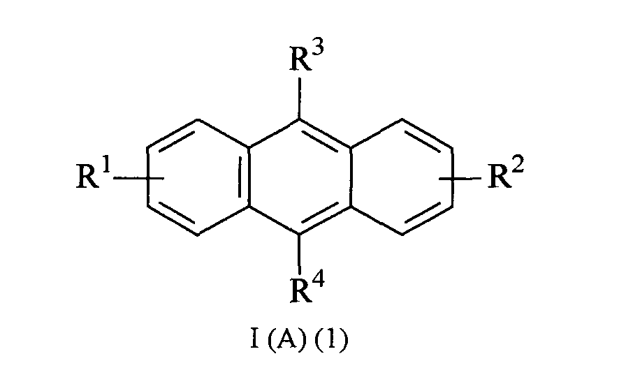
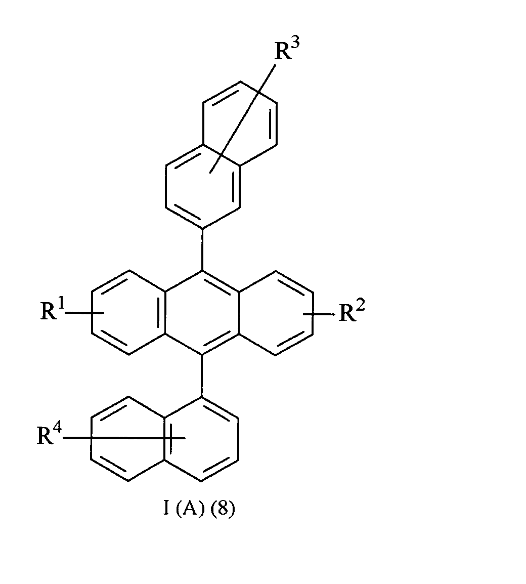
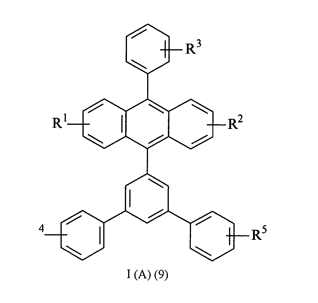
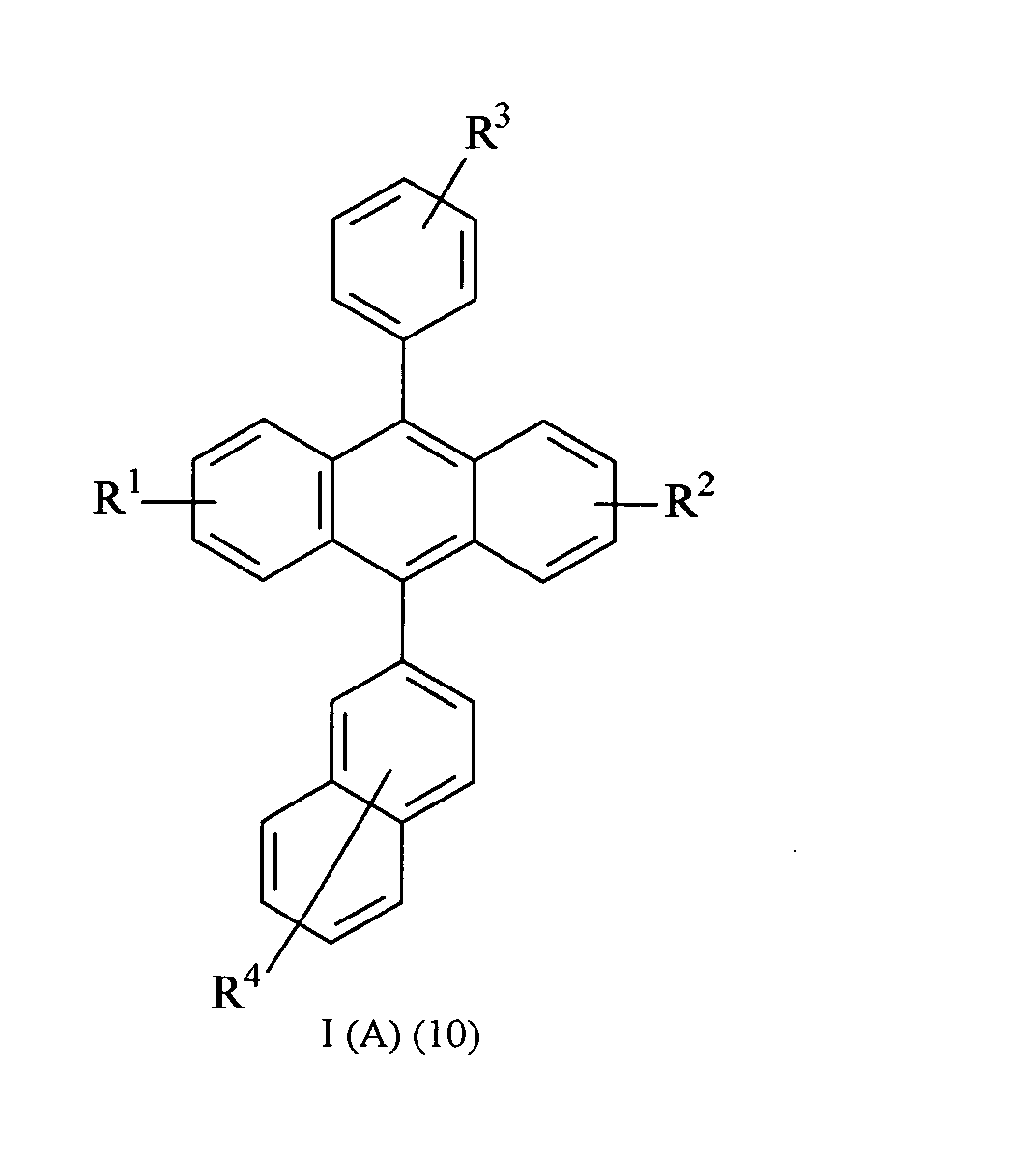
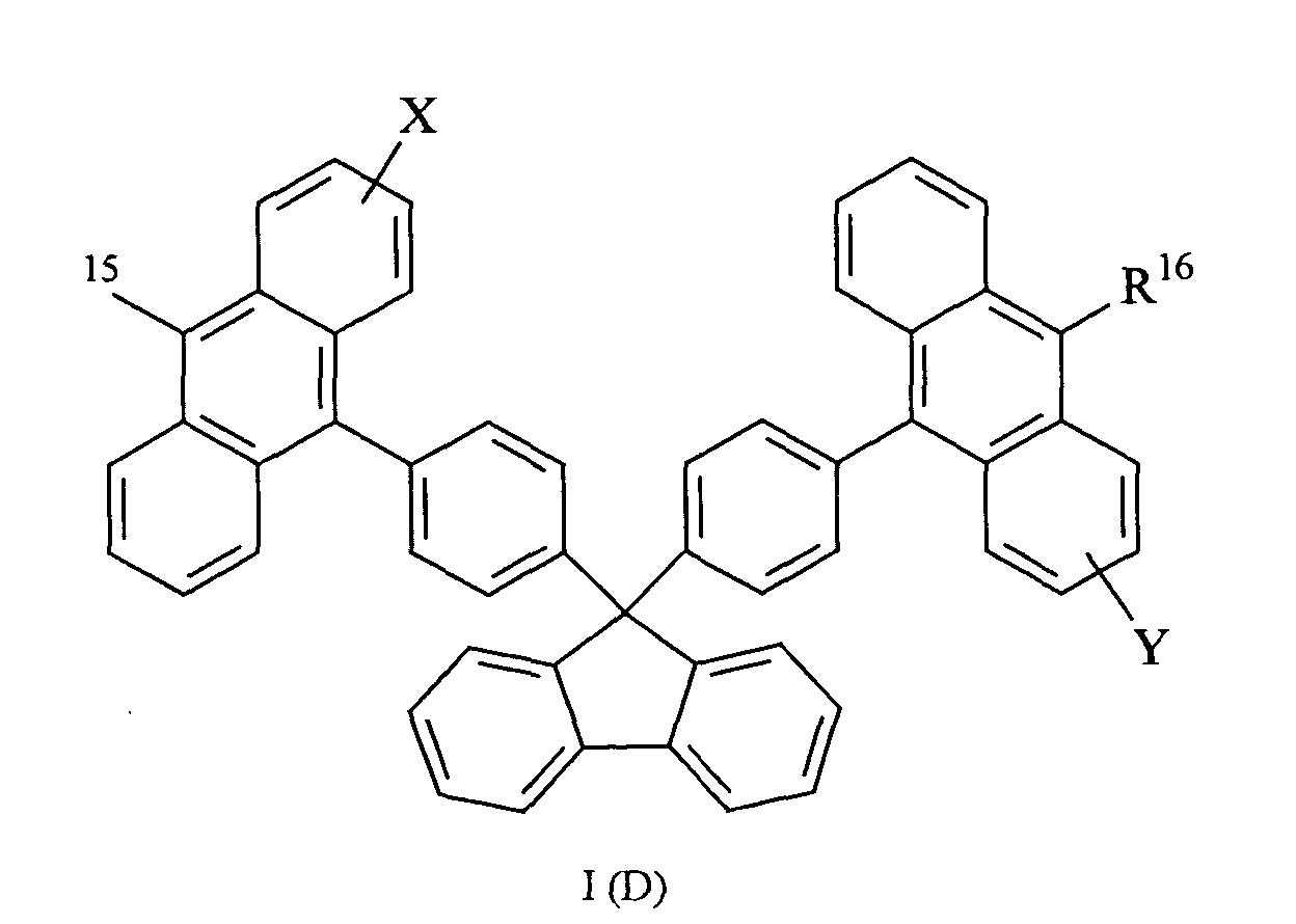
- anthracene derivative compound is selected from the group consisting of formulas I(A)(1) through I(A)(11), formula I(B), formula I(C), and formula I(D)
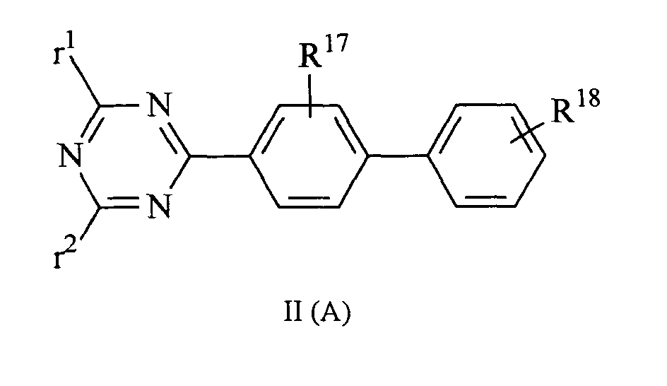
- the triazine derivative compound is selected from the group consisting of formulas II(A), II(B), II(C), and II(D) wherein the formulas and substituents are discussed herein.
- the present organic light emitting device includes within the luminescent region at least one anthracene derivative compound and at least one triazine derivative compound. Any suitable layer sequence and layer composition may be employed to accomplish the present invention.
- FIG. 1 A first exemplary embodiment is seen in FIG. 1 where the OLED 110 is composed of in the depicted sequence: an anode 120; a luminescent region 130; and a cathode 140.
- a second exemplary embodiment is seen in FIG. 2 where the OLED 210 is composed of in the depicted sequence: a first electrode 220; a luminescent region 230 composed of a light emitting zone 230B and a charge transport zone 230A; and a second electrode 240.
- the first electrode can be the cathode while the second electrode is the anode; alternatively, the first electrode can be the anode while the second electrode is the cathode.
- the charge transport zone can be a hole transport zone when the second electrode is the anode; alternatively, the charge transport zone can be an electron transport zone when the second electrode is the cathode.
- FIG. 3 A third exemplary embodiment is seen in FIG. 3 where the OLED 310 is composed of in the depicted sequence: an anode 320; an optional buffer layer 322; a luminescent region 330 composed of a hole transport zone 330A, a light emitting zone 330B, and an electron transport zone 330C; and a cathode 340.
- a substrate is not depicted in FIGS. 1-3; it is understood however that a substrate may be positioned at any suitable place in the depicted OLEDs such as in contact with either electrode.
- the at least one triazine derivative compound may be present as one, two, three or more compounds. Where two or more triazine derivative compounds are present, they may be in a mixture of equal or unequal ratios; or the triazine derivative compounds may be in an unmixed state such as separately disposed in different layers or in different areas of a single layer. In embodiments, the at least one triazine derivative compound may be considered an electron transport material because the transport of electrons is greater than the transport of holes through the triazine derivative compound.
- a number of the triazine derivative compounds in addition to being electron transporters, may also be a blue emitter, i.e., a material wherein holes and electrons can combine to result in the emission of light in the blue region of the visible spectrum.
- the at least one anthracene derivative compound may be present as one, two, three or more compounds. Where two or more anthracene derivative compounds are present, they may be in a mixture of equal or unequal ratios; or the anthracene derivative compounds may be in an unmixed state such as separately disposed in different layers or in different areas of a single layer.
- the at least one anthracene derivative compound is a type of an organic electroluminescent material that may be considered a blue emitter, i.e., a material wherein holes and electrons can combine to result in the emission of light in the blue region of the visible spectrum.
- a number of the anthracene derivative compounds may also be able to transport holes, electrons, or both holes and electrons at a poor, fair, good, or excellent level. Since in embodiments the anthracene derivative compounds may be both a blue emitter and a charge conductor, this dual property allows a degree of flexibility in placement of the anthracene derivative compounds in the OLEDs.
- the at least one anthracene derivative compound and the at least one triazine derivative compound may be present in one, two or more layers, zones, or regions of the instant OLEDs such as the following exemplary OLED configurations (where two or more anthracene derivative compounds are present in the OLED, such anthracene derivative compounds may be the same or different from one another; and where two or more triazine derivative compounds are present in the OLED, such triazine derivative compounds may be the same or different from one another):
- the layer of anthracene derivative compound + triazine derivative compound can be equally viewed as being part of the light emitting zone.
- the configurations can optionally further include a hole transport zone (adjacent the anode) which may comprise an anthracene derivative compound and/or a non-anthracene and non-triazine derivative compound.
- a hole transport zone adjacent the anode which may comprise an anthracene derivative compound and/or a non-anthracene and non-triazine derivative compound.
- the configurations can optionally further include in the hole transport zone (adjacent the anode) a non-anthracene and non-triazine derivative compound.
- the luminescent region including the anthracene derivative compound and the triazine derivative compound can be one, two, three or more layers.
- the anthracene derivative compound and the triazine derivative compound can be deposited with varying concentrations across the thickness of the layer such that two functional areas are produced: a light emitting zone (e.g., anthracene derivative compound + triazine derivative compound) and an electron transport zone (e.g., anthracene derivative compound + triazine derivative compound), where the concentration of the anthracene derivative compound in the electron transport zone is for example less than that in the light emitting zone, or, optionally, even completely absent from the electron transport zone.
- a light emitting zone e.g., anthracene derivative compound + triazine derivative compound
- an electron transport zone e.g., anthracene derivative compound + triazine derivative compound
- a single layer luminescent composed of a mixture of an anthracene derivative compound and a triazine derivative compound, with a constant concentration throughout.
- a multi-layer luminescent region can be composed for example of the following: a light emitting layer in contact with a charge transport layer; and a light emitting layer between a hole transport layer and an electron transport layer.
- the light emitting zone can include a single anthracene derivative compound, or a mixture of two or more anthracene derivative compounds. Where a mixture of two or more anthracene derivative compounds are used, the anthracene derivative compounds may be present in any suitable ratio by weight such as equal or unequal amounts; one compound in the mixture may be present for instance in an amount ranging from 0.1% to 99.9% by weight, the balance being the other compound(s).
- a charge transport material may be present in the light emitting zone at a concentration ranging for example from 0% to about 95% by weight based on the light emitting zone, the balance being the anthracene derivative compound(s) at a concentration ranging from 100% to about 5% by weight based on the light emitting zone.
- the light emitting zone can include a single triazine derivative compound, or a mixture of two or more triazine derivative compounds.
- the triazine derivative compounds may be present in any suitable ratio by weight such as equal or unequal amounts; one compound in the mixture may be present for instance in an amount ranging from 0.1% to 99.9% by weight, the balance being the other compound(s).
- a charge transport material may be present in the light emitting zone at a concentration ranging for example from 0% to about 95% by weight based on the light emitting zone, the balance being the triazine derivative compound(s) at a concentration ranging from 100% to about 5% by weight based on the light emitting zone.
- the light emitting zone can include a mixture of anthracene derivative compound(s) and triazine derivative compound(s).
- each of the anthracene derivative compound(s) and the triazine derivative compound(s) may be present in any suitable ratio by weight such as equal or unequal amounts; one compound in the mixture may be present for instance in an amount ranging from 0.1% to 99.9% by weight, the balance being the other compound(s).
- a charge transport material may be present in the light emitting zone at a concentration ranging for example from 0% to about 95% by weight based on the light emitting zone, the balance being the anthracene derivative compound(s) and the triazine derivative compound(s) at a concentration ranging from 100% to about 5% by weight based on the light emitting zone.
- the light emitting zone can include one or more non-anthracene and non-triazine derivative compounds in any suitable ratio by weight such as equal or unequal amounts. These one or more non-anthracene and non-triazine derivative compounds may be added to the light emitting zone to affect the color intensity or color purity of the emitted light as compared to a light emitting zone without such one or more non-anthracene and non-triazine derivative compounds.
- blue emitting OLEDs are produced; in other embodiments, OLEDs emitting another color may be produced by the use of appropriate materials in the luminescent region such as by adding one or more non-anthracene and non-triazine derivative compounds to the light emitting zone to change the blue color to another color.
- the charge transport zone (whether a hole transport zone or an electron transport zone) includes a single charge transport material or a mixture of two or more charge transport materials at any suitable ratio by weight such as equal or unequal amounts; one compound in the mixture may be present for instance in an amount ranging from 0.1% to 99.9% by weight, the balance being the other compound(s).
- the charge transport zone can include one or more anthracene derivative compound(s), one or more triazine derivative compound(s), one or more non-anthracene and non-triazine compound(s), or any mixture thereof.
- the layers of the OLED may be transparent or opaque depending on the side of the OLED that is facing the viewer. Illustrative materials will now be discussed in constructing OLEDs of the present invention.
- a substantially transparent substrate can comprise various suitable materials including, for example, polymeric components, glass, quartz and the like.
- suitable polymeric components include, but are not limited to polyesters such as MYLAR®, polycarbonates, polyacrylates, polymethacrylates, polysulfones, and the like.
- Other substrate materials can also be selected.
- the substrate may have a thickness of from about 10 to about 5,000 micrometers, and more particularly from about 25 to about 1,000 micrometers.
- An anode can comprise suitable positive charge injecting materials such as indium tin oxide (ITO), silicon, tin oxide, and metals with a work function ranging from about 4 eV to about 6 eV such as gold, platinum, and palladium.
- suitable materials for the anode include, but are not limited to, electrically conductive carbon, ⁇ -conjugated polymers such as polyaniline, polythiophene, polypyrrole, and the like having, for example, a work function equal to, or greater than, about 4 eV, and particularly from about 4 eV to about 6 eV.
- a substantially transparent anode can comprise, for example, indium tin oxide (ITO), very thin substantially transparent metallic layers, comprising a metal with a work function ranging from about 4 eV to about 6 eV such as gold, palladium and the like, having a thickness, for example, from about 10 ⁇ to about 200 ⁇ , and, particularly, from about 30 ⁇ to about 100 ⁇ .
- the thickness of the anode can range from about 10 ⁇ to about 50,000 ⁇ , with the preferred range depending on the electrical and optical constants of the anode material.
- One illustrative range of anode thickness is from about 300 ⁇ to about 3,000 ⁇ .
- a cathode can comprise suitable electron injecting materials, such as metals, including high work function components, such as metals with, for example, a work function from about 4 eV to about 6 eV, or low work function components, such as metals with, for example, a work function of from about 2 eV to about 4 eV.
- the cathode can comprise a combination of a low work function (less than about 4 eV) metal and at least one other metal. Effective proportions of the low work function metal to the second or other metal are from less than about 0.1 weight percent to about 99.9 weight percent.
- low work function metals include, but are not limited to, alkaline metals such as lithium or sodium; Group 2A or alkaline earth metals such as beryllium, magnesium, calcium or barium; and Group III metals including rare earth metals and the actinide group metals such as scandium, yttrium, lanthanum, cerium, europium, terbium or actinium. Lithium, magnesium and calcium are preferred low work function metals.
- the Mg-Ag alloy cathodes are in embodiments preferred cathode materials for forming the cathodes.
- Other specific cathodes comprises a metal-organic mixed later (MOML).
- the cathodes can be formed from lithium alloys with other high work function metals such as aluminum and indium.
- a substantially transparent cathode can comprise very thin substantially transparent metallic layers comprising a metal with a work function ranging from about 2 eV to about 4 eV, such as Mg, Ag, Al, Ca, In, Li and their alloys such as Mg:Ag alloys, comprised of, for example, from about 80 to 95 volume percent of Mg and about 20 to about 5 volume percent of Ag, and Li:Al alloys, comprised of, for example, from about 90 to 99 volume percent of Al, and from about 10 to about 1 volume percent of Li, and the like, having a thickness, for example, from about 10 ⁇ to about 200 ⁇ , and, particularly, from about 30 ⁇ to about 100 ⁇ .
- a metal with a work function ranging from about 2 eV to about 4 eV such as Mg, Ag, Al, Ca, In, Li and their alloys such as Mg:Ag alloys, comprised of, for example, from about 80 to 95 volume percent of Mg and about 20 to about 5 volume percent of Ag, and Li:
- the thickness of the cathode can range from, for example, about 10 nanometers to about 1,000 nanometers.
- the anode and cathode used in the present OLEDs each may be a single layer or may comprise two, three or more layers.
- the electrode may be composed of a charge injection layer (i.e., an electron injection layer or a hole injection layer) and a capping layer. In embodiments, however, the charge injection layer may be considered distinct from the electrode.
- An electron injecting layer can include very thin substantially transparent metallic layers, composed of a metal with a work function ranging from about 2 eV to about 4 eV, such as Mg, Ag, Al, Ca, In, Li and their alloys such as Mg:Ag alloys composed of, for example, from about 80 to 95 volume percent of Mg and about 20 to about 5 volume percent of Ag, and Li:Al alloys, composed of, for example, from about 90 to 99 volume percent of Al, and from about 10 to about 1 volume percent of Li, and the like, having a thickness, for example, from about 10 ⁇ to about 200 ⁇ , and, particularly, from about 30 ⁇ to about 100 ⁇ .
- a metal with a work function ranging from about 2 eV to about 4 eV such as Mg, Ag, Al, Ca, In
- Li and their alloys such as Mg:Ag alloys composed of, for example, from about 80 to 95 volume percent of Mg and about 20 to about 5 volume percent of Ag, and Li:Al alloys,
- the electron injection layer can also include very thin insulative materials such as an oxide material or an alkaline metal compound as described in U.S. Patents 5,457,565; 5,608,287 and 5,739,635.
- a hole injecting layer can be composed of suitable positive charge injecting materials such as indium tin oxide (ITO), silicon, tin oxide, and metals with a work function ranging from about 4 eV to about 6 eV, such as, gold, platinum, and palladium.
- suitable materials for the hole injecting layer include, but are not limited to, electrically conductive carbon, ⁇ -conjugated polymers such as polyaniline, polythiophene, polypyrrole, and the like having, for example, a work function equal to, or greater than, about 4 eV, and particularly from about 4 eV to about 6 eV.
- a substantially transparent hole injecting material can be composed of very thin substantially transparent metallic layers, comprising a metal with a work function ranging from about 4 eV to about 6 eV, such as gold, palladium and the like, having a thickness, for example, from about 10 ⁇ to about 200 ⁇ , and, particularly, from about 30 ⁇ to about 100 ⁇ . Additional suitable forms of hole injecting layers are disclosed in U.S. Patents 4,885,211 and 5,703,436.
- a capping layer on the anode and/or cathode can be included in order to increase the thermal stability, increase the environmental stability, and/or in some other way improve the performance of the organic light emitting device.
- An example of a capping layer that can be used to increase the thermal stability of the organic light emitting is a layer comprised of SiO, SiO 2 , or mixtures thereof.
- An example of a capping layer that can be used to increase the environmental stability of the organic light emitting device is a layer comprised of a stable metal such as Ag, Al, In, or Au.
- Another example of a capping layer that can be used to increase the environmental stability of the organic light emitting device is a layer comprised of a low work function metal as described for example in US Patent No. 5,059,861.
- the thickness of the capping layer can, for example, range from about 20 nanometers to about 5,000 nanometers or from about 50 nanometers to 500 nanometers.
- a buffer layer can be composed of a material with certain hole injection and transport properties and selected such that device performance is improved.
- Suitable materials that can be utilized in the buffer layer include semiconductive organic materials; such as, for example, porphyrin derivatives like 1,10,15,20-tetraphenyl-21H,23H-porphyrin copper (II) disclosed in U.S. Patent No. 4,356,429 copper phthalocyanine, copper tetramethyl phthalocyanine; zinc phthalocyanine; titanium oxide phthalocyanine; magnesium phthalocyanine; and the like, and wherein copper phthalocyanine is one preferred example. Mixtures of these and other suitable materials can also be used.
- buffer layer examples include semiconductive and insulative metal compounds, such as for example metal oxides like MgO, Al 2 O 3 , BeO, BaO, AgO, SrO, SiO, SiO 2 , ZrO 2 , CaO, Cs 2 O, Rb 2 O, Li 2 O, K 2 O and Na 2 O; and metal halides, like LiF, KCl, NaCl, CsCl, CsF and KF.
- the buffer layer can have a thickness ranging from about 1 nm to about 100 nm or from about 5 nm to about 25 nm or from about 1 nm to about 5 nm.
- Illustrative anthracene derivative compounds include those disclosed in EP 1009044 A2 anthracene derivative compounds of the following general structural formulas wherein substituents R 1 , R 2 , R 3 , R 4 , R 5 and R 6 are each independently selected from the group consisting of: hydrogen; alkyl of from 1 to 24 carbon atoms; alkoxy of from 1 to 9 carbon atoms; triphenylsilyl; aryl of from 6 to 20 carbon atoms that is optionally substituted; heteroaryl of from 5 to 24 carbon atoms that is optionally substituted; halogen such as fluorine, chlorine, bromine; and cyano group.
- the hetero atom in the heteroaryl may be for example: nitrogen, sulfur, or oxygen.
- aryl and heteroaryl are optionally substituted one, two or more times by the same or different moiety such as for example the following: alkyl of from 1 to 9 carbon atoms; alkoxy of from 1 to 9 carbon atoms; halogen such as fluorine, chlorine, bromine; and cyano group, and the like.
- anthracene derivative compounds include those disclosed in US Patent 5,972,247, where there are disclosed anthracene derivative compounds of the following general structural formula wherein substituents R 7 , R 8 , R 9 , and R 10 are each independently selected from the group consisting of:
- the hetero atom in the heteroaryl may be for example: nitrogen, sulfur, or oxygen.
- the aryl and heteroaryl are optionally substituted one, two or more times by the same or different moiety such as for example the following: alkyl of from 1 to 9 carbon atoms; alkoxy of from 1 to 9 carbon atoms; halogen such as fluorine, chlorine, bromine; and cyano group, and the like.
- anthracene derivative compounds include those disclosed in US Patent 5,935,721 anthracene derivative compounds of the following general structural formula wherein substituents R 11 , R 12 , R 13 , and R 14 are each independently selected from the group consisting of:
- the hetero atom in the heteroaryl may be for example: nitrogen, sulfur, or oxygen.
- the aryl and heteroaryl are optionally substituted one, two or more times by the same or different moiety such as for example the following: alkyl of from 1 to 9 carbon atoms; alkoxy of from 1 to 9 carbon atoms; halogen such as fluorine, chlorine, bromine; and cyano group, and the like.
- anthracene derivative compounds of the general formula I(C) is 9,10-di-(2-naphthyl) anthracene derivative compound.
- anthracene derivertive compounds include those illustrated by the formula wherein R 15 and R 16 are independently selected from the group consisting of hydrogen, an alkyl group with for example from 1 to about 6 carbon atoms, an aryl group with about 6 to about 30 carbon atoms.
- substituents for R 15 and R 16 are hydrogen, methyl, tert-butyl, a phenyl, a naphthyl, and the like;
- X and Y are independently selected from the group consisting of hydrogen, an alkyl group with for example from 1 to about 6 carbon atoms, an aryl group with about 6 to about 30 carbon atoms, an alkoxy group with for instance from 1 to about 6 carbon atoms, a halogen, a cyano group and the like.
- substituents for X and Y are hydrogen, methyl, tert-butyl, tert-butoxy and the like.
- triazine derivative compounds examples include those disclosed in US Patents US 6,229,012, 6,225,467 and 6,057,048.
- Exemplary triazine derivative compounds are for instance encompassed by the formulas wherein Ar 1 , Ar 2 , Ar 3 , and Ar 4 are each independently aryl of from 6 to about 20 carbon atoms that is optionally substituted, and the aryl can be selected, for example, from the group consisting of a phenyl, a stilbenyl, a biphenylyl, a naphthyl, a pyridyl, and a quinolyl and the like.
- the aryl group is optionally substituted one, two, or more times by a substituent selected from the group consisting of an alkyl group with for example, from 1 to about 6 carbon atoms, an alkoxy group with, for example, from 1 to about 6 carbon atoms, a dialkylamino group with, for example, from 1 to about 3 carbon atoms, a halogen, a cyano group, and the like;
- R 17 to R 18 are substituents independently selected from the group consisting of hydrogen, aliphatic such as an alkyl group with, for example, from 1 to about 6 carbon atoms, an alkoxy group with for example, from 1 to about 6 carbon atoms, a halogen such as chloride, a cyano group;
- L is a divalent group which may be selected from the group consisting of ⁇ C(R'R") ⁇ , an ethylene, ⁇ Si(R'R") ⁇ , an oxygen atom, a sulfur atom, and the like, wherein R' and R" are each independently a hydrogen atom, an alkyl group containing from 1 to about 10 carbon atoms, or an alkoxyl group containing from 1 to about 10 carbon atoms.
- the luminescent region can further include from about 0.01 weight percent to about 25 weight percent (based on the weight of the light emitting zone) of a luminescent material as a dopant.
- dopant materials that can be utilized in the luminescent region are fluorescent materials, such as coumarin, dicyanomethylene pyranes, polymethine, oxabenzanthrane, xanthene, pyrylium, carbostyl, perylene, and the like.
- Another preferred class of fluorescent materials are quinacridone dyes.
- quinacridone dyes include quinacridone, 2-methylquinacridone, 2,9-dimethylquinacridone, 2-chloroquinacridone, 2-fluoroquinacridone, 1,2-benzoquinacridone, N,N'-dimethylquinacridone, N,N'-dimethyl-2-methylquinacridone, N,N'-dimethyl-2,9-dimethylquinacridone, N,N'-dimethyl-2-chloroquinacridone, N,N'-dimethyl-2-fluoroquinacridone, N,N'-dimethyl-1,2-benzoquinacridone, and the like as disclosed in U.S.
- Patents 5,227,252; 5,276,381 and 5,593,788 Another class of fluorescent materials that may be used is fused ring fluorescent dyes.
- exemplary suitable fused ring fluorescent dyes include perylene, rubrene, anthracene, coronene, phenanthrecene, pyrene and the like, as disclosed in U.S. Patent 3,172,862.
- fluorescent materials include butadienes, such as 1,4-diphenylbutadiene and tetraphenylbutadiene, and stilbenes, and the like, as disclosed in U.S. Patents 4,356,429 and 5,516,577.
- Other examples of fluorescent materials that can be used are those disclosed in U.S. Patent 5,601,903.
- luminescent dopants that can be utilized in the luminescent region are the fluorescent dyes disclosed in U.S. Patent 5,935,720 such as 4-(dicyanomethylene)-2- I-propyl -6-(1,1,7,7-tetramethyljulolidyl-9-enyl)-4 H -pyran (DCJTB); the lanthanide metal chelate complexes, such as for example, tris(acety lacetonato)(phenanthroline) terbium, tris(acetyl acetonato)(phenanthroline) europium, and tris(thenoyl trisfluoroacetonato)(phenanthroline) europium, and those disclosed in Kido et al., "White light emitting organic electroluminescent device using lanthanide complexes," Jpn.
- phosphorescent materials such as organometallic compounds containing heavy metal atoms that lead to strong spin-orbit coupling, such as those disclosed in Baldo et. al., "Highly efficient organic phosphorescent emission from organic electroluminescent devices," Letters to Nature , Volume 395, pp. 151-154 (1998).
- Preferred examples include 2,3,7,8,12,13,17,18-octaethyl-21 H 23 H -phorpine platinum (II) (PtOEP) and fac tris(2-phenylpyridine)iridium (Ir(ppy) 3 ).
- the luminescent region can also include one or more other materials with hole transporting properties.
- hole-transporting materials that can be utilized in the luminescent region include polypyrrole, polyaniline, poly(phenylene vinylene), polythiophene, polyarylamine as disclosed in U.S. Patent 5,728,801, and their derivatives, and known semiconductive organic materials; porphyrin derivatives such as 1,10,15,20-tetraphenyl-21H,23H-porphyrin copper (II) disclosed in U.S. Patent 4,356,429, copper phthalocyanine, copper tetramethyl phthalocyanine; zinc phthalocyanine; titanium oxide phthalocyanine; magnesium phthalocyanine; and the like
- a specific class of hole transporting materials that can be utilized in the luminescent region are the aromatic tertiary amines such as those disclosed in U.S. Patent 4,539,507.
- Suitable exemplary aromatic tertiary amines include, but are not limited to, bis(4-dimethylamino-2-methylphenyl)phenylmethane, N,N,N-tri(p-tolyl)amine, 1,1-bis(4-di-p-tolylaminophenyl)cyclohexane, 1,1-bis(4-di-p-tolylaminophenyl)-4-phenyl cyclohexane, N,N'-diphenyl-N,N'-bis(3-methylphenyl)-1,1'-biphenyl-4,4'-diamine, N,N'-diphenyl-N,N'-bis(3-methylphenyl)-1,1'-biphenyl-4,4'-di
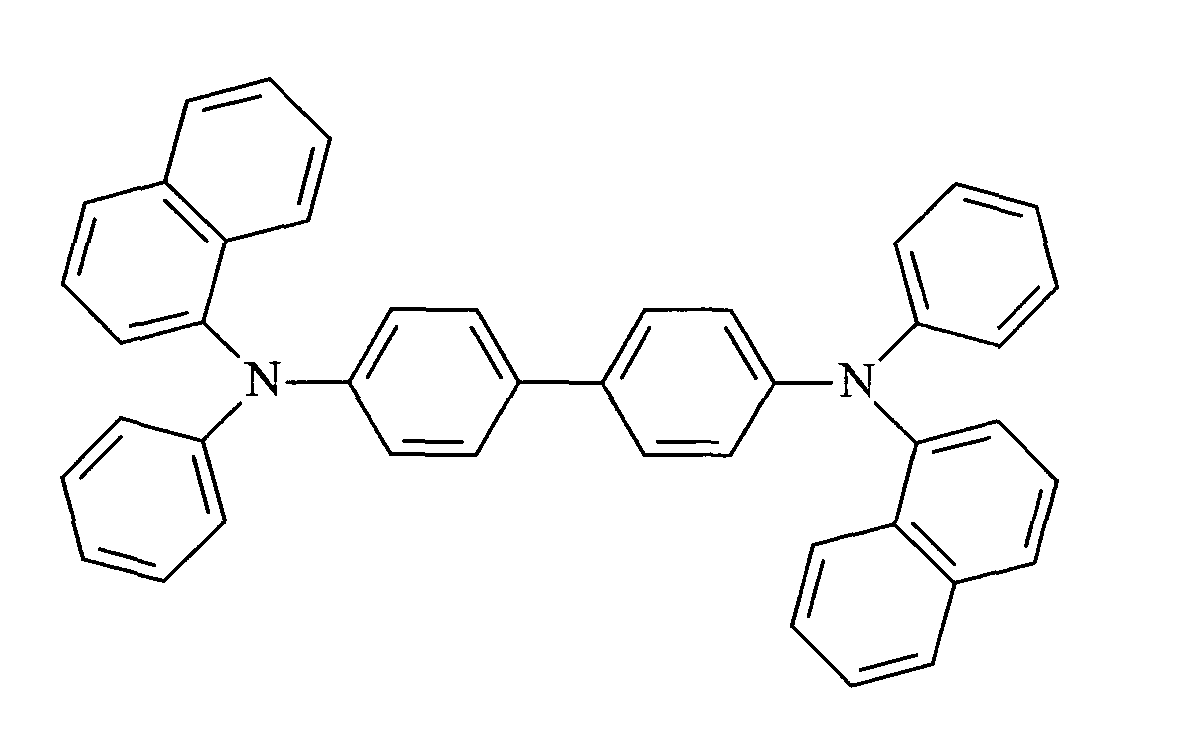
- a preferred class of tertiary aromatic amines that can be used in the luminescent region are the naphtyl-substituted benzidine derivatives, such as, N,N'-di(naphthalene-1-yl)-N,N'-diphenyl-benzidine (NPB).
- Another class of aromatic tertiary amines are polynuclear aromatic amines.
- polynuclear aromatic amines include, but are not limited to, N,N-bis-[4'-(N-phenyl-N-m-tolylamino)-4-biphenylyl]aniline; N,N-bis-[4'-(N-phenyl-N-m-tolylamino)-4-biphenylyl]-m-toluidine; N,N-bis-[4'-(N-phenyl-N-m-tolylamino)-4-biphenylyl]-p-toluidine; N,N-bis-[4'-(N-phenyl-N-p-tolylamino)-4-biphenylyl]aniline; N,N-bis-[4'-(N-phenyl-N-p-tolylamino)-4-biphenylyl]-m-toluidine; N,N-bis-[4'-(N-phenyl-N-p-tolylamino)
- a specific class of the hole transporting materials that can be used in the luminescent region are the indolo-carabazoles, such as those disclosed in U.S. Patents 5,942,340 and 5,952,115, such as 5,11-di-naphthyl-5,11-dihydroindolo[3,2-b]carbazole, and 2,8-dimethyl-5,11-di-naphthyl-5,11-dihydroindolo[3,2-b]carbazole; N,N,N'N'-tetraarylbenzidines, wherein aryl may be selected from phenyl, m-tolyl, p-tolyl, m-methoxyphenyl, p-methoxyphenyl, 1-naphthyl, 2-naphthyl and the like.
- N,N,N'N'-tetraarylbenzidine are N,N;-di-1-naphthyl -N,N'- diphenyl-1,1'-biphenyl-4,4'-diamine, which is more preferred; N,N'-bis(3-methylphenyl) -N,N'-diphenyl-1,1'-biphenyl-4,4'-diamine; N,N'-bis(3-methoxyphenyl) -N,N'- diphenyl-1,1'-biphenyl-4,4'-diamine, and the like.
- the luminescent region can include one or more non-anthracene and non-triazine derivative compounds which have the desired properties such as electron transporting and/or light emitting properties.
- a number of the following exemplary non-anthracene and non-triazine derivative compounds may have electron transporting and/or light emitting properties and thus may be useful in the luminescent region (in for example the light emitting zone and/or the electron transport zone): polyfluorenes, such as poly(9,9-di-n-octylfluorene-2,7-diyl), poly(2,8-(6,7,12,12-tetraalkylindenofluorene) and copolymers containing fluorenes such as fluorene-amine copolymers, as disclosed in incorporated Bernius et al., Proceedings of SPIE Conference on Organic Light Emitting Materials and Devices III, Denver, Colorado, July 1999, Volume 3797, p. 129.
- non-anthracene and non-triazine derivative compounds may include metal oxinoids as disclosed in U.S. Patents 4,539,507; 5,151,629; 5,150,006, 5,141,671, and 5,846,666.
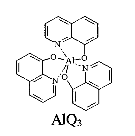
- Illustrative specific examples include tris(8-hydroxyquinolinate)aluminum(Alq 3 ), bis(8-hydroxyquinolato)-(4-phenylphenolato)aluminum (Balq).
- tris(8-hydroxyquinolinate) gallium bis(8-hydroxyquinolinate) magnesium, bis(8-hydroxyquinolinate) zinc, tris(5-methyl-8-hydroxyquinolinate) aluminum, tris(7-propyl-8-quinolinolato) aluminum, bis[benzo ⁇ f ⁇ -8-quinolinate]zinc, bis(10-hydroxybenzo[h] quinolinate) beryllium, and the like.
- non-anthracene and non-triazine derivative compounds are stilbene derivatives, such as those disclosed in U.S. Patent 5,516,577.
- Further examples of non-anthracene and non-triazine derivative compounds are the metal thioxinoid compounds, illustrated in U.S.
- Patent 5,846,666 the disclosure of which is totally incorporated herein by reference, such as metal thioxinoid compounds of bis(8-quinolinethiolato)zinc, bis(8-quinolinethiolato)cadmium, tris(8-quinolinethiolato)gallium, tris(8-quinolinethiolato)indium, bis(5-methylquinolinethiolato)zinc, tris(5-methylquinolinethiolato)gallium, tris(5-methylquinolinethiolato)indium, bis(5-methylquinolinethiolato)cadmium, bis(3-methylquinolinethiolato)cadmium, bis(5-methylquinolinethiolato)zinc, bis[benzo ⁇ f ⁇ -8-quinolinethiolato]zinc, bis[3-methylbenzo ⁇ f ⁇ -8-quinolinethiolato]zinc, bis[3,7-dimethylbenzo ⁇ f ⁇ -8-quinolinethiolato]zinc, and the like.
- non-anthracene and non-triazine derivative compounds are bis(8-quinolinethiolato)zinc, bis(8-quinolinethiolato) cadmium, tris(8-quinolinethiolato)gallium, tris(8-quinolinethiolato)indium and bis[benzo ⁇ f ⁇ -8-quinolinethiolato]zinc.
- Other suitable non-anthracene and non-triazine derivative compounds are the oxadiazole metal chelates disclosed in incorporated U.S.
- Patent 5,925,472 which materials include bis[2-(2-hydroxyphenyl)-5-phenyl-1,3,4-oxadiazolato]zinc; bis[2-(2-hydroxyphenyl)-5-phenyl-1,3,4-oxadiazolato]beryllium; bis[2-(2-hydroxyphenyl)-5-(1-naphthyl)-1,3,4-oxadiazolato]zinc; bis[2-(2-hydroxyphenyl)-5-(1-naphthyl)-1,3,4-oxadiazolato]beryllium; bis[5-biphenyl-2-(2-hydroxyphenyl)-1,3,4-oxadiazolato]zinc; bis[5-biphenyl-2-(2-hydroxyphenyl)-1,3,4-oxadiazolato]beryllium; bis(2-hydroxyphenyl)-5-phenyl-1,3,4-oxadiazolato]lithium; bis[2-(2-hydroxyphenyl
- non-anthracene and non-triazine derivative compounds are the quinolines, such as, for example, 1,4-bis(4-phenylquinolin-2-yl)benzene, 4,4'-bis(4-phenylquinolin-2-yl)-1,1'-biphenyl (TA).
- quinolines such as, for example, 1,4-bis(4-phenylquinolin-2-yl)benzene, 4,4'-bis(4-phenylquinolin-2-yl)-1,1'-biphenyl (TA).
- the organic electroluminescent material, the hole transport material(s), and/or the electron transport material(s) can be formed in separate layers, such as the OLEDs disclosed in U.S. Patents 4,539,507; 4,720,432 and 4,769,292; or in the same layer thus forming mixed areas of two or more materials, such as the OLEDs disclosed in U.S. Patents 5,853,905; 5,925,980; 6,130,001, 6,114,055; 6,392,250; 6,392,339.
- the thickness of the luminescent region can vary for example, from about 10 ⁇ to about 10,000 ⁇ , typically from about 200 ⁇ to about 2,000 ⁇ , and particularly from about 500 ⁇ to about 1,500 ⁇ .
- the thickness of each layer can, for example, be from about 10 ⁇ to about 5,000 ⁇ , typically from about 50 ⁇ to about 2,000 ⁇ , and particularly from about 100 ⁇ to about 1,500 ⁇ .
- Each layer of the OLED may have a generally uniform or non-uniform composition across the layer thickness where each layer is composed entirely of one material or a mixture of materials.
- the OLED can be fabricated by sequentially forming the desired layers on the substrate using any suitable thin film forming technique, typically, spin coating or deposition by thermal evaporation in vacuum. More details about fabrication and operation of organic light emitting devices are disclosed, for example, in U.S. Patents 4,539,507 and 4,769,292.
- Organic light emitting device can demonstrate an improved performance, such as, a higher operational stability and improved color purity, compared to other blue-emitting OLEDs, such as, for example, OLEDs containing an anthracene derivative compound as an emitting material and a quinoline-type metal chelate derivative compound (which is not a triazine derivative compound) as an electron transport material.
- OLEDs such as, for example, OLEDs containing an anthracene derivative compound as an emitting material and a quinoline-type metal chelate derivative compound (which is not a triazine derivative compound) as an electron transport material.
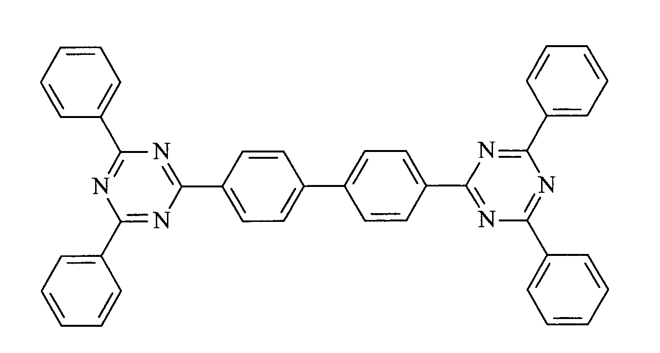
- An organic light emitting device (referred to herein as device A) of structure ITO anode (50 nm)/CuPc porphyrin compound buffer layer (15 nm)/NPB tertiary aromatic amine compound hole transport layer (30 nm) / BH2 anthracene derivative compound emitter layer (30 nm) / T1 triazine derivative compound electron transport layer (20 nm)/Mg:Ag cathode (9:1 volume ratio of Mg:Ag, 200 nm) was fabricated.
- the molecular structures of CuPc, NPB, BH2 and T1 are as follows:
- the device was fabricated by vacuum deposition at a base pressure of 5 ⁇ 10 -6 torr., where all organic layers, and the cathode were thermally evaporated, on ITO-coated glass substrates, pre-cleaned using UV-ozone cleaning.
- the driving voltage needed to operate the device at these conditions was 8.7 volts. After 60 hours of continuous operation at this current density in a nitrogen atmosphere, the decay in emission intensity was less than 1% of the initial intensity.
- An organic light emitting device (referred to herein as device B) of structure ITO anode (50 nm)/CuPc porphyrin compound buffer layer (15 nm)/NPB tertiary aromatic amine compound hole transport layer (30 nm) / BH2 anthracene derivative compound emitter layer (30 nm) / AlQ 3 quinoline-type metal chelate derivative compound electron transport layer (20 nm)/Mg:Ag cathode (9:1 volume ratio of Mg:Ag, 200 nm).
- the molecular structure of AlQ 3 is
- the device was fabricated by vacuum deposition at a base pressure of 5 ⁇ 10 -6 torr., where all organic layers, and the cathode were thermally evaporated, on ITO-coated glass substrates, pre-cleaned using UV-ozone cleaning.
- the driving voltage needed to operate the device at these conditions was 8.3 volts. After 60 hours of continuous operation at this current density in a nitrogen atmosphere, the decay in emission intensity was about 10% of the initial intensity.
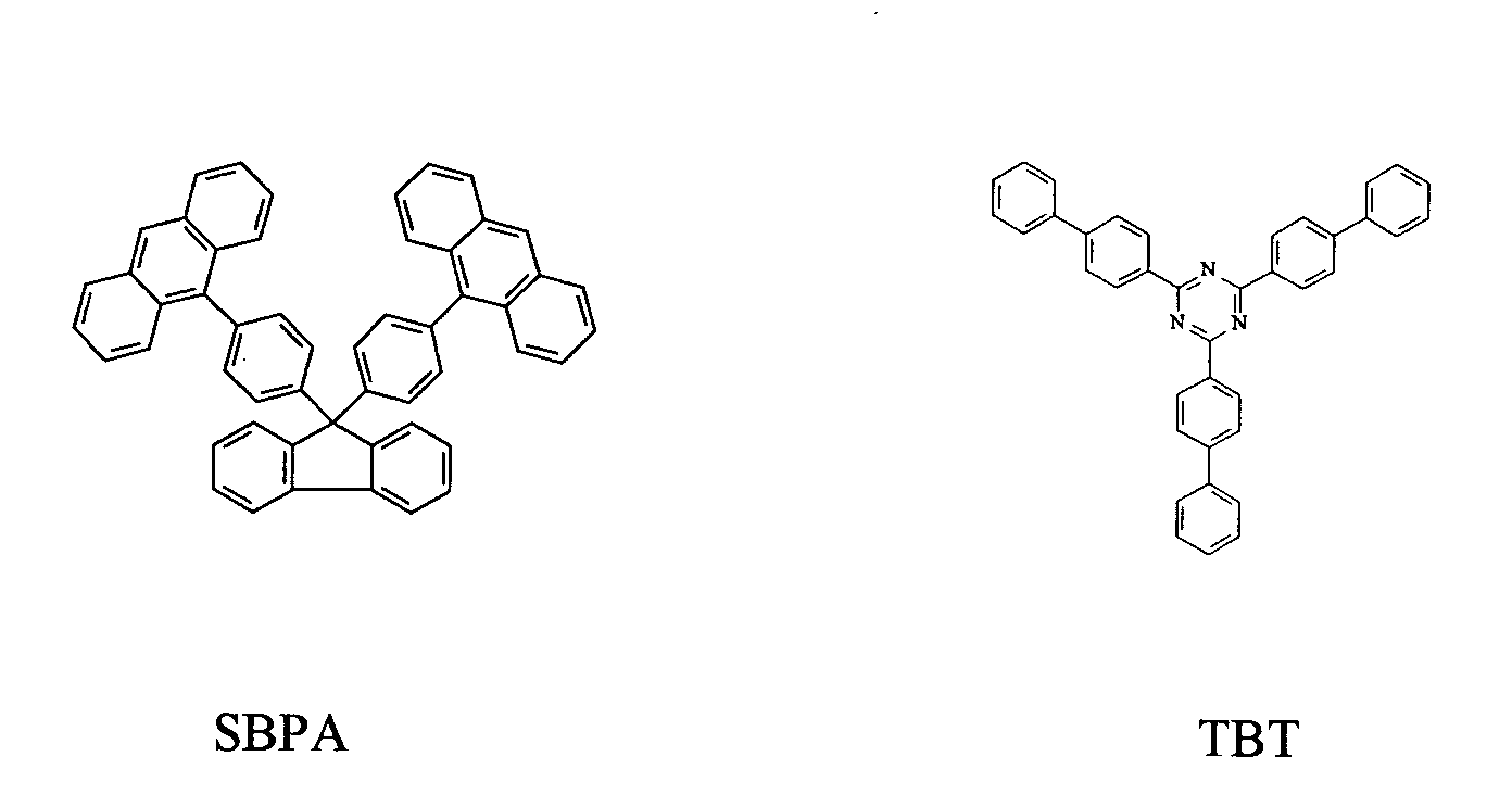
- An organic light emitting device (referred to herein as device C) of structure ITO anode (50 nm)/NPB tertiary aromatic amine compound hole transport layer (30 nm) / SBPA anthracene derivative compound emitter layer (42 nm) / TBT triazine derivative compound first electron transport layer (10 nm)/ AlQ 3 quinoline derivative compound second electron transport layer (20 nm) /Mg:Ag cathode (9:1 volume ratio of Mg:Ag, 200 nm) was fabricated.
- the molecular structures of SBPA and TBT are as follows:
- the device was fabricated by vacuum deposition at a base pressure of 5 ⁇ 10 -6 torr., where all organic layers, and the cathode were thermally evaporated, on ITO-coated glass substrates, pre-cleaned using UV-ozone cleaning.
- the driving voltage needed to operate the device at these conditions was 10.3 volts.
- An organic light emitting device (referred to herein as device D) of structure ITO anode (50 nm)/NPB tertiary aromatic amine compound hole transport layer (30 nm) / SBPA anthracene derivative compound emitter layer (42 nm) /AlQ 3 quinoline derivative compound electron transport layer (20 nm) /Mg:Ag cathode (9:1 volume ratio of Mg:Ag, 200 nm) was fabricated.
- the device was fabricated by vacuum deposition at a base pressure of 5 ⁇ 10 -6 torr., where all organic layers, and the cathode were thermally evaporated, on ITO-coated glass substrates, pre-cleaned using UV-ozone cleaning.
- the driving voltage needed to operate the device at these conditions was 9.3 volts.
- devices A and C illustrate that the improved performance of devices according to embodiments of this invention is not limited to a specific anthracene derivative compound or a specific triazine derivative compound. Rather utilizing a variety of anthracene derivative compounds and triazine derivative compounds can be used to produce organic light emitting devices with improved performance.
- An organic light emitting device (referred to herein as device E) of structure ITO anode (50 nm)/NPB tertiary aromatic amine compound hole transport layer (30 nm) / SBPA anthracene derivative compound doped with acridone blue luminescent material (1.6% by volume of the emitter layer) emitter layer (42 nm) / TBT triazine derivative compound first electron transport layer (10 nm)/ AlQ 3 quinoline derivative compound second electron transport layer (20 nm) /Mg:Ag cathode (9:1 volume ratio of Mg:Ag, 200 nm) was fabricated.
- the molecular structure of acridone blue luminescent material is
- the device was fabricated by vacuum deposition at a base pressure of 5 ⁇ 10 -6 torr., where all organic layers, and the cathode were thermally evaporated, on ITO-coated glass substrates, pre-cleaned using UV-ozone cleaning.
- the driving voltage needed to operate the device at these conditions was 10.4 volts.
- a group of organic light emitting devices (referred to herein as devices F-i through F-iii)) of structure ITO anode (50 nm)/CuPc porphyrin compound buffer layer (15 nm) / NPB tertiary aromatic amine compound hole transport layer (30 nm) / A first layer (2 nm) of the emitting zone composed of SBPA, and a second layer (35 nm) of the emitting zone composed of a mixture of SBPA anthracene derivative compound and TBT triazine derivative compound / TBT triazine derivative compound first electron transport layer (8 nm)/ T1 triazine derivative compound second electron transport layer (25 nm) /Mg:Ag cathode (9:1 volume ratio of Mg:Ag, 200 nm) was fabricated.
- the SBPA:TBT ratio in the second layer of the emitting zone was (100:0 by volume, i.e., no TBT); in device F-ii, the SBPA:TBT ratio in the second layer of the emitting zone was (95:5 by volume); and in device F-iii, the SBPA:TBT ratio in the second layer of the emitting zone was (75:25 by volume).
- the devices were fabricated by vacuum deposition at a base pressure of 5 ⁇ 10 -6 torr., where all organic layers, and the cathode were thermally evaporated, on ITO-coated glass substrates, pre-cleaned using UV-ozone cleaning.
- An organic light emitting devices (referred to herein as device G) of structure ITO anode (50 nm)/CuPc porphyrin compound buffer layer (15 nm) / NPB tertiary aromatic amine compound hole transport layer (50 nm) / A mixture of BH2 anthracene derivative compound and NPB tertiary aromatic amine charge transport compound (1:1 by volume) light emitting layer (25 nm) / A first layer (5 nm) of electron transport zone composed of BH2 anthracene derivative compound, and a second layer (20 nm) of electron transport zone composed of T1 triazine derivative compound / Mg:Ag cathode (9:1 volume ratio of Mg:Ag, 200 nm) was fabricated.
- the device was fabricated by vacuum deposition at a base pressure of 5 ⁇ 10 -6 torr., where all organic layers, and the cathode were thermally evaporated, on ITO-coated glass substrates, pre-cleaned using UV-ozone cleaning.
- the driving voltage needed to operate the device at these conditions was 8.1 volts. After 600 hours of continuous operation at this current density in a nitrogen atmosphere, the decay in emission intensity was only about 10% of the initial intensity.
- blue-emitting OLEDs are more suitable for potential technological applications, as they are able to provide better performance compared to other blue-emitting OLEDs.
Landscapes
- Chemical & Material Sciences (AREA)
- Organic Chemistry (AREA)
- Physics & Mathematics (AREA)
- Engineering & Computer Science (AREA)
- Materials Engineering (AREA)
- Spectroscopy & Molecular Physics (AREA)
- Optics & Photonics (AREA)
- Electroluminescent Light Sources (AREA)
- Nitrogen Condensed Heterocyclic Rings (AREA)
Abstract
Description










Claims (8)
- A device comprising:an anode;a cathode; anda luminescent region between the cathode and the anode, wherein the luminescent region comprises an anthracene derivative compound and a triazine derivative compound.
- The device according to claim 1 wherein the luminescent region includes at least a light emitting zone and an electron transport zone.
- The device of claim 2 which further includes a hole transport zone.
- The device according to claim 1 wherein the anthracene derivative compound is selected from the group consisting of formulas I(A)(1) through I(A)(11), formula I(B), formula I(C), and formula I(D):


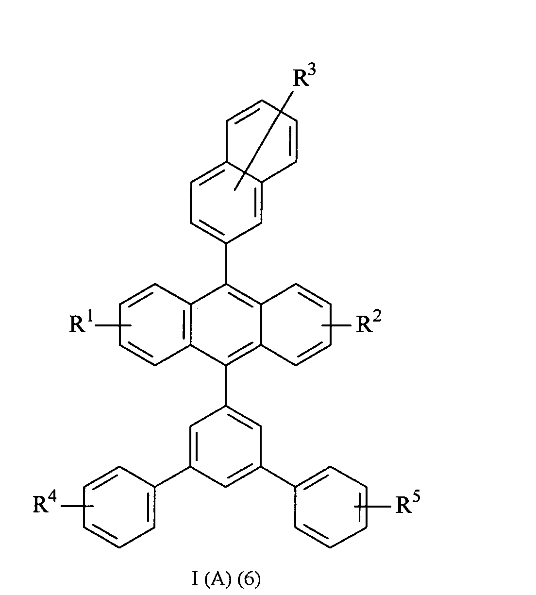
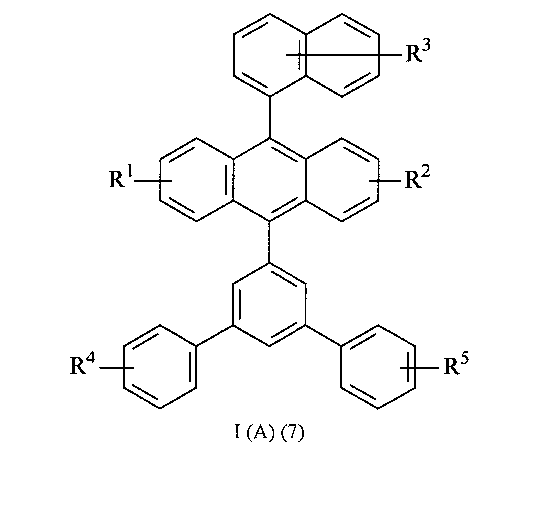


 wherein substituents R1, R2, R3, R4, R5 and R6 are each independently selected from the group consisting of: hydrogen; alkyl of from 1 to 24 carbon atoms; alkoxy of from 1 to 9 carbon atoms; triphenylsilyl; aryl of from 6 to 20 carbon atoms that is optionally substituted; heteroaryl of from 5 to 24 carbon atoms that is optionally substituted; halogen; and cyano group;
 wherein substituents R7, R8, R9, and R10 are each independently selected from the group consisting of:
 wherein substituents R11, R12, R13, and R14 are each independently selected from the group consisting of:Group 1: hydrogen, or alkyl of from 1 to 24 carbon atoms;Group 2: aryl from 6 to 20 carbon atoms that is optionally substituted;Group 3: carbon atoms necessary to complete a fused aromatic ring of naphthyl, anthracenyl, pyrenyl, or perylenyl;Group 4: heteroaryl of from 5 to 24 carbon atoms that is optionally substituted;Group 5: a fused heteroaromatic ring of furyl, thienyl, pyridyl, or quinolinyl;Group 6: alkoxy, amino, alkyl amino, or aryl amino group of from 1 to 24 carbon atoms; andGroup 7: fluorine, chlorine, bromine or cyano;
 wherein R15 and R16 are independently selected from the group consisting of hydrogen, an alkyl group with from 1 to about 6 carbon atoms, an aryl group with about 6 to about 30 carbon atoms;Group 1: hydrogen, or alkyl of from 1 to 24 carbon atoms;Group 2: aryl of from 6 to 20 carbon atoms that is optionally substituted;Group 3: carbon atoms necessary to complete a fused aromatic ring of naphthyl, anthracenyl, pyrenyl, or perylenyl;Group 4: heteroaryl of from 5 to 24 carbon atoms that is optionally substituted, carbon atoms necessary to complete a fused heteroaromatic ring of furyl, thienyl, pyridyl, quinolinyl;Group 5: alkoxy, amino, alkyl amino, or aryl amino group of from 1 to 24 carbon atoms; andGroup 6: fluorine, chlorine, bromine or cyano;
X and Y are independently selected from the group consisting of hydrogen, an alkyl group with from 1 to about 6 carbon atoms, an aryl group with about 6 to about 30 carbon atoms, an alkoxy group with from 1 to about 6 carbon atoms, a halogen, a cyano group; and
the triazine derivative compound is selected from the group consisting of formulas II(A), II(B), II(C), and II(D):
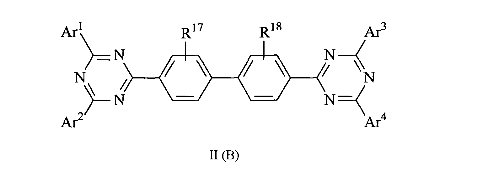
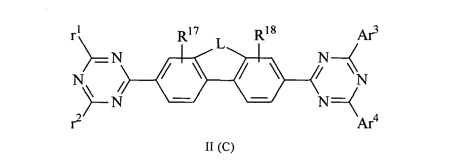 wherein Ar1, Ar2, Ar3, and Ar4 are each independently aryl of from 6 to about 20 carbon atoms that is optionally substituted;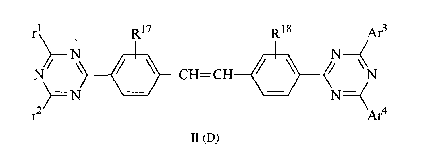
R17 to R18 are independently selected from the group consisting of hydrogen, an aliphatic with from 1 to about 6 carbon atoms, an alkoxy group with from 1 to about 6 carbon atoms, a halogen, a cyano group; and
L is a divalent group selected from the group consisting of ―C(R'R")―, an ethylene, ―Si(R'R")―, an oxygen atom, a sulfur atom, wherein R' and R" are each independently a hydrogen atom, an alkyl group containing from 1 to about 10 carbon atoms, and an alkoxyl group containing from 1 to about 10 carbon atoms. - The device of claim 4, wherein the anthracene derivative compound is selected from the group consisting of the formula I(A)(4) and the formula I(D).
- The device of claim 4, wherein the triazine derivative compound is selected from the formula II(B).
- The device of claim 4, wherein the anthracene derivative compound isBH2.
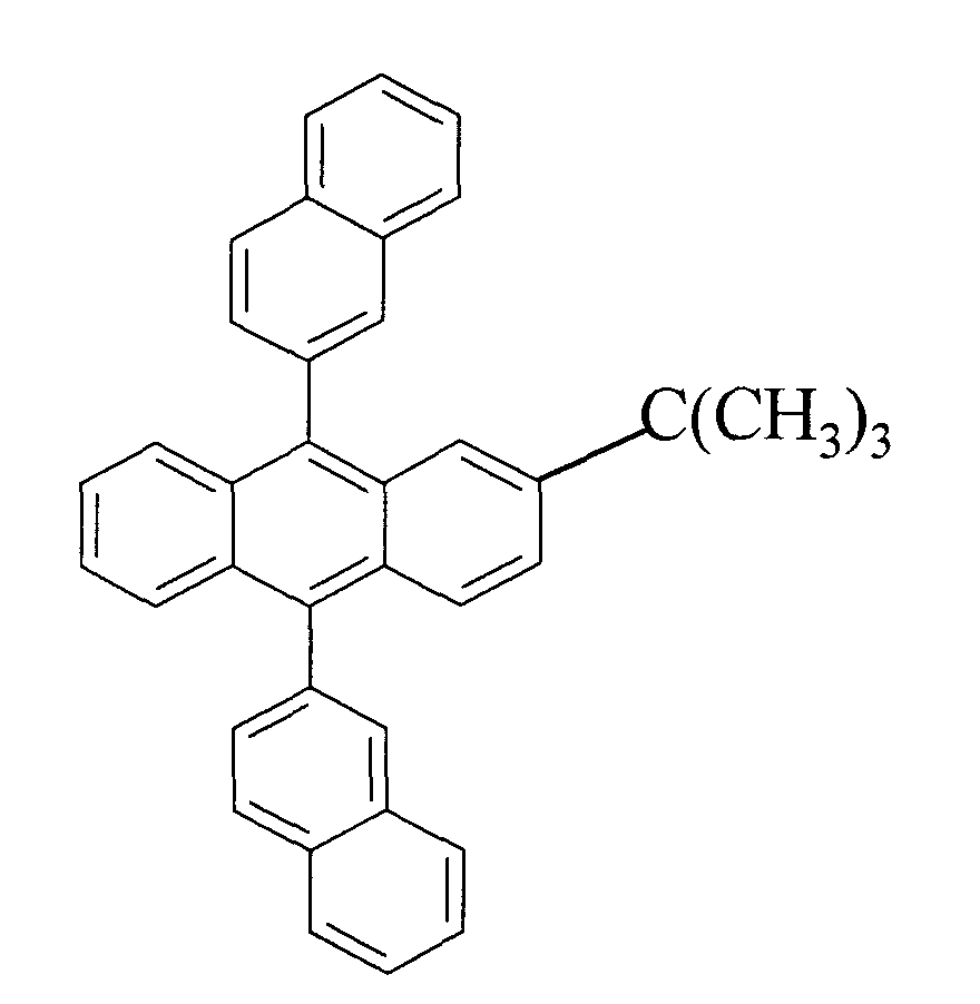
- The device of claim 1, wherein the anthracene derivative compound isBH2.

Applications Claiming Priority (4)
| Application Number | Priority Date | Filing Date | Title |
|---|---|---|---|
| US10/207,686 US20040018380A1 (en) | 2002-07-26 | 2002-07-26 | Display device with anthracene and triazine derivatives |
| US207686 | 2002-07-26 | ||
| US10/372,547 US7169482B2 (en) | 2002-07-26 | 2003-02-24 | Display device with anthracene and triazine derivatives |
| US372547 | 2003-02-24 |
Publications (3)
| Publication Number | Publication Date |
|---|---|
| EP1385221A2 true EP1385221A2 (en) | 2004-01-28 |
| EP1385221A3 EP1385221A3 (en) | 2006-03-22 |
| EP1385221B1 EP1385221B1 (en) | 2015-12-02 |
Family
ID=30002717
Family Applications (1)
| Application Number | Title | Priority Date | Filing Date |
|---|---|---|---|
| EP03254473.6A Expired - Lifetime EP1385221B1 (en) | 2002-07-26 | 2003-07-17 | Display device with anthracene and triazine derivtives |
Country Status (4)
| Country | Link |
|---|---|
| US (1) | US7169482B2 (en) |
| EP (1) | EP1385221B1 (en) |
| JP (1) | JP4772280B2 (en) |
| CN (1) | CN1482691B (en) |
Cited By (11)
| Publication number | Priority date | Publication date | Assignee | Title |
|---|---|---|---|---|
| WO2005042668A1 (en) * | 2003-10-24 | 2005-05-12 | Eastman Kodak Company | Electroluminescent device with anthracene derivative host |
| WO2005053055A1 (en) * | 2003-11-27 | 2005-06-09 | Merck Patent Gmbh | Organic electroluminescent element |
| WO2005080527A1 (en) * | 2004-02-17 | 2005-09-01 | Eastman Kodak Company | Anthracene derivative host having ranges of dopants |
| EP1640430A1 (en) | 2004-07-09 | 2006-03-29 | Chisso Corporation | Luminescent material and organic electroluminescent device using the same |
| EP1669428A1 (en) * | 2004-12-07 | 2006-06-14 | L.G. Philips LCD Co., Ltd. | Organic electroluminescent devices |
| US7887931B2 (en) | 2003-10-24 | 2011-02-15 | Global Oled Technology Llc | Electroluminescent device with anthracene derivative host |
| US8076676B2 (en) | 2006-06-01 | 2011-12-13 | Semiconductor Energy Laboratory Co., Ltd. | Light-emitting element, light-emitting device and an electronic device which include two layers including the same light-emitting organic compound |
| WO2014168386A1 (en) * | 2013-04-08 | 2014-10-16 | 주식회사 엘엠에스 | Novel compound, and light-emitting device and electronic device including same |
| EP2145937B2 (en) † | 2002-08-23 | 2016-03-02 | Idemitsu Kosan Co., Ltd. | Organic electroluminescence device and anthracene derivative |
| US9397308B2 (en) | 2006-12-04 | 2016-07-19 | Semiconductor Energy Laboratory Co., Ltd. | Light emitting element, light emitting device, and electronic device |
| US9680110B2 (en) | 2006-08-31 | 2017-06-13 | Cdt Oxford Limited | Compounds for use in opto-electrical devices |
Families Citing this family (124)
| Publication number | Priority date | Publication date | Assignee | Title |
|---|---|---|---|---|
| US6832570B2 (en) | 2002-07-26 | 2004-12-21 | Karl L. Aschenbach | Fender with compact spring element |
| US7400261B2 (en) * | 2003-04-11 | 2008-07-15 | Semiconductor Energy Laboratory Co., Ltd. | Display device, and vehicle-mounted display device and electronic |
| TW200515836A (en) * | 2003-10-22 | 2005-05-01 | Hannstar Display Corp | Organic electroluminescent element |
| KR101031412B1 (en) | 2003-12-19 | 2011-04-26 | 이데미쓰 고산 가부시키가이샤 | Luminescent materials for organic electroluminescent devices, organic electroluminescent devices and materials for organic electroluminescent devices using the same |
| US7030554B2 (en) * | 2004-02-06 | 2006-04-18 | Eastman Kodak Company | Full-color organic display having improved blue emission |
| DE102004010145A1 (en) * | 2004-02-27 | 2005-09-15 | H.C. Starck Gmbh | Deformable electroluminescent device |
| US20060036114A1 (en) * | 2004-08-13 | 2006-02-16 | Suning Wang | Organoboron luminescent compounds and methods of making and using same |
| JP4536730B2 (en) * | 2004-09-02 | 2010-09-01 | エルジー・ケム・リミテッド | Anthracene derivative and organic light emitting device using the same as luminescent material |
| GB0424294D0 (en) * | 2004-11-03 | 2004-12-01 | Elam T Ltd | Buffer layer |
| WO2006059734A1 (en) * | 2004-11-30 | 2006-06-08 | Semiconductor Energy Laboratory Co., Ltd. | Light emitting element and light emitting device having the light emitting element |
| US7351999B2 (en) * | 2004-12-16 | 2008-04-01 | Au Optronics Corporation | Organic light-emitting device with improved layer structure |
| US20060159952A1 (en) * | 2005-01-14 | 2006-07-20 | Eastman Kodak Company | Mixed anthracene derivative host materials |
| JP4907090B2 (en) * | 2005-02-17 | 2012-03-28 | 東ソー株式会社 | 1,3,5-triazine derivative |
| JP2006225321A (en) * | 2005-02-17 | 2006-08-31 | Tosoh Corp | Thin film comprising 1,3,5-triazine derivative and method for producing the same |
| KR100787428B1 (en) * | 2005-03-05 | 2007-12-26 | 삼성에스디아이 주식회사 | Organic electroluminescent element |
| CN101853923B (en) * | 2005-04-21 | 2013-05-22 | 株式会社半导体能源研究所 | Light emitting element, light emitting device, and electronic device |
| US7777407B2 (en) * | 2005-05-04 | 2010-08-17 | Lg Display Co., Ltd. | Organic light emitting devices comprising a doped triazine electron transport layer |
| US8487527B2 (en) * | 2005-05-04 | 2013-07-16 | Lg Display Co., Ltd. | Organic light emitting devices |
| US7811679B2 (en) * | 2005-05-20 | 2010-10-12 | Lg Display Co., Ltd. | Display devices with light absorbing metal nanoparticle layers |
| US7728517B2 (en) * | 2005-05-20 | 2010-06-01 | Lg Display Co., Ltd. | Intermediate electrodes for stacked OLEDs |
| US7795806B2 (en) | 2005-05-20 | 2010-09-14 | Lg Display Co., Ltd. | Reduced reflectance display devices containing a thin-layer metal-organic mixed layer (MOML) |
| US7750561B2 (en) * | 2005-05-20 | 2010-07-06 | Lg Display Co., Ltd. | Stacked OLED structure |
| US7943244B2 (en) * | 2005-05-20 | 2011-05-17 | Lg Display Co., Ltd. | Display device with metal-organic mixed layer anodes |
| US20060269782A1 (en) * | 2005-05-25 | 2006-11-30 | Eastman Kodak Company | OLED electron-transporting layer |
| WO2007016454A2 (en) * | 2005-07-29 | 2007-02-08 | University Of Rochester | Light-emitting organic materials |
| EP1930329B1 (en) * | 2005-08-26 | 2012-10-24 | Tosoh Corporation | 1,3,5-triazine derivative, method for producing same, and organic electroluminescent device containing same as component |
| TWI257946B (en) * | 2005-08-31 | 2006-07-11 | Chunghwa Picture Tubes Ltd | Organic electro-luminescence device and material of hole transport layer |
| US9666826B2 (en) * | 2005-11-30 | 2017-05-30 | Global Oled Technology Llc | Electroluminescent device including an anthracene derivative |
| US7553558B2 (en) | 2005-11-30 | 2009-06-30 | Eastman Kodak Company | Electroluminescent device containing an anthracene derivative |
| US20070141388A1 (en) * | 2005-12-16 | 2007-06-21 | Eastman Kodak Company | Electroluminescent device containing a butadiene derivative |
| US7858207B2 (en) * | 2005-12-21 | 2010-12-28 | Lg Display Co., Ltd. | Host material for organic electroluminescence devices |
| CN100361980C (en) * | 2005-12-29 | 2008-01-16 | 中国科学院上海有机化学研究所 | A New Blue Light Material--Anthracene Derivatives Containing Triazine Ring |
| US20070252515A1 (en) * | 2006-04-27 | 2007-11-01 | Eastman Kodak Company | Electroluminescent device including an anthracene derivative |
| US7733009B2 (en) * | 2006-04-27 | 2010-06-08 | Global Oled Technology Llc | Electroluminescent device including an anthracene derivative |
| KR100903203B1 (en) * | 2006-11-30 | 2009-06-18 | 에스에프씨 주식회사 | Anthracene Derivatives and Organic Electroluminescent Devices Employing the Same |
| JP5326289B2 (en) * | 2007-03-23 | 2013-10-30 | 凸版印刷株式会社 | ORGANIC EL ELEMENT AND DISPLAY DEVICE INCLUDING THE SAME |
| JP5580733B2 (en) * | 2007-05-09 | 2014-08-27 | 東進セミケム株式会社 | Novel anthracene compound and organic light emitting device using the same |
| KR101442240B1 (en) | 2007-10-01 | 2014-10-01 | 동우 화인켐 주식회사 | Organosilane Compounds, Materials Comprising The Same For Organic Electroluminescent Device, and Organic Electroluminescent Device |
| US8076009B2 (en) * | 2007-10-26 | 2011-12-13 | Global Oled Technology, Llc. | OLED device with fluoranthene electron transport materials |
| US20090267891A1 (en) * | 2008-04-25 | 2009-10-29 | Bamidele Ali | Virtual paper |
| CN103258964B (en) | 2008-05-16 | 2016-06-01 | 株式会社半导体能源研究所 | Luminous element, electronics and means of illumination |
| JP5748948B2 (en) | 2008-10-03 | 2015-07-15 | 東ソー株式会社 | 1,3,5-triazine derivative, method for producing the same, and organic electroluminescent device comprising the same |
| TWI475011B (en) | 2008-12-01 | 2015-03-01 | 東曹股份有限公司 | 1,3,5-triazabenzene derivative, a process for producing the same, and an organic electroluminescence device comprising the same |
| JP5371404B2 (en) * | 2008-12-10 | 2013-12-18 | 凸版印刷株式会社 | Electron transporting material and light emitting device |
| EP2462203B1 (en) | 2009-08-04 | 2016-03-02 | Merck Patent GmbH | Electronic devices comprising multi cyclic hydrocarbons |
| WO2011076326A1 (en) | 2009-12-22 | 2011-06-30 | Merck Patent Gmbh | Electroluminescent functional surfactants |
| JP5968786B2 (en) | 2009-12-22 | 2016-08-10 | メルク パテント ゲーエムベーハー | Electroluminescence formulation |
| WO2011076323A1 (en) | 2009-12-22 | 2011-06-30 | Merck Patent Gmbh | Formulations comprising phase-separated functional materials |
| DE102010009193B4 (en) | 2010-02-24 | 2022-05-19 | MERCK Patent Gesellschaft mit beschränkter Haftung | Composition containing fluorine-fluorine associates, processes for their production, their use and organic electronic devices containing them |
| KR101757016B1 (en) | 2010-03-11 | 2017-07-11 | 메르크 파텐트 게엠베하 | Radiative fibers |
| WO2011110277A1 (en) | 2010-03-11 | 2011-09-15 | Merck Patent Gmbh | Fibers in therapy and cosmetics |
| JP5944380B2 (en) | 2010-05-27 | 2016-07-05 | メルク パテント ゲーエムベーハー | Composition comprising quantum dots |
| CN106887522B (en) | 2010-07-26 | 2018-09-18 | 默克专利有限公司 | Include the device of nanocrystal |
| EP2599141B1 (en) | 2010-07-26 | 2019-12-11 | Merck Patent GmbH | Quantum dots and hosts |
| WO2012110178A1 (en) | 2011-02-14 | 2012-08-23 | Merck Patent Gmbh | Device and method for treatment of cells and cell tissue |
| WO2012126566A1 (en) | 2011-03-24 | 2012-09-27 | Merck Patent Gmbh | Organic ionic functional materials |
| JP6223961B2 (en) | 2011-05-12 | 2017-11-01 | メルク パテント ゲーエムベーハー | Organic ionic functional material, composition and electronic device |
| US8247142B1 (en) * | 2011-06-30 | 2012-08-21 | Xerox Corporation | Fluorinated structured organic film compositions |
| US9385337B2 (en) | 2012-01-30 | 2016-07-05 | Merck Patent Gmbh | Nanocrystals on fibers |
| CN102916035B (en) * | 2012-08-28 | 2015-04-22 | 江苏三月光电科技有限公司 | Large-size full-color OLED (Organic Light-Emitting Diode) display |
| KR102104637B1 (en) * | 2013-06-28 | 2020-04-27 | 삼성디스플레이 주식회사 | Organic Light Emitting Diode Device |
| US10289271B2 (en) * | 2013-07-09 | 2019-05-14 | Sony Corporation | Information processing device and information processing method for displaying menu with orthogonal sub-menus |
| KR102084170B1 (en) * | 2013-07-25 | 2020-03-04 | 삼성디스플레이 주식회사 | An organic light emitting device, an organic light emitting display appratus having the organic light emitting device and a method of manufacturing the same |
| US10615343B2 (en) | 2014-09-05 | 2020-04-07 | Merck Patent Gmbh | Formulations and electronic devices |
| KR101848347B1 (en) * | 2014-10-28 | 2018-05-24 | 삼성에스디아이 주식회사 | Organic optoelectric device and display device |
| KR102330221B1 (en) | 2014-11-05 | 2021-11-25 | 삼성디스플레이 주식회사 | Organic light emitting device and display having the same |
| WO2016107663A1 (en) | 2014-12-30 | 2016-07-07 | Merck Patent Gmbh | Formulations and electronic devices |
| EP3278377B1 (en) | 2015-03-30 | 2020-08-05 | Merck Patent GmbH | Formulation of an organic functional material comprising a siloxane solvent |
| CN107690720B (en) | 2015-06-12 | 2020-04-03 | 默克专利有限公司 | Esters containing non-aromatic rings as solvents for OLED formulations |
| WO2017036572A1 (en) | 2015-08-28 | 2017-03-09 | Merck Patent Gmbh | Formulation of an organic functional material comprising an epoxy group containing solvent |
| KR102427671B1 (en) * | 2015-09-07 | 2022-08-02 | 삼성디스플레이 주식회사 | Organic light emitting device |
| KR102721890B1 (en) | 2015-12-10 | 2024-10-24 | 메르크 파텐트 게엠베하 | Formulations comprising a ketone containing a non-aromatic cycle |
| JP7051684B2 (en) | 2015-12-15 | 2022-04-11 | メルク パテント ゲーエムベーハー | Esters containing aromatic groups as solvents for organic electronic formulations |
| JP7438661B2 (en) | 2015-12-16 | 2024-02-27 | メルク パテント ゲーエムベーハー | Formulations containing solid solvents |
| KR20180095028A (en) | 2015-12-16 | 2018-08-24 | 메르크 파텐트 게엠베하 | A formulation containing a mixture of two or more different solvents |
| KR102776731B1 (en) | 2016-02-17 | 2025-03-05 | 메르크 파텐트 게엠베하 | Formulation of organic functional materials |
| DE102016003104A1 (en) | 2016-03-15 | 2017-09-21 | Merck Patent Gmbh | Container comprising a formulation containing at least one organic semiconductor |
| KR102543575B1 (en) | 2016-04-07 | 2023-06-14 | 삼성디스플레이 주식회사 | Organic light emitting diode |
| KR102467109B1 (en) | 2016-05-11 | 2022-11-14 | 메르크 파텐트 게엠베하 | Composition for electrochemical cells |
| JP2019523997A (en) | 2016-06-16 | 2019-08-29 | メルク パテント ゲーエムベーハー | Formulation of organic functional materials |
| WO2017216128A1 (en) | 2016-06-17 | 2017-12-21 | Merck Patent Gmbh | Formulation of an organic functional material |
| TW201815998A (en) | 2016-06-28 | 2018-05-01 | 德商麥克專利有限公司 | Organic functional material formulation |
| WO2018024719A1 (en) | 2016-08-04 | 2018-02-08 | Merck Patent Gmbh | Formulation of an organic functional material |
| US10461259B2 (en) | 2016-10-18 | 2019-10-29 | Lg Chem, Ltd. | Organic light emitting device |
| KR102451842B1 (en) | 2016-10-31 | 2022-10-07 | 메르크 파텐트 게엠베하 | Formulation of organic functional materials |
| EP3532566B1 (en) | 2016-10-31 | 2021-04-21 | Merck Patent GmbH | Formulation of an organic functional material |
| TWI756292B (en) | 2016-11-14 | 2022-03-01 | 德商麥克專利有限公司 | Compounds having an acceptor group and a donor group |
| US10892414B2 (en) | 2016-12-06 | 2021-01-12 | Merck Patent Gmbh | Process for making electronic device |
| KR102486614B1 (en) | 2016-12-13 | 2023-01-09 | 메르크 파텐트 게엠베하 | Formulation of organic functional materials |
| EP3560003A1 (en) | 2016-12-22 | 2019-10-30 | Merck Patent GmbH | Mixtures comprising at least two organofunctional compounds |
| TWI791481B (en) | 2017-01-30 | 2023-02-11 | 德商麥克專利有限公司 | Method for forming an organic electroluminescence (el) element |
| TWI763772B (en) | 2017-01-30 | 2022-05-11 | 德商麥克專利有限公司 | Method for forming an organic element of an electronic device |
| WO2018178136A1 (en) | 2017-03-31 | 2018-10-04 | Merck Patent Gmbh | Printing method for an organic light emitting diode (oled) |
| WO2018189050A1 (en) | 2017-04-10 | 2018-10-18 | Merck Patent Gmbh | Formulation of an organic functional material |
| KR20250036969A (en) | 2017-04-26 | 2025-03-14 | 오티아이 루미오닉스 인크. | Method for patterning a coating on a surface and device including a patterned coating |
| JP7330898B2 (en) | 2017-05-03 | 2023-08-22 | メルク パテント ゲーエムベーハー | Formulation of organic functional material |
| CN110892543B (en) | 2017-07-18 | 2023-07-28 | 默克专利有限公司 | Preparation of organic functional material |
| JP7293229B2 (en) | 2017-12-15 | 2023-06-19 | メルク パテント ゲーエムベーハー | Formulation of organic functional material |
| US11751415B2 (en) | 2018-02-02 | 2023-09-05 | Oti Lumionics Inc. | Materials for forming a nucleation-inhibiting coating and devices incorporating same |
| KR102710151B1 (en) | 2018-02-26 | 2024-09-25 | 메르크 파텐트 게엠베하 | Formulation of organic functional materials |
| WO2019238782A1 (en) | 2018-06-15 | 2019-12-19 | Merck Patent Gmbh | Formulation of an organic functional material |
| JP7325731B2 (en) | 2018-08-23 | 2023-08-15 | 国立大学法人九州大学 | organic electroluminescence element |
| EP3857621B1 (en) | 2018-09-24 | 2025-10-29 | Merck Patent GmbH | Method for the production of a granular material |
| JP7129392B2 (en) * | 2018-10-26 | 2022-09-01 | キヤノン株式会社 | COMPOSITION, ORGANIC LIGHT-EMITTING DEVICE, DISPLAY DEVICE, IMAGING DEVICE, ELECTRONIC DEVICE AND MOBILE BODY HAVING THE SAME |
| JP2022506510A (en) | 2018-11-06 | 2022-01-17 | メルク パテント ゲーエムベーハー | How to Form Organic Devices for Electronic Devices |
| CN116456753A (en) | 2019-03-07 | 2023-07-18 | Oti照明公司 | Optoelectronic device |
| KR20250110358A (en) | 2019-04-18 | 2025-07-18 | 오티아이 루미오닉스 인크. | Materials for forming a nucleation-inhibiting coating and devices incorporating the same |
| WO2020225778A1 (en) | 2019-05-08 | 2020-11-12 | Oti Lumionics Inc. | Materials for forming a nucleation-inhibiting coating and devices incorporating same |
| KR102148296B1 (en) * | 2019-07-29 | 2020-08-26 | 에스에프씨주식회사 | Organic light emitting diode including boron compounds |
| JP2023015412A (en) * | 2019-11-08 | 2023-02-01 | 出光興産株式会社 | Organic electroluminescence device and electronic device |
| EP4139971A1 (en) | 2020-04-21 | 2023-03-01 | Merck Patent GmbH | Emulsions comprising organic functional materials |
| JP2023522243A (en) | 2020-04-21 | 2023-05-29 | メルク パテント ゲーエムベーハー | Formulation of organic functional material |
| CN115867426A (en) | 2020-06-23 | 2023-03-28 | 默克专利有限公司 | method of producing the mixture |
| US12672476B2 (en) | 2020-10-29 | 2026-06-30 | Oti Lumionics Inc. | Opto-electronic device with nanoparticle deposited layers |
| KR20250139404A (en) | 2020-12-07 | 2025-09-23 | 오티아이 루미오닉스 인크. | Patterning a conductive deposited layer using a nucleation inhibiting coating and an underlying metallic coating |
| KR20230114756A (en) | 2020-12-08 | 2023-08-01 | 메르크 파텐트 게엠베하 | Ink Systems and Methods for Inkjet Printing |
| US20240244957A1 (en) | 2021-04-23 | 2024-07-18 | Merck Patent KGaA | Formulation of an organic functional material |
| WO2022243403A1 (en) | 2021-05-21 | 2022-11-24 | Merck Patent Gmbh | Method for the continuous purification of at least one functional material and device for the continuous purification of at least one functional material |
| WO2026008710A1 (en) | 2024-07-05 | 2026-01-08 | Merck Patent Gmbh | Cyclic silicon compounds for organic electroluminescent devices |
| WO2026041632A1 (en) | 2024-08-21 | 2026-02-26 | Merck Patent Gmbh | Heterocyclic materials for organic light-emitting devices |
| WO2026073855A1 (en) | 2024-10-01 | 2026-04-09 | Merck Patent Gmbh | Silicon compounds for organic electroluminescent devices |
| WO2026104430A1 (en) | 2024-11-14 | 2026-05-21 | Merck Patent Gmbh | Use of silicon compounds in an electronic device |
| WO2026131611A1 (en) | 2024-12-17 | 2026-06-25 | Merck Patent Gmbh | Silicon compounds for organic electroluminescent devices |
| WO2026153982A1 (en) | 2025-01-17 | 2026-07-23 | Merck Patent Gmbh | Materials for organic electroluminescent devices |
Family Cites Families (13)
| Publication number | Priority date | Publication date | Assignee | Title |
|---|---|---|---|---|
| JPH07157473A (en) * | 1993-12-06 | 1995-06-20 | Chisso Corp | Triazine derivative, its production and electric field luminescent element using the same |
| JP3284766B2 (en) * | 1994-06-29 | 2002-05-20 | 三菱化学株式会社 | Organic electroluminescent device |
| JP4514841B2 (en) * | 1998-02-17 | 2010-07-28 | 淳二 城戸 | Organic electroluminescent device |
| US5972247A (en) * | 1998-03-20 | 1999-10-26 | Eastman Kodak Company | Organic electroluminescent elements for stable blue electroluminescent devices |
| US5935721A (en) * | 1998-03-20 | 1999-08-10 | Eastman Kodak Company | Organic electroluminescent elements for stable electroluminescent |
| US6057048A (en) * | 1998-10-01 | 2000-05-02 | Xerox Corporation | Electroluminescent (EL) devices |
| US6229012B1 (en) * | 1998-10-01 | 2001-05-08 | Xerox Corporation | Triazine compositions |
| US6465115B2 (en) * | 1998-12-09 | 2002-10-15 | Eastman Kodak Company | Electroluminescent device with anthracene derivatives hole transport layer |
| US6361886B2 (en) * | 1998-12-09 | 2002-03-26 | Eastman Kodak Company | Electroluminescent device with improved hole transport layer |
| US6225467B1 (en) * | 2000-01-21 | 2001-05-01 | Xerox Corporation | Electroluminescent (EL) devices |
| JP4788078B2 (en) * | 2000-09-20 | 2011-10-05 | コニカミノルタホールディングス株式会社 | ORGANIC ELECTROLUMINESCENT ELEMENT, ORGANIC ELECTROLUMINESCENT ELEMENT MATERIAL, AND DISPLAY DEVICE |
| JP4404473B2 (en) * | 2000-12-25 | 2010-01-27 | 富士フイルム株式会社 | Novel nitrogen-containing heterocyclic compounds, light emitting device materials, and light emitting devices using them |
| US6720090B2 (en) * | 2001-01-02 | 2004-04-13 | Eastman Kodak Company | Organic light emitting diode devices with improved luminance efficiency |
-
2003
- 2003-02-24 US US10/372,547 patent/US7169482B2/en not_active Expired - Lifetime
- 2003-07-17 EP EP03254473.6A patent/EP1385221B1/en not_active Expired - Lifetime
- 2003-07-22 JP JP2003199678A patent/JP4772280B2/en not_active Expired - Lifetime
- 2003-07-25 CN CN031328881A patent/CN1482691B/en not_active Expired - Lifetime
Cited By (20)
| Publication number | Priority date | Publication date | Assignee | Title |
|---|---|---|---|---|
| EP2145937B2 (en) † | 2002-08-23 | 2016-03-02 | Idemitsu Kosan Co., Ltd. | Organic electroluminescence device and anthracene derivative |
| US7887931B2 (en) | 2003-10-24 | 2011-02-15 | Global Oled Technology Llc | Electroluminescent device with anthracene derivative host |
| WO2005042668A1 (en) * | 2003-10-24 | 2005-05-12 | Eastman Kodak Company | Electroluminescent device with anthracene derivative host |
| CN1954446B (en) * | 2003-11-27 | 2010-07-21 | 默克专利有限公司 | Organic electroluminescent element |
| WO2005053055A1 (en) * | 2003-11-27 | 2005-06-09 | Merck Patent Gmbh | Organic electroluminescent element |
| US8003227B2 (en) | 2003-11-27 | 2011-08-23 | Merck Patent Gmbh | Organic electroluminescent element |
| US7252893B2 (en) | 2004-02-17 | 2007-08-07 | Eastman Kodak Company | Anthracene derivative host having ranges of dopants |
| CN1918261B (en) * | 2004-02-17 | 2012-04-04 | 全球Oled科技有限责任公司 | Anthracene derivative hosts with various dopants |
| WO2005080527A1 (en) * | 2004-02-17 | 2005-09-01 | Eastman Kodak Company | Anthracene derivative host having ranges of dopants |
| EP1640430A1 (en) | 2004-07-09 | 2006-03-29 | Chisso Corporation | Luminescent material and organic electroluminescent device using the same |
| EP2177586A1 (en) * | 2004-07-09 | 2010-04-21 | Chisso Corporation | Luminescent material and organic electroluminescent device using the same |
| EP1669428A1 (en) * | 2004-12-07 | 2006-06-14 | L.G. Philips LCD Co., Ltd. | Organic electroluminescent devices |
| US7402346B2 (en) | 2004-12-07 | 2008-07-22 | Lg. Philips Lcd Co., Ltd. | Organic electroluminescent devices |
| US8076676B2 (en) | 2006-06-01 | 2011-12-13 | Semiconductor Energy Laboratory Co., Ltd. | Light-emitting element, light-emitting device and an electronic device which include two layers including the same light-emitting organic compound |
| US8410492B2 (en) | 2006-06-01 | 2013-04-02 | Semiconductor Energy Laboratory Co., Ltd. | Light-emitting element, light-emitting device and an electronic device, which include two layers including same light-emitting organic compound |
| US8860019B2 (en) | 2006-06-01 | 2014-10-14 | Semiconductor Energy Laboratory Co., Ltd. | Light-emitting device comprising light-emitting layer including two layers |
| US9680110B2 (en) | 2006-08-31 | 2017-06-13 | Cdt Oxford Limited | Compounds for use in opto-electrical devices |
| US9397308B2 (en) | 2006-12-04 | 2016-07-19 | Semiconductor Energy Laboratory Co., Ltd. | Light emitting element, light emitting device, and electronic device |
| WO2014168386A1 (en) * | 2013-04-08 | 2014-10-16 | 주식회사 엘엠에스 | Novel compound, and light-emitting device and electronic device including same |
| US10141534B2 (en) | 2013-04-08 | 2018-11-27 | LMS Co.,Ltd. | Compound, and light-emitting device and electronic device including same |
Also Published As
| Publication number | Publication date |
|---|---|
| CN1482691B (en) | 2010-12-08 |
| CN1482691A (en) | 2004-03-17 |
| US7169482B2 (en) | 2007-01-30 |
| US20040018383A1 (en) | 2004-01-29 |
| EP1385221B1 (en) | 2015-12-02 |
| JP4772280B2 (en) | 2011-09-14 |
| JP2004063465A (en) | 2004-02-26 |
| EP1385221A3 (en) | 2006-03-22 |
Similar Documents
| Publication | Publication Date | Title |
|---|---|---|
| EP1385221B1 (en) | Display device with anthracene and triazine derivtives | |
| US20040018380A1 (en) | Display device with anthracene and triazine derivatives | |
| EP1311009B1 (en) | Organic light emitting devices | |
| EP1227527B1 (en) | Organic light emitting devices | |
| US8487527B2 (en) | Organic light emitting devices | |
| US6392250B1 (en) | Organic light emitting devices having improved performance | |
| US7977862B2 (en) | Organic light emitting devices | |
| US6765348B2 (en) | Electroluminescent devices containing thermal protective layers | |
| CN1756450B (en) | OLEDS with anode cover layer comprising inorganic material | |
| US6740429B2 (en) | Organic light emitting devices | |
| EP1624503B1 (en) | OLEDs having improved luminance stability | |
| US6753098B2 (en) | Organic light emitting devices | |
| US6737177B2 (en) | Red organic light emitting devices | |
| JP2004063466A (en) | Organic light emitting device (OLED) having multi-capping layer passivation region on electrode | |
| EP1669428B1 (en) | Organic electroluminescent devices | |
| KR100826440B1 (en) | Organic electroluminescent devices |
Legal Events
| Date | Code | Title | Description |
|---|---|---|---|
| PUAI | Public reference made under article 153(3) epc to a published international application that has entered the european phase |
Free format text: ORIGINAL CODE: 0009012 |
|
| AK | Designated contracting states |
Kind code of ref document: A2 Designated state(s): AT BE BG CH CY CZ DE DK EE ES FI FR GB GR HU IE IT LI LU MC NL PT RO SE SI SK TR |
|
| AX | Request for extension of the european patent |
Extension state: AL LT LV MK |
|
| RAP1 | Party data changed (applicant data changed or rights of an application transferred) |
Owner name: LG. PHILIPS LCD CO., LTD. |
|
| PUAL | Search report despatched |
Free format text: ORIGINAL CODE: 0009013 |
|
| AK | Designated contracting states |
Kind code of ref document: A3 Designated state(s): AT BE BG CH CY CZ DE DK EE ES FI FR GB GR HU IE IT LI LU MC NL PT RO SE SI SK TR |
|
| AX | Request for extension of the european patent |
Extension state: AL LT LV MK |
|
| 17P | Request for examination filed |
Effective date: 20060904 |
|
| AKX | Designation fees paid |
Designated state(s): DE FR GB |
|
| RAP1 | Party data changed (applicant data changed or rights of an application transferred) |
Owner name: LG DISPLAY CO., LTD. |
|
| 17Q | First examination report despatched |
Effective date: 20090330 |
|
| REG | Reference to a national code |
Ref country code: DE Ref legal event code: R079 Ref document number: 60348301 Country of ref document: DE Free format text: PREVIOUS MAIN CLASS: H01L0051300000 Ipc: H01L0051540000 |
|
| GRAP | Despatch of communication of intention to grant a patent |
Free format text: ORIGINAL CODE: EPIDOSNIGR1 |
|
| INTG | Intention to grant announced |
Effective date: 20150625 |
|
| RIC1 | Information provided on ipc code assigned before grant |
Ipc: C09K 11/06 20060101ALI20150616BHEP Ipc: H01L 51/54 20060101AFI20150616BHEP |
|
| RAP1 | Party data changed (applicant data changed or rights of an application transferred) |
Owner name: LG DISPLAY CO., LTD. |
|
| GRAS | Grant fee paid |
Free format text: ORIGINAL CODE: EPIDOSNIGR3 |
|
| GRAA | (expected) grant |
Free format text: ORIGINAL CODE: 0009210 |
|
| AK | Designated contracting states |
Kind code of ref document: B1 Designated state(s): DE FR GB |
|
| REG | Reference to a national code |
Ref country code: GB Ref legal event code: FG4D |
|
| REG | Reference to a national code |
Ref country code: DE Ref legal event code: R096 Ref document number: 60348301 Country of ref document: DE |
|
| REG | Reference to a national code |
Ref country code: FR Ref legal event code: PLFP Year of fee payment: 14 |
|
| REG | Reference to a national code |
Ref country code: DE Ref legal event code: R097 Ref document number: 60348301 Country of ref document: DE |
|
| PLBE | No opposition filed within time limit |
Free format text: ORIGINAL CODE: 0009261 |
|
| STAA | Information on the status of an ep patent application or granted ep patent |
Free format text: STATUS: NO OPPOSITION FILED WITHIN TIME LIMIT |
|
| 26N | No opposition filed |
Effective date: 20160905 |
|
| REG | Reference to a national code |
Ref country code: FR Ref legal event code: PLFP Year of fee payment: 15 |
|
| REG | Reference to a national code |
Ref country code: FR Ref legal event code: PLFP Year of fee payment: 16 |
|
| PGFP | Annual fee paid to national office [announced via postgrant information from national office to epo] |
Ref country code: GB Payment date: 20220520 Year of fee payment: 20 Ref country code: FR Payment date: 20220527 Year of fee payment: 20 |
|
| PGFP | Annual fee paid to national office [announced via postgrant information from national office to epo] |
Ref country code: DE Payment date: 20220520 Year of fee payment: 20 |
|
| REG | Reference to a national code |
Ref country code: DE Ref legal event code: R079 Ref document number: 60348301 Country of ref document: DE Free format text: PREVIOUS MAIN CLASS: H01L0051540000 Ipc: H10K0085000000 |
|
| REG | Reference to a national code |
Ref country code: DE Ref legal event code: R071 Ref document number: 60348301 Country of ref document: DE |
|
| REG | Reference to a national code |
Ref country code: GB Ref legal event code: PE20 Expiry date: 20230716 |
|
| PG25 | Lapsed in a contracting state [announced via postgrant information from national office to epo] |
Ref country code: GB Free format text: LAPSE BECAUSE OF EXPIRATION OF PROTECTION Effective date: 20230716 |