EP3210010B1 - Digitale mikrofluidische vorrichtungen mit integrierten elektrochemischen sensoren - Google Patents
Digitale mikrofluidische vorrichtungen mit integrierten elektrochemischen sensoren Download PDFInfo
- Publication number
- EP3210010B1 EP3210010B1 EP15852188.0A EP15852188A EP3210010B1 EP 3210010 B1 EP3210010 B1 EP 3210010B1 EP 15852188 A EP15852188 A EP 15852188A EP 3210010 B1 EP3210010 B1 EP 3210010B1
- Authority
- EP
- European Patent Office
- Prior art keywords
- electrode
- electrochemical
- digital microfluidic
- plate
- pseudo
- Prior art date
- Legal status (The legal status is an assumption and is not a legal conclusion. Google has not performed a legal analysis and makes no representation as to the accuracy of the status listed.)
- Not-in-force
Links
- 239000000758 substrate Substances 0.000 claims description 30
- 230000002209 hydrophobic effect Effects 0.000 claims description 12
- 238000004891 communication Methods 0.000 claims description 6
- 239000004020 conductor Substances 0.000 claims description 4
- 239000007788 liquid Substances 0.000 claims description 4
- AMGQUBHHOARCQH-UHFFFAOYSA-N indium;oxotin Chemical compound [In].[Sn]=O AMGQUBHHOARCQH-UHFFFAOYSA-N 0.000 claims description 3
- WYTGDNHDOZPMIW-RCBQFDQVSA-N alstonine Natural products C1=CC2=C3C=CC=CC3=NC2=C2N1C[C@H]1[C@H](C)OC=C(C(=O)OC)[C@H]1C2 WYTGDNHDOZPMIW-RCBQFDQVSA-N 0.000 claims 1
- VYFYYTLLBUKUHU-UHFFFAOYSA-N dopamine Chemical compound NCCC1=CC=C(O)C(O)=C1 VYFYYTLLBUKUHU-UHFFFAOYSA-N 0.000 description 30
- 229960003638 dopamine Drugs 0.000 description 15
- 238000000034 method Methods 0.000 description 13
- 238000012545 processing Methods 0.000 description 13
- 238000002484 cyclic voltammetry Methods 0.000 description 9
- 238000004519 manufacturing process Methods 0.000 description 8
- BASFCYQUMIYNBI-UHFFFAOYSA-N platinum Chemical compound [Pt] BASFCYQUMIYNBI-UHFFFAOYSA-N 0.000 description 8
- 238000013461 design Methods 0.000 description 7
- 239000010931 gold Substances 0.000 description 7
- KFZMGEQAYNKOFK-UHFFFAOYSA-N Isopropanol Chemical compound CC(C)O KFZMGEQAYNKOFK-UHFFFAOYSA-N 0.000 description 6
- 238000004458 analytical method Methods 0.000 description 6
- 238000001514 detection method Methods 0.000 description 6
- PCHJSUWPFVWCPO-UHFFFAOYSA-N gold Chemical compound [Au] PCHJSUWPFVWCPO-UHFFFAOYSA-N 0.000 description 6
- 229910052737 gold Inorganic materials 0.000 description 6
- 238000003860 storage Methods 0.000 description 6
- OKTJSMMVPCPJKN-UHFFFAOYSA-N Carbon Chemical compound [C] OKTJSMMVPCPJKN-UHFFFAOYSA-N 0.000 description 5
- 229910052799 carbon Inorganic materials 0.000 description 5
- HTXDPTMKBJXEOW-UHFFFAOYSA-N dioxoiridium Chemical compound O=[Ir]=O HTXDPTMKBJXEOW-UHFFFAOYSA-N 0.000 description 5
- 238000001035 drying Methods 0.000 description 5
- 229910000457 iridium oxide Inorganic materials 0.000 description 5
- 230000003287 optical effect Effects 0.000 description 5
- 229920002120 photoresistant polymer Polymers 0.000 description 5
- 230000008569 process Effects 0.000 description 5
- CSCPPACGZOOCGX-UHFFFAOYSA-N Acetone Chemical compound CC(C)=O CSCPPACGZOOCGX-UHFFFAOYSA-N 0.000 description 4
- 239000012212 insulator Substances 0.000 description 4
- 238000005259 measurement Methods 0.000 description 4
- 238000012986 modification Methods 0.000 description 4
- 230000004048 modification Effects 0.000 description 4
- 239000002070 nanowire Substances 0.000 description 4
- 229910052697 platinum Inorganic materials 0.000 description 4
- 229910052709 silver Inorganic materials 0.000 description 4
- 239000004332 silver Substances 0.000 description 4
- QTBSBXVTEAMEQO-UHFFFAOYSA-N Acetic acid Chemical compound CC(O)=O QTBSBXVTEAMEQO-UHFFFAOYSA-N 0.000 description 3
- 239000012491 analyte Substances 0.000 description 3
- 238000000835 electrochemical detection Methods 0.000 description 3
- 238000002848 electrochemical method Methods 0.000 description 3
- 238000005516 engineering process Methods 0.000 description 3
- 239000011521 glass Substances 0.000 description 3
- 230000010354 integration Effects 0.000 description 3
- 239000002086 nanomaterial Substances 0.000 description 3
- 239000000523 sample Substances 0.000 description 3
- XLYOFNOQVPJJNP-UHFFFAOYSA-N water Chemical compound O XLYOFNOQVPJJNP-UHFFFAOYSA-N 0.000 description 3
- VEXZGXHMUGYJMC-UHFFFAOYSA-N Hydrochloric acid Chemical compound Cl VEXZGXHMUGYJMC-UHFFFAOYSA-N 0.000 description 2
- MHAJPDPJQMAIIY-UHFFFAOYSA-N Hydrogen peroxide Chemical compound OO MHAJPDPJQMAIIY-UHFFFAOYSA-N 0.000 description 2
- 239000004809 Teflon Substances 0.000 description 2
- 229920006362 Teflon® Polymers 0.000 description 2
- 230000006978 adaptation Effects 0.000 description 2
- 238000003491 array Methods 0.000 description 2
- 238000003556 assay Methods 0.000 description 2
- 238000011088 calibration curve Methods 0.000 description 2
- 238000000576 coating method Methods 0.000 description 2
- 230000000295 complement effect Effects 0.000 description 2
- 238000009792 diffusion process Methods 0.000 description 2
- 239000007772 electrode material Substances 0.000 description 2
- 238000005530 etching Methods 0.000 description 2
- 238000000206 photolithography Methods 0.000 description 2
- 239000000243 solution Substances 0.000 description 2
- 238000001039 wet etching Methods 0.000 description 2
- QDOIZVITZUBGOQ-UHFFFAOYSA-N 1,1,2,2,3,3,4,4,4-nonafluoro-n,n-bis(1,1,2,2,3,3,4,4,4-nonafluorobutyl)butan-1-amine;1,1,2,2,3,3,4,4,4-nonafluoro-n-(1,1,2,2,3,3,4,4,4-nonafluorobutyl)-n-(trifluoromethyl)butan-1-amine Chemical compound FC(F)(F)C(F)(F)C(F)(F)C(F)(F)N(C(F)(F)F)C(F)(F)C(F)(F)C(F)(F)C(F)(F)F.FC(F)(F)C(F)(F)C(F)(F)C(F)(F)N(C(F)(F)C(F)(F)C(F)(F)C(F)(F)F)C(F)(F)C(F)(F)C(F)(F)C(F)(F)F QDOIZVITZUBGOQ-UHFFFAOYSA-N 0.000 description 1
- VRBFTYUMFJWSJY-UHFFFAOYSA-N 28804-46-8 Chemical compound ClC1CC(C=C2)=CC=C2C(Cl)CC2=CC=C1C=C2 VRBFTYUMFJWSJY-UHFFFAOYSA-N 0.000 description 1
- XDLMVUHYZWKMMD-UHFFFAOYSA-N 3-trimethoxysilylpropyl 2-methylprop-2-enoate Chemical compound CO[Si](OC)(OC)CCCOC(=O)C(C)=C XDLMVUHYZWKMMD-UHFFFAOYSA-N 0.000 description 1
- VHUUQVKOLVNVRT-UHFFFAOYSA-N Ammonium hydroxide Chemical compound [NH4+].[OH-] VHUUQVKOLVNVRT-UHFFFAOYSA-N 0.000 description 1
- GRYLNZFGIOXLOG-UHFFFAOYSA-N Nitric acid Chemical compound O[N+]([O-])=O GRYLNZFGIOXLOG-UHFFFAOYSA-N 0.000 description 1
- BLRPTPMANUNPDV-UHFFFAOYSA-N Silane Chemical compound [SiH4] BLRPTPMANUNPDV-UHFFFAOYSA-N 0.000 description 1
- BQCADISMDOOEFD-UHFFFAOYSA-N Silver Chemical compound [Ag] BQCADISMDOOEFD-UHFFFAOYSA-N 0.000 description 1
- 238000013019 agitation Methods 0.000 description 1
- 239000000908 ammonium hydroxide Substances 0.000 description 1
- XIWFQDBQMCDYJT-UHFFFAOYSA-M benzyl-dimethyl-tridecylazanium;chloride Chemical compound [Cl-].CCCCCCCCCCCCC[N+](C)(C)CC1=CC=CC=C1 XIWFQDBQMCDYJT-UHFFFAOYSA-M 0.000 description 1
- 230000015556 catabolic process Effects 0.000 description 1
- 239000003153 chemical reaction reagent Substances 0.000 description 1
- 239000011248 coating agent Substances 0.000 description 1
- 238000013500 data storage Methods 0.000 description 1
- 238000006731 degradation reaction Methods 0.000 description 1
- 230000001419 dependent effect Effects 0.000 description 1
- 239000003989 dielectric material Substances 0.000 description 1
- 238000009826 distribution Methods 0.000 description 1
- 230000000694 effects Effects 0.000 description 1
- 230000005684 electric field Effects 0.000 description 1
- YAGKRVSRTSUGEY-UHFFFAOYSA-N ferricyanide Chemical compound [Fe+3].N#[C-].N#[C-].N#[C-].N#[C-].N#[C-].N#[C-] YAGKRVSRTSUGEY-UHFFFAOYSA-N 0.000 description 1
- 230000005661 hydrophobic surface Effects 0.000 description 1
- 238000003018 immunoassay Methods 0.000 description 1
- 238000002032 lab-on-a-chip Methods 0.000 description 1
- 230000007246 mechanism Effects 0.000 description 1
- 229910052751 metal Inorganic materials 0.000 description 1
- 239000002184 metal Substances 0.000 description 1
- 238000000386 microscopy Methods 0.000 description 1
- 239000000203 mixture Substances 0.000 description 1
- 229910017604 nitric acid Inorganic materials 0.000 description 1
- 238000012634 optical imaging Methods 0.000 description 1
- 229920000052 poly(p-xylylene) Polymers 0.000 description 1
- 229920000642 polymer Polymers 0.000 description 1
- 230000000644 propagated effect Effects 0.000 description 1
- 102000004169 proteins and genes Human genes 0.000 description 1
- 108090000623 proteins and genes Proteins 0.000 description 1
- 230000004044 response Effects 0.000 description 1
- 238000007790 scraping Methods 0.000 description 1
- 238000011896 sensitive detection Methods 0.000 description 1
- 230000035945 sensitivity Effects 0.000 description 1
- 238000013207 serial dilution Methods 0.000 description 1
- 229910000077 silane Inorganic materials 0.000 description 1
- 125000006850 spacer group Chemical group 0.000 description 1
- 238000004528 spin coating Methods 0.000 description 1
- 238000007740 vapor deposition Methods 0.000 description 1
- 238000012800 visualization Methods 0.000 description 1
- 239000012224 working solution Substances 0.000 description 1
Images

Classifications
-
- G—PHYSICS
- G01—MEASURING; TESTING
- G01N—INVESTIGATING OR ANALYSING MATERIALS BY DETERMINING THEIR CHEMICAL OR PHYSICAL PROPERTIES
- G01N27/00—Investigating or analysing materials by the use of electric, electrochemical, or magnetic means
- G01N27/26—Investigating or analysing materials by the use of electric, electrochemical, or magnetic means by investigating electrochemical variables; by using electrolysis or electrophoresis
- G01N27/416—Systems
- G01N27/447—Systems using electrophoresis
- G01N27/44756—Apparatus specially adapted therefor
- G01N27/44791—Microapparatus
-
- G—PHYSICS
- G01—MEASURING; TESTING
- G01N—INVESTIGATING OR ANALYSING MATERIALS BY DETERMINING THEIR CHEMICAL OR PHYSICAL PROPERTIES
- G01N27/00—Investigating or analysing materials by the use of electric, electrochemical, or magnetic means
- G01N27/26—Investigating or analysing materials by the use of electric, electrochemical, or magnetic means by investigating electrochemical variables; by using electrolysis or electrophoresis
- G01N27/403—Cells and electrode assemblies
-
- B—PERFORMING OPERATIONS; TRANSPORTING
- B01—PHYSICAL OR CHEMICAL PROCESSES OR APPARATUS IN GENERAL
- B01L—CHEMICAL OR PHYSICAL LABORATORY APPARATUS FOR GENERAL USE
- B01L3/00—Containers or dishes for laboratory use, e.g. laboratory glassware; Droppers
- B01L3/50—Containers for the purpose of retaining a material to be analysed, e.g. test tubes
- B01L3/502—Containers for the purpose of retaining a material to be analysed, e.g. test tubes with fluid transport, e.g. in multi-compartment structures
- B01L3/5027—Containers for the purpose of retaining a material to be analysed, e.g. test tubes with fluid transport, e.g. in multi-compartment structures by integrated microfluidic structures, i.e. dimensions of channels and chambers are such that surface tension forces are important, e.g. lab-on-a-chip
- B01L3/502769—Containers for the purpose of retaining a material to be analysed, e.g. test tubes with fluid transport, e.g. in multi-compartment structures by integrated microfluidic structures, i.e. dimensions of channels and chambers are such that surface tension forces are important, e.g. lab-on-a-chip characterised by multiphase flow arrangements
- B01L3/502784—Containers for the purpose of retaining a material to be analysed, e.g. test tubes with fluid transport, e.g. in multi-compartment structures by integrated microfluidic structures, i.e. dimensions of channels and chambers are such that surface tension forces are important, e.g. lab-on-a-chip characterised by multiphase flow arrangements specially adapted for droplet or plug flow, e.g. digital microfluidics
- B01L3/502792—Containers for the purpose of retaining a material to be analysed, e.g. test tubes with fluid transport, e.g. in multi-compartment structures by integrated microfluidic structures, i.e. dimensions of channels and chambers are such that surface tension forces are important, e.g. lab-on-a-chip characterised by multiphase flow arrangements specially adapted for droplet or plug flow, e.g. digital microfluidics for moving individual droplets on a plate, e.g. by locally altering surface tension
-
- G—PHYSICS
- G01—MEASURING; TESTING
- G01N—INVESTIGATING OR ANALYSING MATERIALS BY DETERMINING THEIR CHEMICAL OR PHYSICAL PROPERTIES
- G01N27/00—Investigating or analysing materials by the use of electric, electrochemical, or magnetic means
- G01N27/26—Investigating or analysing materials by the use of electric, electrochemical, or magnetic means by investigating electrochemical variables; by using electrolysis or electrophoresis
- G01N27/416—Systems
- G01N27/447—Systems using electrophoresis
- G01N27/44704—Details; Accessories
- G01N27/44717—Arrangements for investigating the separated zones, e.g. localising zones
- G01N27/44721—Arrangements for investigating the separated zones, e.g. localising zones by optical means
-
- B—PERFORMING OPERATIONS; TRANSPORTING
- B01—PHYSICAL OR CHEMICAL PROCESSES OR APPARATUS IN GENERAL
- B01L—CHEMICAL OR PHYSICAL LABORATORY APPARATUS FOR GENERAL USE
- B01L2300/00—Additional constructional details
- B01L2300/06—Auxiliary integrated devices, integrated components
- B01L2300/0627—Sensor or part of a sensor is integrated
- B01L2300/0645—Electrodes
-
- B—PERFORMING OPERATIONS; TRANSPORTING
- B01—PHYSICAL OR CHEMICAL PROCESSES OR APPARATUS IN GENERAL
- B01L—CHEMICAL OR PHYSICAL LABORATORY APPARATUS FOR GENERAL USE
- B01L2400/00—Moving or stopping fluids
- B01L2400/04—Moving fluids with specific forces or mechanical means
- B01L2400/0403—Moving fluids with specific forces or mechanical means specific forces
- B01L2400/0415—Moving fluids with specific forces or mechanical means specific forces electrical forces, e.g. electrokinetic
- B01L2400/0427—Electrowetting
Definitions
- This present disclosure relates to digital microfluidic devices, and to electrochemical detection on via digital microfluidic devices.
- Digital microfluidics is an emerging technology in which discrete liquid droplets are manipulated on the surface of an array of electrodes.
- Digital microfluidics has numerous complementary differences relative to conventional enclosed-microchannel-based fluidics, including reconfigurability (a generic device format can be used for any application) and control over all reagents.
- Digital microfluidics is typically implemented in a "two-plate" format, in which droplets are sandwiched between a bottom plate (bearing an array of electrodes coated with an insulator), and a top plate (bearing a ground electrode not coated with an insulator).
- CN 103 170 383 A comes from the technical field of micro-fluidic analysis chips, and concretely relates to a nano-material electrode modification based electrochemical integrated digital micro-fluidic chip.
- the electrochemical integrated digital micro-fluidic chip treats a digital micro-fluidic chip as a base and integrates an electrochemical-sensing micro-electrode, an electrochemical electrode is embedded in the control electrode of the digital micro-fluidic chip, and all the electrodes are positioned in a same plane of the chip.
- the nano-material modification of the electrochemical sensing electrode is realized through the micro-fluidic automatic control in order to enhance the electrochemical sensing capability of the micro-fluidic chip.
- the nano-material electrode modification based electrochemical integrated digital micro-fluidic chip has the advantages of novel design, high integration level, convenient making, high automation degree, strong detection capability, realization of the micro-scale, rapid and sensitive detection, and substantial widening of the application ranges of the electrochemical sensing and digital micro-fluidic fields.
- WO 2006/000828 A2 discloses a device comprising an electrochemical cell, said device comprising a strip having at least one receptacle or partial receptacle formed therein, the receptacle or partial receptacle having a first open part in a first surface of the strip to enable a sample to enter the receptacle or partial receptacle, wherein a working electrode of the electrochemical cell is in a wall or walls of the receptacle or partial receptacle, and wherein a pseudo reference electrode of the electrochemical cell comprises a pseudo reference electrode layer formed on at least a part of the first surface of the strip.
- US 2009/017197 A1 discloses an iridium oxide (IrOx) nanowire protein sensor and associated fabrication method.
- the method provides a substrate and forms overlying working and counter electrodes.
- a dielectric layer is deposited over the working and counter electrodes and contact holes are formed in the dielectric layer, exposing regions of the working and counter electrodes.
- the IrOx nanowires are additionally grown on the dielectric, and subsequently etched from the dielectric.
- IrOx nanowires are grown from exposed regions of the counter electrode.
- the terms “comprises” and “comprising” are to be construed as being inclusive and open ended, and not exclusive. Specifically, when used in the specification and claims, the terms “comprises” and “comprising” and variations thereof mean the specified features, steps or components are included. These terms are not to be interpreted to exclude the presence of other features, steps or components.
- exemplary means “serving as an example, instance, or illustration,” and should not be construed as preferred or advantageous over other configurations disclosed herein.
- the terms “about” and “approximately” are meant to cover variations that may exist in the upper and lower limits of the ranges of values, such as variations in properties, parameters, and dimensions. Unless otherwise specified, the terms “about” and “approximately” mean plus or minus 25 percent or less.
- any specified range or group is as a shorthand way of referring to each and every member of a range or group individually, as well as each and every possible sub-range or sub -group encompassed therein and similarly with respect to any sub-ranges or sub-groups therein. Unless otherwise specified, the present disclosure relates to and explicitly incorporates each and every specific member and combination of sub-ranges or sub-groups.
- the term "on the order of”, when used in conjunction with a quantity or parameter, refers to a range spanning approximately one tenth to ten times the stated quantity or parameter.
- two-electrode electrochemical sensor refers to an electrochemical sensor including a working electrode and a second electrode, where the second electrode is referred to herein as a "counter electrode” or a “pseudo reference” electrode.
- Digital microfluidics is an emerging technology in which discrete liquid droplets are manipulated on the surface of an array of electrodes.
- the technology has numerous complementary advantages relative to conventional enclosed-microchannel-based fluidics, including reconfigurability (a generic device format can be used for any application) and capability to integrate a wide range of sample processing operations.
- Digital microfluidics is typically implemented in a "two-plate" format, in which droplets are sandwiched between a bottom plate (bearing an array of electrodes coated with an insulator), and a top plate (bearing a counter-electrode not coated with an insulator). Droplets are made to move by applying potentials between bottom plate and top-plate electrodes.
- the top plate electrodes are often formed from transparent indium tin oxide (ITO) to enable visualization of droplet movement.
- ITO transparent indium tin oxide
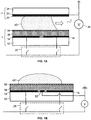
- FIG. 1A is a cross-sectional view of a portion of a conventional digital microfluidic device, showing a two-plate format.
- the device includes a first plate 15 and a second plate 25, separated by a gap 30.
- First plate 25 is formed from an electrically insulating substrate 12, on which an array of digital microfluidic actuation electrodes 14 (e.g. 10 nm Cr+, 100 nm Au) are provided.
- a dielectric layer 16 is formed over actuation electrodes 14 (for example, 2 ⁇ m Parylene-CTM).
- First plate 16 can have more than one dielectric layer.
- Dielectric layer 16 is coated with hydrophobic layer 18 (for example, Teflon AFTM, 50 nm), in order to permit droplet motion under electrical actuation of actuation electrodes 14.
- hydrophobic layer 18 for example, Teflon AFTM, 50 nm
- the hydrophobic surface is often referred to as a working surface.
- Second plate Spaced above actuation electrodes 14 and dielectric layer 16, on the other side of gap 30, is a second plate, where the spacing may be achieved using a spacer (not shown).
- Continuous secondary electrode 22 (or a plurality of secondary electrodes) is provided on an insulating substrate 24 (secondary electrode 22 is often referred to in the digital microfluidic literature as a reference electrode, but the term "secondary" is employed herein in order to avoid confusion with the reference electrode of an electrochemical sensor), and a hydrophobic layer 20 (for example Teflon AFTM, 50 nm) is coated on secondary electrode 22.
- another dielectric layer can be deposited between layers 20, 22.
- Liquid droplets 42 are provided within gap 30 between two hydrophobic layers 18 and 20. Electrodes 14, voltage source 26, and the continuous secondary electrode 22 together form an electric field, digitally manipulated by controller 28. For droplet manipulation, secondary electrode 22 is biased to a potential different from the actuating potential. A commonly used reference potential for secondary electrode 22 is ground.
- the upper hydrophobic layer 20, secondary electrode 22, and substrate layer 24 may be substantially transparent to allow optical detection, such as optical imaging or optical analysis of digital microfluidic assays.
- FIG. 1B shows a one-plate design in which layers 20, 22, and 24 are removed. Rather than have a dedicated secondary electrode layer 22, the secondary electrode is patterned adjacent to electrodes 14, forming a continuous grid 52 separated from electrodes 14 by dielectric material 16. The continuous grid 52 extends in both directions defining the plane in which actuation electrodes 14 are located.
- the design of secondary electrodes 52 is not limited to a grid, e.g. they can be in a form of a wire or an array similarly to electrodes 14.
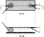
- each sensor comprises a working electrode 110 and counter/pseudo-reference electrode 120 for forming a two-electrode electrochemical cell.
- Counter electrode 120 is provided within a defined spatial region, and working electrode 110 is spatially distributed within the spatial region.
- Each electrochemical electrode has an electrical path extending therefrom, connecting the electrode to an externally addressable contact pad, electrode or electrical connector.
- the electrochemical electrodes may be positioned (e.g. spatially registered) such that when the two-plate device is assembled, the electrochemical electrodes are positioned above (i.e. opposite to) one or more actuation electrodes.
- the two-electrode electrochemical cell is formed from a thin working electrode surrounded by a proportionally larger counter/pseudo-reference electrode.
- Two-electrode cells are easier to fabricate and operate (relative to the more conventional three-electrode cells), but they can suffer from signal instability.
- the area of the counter/pseudo-reference electrode may be designed to be larger than the working electrode, as described in detail below.
- the working electrode is configured as a spatially distributed electrode that spatially extends into the spatial region otherwise occupied by the counter/pseudo-reference electrode.
- working electrode 110 is formed from a number of elongate segments that radiate in a radial configuration from a location near the center of the counter electrode. Such an embodiment increases the contact area between the working electrode and the working solution, making it suitable for sensitive analyses of trace analytes.
- the sensor electrodes may be formed from the same planar electrode material that defines the secondary electrode of the digital microfluidic device.
- the sensor electrodes may be etched on the top plate out of a continuous plate of ITO (using photolithography and wet etching), and separated from the much larger secondary electrode used to enable DMF droplet manipulation.
- the entire top plate may be coated with Teflon-AF, except for the sensor-electrodes, which are exposed, for example, by a lift-off process.
- Various example embodiments provided herein overcome drawbacks associated with known implementations of electrochemical sensors in digital microfluidic devices.
- Prior implementations typically either (a) require complex multistep fabrication processes and are thus likely expensive to manufacture, or (b) simply use external electrodes with no integration, and are thus not suitable for mass production.
- ratio of electrode areas according to various embodiments disclosed herein allow for low detection limits that are likely unmatched by any of the previously reported methods, except for methods relying on fragile nanostructured metal electrodes.
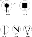
- FIGS. 3A and 3B examples of conventional two-electrode electrochemical sensors are shown, in which the working electrode is not spatially distributed within a spatial region associated with the counter electrode, and is not formed from elongate segments. Such electrode configurations result in the aforementioned performance limitations.
- FIGS. 4A-4C show various example two-electrode electrochemical sensor configurations in which the working electrode is provided as a single elongate segment that is spatially distributed within a spatial region associated with the counter electrode.
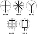
- FIGS. 5A-5E illustrate example two-electrode electrochemical sensor configurations in which the working electrode is provided in the form of a first elongate electrode segment that branches into two or more additional elongate electrode segments that are spatially distributed within a spatial region associated with the counter electrode.
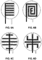
- FIGS. 6A-6D show various example two-electrode electrochemical sensor configurations in which elongate segments of the working electrode are interdigitated with neighbouring elongate segments of the counter electrode.
- the working electrode may be provided as an inwardly directed spiral.
- Another example geometrical configuration of the working electrode is a serpentine configuration.
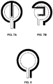
- example two-electrode electrochemical sensor configurations are shown in which the working electrode is provided in the form of an elongate segment that surrounds at least a portion of a perimeter of said electrochemical counter electrode, and also extends within a spatial region associated with the counter electrode.
- FIG. 8 shows an example two-electrode electrochemical sensor configuration in which the working electrode is provided in the form of an elongate segment that surrounds at least a portion of a perimeter of said electrochemical counter electrode.
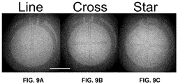
- FIGS. 9A-9C Examples of electrode configurations that have been fabricated and experimentally tested are shown in FIGS. 9A-9C .
- the images show three different two-electrode electrochemical sensors, in the form of a line, cross, and star, that were formed in the top plate of a digital microfluidic device by removal, through etching, of selected regions of an ITO layer.
- the counter electrode can take on a wide variety of other shapes, such as square, elliptical, polygonal, and the like.
- electrochemical sensors based on a two-electrode configuration
- the embodiments provided herein may be adapted or modified to include one or more additional electrodes, such as an electrochemical reference electrode.
- the counter electrode also acts as the reference electrode, simplifying manufacturing and setup process.
- the lack of the third reference electrode removes the ability for it to maintain the accurate potential difference between the counter and working electrode. Therefore, a two-electrode cell with a conventional ratio of the area between the counter electrode and the reference electrode, namely A CE /A WE ⁇ 2 (e.g. as shown in FIGS. 3A and 3B ), will have result in significant noise, as current passing through the system will cover the majority of the surface of the counter electrode, charging the electrode and changing the potential between the counter electrode and the working electrode, and creating a system with a unstable baseline.
- This biased counter electrode is the source of noise that creates the lower signal-to-noise ratio normally seen in conventional two-electrode electrochemical cells.
- the area ratio of the areas of the counter electrode and reference electrode are provide such that 5 ⁇ A CE /A WE ⁇ 15. Within this ratio range, there is sufficient surface area of the counter electrode that normal currents generated by the electrochemical cell are small enough such that they do not charge the counter electrode to a sufficient degree to bias the recording signal.
- an area ratio beyond this range may result in performance degradation for the following reasons: (i) at larger A CE /A WE ratios, too much of the droplet is not exposed to the working electrode, reducing efficiency of the electrochemical cell; and (ii) larger A CE /A WE ratios necessarily require more space on the system, reducing ability to form multiplexed arrays of electrodes and reducing throughput. Notwithstanding these potential problems, embodiments may be realized in which the area ratio exceeds 15, such as an area ratio that exceeds 20, 50, or 100.
- the working electrode is provided as one or more elongate segments, as noted above.
- the width of the elongate segments may be selected, and/or optimized, based on analyte of interest and the desired concentration range.
- the width of at least a portion of one or more segments of the working electrode may be between approximately 1 and 10 microns, between approximately 10 and 100 microns, or between approximately 100 and 500 microns.
- a width in the range of 50-200 microns may be suitable for a wide range of analytes.
- the working electrode is the most sensitive, as normal linear diffusion is replaced by radial diffusion, allowing the electrode to come into contact with a higher amount of analyte at a lower concentration.
- the electrode is most suitable for analytes with low diffusivity or large sizes, these analytes need more time and space to diffuse onto the electrodes.
- ITO is but one example of a suitable conductive material for forming one or both of the electrochemical electrodes.
- conductive materials that may be employed for forming one or both of the electrochemical electrodes include, but are not limited to, gold, silver, carbon and platinum.
- electrochemical electrodes may be formed as gold vs. gold, silver vs. silver, carbon vs. carbon, platinum vs. platinum, and combinations thereamong, such as gold vs. silver, gold vs. platinum, gold vs. carbon, and the like, as will be apparent to one skilled in the art of electrochemical detection.
- such electrodes may be formed on an underlying ITO layer.
- Example methods of fabricating such electrodes on ITO are provided in Shamsi, M.H.; Choi, K.; Ng, A.H.C.; Wheeler, A.R. "A digital microfluidic electrochemical immunoassay” Lab on a Chip 2014, 14, 547-554 .
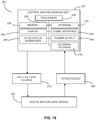
- FIG. 10 an illustration is provided of an example system 200 for controlling digital microfluidic droplet actuation and performing electrochemical measurements.
- the digital microfluidic actuation electrodes, and the secondary electrode are connected to, or connectable, to a high voltage power supply, which is controlled by a controlling and processing unit 225.
- the electrochemical sensing system is controlled by potentiostat 220, which is controlled and/or interrogated by control and processing unit 225.
- high voltage supply 210 and potentiostat 220 are shown as separate system components, it will be understood that two or more system components can be integrated into a single assembly.
- FIG. 10 provides an example implementation of control and processing unit 225, which includes one or more processors 230 (for example, a CPU/microprocessor), bus 232, memory 235, which may include random access memory (RAM) and/or read only memory (ROM), one or more internal storage devices 240 (e.g. a hard disk drive, compact disk drive or internal flash memory), a power supply 245, one more communications interfaces 250, external storage 255, a display 260 and various input/output devices and/or interfaces 265 (e.g., a user input device, such as a keyboard, a keypad, a mouse, a position tracked stylus, a position tracked probe, a foot switch, and/or a microphone for capturing speech commands).
- processors 230 for example, a CPU/microprocessor
- bus 232 includes random access memory (RAM) and/or read only memory (ROM), one or more internal storage devices 240 (e.g. a hard disk drive, compact disk drive or internal flash memory), a power supply 245, one
- bus 232 is depicted as a single connection between all of the components, it will be appreciated that the bus 232 may represent one or more circuits, devices or communication channels which link two or more of the components.
- bus 232 often includes or is a motherboard.
- control and processing unit 225 may be, or include, a general purpose computer or any other hardware equivalents. Control and processing unit 225 may also be implemented as one or more physical devices that are coupled to processor 230 through one of more communications channels or interfaces. For example, control and processing unit 225 can be implemented using application specific integrated circuits (ASICs). Alternatively, control and processing unit 225 can be implemented as a combination of hardware and software, where the software is loaded into the processor from the memory or over a network connection.
- ASICs application specific integrated circuits
- Control and processing unit 225 may be programmed with a set of instructions which when executed in the processor causes the system to perform one or more methods described in the disclosure. Control and processing unit 225 may include many more or less components than those shown.
- a computer readable medium can be used to store software and data which when executed by a data processing system causes the system to perform various methods.
- the executable software and data can be stored in various places including for example ROM, volatile RAM, non-volatile memory and/or cache. Portions of this software and/or data can be stored in any one of these storage devices.
- a machine readable medium includes any mechanism that provides (i.e., stores and/or transmits) information in a form accessible by a machine (e.g., a computer, network device, personal digital assistant, manufacturing tool, any device with a set of one or more processors, etc.).
- Examples of computer-readable media include but are not limited to recordable and non-recordable type media such as volatile and non-volatile memory devices, read only memory (ROM), random access memory (RAM), flash memory devices, floppy and other removable disks, magnetic disk storage media, optical storage media (e.g., compact discs (CDs),digital versatile disks (DVDs), etc.), among others.
- the instructions can be embodied in digital and analog communication links for electrical, optical, acoustical or other forms of propagated signals, such as carrier waves, infrared signals, digital signals, and the like.
- Some aspects of the present disclosure can be embodied, at least in part, in software. That is, the techniques can be carried out in a computer system or other data processing system in response to its processor, such as a microprocessor, executing sequences of instructions contained in a memory, such as ROM, volatile RAM, non-volatile memory, cache, magnetic and optical disks, or a remote storage device. Further, the instructions can be downloaded into a computing device over a data network in a form of compiled and linked version.
- the logic to perform the processes as discussed above could be implemented in additional computer and/or machine readable media, such as discrete hardware components as large-scale integrated circuits (LSI's), application-specific integrated circuits (ASIC's), or firmware such as electrically erasable programmable read-only memory (EEPROM's) and field-programmable gate arrays (FPGAs).
- LSI's large-scale integrated circuits
- ASIC's application-specific integrated circuits
- firmware such as electrically erasable programmable read-only memory (EEPROM's) and field-programmable gate arrays (FPGAs).
- Embodiments of the present disclosure may be employed for a variety of assays that employ electrochemical detection (particularly those that require sensitive analysis of trace amounts of analyte).
- One example application which is illustrated in the examples provided below, involves the sensitive measurement of dopamine concentration using a two-electrode electrochemical sensor that is configured according to the example embodiments disclosed herein. It will be understood that the example application involving dopamine measurement is provided merely as an illustrative example application, and that many other applications may be realized by selecting different analytes (and optionally different electrode compositions).
- the electrochemical electrodes may be formed on the bottom plate, in addition to both the actuation electrodes and the secondary digital microfluidic electrodes.
- electrochemical electrodes may be provided within a region of a single plate that would otherwise have been occupied by a portion of an actuation electrode.
- FIG. 11A shows a cross-sectional view of example single-plate embodiment, where the single plate includes the insulating substrate 12, digital microfluidic actuation electrodes 14, one or more secondary digital microfluidic electrodes (not shown), a dielectric layer 16, and a hydrophobic layer 18.
- the electrochemical working electrode 110 and the counter/pseudo-reference electrode 120 are shown residing on the insulating substrate 12.
- electrochemical electrodes in a two-plate device, can be formed on the bottom plate, coplanar to the actuation electrodes, or in a different plane on the bottom plate, provided that the electrochemical electrodes are in electrical communication with droplets translated on the working surface of the device (e.g. exposed electrodes).
- FIG. 11B illustrates an example two-plate embodiment in which the bottom plate 15 of a two-plate device includes the electrochemical electrodes, and where the top plate 25 includes the top insulating substrate 24, one or more secondary digital microfluidic electrodes 22 (the example embodiment shown includes a single secondary electrode), and a hydrophobic layer 20.
- FIG. 11C illustrates another alternative example two-plate embodiment in which the electrochemical electrodes 110 and 120 are provided in the top plate 25, and where one or more secondary digital microfluidic electrodes (not shown) are provided in the bottom plate 15.
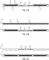
- FIG. 12A plots a comparison of peak current strength compared to total surface area of the working electrode. Note that peak signal current increases -linearly with electrode surface area.
- Representative cyclic voltammograms (CV) are shown in 12B for 2mM ferri-ferrocyanide in PBS buffer for sensors with line, cross and star shaped working electrodes.
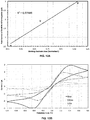
- FIGS. 13A-13C Results from on-chip analysis of dopamine, using two-electrode electrochemical cells formed as described below, are shown in FIGS. 13A-13C .
- FIG. 13A shows background subtracted cyclic voltammograms of dopamine (DA) at 10 ⁇ M.
- the black arrow signifies the potential chosen for comparing peak potentials (0.788V).
- the inset shows the raw signal and background.
- FIG. 13B shows a series of non-background-subtracted cyclic voltammograms of 0, 0.5, 1, 5, and 10 ⁇ M DA.
- FIG. 13A shows background subtracted cyclic voltammograms of dopamine (DA) at 10 ⁇ M.
- the black arrow signifies the potential chosen for comparing peak potentials (0.788V).
- the inset shows the raw signal and background.
- FIG. 13B shows a series of non-background-subtracted cyclic voltammograms of 0, 0.5, 1, 5, and
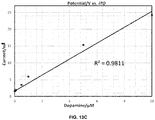
- 13C shows a calibration curve (black) of dopamine from 0 nM to 10 ⁇ M. Error bars represent ⁇ one standard deviation and are smaller than the markers. The limit of detection is 40 nM, defined as the concentration corresponding to three times the standard deviation of blank measurements.
- the use of an all-ITO electroanalytical cell positioned on the top plate makes integration with DMF and microscopy particularly straightforward.
- the patterns were generated by using transparent photomasks printed at 787 dot/mm (20,000 DPI).
- the bottom-plates of DMF devices bearing an array of electrodes were formed by standard photolithography and wet etching. Briefly, chromium- (200 nm thick) and photoresist-coated glass substrates 50.8 mm ⁇ 76.2 mm ⁇ 1.1 mm (2" ⁇ 3" ⁇ 1.1 mm) were exposed to UV light through a photomask using a Suss MicroTec mask aligner (29.8 mW/cm 2 , 10 seconds). The exposed substrates were developed in MF-321 (3 min) and post-baked on a hot plate (125 °C, 1 min). The developed substrates were etched in CR-4 (3 min) and the remaining photoresist was stripped in AZ300T (5 min).
- the substrates were primed for parylene coating by immersing in silane solution (2-propanol, DI water, A-174, and acetic acid 50:50:1:2 v/v/v/v, 10 min) and curing on a hot-plate (80 °C, 10 min).
- silane solution 2-propanol, DI water, A-174, and acetic acid 50:50:1:2 v/v/v/v, 10 min
- devices were coated with ⁇ 7 ⁇ m of Parylene C (vapor deposition) and ⁇ 200 nm of Teflon-AF (spin-coating, 1% w/w in Fluorinert FC-40, 2000 rpm, 60 s), and post-baked on a hot-plate (165 °C, 10 min).
- the polymer coatings were removed from contact pads by gentle scraping with a scalpel.
- Top-plates of DMF devices were formed from indium-tin oxide (ITO) coated glass substrates in three stages.
- ITO indium-tin oxide
- the substrates were sonicated in acetone for 5 min and rinsed in 2-propanol for 1 min. After drying and dehydrating, substrates were spin-coated (3000 RPM, 45 s) with Shipley S1811 photoresist (Marlborough, MA) and then post-baked on a hot plate (95 °C, 2 min). Subsequently, the substrates were exposed (29.8 mW cm -2 , 10 s) through a mask.
- the substrates were developed for 3 min by immersing in MF-321 (MicroChem, Newton, Massachusetts), post-baked on a hot plate (125 °C, 1 min), and then etched for 10 min by immersing in ITO etchant comprising 4 : 2 : 1 (v/v/v) hydrochloric acid, deionized (DI) water, and nitric acid. After rinsing, the remaining photoresist was stripped for 5 min by immersing in AZ300T (Capitol Scientific Inc., Texas).
- the ITO on the device was separated into seven isolated regions, including six electroanalysis electrodes (four 1.6 mm diameter circles and two 1.2 ⁇ 1.2 mm squares) and one large, irregularly shaped DMF driving electrode. Each electroanalysis electrode was connected to a contact pad on the edge of the substrate.
- a spin-coat/lift-off process was performed, as described here in detail.
- ITO-glass slides were immersed in RCA solution (6 : 1 : 1 DI water: 28% aqueous ammonium hydroxide: 30% hydrogen peroxide) for 15 min at 80 °C.
- substrates were spin-coated with Shipley S1811 photoresist (3000 RPM, 60 s) and then post-baked on a hot plate (2 min, 95 °C).
- the substrates were exposed (10 s, 29.8 mW cm -2 ) through a mask bearing features of the two electrochemical electrodes and then developed in MF-321.
- the substrates were flood exposed (10 s, 29.8 mW cm -2 ), and then spin-coated with Teflon-AF and post-baked using the same parameters used for bottom-plate substrates (as above). The substrates were then immersed in acetone with gentle agitation until the Teflon-AF over the patterned sites was lifted off (5-10 s). After rinsing and drying, the Teflon-AF was reflowed by baking on a hot plate at 165 °C and 230 °C for 5 min at each temperature.
Landscapes
- Chemical & Material Sciences (AREA)
- Health & Medical Sciences (AREA)
- Life Sciences & Earth Sciences (AREA)
- Molecular Biology (AREA)
- Chemical Kinetics & Catalysis (AREA)
- General Health & Medical Sciences (AREA)
- Analytical Chemistry (AREA)
- Dispersion Chemistry (AREA)
- Biochemistry (AREA)
- Physics & Mathematics (AREA)
- General Physics & Mathematics (AREA)
- Immunology (AREA)
- Pathology (AREA)
- Electrochemistry (AREA)
- Hematology (AREA)
- Clinical Laboratory Science (AREA)
- Physical Or Chemical Processes And Apparatus (AREA)
- Investigating Or Analyzing Materials By The Use Of Electric Means (AREA)
- Automatic Analysis And Handling Materials Therefor (AREA)
Claims (12)
- Digitale mikrofluidische Vorrichtung, umfassend: eine erste Platte (15), umfassend:ein erstes isolierendes Substrat (12);eine Anordnung von digitalen mikrofluidischen Betätigungselektroden (14), die auf dem ersten isolierenden Substrat bereitgestellt sind;eine erste dielektrische Schicht (16), die über der Anordnung von digitalen mikrofluidischen Betätigungselektroden gebildet ist; undeine erste hydrophobe Schicht (18), die auf der ersten dielektrischen Schicht bereitgestellt ist, wobei die erste hydrophobe Schicht eine erste hydrophobe Arbeitsfläche bereitstellt;eine zweite Platte (25), umfassend:ein zweites isolierendes Substrat (24) mit mindestens einer zweiten hydrophoben Schicht (20), die darauf bereitgestellt ist, wobei die zweite hydrophobe Schicht eine zweite hydrophobe Arbeitsfläche bereitstellt;wobei die erste Platte und die zweite Platte in einer beabstandeten Beziehung vorgesehen sind, die einen Spalt (30) dazwischen definiert, um eine Tropfenbewegung unter Betätigung der Betätigungselektroden zu ermöglichen;wobei eines von dem ersten isolierenden Substrat und dem zweiten isolierenden Substrat eine oder mehrere digitale mikrofluidische Sekundärelektroden (22) aufweist, die darauf bereitgestellt sind, und wobei die eine oder die mehreren digitalen mikrofluidischen Sekundärelektroden bereitgestellt sind, sodass Flüssigkeitströpfchen unter Anlegen von Spannungen zwischen der Anordnung von digitalen mikrofluidischen Betätigungselektroden und der einen oder mehreren digitalen mikrofluidischen Sekundärelektroden transportierbar sind; unddadurch gekennzeichnet, dasseines von dem ersten isolierenden Substrat und dem zweiten isolierenden Substrat einen elektrochemischen Zwei-Elektroden-Sensor mit einer elektrochemischen Arbeitselektrode (110) und einer elektrochemischen Gegen-/Pseudoreferenzelektrode (120) zum Bilden einer elektrochemischen Zelle umfasst, wobei die elektrochemische Arbeitselektrode in Form eines ersten länglichen Elektrodensegments bereitgestellt ist, das in zwei oder mehrere zusätzliche längliche Elektrodensegmente verzweigt, die räumlich innerhalb einer räumlichen Region verteilt sind, die mit der elektrochemischen Gegen-/Pseudoreferenzelektrode assoziiert ist;wobei die elektrochemische Arbeitselektrode und die elektrochemische Gegen-/Pseudoreferenzelektrode an den Spalt zwischen der ersten Platte und der zweiten Platte ausgesetzt sind, sodass ein Tröpfchen, das zwischen der ersten Platte und der zweiten Platte an einer der elektrochemischen Arbeitselektrode und der elektrochemischen Gegen-/Pseudoreferenzelektrode entsprechenden Stelle positioniert ist, in elektrischer Verbindung mit der elektrochemischen Arbeitselektrode und der elektrochemischen Gegen-/Pseudoreferenzelektrode ist; undwobei eine Fläche der elektrochemischen Gegen-/Pseudoreferenzelektrode eine Fläche der elektrochemischen Arbeitselektrode um einen Faktor von mindestens 5 übersteigt.
- Digitale mikrofluidische Vorrichtung nach Anspruch 1, wobei der Faktor, um den die Fläche der elektrochemischen Gegen-/Pseudoreferenzelektrode die Fläche der elektrochemischen Arbeitselektrode überschreitet, weniger als 15 ist.
- Digitale mikrofluidische Vorrichtung nach Anspruch 1, wobei mindestens ein Teil der zwei oder mehreren zusätzlichen länglichen Elektrodensegmente eine Breite zwischen 1 Mikrometer und 10 Mikrometer aufweist.
- Digitale mikrofluidische Vorrichtung nach Anspruch 1, wobei mindestens ein Teil der zwei oder mehreren zusätzlichen länglichen Elektrodensegmente eine Breite zwischen 10 Mikrometer und 100 Mikrometer aufweist.
- Digitale mikrofluidische Vorrichtung nach Anspruch 1, wobei mindestens ein Teil der zwei oder mehreren zusätzlichen länglichen Elektrodensegmente eine Breite zwischen 100 Mikrometer und 500 Mikrometer aufweist.
- Digitale mikrofluidische Vorrichtung nach einem der Ansprüche 3 bis 5, wobei mindestens ein Teil der zwei oder mehreren zusätzlichen länglichen Elektrodensegmente der elektrochemischen Arbeitselektrode mit benachbarten länglichen Segmenten der elektrochemischen Gegen-/Pseudoreferenzelektrode interdigitalisiert ist.
- Digitale mikrofluidische Vorrichtung nach einem der Ansprüche 3 bis 5, wobei mindestens ein Teil der zwei oder mehreren zusätzlichen länglichen Elektrodensegmente als eine einwärts gerichtete Spirale konfiguriert ist.
- Digitale mikrofluidische Vorrichtung nach einem der Ansprüche 3 bis 5, wobei mindestens ein Teil der zwei oder mehreren zusätzlichen länglichen Elektrodensegmente konfiguriert ist, um ein Serpentinenprofil aufzuweisen.
- Digitale mikrofluidische Vorrichtung nach einem der Ansprüche 3 bis 5, wobei das erste längliche Elektrodensegment proximal zu einem zentralen Bereich der elektrochemischen Gegen-/Pseudoreferenzelektrode endet und sich die zwei oder mehreren zusätzlichen länglichen Elektrodensegmente radial von dem ersten länglichen Segment erstrecken.
- Digitale mikrofluidische Vorrichtung nach einem der Ansprüche 1 bis 9, wobei eine oder beide der elektrochemischen Gegen-/Pseudoreferenzelektrode und der elektrochemischen Arbeitselektrode aus dem gleichen leitenden Material wie die digitale mikrofluidische Sekundärelektrode gebildet sind.
- Digitale mikrofluidische Vorrichtung nach Anspruch 10, wobei das leitende Material Indiumzinnoxid ist.
- Digitale mikrofluidische Vorrichtung nach Anspruch 10, wobei die elektrochemische Arbeitselektrode und die elektrochemische Gegen-/Pseudoreferenzelektrode auf dem zweiten isolierenden Substrat gebildet sind.
Applications Claiming Priority (2)
| Application Number | Priority Date | Filing Date | Title |
|---|---|---|---|
| US201462066818P | 2014-10-21 | 2014-10-21 | |
| PCT/CA2015/051066 WO2016061684A1 (en) | 2014-10-21 | 2015-10-21 | Digital microfluidic devices with integrated electrochemical sensors |
Publications (3)
| Publication Number | Publication Date |
|---|---|
| EP3210010A1 EP3210010A1 (de) | 2017-08-30 |
| EP3210010A4 EP3210010A4 (de) | 2018-03-28 |
| EP3210010B1 true EP3210010B1 (de) | 2019-04-24 |
Family
ID=55759989
Family Applications (1)
| Application Number | Title | Priority Date | Filing Date |
|---|---|---|---|
| EP15852188.0A Not-in-force EP3210010B1 (de) | 2014-10-21 | 2015-10-21 | Digitale mikrofluidische vorrichtungen mit integrierten elektrochemischen sensoren |
Country Status (4)
| Country | Link |
|---|---|
| US (1) | US20170315090A1 (de) |
| EP (1) | EP3210010B1 (de) |
| CN (1) | CN107110816B (de) |
| WO (1) | WO2016061684A1 (de) |
Families Citing this family (26)
| Publication number | Priority date | Publication date | Assignee | Title |
|---|---|---|---|---|
| WO2011137533A1 (en) | 2010-05-05 | 2011-11-10 | The Governing Council Of The University Of Toronto | Method of processing dried samples using digital microfluidic device |
| US10464067B2 (en) | 2015-06-05 | 2019-11-05 | Miroculus Inc. | Air-matrix digital microfluidics apparatuses and methods for limiting evaporation and surface fouling |
| WO2016197106A1 (en) | 2015-06-05 | 2016-12-08 | Miroculus Inc. | Evaporation management in digital microfluidic devices |
| JP2020501107A (ja) | 2016-08-22 | 2020-01-16 | ミロキュラス インコーポレイテッド | デジタルマイクロ流体デバイスにおける並行小滴制御のためのフィードバックシステム |
| US20190314820A1 (en) * | 2016-12-08 | 2019-10-17 | University Of Pittsburgh-Of The Commonwealth System Of Higher Education | Digital microfluidic systems for manipulating droplets |
| WO2018126082A1 (en) | 2016-12-28 | 2018-07-05 | Miroculis Inc. | Digital microfluidic devices and methods |
| US11623219B2 (en) | 2017-04-04 | 2023-04-11 | Miroculus Inc. | Digital microfluidics apparatuses and methods for manipulating and processing encapsulated droplets |
| WO2019023133A1 (en) | 2017-07-24 | 2019-01-31 | Miroculus Inc. | DIGITAL MICROFLUIDIC SYSTEMS AND METHODS WITH INTEGRATED PLASMA COLLECTION DEVICE |
| JP7341124B2 (ja) | 2017-09-01 | 2023-09-08 | ミロキュラス インコーポレイテッド | デジタルマイクロ流体デバイスおよびその使用方法 |
| GB2569630B (en) * | 2017-12-21 | 2022-10-12 | Sharp Life Science Eu Ltd | Droplet Interfaces in Electro-wetting Devices |
| CN108226261A (zh) * | 2018-01-02 | 2018-06-29 | 京东方科技集团股份有限公司 | 一种电化学检测芯片及其检测方法 |
| CN108226012B (zh) * | 2018-01-02 | 2021-01-26 | 京东方科技集团股份有限公司 | 微流控芯片、分析装置和微流控芯片的控制方法 |
| WO2019226919A1 (en) | 2018-05-23 | 2019-11-28 | Miroculus Inc. | Control of evaporation in digital microfluidics |
| CN113543883A (zh) | 2019-01-31 | 2021-10-22 | 米罗库鲁斯公司 | 非结垢组合物以及用于操控和处理包封的微滴的方法 |
| WO2020176816A1 (en) | 2019-02-28 | 2020-09-03 | Miroculus Inc. | Digital microfluidics devices and methods of using them |
| CN119158636A (zh) | 2019-04-08 | 2024-12-20 | 米罗库鲁斯公司 | 多盒式数字微流控装置和使用方法 |
| WO2021016614A1 (en) | 2019-07-25 | 2021-01-28 | Miroculus Inc. | Digital microfluidics devices and methods of use thereof |
| EP4061530B1 (de) | 2019-11-20 | 2025-12-10 | Nuclera Ltd | Räumlich variable hydrophobe schichten für digitale mikrofluidik |
| WO2021146573A1 (en) | 2020-01-17 | 2021-07-22 | E Ink Corporation | Spatially variable dielectric layers for digital microfluidics |
| WO2021154627A1 (en) | 2020-01-27 | 2021-08-05 | E Ink Corporation | Method for degassing liquid droplets by electrowetting actuation at higher temperatures |
| WO2021168131A1 (en) | 2020-02-18 | 2021-08-26 | Nuclear Nucleics Ltd. | Adaptive gate driving for high frequency ac driving of ewod arrays |
| TWI795730B (zh) | 2020-02-19 | 2023-03-11 | 英商核酸有限公司 | 用於介電濕潤陣列之高頻交流電驅動的鎖存電晶體驅動 |
| WO2021222061A1 (en) | 2020-04-27 | 2021-11-04 | Nuclera Nucleics Ltd. | Segmented top plate for variable driving and short protection for digital microfluidics |
| CN114585441B (zh) * | 2020-09-29 | 2024-01-23 | 京东方科技集团股份有限公司 | 微流控芯片、文库制备芯片、液滴控制驱动方法 |
| CN112892625B (zh) * | 2021-01-21 | 2022-12-06 | 京东方科技集团股份有限公司 | 一种微流控芯片 |
| US11857961B2 (en) | 2022-01-12 | 2024-01-02 | Miroculus Inc. | Sequencing by synthesis using mechanical compression |
Family Cites Families (7)
| Publication number | Priority date | Publication date | Assignee | Title |
|---|---|---|---|---|
| JP4773360B2 (ja) * | 2003-11-17 | 2011-09-14 | コーニンクレッカ フィリップス エレクトロニクス エヌ ヴィ | 流体を操作するためのシステム |
| GB0414546D0 (en) * | 2004-06-29 | 2004-08-04 | Oxford Biosensors Ltd | Electrode for electrochemical sensor |
| US20090017197A1 (en) * | 2007-07-12 | 2009-01-15 | Sharp Laboratories Of America, Inc. | IrOx nanowire protein sensor |
| US8367370B2 (en) * | 2008-02-11 | 2013-02-05 | Wheeler Aaron R | Droplet-based cell culture and cell assays using digital microfluidics |
| US8696917B2 (en) * | 2009-02-09 | 2014-04-15 | Edwards Lifesciences Corporation | Analyte sensor and fabrication methods |
| CN101609063B (zh) * | 2009-07-16 | 2014-01-08 | 复旦大学 | 一种用于电化学免疫检测的微电极阵列芯片传感器 |
| CN103170383B (zh) * | 2013-03-10 | 2015-05-13 | 复旦大学 | 基于纳米材料电极修饰的电化学集成数字微流控芯片 |
-
2015
- 2015-10-21 WO PCT/CA2015/051066 patent/WO2016061684A1/en not_active Ceased
- 2015-10-21 EP EP15852188.0A patent/EP3210010B1/de not_active Not-in-force
- 2015-10-21 US US15/520,423 patent/US20170315090A1/en not_active Abandoned
- 2015-10-21 CN CN201580055541.7A patent/CN107110816B/zh not_active Expired - Fee Related
Non-Patent Citations (1)
| Title |
|---|
| None * |
Also Published As
| Publication number | Publication date |
|---|---|
| US20170315090A1 (en) | 2017-11-02 |
| CN107110816B (zh) | 2021-06-01 |
| CN107110816A (zh) | 2017-08-29 |
| WO2016061684A1 (en) | 2016-04-28 |
| EP3210010A4 (de) | 2018-03-28 |
| EP3210010A1 (de) | 2017-08-30 |
Similar Documents
| Publication | Publication Date | Title |
|---|---|---|
| EP3210010B1 (de) | Digitale mikrofluidische vorrichtungen mit integrierten elektrochemischen sensoren | |
| US20150377831A1 (en) | Digital microfluidic devices and methods employing integrated nanostructured electrodeposited electrodes | |
| Tzouvadaki et al. | Label-free ultrasensitive memristive aptasensor | |
| Kamath et al. | Three-dimensional carbon interdigitated electrode arrays for redox-amplification | |
| Ng et al. | Highly sensitive reduced graphene oxide microelectrode array sensor | |
| Liu et al. | Microwell device for targeting single cells to electrochemical microelectrodes for high-throughput amperometric detection of quantal exocytosis | |
| CN107449812B (zh) | 一种在cmos标准工艺下的生物化学传感器 | |
| JP4283880B2 (ja) | 電気化学測定用電極板、およびこの電極板を有する電気化学測定装置、ならびにこの電極板を用いて目的物質を定量する方法 | |
| JP5660533B2 (ja) | 電流検出装置 | |
| KR20160086335A (ko) | 나노-갭 전극 쌍 및 이를 제조하는 방법 | |
| Wahl et al. | Electroanalysis at ultramicro and nanoscale electrodes: a comparative study | |
| US9671432B2 (en) | Nanowire electrode sensor | |
| Partel et al. | Lift-off free fabrication approach for periodic structures with tunable nano gaps for interdigitated electrode arrays | |
| US8895340B1 (en) | Biosensor and system and process for forming | |
| KR100563834B1 (ko) | 미세유체 채널이 집적화된 3차원 전극시스템 | |
| Mantis et al. | Suspended highly 3D interdigitated carbon microelectrodes | |
| Halpern et al. | Controlling the sensing properties of silicon nanowires via the bonds nearest to the silicon nanowire surface | |
| Terry et al. | Nanoscale electrode arrays produced with microscale lithographic techniques for use in biomedical sensing applications | |
| JP2017526915A (ja) | センシング装置 | |
| Freisa et al. | Highlighting the impact of blocking monolayers on DNA electrochemical sensors. Theoretical and experimental investigations under flow conditions | |
| Ali et al. | Stencil-based selective surface functionalization of silicon nanowires in 3D device architectures for next-generation biochemical sensors | |
| Raja et al. | Electromigrated gold nanogap tunnel junction arrays: Fabrication and electrical behavior in liquid and gaseous media | |
| US20150168333A1 (en) | Electrochemical affinity sensing chips integrated with fluidic stirring and operation method thereof | |
| JP6061429B2 (ja) | 検体を検出する装置の製造方法 | |
| WO2016176216A1 (en) | Motft and array circuit for chemical/biochemical applications |
Legal Events
| Date | Code | Title | Description |
|---|---|---|---|
| STAA | Information on the status of an ep patent application or granted ep patent |
Free format text: STATUS: THE INTERNATIONAL PUBLICATION HAS BEEN MADE |
|
| PUAI | Public reference made under article 153(3) epc to a published international application that has entered the european phase |
Free format text: ORIGINAL CODE: 0009012 |
|
| STAA | Information on the status of an ep patent application or granted ep patent |
Free format text: STATUS: REQUEST FOR EXAMINATION WAS MADE |
|
| 17P | Request for examination filed |
Effective date: 20170515 |
|
| AK | Designated contracting states |
Kind code of ref document: A1 Designated state(s): AL AT BE BG CH CY CZ DE DK EE ES FI FR GB GR HR HU IE IS IT LI LT LU LV MC MK MT NL NO PL PT RO RS SE SI SK SM TR |
|
| AX | Request for extension of the european patent |
Extension state: BA ME |
|
| DAV | Request for validation of the european patent (deleted) | ||
| DAX | Request for extension of the european patent (deleted) | ||
| A4 | Supplementary search report drawn up and despatched |
Effective date: 20180228 |
|
| RIC1 | Information provided on ipc code assigned before grant |
Ipc: B01L 3/00 20060101ALI20180222BHEP Ipc: G01N 27/403 20060101AFI20180222BHEP |
|
| GRAP | Despatch of communication of intention to grant a patent |
Free format text: ORIGINAL CODE: EPIDOSNIGR1 |
|
| STAA | Information on the status of an ep patent application or granted ep patent |
Free format text: STATUS: GRANT OF PATENT IS INTENDED |
|
| RIC1 | Information provided on ipc code assigned before grant |
Ipc: B01L 3/00 20060101ALI20181026BHEP Ipc: G01N 27/403 20060101AFI20181026BHEP |
|
| INTG | Intention to grant announced |
Effective date: 20181116 |
|
| GRAS | Grant fee paid |
Free format text: ORIGINAL CODE: EPIDOSNIGR3 |
|
| GRAA | (expected) grant |
Free format text: ORIGINAL CODE: 0009210 |
|
| STAA | Information on the status of an ep patent application or granted ep patent |
Free format text: STATUS: THE PATENT HAS BEEN GRANTED |
|
| AK | Designated contracting states |
Kind code of ref document: B1 Designated state(s): AL AT BE BG CH CY CZ DE DK EE ES FI FR GB GR HR HU IE IS IT LI LT LU LV MC MK MT NL NO PL PT RO RS SE SI SK SM TR |
|
| REG | Reference to a national code |
Ref country code: GB Ref legal event code: FG4D |
|
| REG | Reference to a national code |
Ref country code: CH Ref legal event code: EP |
|
| REG | Reference to a national code |
Ref country code: AT Ref legal event code: REF Ref document number: 1124722 Country of ref document: AT Kind code of ref document: T Effective date: 20190515 Ref country code: IE Ref legal event code: FG4D |
|
| REG | Reference to a national code |
Ref country code: DE Ref legal event code: R096 Ref document number: 602015029093 Country of ref document: DE |
|
| REG | Reference to a national code |
Ref country code: NL Ref legal event code: MP Effective date: 20190424 |
|
| REG | Reference to a national code |
Ref country code: LT Ref legal event code: MG4D |
|
| PG25 | Lapsed in a contracting state [announced via postgrant information from national office to epo] |
Ref country code: NL Free format text: LAPSE BECAUSE OF FAILURE TO SUBMIT A TRANSLATION OF THE DESCRIPTION OR TO PAY THE FEE WITHIN THE PRESCRIBED TIME-LIMIT Effective date: 20190424 |
|
| PG25 | Lapsed in a contracting state [announced via postgrant information from national office to epo] |
Ref country code: FI Free format text: LAPSE BECAUSE OF FAILURE TO SUBMIT A TRANSLATION OF THE DESCRIPTION OR TO PAY THE FEE WITHIN THE PRESCRIBED TIME-LIMIT Effective date: 20190424 Ref country code: LT Free format text: LAPSE BECAUSE OF FAILURE TO SUBMIT A TRANSLATION OF THE DESCRIPTION OR TO PAY THE FEE WITHIN THE PRESCRIBED TIME-LIMIT Effective date: 20190424 Ref country code: AL Free format text: LAPSE BECAUSE OF FAILURE TO SUBMIT A TRANSLATION OF THE DESCRIPTION OR TO PAY THE FEE WITHIN THE PRESCRIBED TIME-LIMIT Effective date: 20190424 Ref country code: ES Free format text: LAPSE BECAUSE OF FAILURE TO SUBMIT A TRANSLATION OF THE DESCRIPTION OR TO PAY THE FEE WITHIN THE PRESCRIBED TIME-LIMIT Effective date: 20190424 Ref country code: HR Free format text: LAPSE BECAUSE OF FAILURE TO SUBMIT A TRANSLATION OF THE DESCRIPTION OR TO PAY THE FEE WITHIN THE PRESCRIBED TIME-LIMIT Effective date: 20190424 Ref country code: PT Free format text: LAPSE BECAUSE OF FAILURE TO SUBMIT A TRANSLATION OF THE DESCRIPTION OR TO PAY THE FEE WITHIN THE PRESCRIBED TIME-LIMIT Effective date: 20190824 Ref country code: SE Free format text: LAPSE BECAUSE OF FAILURE TO SUBMIT A TRANSLATION OF THE DESCRIPTION OR TO PAY THE FEE WITHIN THE PRESCRIBED TIME-LIMIT Effective date: 20190424 Ref country code: NO Free format text: LAPSE BECAUSE OF FAILURE TO SUBMIT A TRANSLATION OF THE DESCRIPTION OR TO PAY THE FEE WITHIN THE PRESCRIBED TIME-LIMIT Effective date: 20190724 |
|
| PG25 | Lapsed in a contracting state [announced via postgrant information from national office to epo] |
Ref country code: GR Free format text: LAPSE BECAUSE OF FAILURE TO SUBMIT A TRANSLATION OF THE DESCRIPTION OR TO PAY THE FEE WITHIN THE PRESCRIBED TIME-LIMIT Effective date: 20190725 Ref country code: PL Free format text: LAPSE BECAUSE OF FAILURE TO SUBMIT A TRANSLATION OF THE DESCRIPTION OR TO PAY THE FEE WITHIN THE PRESCRIBED TIME-LIMIT Effective date: 20190424 Ref country code: RS Free format text: LAPSE BECAUSE OF FAILURE TO SUBMIT A TRANSLATION OF THE DESCRIPTION OR TO PAY THE FEE WITHIN THE PRESCRIBED TIME-LIMIT Effective date: 20190424 Ref country code: LV Free format text: LAPSE BECAUSE OF FAILURE TO SUBMIT A TRANSLATION OF THE DESCRIPTION OR TO PAY THE FEE WITHIN THE PRESCRIBED TIME-LIMIT Effective date: 20190424 Ref country code: BG Free format text: LAPSE BECAUSE OF FAILURE TO SUBMIT A TRANSLATION OF THE DESCRIPTION OR TO PAY THE FEE WITHIN THE PRESCRIBED TIME-LIMIT Effective date: 20190724 |
|
| REG | Reference to a national code |
Ref country code: AT Ref legal event code: MK05 Ref document number: 1124722 Country of ref document: AT Kind code of ref document: T Effective date: 20190424 |
|
| PG25 | Lapsed in a contracting state [announced via postgrant information from national office to epo] |
Ref country code: IS Free format text: LAPSE BECAUSE OF FAILURE TO SUBMIT A TRANSLATION OF THE DESCRIPTION OR TO PAY THE FEE WITHIN THE PRESCRIBED TIME-LIMIT Effective date: 20190824 |
|
| REG | Reference to a national code |
Ref country code: DE Ref legal event code: R097 Ref document number: 602015029093 Country of ref document: DE |
|
| PG25 | Lapsed in a contracting state [announced via postgrant information from national office to epo] |
Ref country code: SK Free format text: LAPSE BECAUSE OF FAILURE TO SUBMIT A TRANSLATION OF THE DESCRIPTION OR TO PAY THE FEE WITHIN THE PRESCRIBED TIME-LIMIT Effective date: 20190424 Ref country code: RO Free format text: LAPSE BECAUSE OF FAILURE TO SUBMIT A TRANSLATION OF THE DESCRIPTION OR TO PAY THE FEE WITHIN THE PRESCRIBED TIME-LIMIT Effective date: 20190424 Ref country code: CZ Free format text: LAPSE BECAUSE OF FAILURE TO SUBMIT A TRANSLATION OF THE DESCRIPTION OR TO PAY THE FEE WITHIN THE PRESCRIBED TIME-LIMIT Effective date: 20190424 Ref country code: AT Free format text: LAPSE BECAUSE OF FAILURE TO SUBMIT A TRANSLATION OF THE DESCRIPTION OR TO PAY THE FEE WITHIN THE PRESCRIBED TIME-LIMIT Effective date: 20190424 Ref country code: EE Free format text: LAPSE BECAUSE OF FAILURE TO SUBMIT A TRANSLATION OF THE DESCRIPTION OR TO PAY THE FEE WITHIN THE PRESCRIBED TIME-LIMIT Effective date: 20190424 Ref country code: DK Free format text: LAPSE BECAUSE OF FAILURE TO SUBMIT A TRANSLATION OF THE DESCRIPTION OR TO PAY THE FEE WITHIN THE PRESCRIBED TIME-LIMIT Effective date: 20190424 |
|
| PG25 | Lapsed in a contracting state [announced via postgrant information from national office to epo] |
Ref country code: SM Free format text: LAPSE BECAUSE OF FAILURE TO SUBMIT A TRANSLATION OF THE DESCRIPTION OR TO PAY THE FEE WITHIN THE PRESCRIBED TIME-LIMIT Effective date: 20190424 Ref country code: IT Free format text: LAPSE BECAUSE OF FAILURE TO SUBMIT A TRANSLATION OF THE DESCRIPTION OR TO PAY THE FEE WITHIN THE PRESCRIBED TIME-LIMIT Effective date: 20190424 |
|
| PLBE | No opposition filed within time limit |
Free format text: ORIGINAL CODE: 0009261 |
|
| STAA | Information on the status of an ep patent application or granted ep patent |
Free format text: STATUS: NO OPPOSITION FILED WITHIN TIME LIMIT |
|
| PG25 | Lapsed in a contracting state [announced via postgrant information from national office to epo] |
Ref country code: TR Free format text: LAPSE BECAUSE OF FAILURE TO SUBMIT A TRANSLATION OF THE DESCRIPTION OR TO PAY THE FEE WITHIN THE PRESCRIBED TIME-LIMIT Effective date: 20190424 |
|
| 26N | No opposition filed |
Effective date: 20200127 |
|
| PG25 | Lapsed in a contracting state [announced via postgrant information from national office to epo] |
Ref country code: MC Free format text: LAPSE BECAUSE OF FAILURE TO SUBMIT A TRANSLATION OF THE DESCRIPTION OR TO PAY THE FEE WITHIN THE PRESCRIBED TIME-LIMIT Effective date: 20190424 Ref country code: SI Free format text: LAPSE BECAUSE OF FAILURE TO SUBMIT A TRANSLATION OF THE DESCRIPTION OR TO PAY THE FEE WITHIN THE PRESCRIBED TIME-LIMIT Effective date: 20190424 |
|
| REG | Reference to a national code |
Ref country code: CH Ref legal event code: PL |
|
| PG25 | Lapsed in a contracting state [announced via postgrant information from national office to epo] |
Ref country code: CH Free format text: LAPSE BECAUSE OF NON-PAYMENT OF DUE FEES Effective date: 20191031 Ref country code: LU Free format text: LAPSE BECAUSE OF NON-PAYMENT OF DUE FEES Effective date: 20191021 Ref country code: LI Free format text: LAPSE BECAUSE OF NON-PAYMENT OF DUE FEES Effective date: 20191031 |
|
| REG | Reference to a national code |
Ref country code: BE Ref legal event code: MM Effective date: 20191031 |
|
| PG25 | Lapsed in a contracting state [announced via postgrant information from national office to epo] |
Ref country code: BE Free format text: LAPSE BECAUSE OF NON-PAYMENT OF DUE FEES Effective date: 20191031 |
|
| PG25 | Lapsed in a contracting state [announced via postgrant information from national office to epo] |
Ref country code: IE Free format text: LAPSE BECAUSE OF NON-PAYMENT OF DUE FEES Effective date: 20191021 |
|
| PG25 | Lapsed in a contracting state [announced via postgrant information from national office to epo] |
Ref country code: CY Free format text: LAPSE BECAUSE OF FAILURE TO SUBMIT A TRANSLATION OF THE DESCRIPTION OR TO PAY THE FEE WITHIN THE PRESCRIBED TIME-LIMIT Effective date: 20190424 |
|
| PG25 | Lapsed in a contracting state [announced via postgrant information from national office to epo] |
Ref country code: HU Free format text: LAPSE BECAUSE OF FAILURE TO SUBMIT A TRANSLATION OF THE DESCRIPTION OR TO PAY THE FEE WITHIN THE PRESCRIBED TIME-LIMIT; INVALID AB INITIO Effective date: 20151021 Ref country code: MT Free format text: LAPSE BECAUSE OF FAILURE TO SUBMIT A TRANSLATION OF THE DESCRIPTION OR TO PAY THE FEE WITHIN THE PRESCRIBED TIME-LIMIT Effective date: 20190424 |
|
| PG25 | Lapsed in a contracting state [announced via postgrant information from national office to epo] |
Ref country code: MK Free format text: LAPSE BECAUSE OF FAILURE TO SUBMIT A TRANSLATION OF THE DESCRIPTION OR TO PAY THE FEE WITHIN THE PRESCRIBED TIME-LIMIT Effective date: 20190424 |
|
| PGFP | Annual fee paid to national office [announced via postgrant information from national office to epo] |
Ref country code: FR Payment date: 20221031 Year of fee payment: 8 |
|
| PGFP | Annual fee paid to national office [announced via postgrant information from national office to epo] |
Ref country code: GB Payment date: 20221020 Year of fee payment: 8 Ref country code: DE Payment date: 20221019 Year of fee payment: 8 |
|
| REG | Reference to a national code |
Ref country code: DE Ref legal event code: R119 Ref document number: 602015029093 Country of ref document: DE |
|
| GBPC | Gb: european patent ceased through non-payment of renewal fee |
Effective date: 20231021 |
|
| PG25 | Lapsed in a contracting state [announced via postgrant information from national office to epo] |
Ref country code: GB Free format text: LAPSE BECAUSE OF NON-PAYMENT OF DUE FEES Effective date: 20231021 |
|
| PG25 | Lapsed in a contracting state [announced via postgrant information from national office to epo] |
Ref country code: GB Free format text: LAPSE BECAUSE OF NON-PAYMENT OF DUE FEES Effective date: 20231021 Ref country code: FR Free format text: LAPSE BECAUSE OF NON-PAYMENT OF DUE FEES Effective date: 20231031 Ref country code: DE Free format text: LAPSE BECAUSE OF NON-PAYMENT OF DUE FEES Effective date: 20240501 |