EP3207640B1 - Plug connector for capacitively transmitting data - Google Patents
Plug connector for capacitively transmitting data Download PDFInfo
- Publication number
- EP3207640B1 EP3207640B1 EP15793714.5A EP15793714A EP3207640B1 EP 3207640 B1 EP3207640 B1 EP 3207640B1 EP 15793714 A EP15793714 A EP 15793714A EP 3207640 B1 EP3207640 B1 EP 3207640B1
- Authority
- EP
- European Patent Office
- Prior art keywords
- plug connector
- signal transmission
- connector
- transmission means
- insulating body
- Prior art date
- Legal status (The legal status is an assumption and is not a legal conclusion. Google has not performed a legal analysis and makes no representation as to the accuracy of the status listed.)
- Active
Links
- 230000008054 signal transmission Effects 0.000 claims description 77
- 230000013011 mating Effects 0.000 claims description 63
- 239000004020 conductor Substances 0.000 claims description 34
- 239000003990 capacitor Substances 0.000 claims description 14
- 238000005516 engineering process Methods 0.000 claims description 5
- 238000000034 method Methods 0.000 claims description 5
- 230000005540 biological transmission Effects 0.000 description 10
- 238000007789 sealing Methods 0.000 description 8
- 229910000679 solder Inorganic materials 0.000 description 8
- 230000008878 coupling Effects 0.000 description 7
- 238000010168 coupling process Methods 0.000 description 7
- 238000005859 coupling reaction Methods 0.000 description 7
- 238000013461 design Methods 0.000 description 7
- 238000006073 displacement reaction Methods 0.000 description 5
- 230000001939 inductive effect Effects 0.000 description 5
- 238000009413 insulation Methods 0.000 description 5
- 239000000463 material Substances 0.000 description 3
- RYGMFSIKBFXOCR-UHFFFAOYSA-N Copper Chemical compound [Cu] RYGMFSIKBFXOCR-UHFFFAOYSA-N 0.000 description 2
- 238000010276 construction Methods 0.000 description 2
- 229910052802 copper Inorganic materials 0.000 description 2
- 239000010949 copper Substances 0.000 description 2
- 230000001419 dependent effect Effects 0.000 description 2
- 210000005069 ears Anatomy 0.000 description 2
- 238000003780 insertion Methods 0.000 description 2
- 230000037431 insertion Effects 0.000 description 2
- 239000004033 plastic Substances 0.000 description 2
- 229920003023 plastic Polymers 0.000 description 2
- 238000005476 soldering Methods 0.000 description 2
- 239000000126 substance Substances 0.000 description 2
- 238000012546 transfer Methods 0.000 description 2
- STBLNCCBQMHSRC-BATDWUPUSA-N (2s)-n-[(3s,4s)-5-acetyl-7-cyano-4-methyl-1-[(2-methylnaphthalen-1-yl)methyl]-2-oxo-3,4-dihydro-1,5-benzodiazepin-3-yl]-2-(methylamino)propanamide Chemical compound O=C1[C@@H](NC(=O)[C@H](C)NC)[C@H](C)N(C(C)=O)C2=CC(C#N)=CC=C2N1CC1=C(C)C=CC2=CC=CC=C12 STBLNCCBQMHSRC-BATDWUPUSA-N 0.000 description 1
- MPDDTAJMJCESGV-CTUHWIOQSA-M (3r,5r)-7-[2-(4-fluorophenyl)-5-[methyl-[(1r)-1-phenylethyl]carbamoyl]-4-propan-2-ylpyrazol-3-yl]-3,5-dihydroxyheptanoate Chemical compound C1([C@@H](C)N(C)C(=O)C2=NN(C(CC[C@@H](O)C[C@@H](O)CC([O-])=O)=C2C(C)C)C=2C=CC(F)=CC=2)=CC=CC=C1 MPDDTAJMJCESGV-CTUHWIOQSA-M 0.000 description 1
- 229920002430 Fibre-reinforced plastic Polymers 0.000 description 1
- 229940125878 compound 36 Drugs 0.000 description 1
- 150000001875 compounds Chemical class 0.000 description 1
- 238000013016 damping Methods 0.000 description 1
- 239000000428 dust Substances 0.000 description 1
- 239000012777 electrically insulating material Substances 0.000 description 1
- 230000007613 environmental effect Effects 0.000 description 1
- 239000002360 explosive Substances 0.000 description 1
- 239000011151 fibre-reinforced plastic Substances 0.000 description 1
- 238000001746 injection moulding Methods 0.000 description 1
- 239000011810 insulating material Substances 0.000 description 1
- 238000002955 isolation Methods 0.000 description 1
- 238000004519 manufacturing process Methods 0.000 description 1
- 238000000465 moulding Methods 0.000 description 1
- 230000003287 optical effect Effects 0.000 description 1
- 239000002245 particle Substances 0.000 description 1
- 230000000149 penetrating effect Effects 0.000 description 1
- 230000010287 polarization Effects 0.000 description 1
- 238000004382 potting Methods 0.000 description 1
- 239000000243 solution Substances 0.000 description 1
- 238000010408 sweeping Methods 0.000 description 1
- 238000012360 testing method Methods 0.000 description 1
Images


Classifications
-
- H04B5/72—
-
- H—ELECTRICITY
- H01—ELECTRIC ELEMENTS
- H01R—ELECTRICALLY-CONDUCTIVE CONNECTIONS; STRUCTURAL ASSOCIATIONS OF A PLURALITY OF MUTUALLY-INSULATED ELECTRICAL CONNECTING ELEMENTS; COUPLING DEVICES; CURRENT COLLECTORS
- H01R24/00—Two-part coupling devices, or either of their cooperating parts, characterised by their overall structure
- H01R24/38—Two-part coupling devices, or either of their cooperating parts, characterised by their overall structure having concentrically or coaxially arranged contacts
- H01R24/40—Two-part coupling devices, or either of their cooperating parts, characterised by their overall structure having concentrically or coaxially arranged contacts specially adapted for high frequency
- H01R24/42—Two-part coupling devices, or either of their cooperating parts, characterised by their overall structure having concentrically or coaxially arranged contacts specially adapted for high frequency comprising impedance matching means or electrical components, e.g. filters or switches
-
- H04B5/22—
Definitions
- the invention is based on a connector according to the preamble of independent claim 1.
- the invention also relates to a system comprising a connector and a mating connector.
- Such connectors transmit signals and / or data without the respective signal transmission means being in direct contact with one another.
- Such systems consisting of connectors and mating connectors are used in particular when many mating cycles are to be achieved.
- the signal-transmitting elements are not subject to wear.
- the DE 10 2010 045 742 A1 shows a coupling with means, here coils, for the inductive transmission of data signals.
- the document EP 1 206 012 A1 describes a connector comprising a plug element and a socket element which can be detachably connected to the plug element, for connecting a transmission line to at least one sensor. So that when the plug element and socket element are connected to one another, moisture, dust or dirt particles and aggressive substances penetrating between the plug element and the socket element and aggressive substances do not impair the signal transmission between the plug element and the socket element EP 1 206 012A1 before that the connector has means for realizing a contactless signal transmission between the plug element and the socket element. In particular, inductive, capacitive or optical signal transmission is intended.
- a plug connection according to DE 197 19 730 C1 For a potentially explosive area for energy and data transmission by means of electrical quantities in a bus system, a primary part designed as a transmitter and a secondary part and limiting devices for electrical quantities to be transmitted have.
- the limiter devices are arranged in the primary part and are designed to limit the electrical quantities to be transmitted to the secondary part to values permissible for the respective type of protection.
- the object of the invention is to propose a connector that shows good performance in a wide frequency range and at the same time has a compact design.
- a multi-core cable with at least two or more individual conductors can be connected to the connector according to the invention.
- the connector has at least one signal transmission means, which for contactless signal transmission is provided.
- non-contact signal transmission means that the signal transmission means of a plug connector and a matching mating connector do not physically touch each other.
- Contactless could also mean that there is simply no electrically conductive connection between the signal transmission means.
- the plug connector has a microchip which is connected on the one hand to the signal transmission means or to the signal transmission means and on the other hand can be electrically connected to the individual conductors of the connected cable.
- the signal transmission means are ring capacitors and / or plate capacitors. This enables a space-saving design. In addition, the twist between connector and mating connector is not relevant due to such signal transmission means. The signals are always transmitted equally well.
- the microchip is an active microchip.
- the microchip requires a power supply that is fed, for example, by the incoming conductor. But there can also be a separate power supply, for example a battery, in the connector be provided.
- the microchip can process and forward incoming signals using a so-called multiplexing method. As a result, a large number of incoming conductors and associated signals can be forwarded by only one signal transmission element.
- an inductive signal transmission means is assigned to each incoming conductor. With a multi-core cable, a connector would be very complex.
- the microchip is also able to adapt the transmission power of the signal transmission means, depending on the distance between the connector and the mating connector. This means that it is not necessary to maintain an exact distance between the connector and mating connector.
- the active microchip makes it possible to cover a wide frequency range from binary signals up to high data transfer rates in the megabit range or the associated frequencies.
- the connector has two signal transmission means.
- One signal transmission means is provided for sending the signals arriving at the connector via the connected cable.
- the other signal transmission means is provided for receiving the signals coming in from the mating connector. Thanks to the active microchip, the connector proposed here requires only two signal transmission means, which enables a simple and compact construction of the connector.
- One signal transmission means is designed as a ring capacitor and the other signal transmission means as a circular capacitor plate. This geometry allows the signal transmission means to be plugged into the end face of the connector.
- the ring capacitor and the circular capacitor plate preferably have an equally large surface area.
- the transmission and reception function of the connector according to the invention is thereby optimized.
- the connector according to the invention is insensitive to interference since the signals and / or data are not transmitted by radio.
- the plug connector has a plug connector housing, the end faces of which form a plug side and a connection side.
- the signal transmission means are advantageously completely enclosed by the plug-in side of the housing.
- the signal transmission means or the capacitors described above are arranged on the front side of the connector facing the direction of insertion and are covered there with a plastic material. This is achieved, for example, by an injection molding process. This protects the signal transmission means from environmental influences. This enables the connector to be used in dirty and harsh environments. When unplugged, the individual connector is longitudinally watertight and fulfills protection class IP6x.
- the signal transmission means is preferably aligned on the plug side parallel to the end face of the connector. This enables connectors and mating connectors to optimally exchange signals and data.
- the plug connector has an insulating body which has at least one conductor channel which is electrically connected on one side to the microchip and on the other side can be electrically connected to a conductor of the connected cable.
- the at least one conductor channel is preferably produced using MID technology.
- the number of conductor channels is preferably matched to the number of incoming conductors of the multi-core cable and the signal transmission means. As a rule, several such conductor channels are therefore provided.
- the MID technology enables a compact design of the connector.
- a spring element preferably a spiral spring, is advantageously arranged in the connector housing in such a way that the spring force of the spring element presses the insulating body axially in the plug-in direction of the connector.
- the spring acts on an end face of the insulating body. The other end of the insulating body is thereby pressed to the plug-in side of the connector housing and fits snugly there. As already described above, this end face also has the signal transmission means.
- the respective signal transmission means are aligned parallel to one another when plugged in.
- the signal and data transmission works best.
- the invention also relates to a system of plug-in connectors and mating plug-in connectors, both of which each have at least one signal transmission means, the respective signal transmission means being aligned parallel to one another when plugged in.
- the signal transmission means are preferably at a distance of 1.1 millimeters (mm) or less from one another when plugged in. This distance enables good signal and data transmission.
- connectors and / or the mating connector of the system are ideally designed like the connector claimed according to the invention.
- Connectors and mating connectors can also be constructed identically.
- connectors and mating connectors are also referred to as connectors.
- the connector and the mating connector are preferably connected to one another via a so-called push-pull connection.
- a push-pull connection is particularly ideal for high-frequency applications because of the high level of vibration protection.
- the hermaphroditic design of the insulating body of the connector and mating connector makes it particularly easy to implement a push-pull connection. It is not necessary to pay attention to a special alignment of the mating faces to each other, within the axis of rotation.
- the connector design proposed here allows high mating tolerances.
- the possibly different distance between the signal transmission means can be compensated for by the active chip.
- a system which is operated with a plug connector according to the invention always has a so-called galvanic isolation, since the signal transmission means of the plug and mating plug or socket have no physical contact.
- the Figure 1 shows a connector 1, which is connected (plugged) with a matching mating connector 2 for signal transmission.
- the connector and mating connector shown here is intended for contactless signal transmission.
- the signal transmission takes place here essentially by capacitive means, whereby inductive components can naturally always play a role. The latter, however, play an insignificant role here, if at all.
- the invention explicitly avoids an antenna function of the signal transmission means, in order to ensure, among other things, that the signals / data are secure against eavesdropping.
- the mating connector 2 consists of an insulating body, a housing 4, a cable outlet 5 and a screw sleeve 6.
- the mating area of the mating connector 2 is sealed by a sealing ring 7.
- the insulating body 3 is permanently moved in the direction of the plug-in area with the aid of a spiral spring 8, which is supported on the cable outlet 5 pressed. This ensures that the end face of the insulating body 3 which is relevant for the signal transport is arranged near the plug-in area of the mating connector 2.
- the screw sleeve 6 is fixed to the housing 4 with the aid of fixing plates 9.
- the Figure 3 shows a perspective exploded view of the connector 1. Identical functional parts are provided with the same reference numerals here as with the mating connector 2.
- the insulating body 3 is pressed in the direction of insertion by a spiral spring 8.
- the housing 4 of the connector 1 has an external thread which interacts with an internal thread of the screw sleeve 6 of the mating connector 2 in such a way that the connectors (connector 1 and mating connector 2) are connected to one another and the end faces of the respective insulating bodies 3 are roughly parallel and in a defined manner Are aligned with each other.
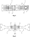
- the Figure 5 shows once the top and once the bottom of the insulating body 3, which is installed in both the connector 1 and the mating connector 2.
- the insulating body 3 has a multiplicity of individual conductor channels 12, which are implemented using MID technology. As a result, the guidance of the channels 12 can be made very flexible, which leads to a small component (insulating body 3).
- Some conductor channels open at a place 11 which is provided for the application of a microchip 10.
- the microchip 10 can process incoming or outgoing data signals as desired.
- the microchip 10 is able to forward the incoming signals using a multiplex method.
- FIGS. 7 to 9 show an alternative embodiment of a connector 1 ', 2' according to the invention.
- Two signal transmission means 13, 14 are introduced into the front of the insulating body 3 '.
- One signal transmission means 13 is ring-shaped and the other signal transmission means 14 is designed as a circular plate.
- Both signal transmission means 13, 14 have the same area dimensions and a connecting element 15 projecting perpendicularly to the basic shape.
- the connecting element 15 is bent to fix the antennas 13, 14 over a fixing surface 16 in the insulating body 3 '.
- the plug 1 ', 2' has a circuit card 17, which in turn has recesses 18.
- the insulating body 3 ' has latching arms 17, which latch in place in the recesses 18 with the insulating body 3' in order to fix the circuit board 17.
- a microchip 10 is applied to the circuit card and is in electrical contact with the signal transmission means 13, 14 and the connected conductors 20.
- the circuit board 17 has so-called solder pads 19, which are provided for the solder connection of the conductor 20 of a (multi-core) cable 21.
- the plug 1 ', 2' has a fixing element 25.
- the fixing element 25 is connected on one side to the printed circuit board 17.
- clamping tabs 24 and a tongue 23 arranged in between are provided on the fixing element, the tongue engaging in a recess 22 in the printed circuit board 17.
- the other side of the fixing element 25 consists of a ring part 26 with fixing arms 27 projecting radially therefrom, which are slightly bent at the ends and pressed against the cable sheath of the connected cable 21 to relieve the cable strain.
- the fixing element also serves to transfer the shield to the connected cable.
- the housing of the connector 1 ', 2' can be designed in different ways.
- the shape of the housing is not relevant to the invention, therefore only the screw part 28 is in Figure 9 shown.
- FIG 10 An elementary component of a third variant of the connector 1 according to the invention can be seen. This is a circular circuit board 29.
- printed circuit boards consist of electrically insulating material with adhering, conductive connections (conductor tracks). Fiber-reinforced plastic is common as an insulating material. The conductor tracks are mostly etched from a thin layer of copper. The components are soldered on so-called soldering pads.
- the first side 29a of the printed circuit board 29 comprises the signal transmission elements which are formed from a copper layer as described above.
- the second side 29b of the circuit board 29 has a mounting location 30 for the microchip 10 already mentioned several times above.
- solder pads 31, clamping points 31 or electrical contacting points 31 for insulation displacement terminals 32 are provided here.
- the insulation displacement contacts 32 are electrically contacted and mechanically fixed.
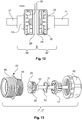
- FIG 11 the components can be seen that together produce the insulating body of the connector 1.
- a cable manager can be seen, which is essentially formed from a cylindrical plastic part.
- holding channels 34 are provided, into which the conductors 20 of the connected cables 21 can be clamped.
- annular contacting element 35 which has recesses into which insulation displacement clamps 32 are inserted.
- the cable manager 33 has fixing arms 36 with window-like openings which cooperate with fixing webs 37 of the contacting element 35 in such a way that these components 33, 34 are fixed to one another.
- the insulation displacement terminals 32 and associated conductor tracks of the printed circuit board 29 (not shown) establish electrical contact between the conductors 20 and the microchip 10.
- the connector 1 consists of a screw head 40 on the cable side.
- a combined sealing and strain relief element 41 is positioned in the screw head 40.
- a wave spring ring 42 is arranged, which essentially fulfills the same task as the spiral spring 8 described above of the first two exemplary embodiments of the connector 1, 1'.
- a double screw head 43 is provided on the plug side, one thread 44 of which can be connected to the screw head 40.
- the opposite thread 45 is provided for fixing with a mating connector.
- Figure 14 shows a perspective view of an insulating body 3 of a first embodiment.
- the insulating body 3 is designed as a flexible printed circuit board, which is folded into itself and in this respect in a side view (see Figure 16 ) has a shape that substantially corresponds to a "T".
- solder pads 19 of the insulating body 3 can also be seen.
- Figure 15 shows a partial view of the insulating body 3 from Figure 14 from a different perspective with two signal transmission means 13, 14.
- the signal transmission means 13, 14 are essentially ring-shaped (signal transmission means 13) or circular (signal transmission means 14), the circular signal transmission means 14 being arranged concentrically with the substantially ring-shaped signal transmission means 13.
- the signal transmission means 13, 14 are arranged on the side of the insulating body 3, which in Figure 14 the opposite to the vertically arranged end part in the illustration opposite.
- Figure 16 shows a side view of two mutually arranged insulating bodies 3 of the first embodiment.
- the insulating bodies 3 each have a shape in the side view which essentially corresponds to a "T", the respective insulating body 3 being folded over itself in one half of the sweeping bar of the "T".
- the microchip 10 is arranged in each of these folding areas, and is therefore located opposite the signal transmission means 13, 14.
- Figure 17 is a view of connector 1 '"and mating connector 2'" of the first embodiment.
- Figure 18 is a perspective view of an insulating body 3 'of a second embodiment.
- the insulating body 3 ' is designed as a flexible printed circuit board
- the in Figure 18 Insulating body 3 'shown instead of in example Figure 14 recognizable folded area of the insulating body shown there has an essentially tubular area, on each of which ring-shaped signal transmission means 13 'and 14' are provided.
- Figure 18 shows a perspective view of another insulating body 3 "of the second exemplary embodiment.
- the basic structure of the insulating body 3" essentially corresponds to the insulating body 3 'of FIG Figure 18 is shown, but the signal transmission means 13 ", 14", which are also strip-shaped and bent into rings, are arranged on the inside of the tubular part of the insulating body 3 ", while the signal transmission means 13 ', 14' of the insulating body 3 'extend Figure 18 located on the outside of the tubular area.
- Figure 20 shows a side view of two mutually arranged insulating bodies 3 ', 3 "of the second exemplary embodiment Figure 20 can be seen, the insulating body 3 ', 3 ", which in Figure 18 and 19 are shown for coupling to one another in the form of a male coupling element (see Figure 18 ) and a female coupling element (see Figure 19 ) designed.
- the signal transmission means 13 ', 14' and 13 ", 14" are opposite each other, however, without direct contact being provided.
- the signal transmission means 13', 13", 14 ', 14 " can also each be on the outside or inside of the tubular part of the insulating body 3', 3 "be arranged. If the flexible printed circuit board is sufficiently thin, a reversal can also be made in that the female coupling component carries its signal transmission means on the outside and the male coupling component carries its signal transmission means on the inside.
- Figure 21 shows a view of connector 1 "" and mating connector 2 "" of the second embodiment. For further details, see the Figures 25 , 32 and 33 referred.
- Figures 22 to 24 each show partial views of an insulating body 3 of the first or second embodiment.
- the insulating body 3 which is designed in the form of a flexible printed circuit board, has conductor tracks 46 on both sides, with which overall space savings can be achieved. In order to enable adequate contacting, through holes 47 are provided so that a conductor track 46 is connected to a corresponding conductor track 46 on the opposite side of the insulating body 3.
- Figure 25 shows a perspective view of an insulating body 3 'of the second embodiment with a cable connector 48 attached to it.
- One way of contacting the solder pads 19 with the conductors of the cable is to attach a cable connector, for example an H-Flex SMT connector, to which a corresponding cable connector mating connector can then be coupled, with which the Head of the cable 21 are connected.
- a cable connector for example an H-Flex SMT connector
- Figure 26 shows a perspective view of an insulating body 3 of the first embodiment with attached cable connector 48, 49 with connected cable 21.
- the cable 21 is attached directly or indirectly to the insulating body 3, 3 ', 3 "of the first or second exemplary embodiment, the cable and the insulating body can be cast together in a suitable material, so that a desired sealing of the overall arrangement can be achieved offers protection against the influence of moisture or similar.
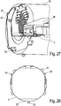
- Figure 27 and Figure 28 are views illustrating an embedding of the insulating body 3 of the first embodiment.
- the insulating body 3 with attached cable connector 48 which is enclosed in a sealing compound 50.
- the insulating body 3 has holding ears 51 which, in the form of embedding, make it possible to fix the end region of the insulating body 3 in the desired manner, in particular in such a way that there is sufficient parallelism with the end face.
- Recesses 2 which can also be recognized, result from the provision of corresponding wall projections in the form through which the end region of the insulating body 3 is pressed against the molding surface.
- the holding ears 51 of the insulating body 3 are also in Figure 28 to recognize.
- bayonet buttons 53 are provided when forming the potting compound.
- FIGS 29, 30 and 31 show perspective views of the connector 1 '"and the mating connector 2'" of the first embodiment.
- the in Figure 29 shown mating connector 2 '"bayonet knobs 53 during the in Figure 30 has shown connector 1 '"on a corresponding projecting part bayonet slots 54, in which the bayonet buttons 53 can engage in order to achieve a fixation of connector 1" and mating connector 2 "" to each other, as shown in Figure 31 is shown.
- Figure 32 and Figure 33 show perspective views of the connector 1 "" and the mating connector 2 "" of the second embodiment.
- the insulating body of the connector 1 '"and the insulating body of the mating connector 2" are each sealed in a suitable manner, the sealing in the case of the connector 1" “having a longitudinal slot, which allows flexibility with regard to deformation to widen the annular area
- the connector 1 "" has an annular projection in the end region which runs around on the inside.
- the mating connector 2 "" has an annular groove 57 at a corresponding point with which the ring projection 56 can be brought into engagement in order to achieve a certain fixation of the connector 1 "" and mating connector 2 "" with one another.
Description
Die Erfindung geht aus von einem Steckverbinder nach dem Oberbegriff des unabhängigen Anspruchs 1. Die Erfindung bezieht sich ebenfalls auf ein System aus einem Steckverbinder und einem Gegensteckverbinder.The invention is based on a connector according to the preamble of
Derartige Steckverbinder übermitteln Signale und/oder Daten, ohne dass die jeweiligen Signalübertragungsmittel in direktem Kontakt zueinander stehen. Derartige Systeme aus Steckverbinder und Gegensteckverbinder werden insbesondere dann eingesetzt, wenn viele Steckzyklen erreicht werden sollen. Die signalübertragenden Elemente unterliegen keinem Verschleiß.Such connectors transmit signals and / or data without the respective signal transmission means being in direct contact with one another. Such systems consisting of connectors and mating connectors are used in particular when many mating cycles are to be achieved. The signal-transmitting elements are not subject to wear.
Die Signalübertragung mithilfe von induktiv und/oder kapazitiv wirkenden Signalübertragungsmitteln ist bekannt. Die
Die hier vorgeschlagene Technik ist aber zu groß bauend, um sie in kleineren Steckverbindern einzusetzen. In vielen Anwendungen werden oft kleine und kompakte Steckverbinder benötigt.However, the technology proposed here is too large to be used in smaller connectors. Small and compact connectors are often required in many applications.
Das Dokument
Eine Steckverbindung gemäß
Die Aufgabe der Erfindung besteht darin, einen Steckverbinder vorzuschlagen, der eine gute Leistungsfähigkeit in einem weiten Frequenzbereich zeigt und gleichzeitig eine kompakte Bauweise aufweist.The object of the invention is to propose a connector that shows good performance in a wide frequency range and at the same time has a compact design.
Die Aufgabe wird durch die kennzeichnenden Merkmale des unabhängigen Anspruchs 1 gelöst.The object is achieved by the characterizing features of
Vorteilhafte Ausgestaltungen der Erfindung sind in den Unteransprüchen angegeben.Advantageous embodiments of the invention are specified in the subclaims.
An den erfindungsgemäßen Steckverbinder kann ein mehradriges Kabel mit zumindest zwei oder mehr einzelnen Leitern angeschlossen werden. Der Steckverbinder weist zumindest ein Signalübertragungsmittel auf, welches zur berührungslosen Signalübertragung vorgesehen ist. Berührungslose Signalübertragung bedeutet in diesem Fall, dass sich die Signalübertragungsmittel von einem Steckverbinder und einem dazu passenden Gegensteckverbinder physikalisch nicht berühren. Berührungslos könnte auch bedeuten, dass lediglich keine elektrisch leitende Verbindung zwischen den Signalübertragungsmitteln besteht.A multi-core cable with at least two or more individual conductors can be connected to the connector according to the invention. The connector has at least one signal transmission means, which for contactless signal transmission is provided. In this case, non-contact signal transmission means that the signal transmission means of a plug connector and a matching mating connector do not physically touch each other. Contactless could also mean that there is simply no electrically conductive connection between the signal transmission means.
Der Steckverbinder weist einen Mikrochip auf, der einerseits mit dem Signalübertragungsmittel oder mit den Signalübertragungsmitteln verbunden ist und andererseits mit den einzelnen Leitern des angeschlossenen Kabels elektrisch verbindbar ist.The plug connector has a microchip which is connected on the one hand to the signal transmission means or to the signal transmission means and on the other hand can be electrically connected to the individual conductors of the connected cable.
Es handelt sich bei den Signalübertragungsmitteln um Ringkondensatoren und/oder Plattenkondensatoren. Dadurch ist eine platzsparende Bauweise möglich. Außerdem ist durch derlei Signalübertragungsmittel die Verdrehung zwischen Steckverbinder und Gegensteckverbinder nicht relevant. Die Signale werden immer gleich gut übertragen.The signal transmission means are ring capacitors and / or plate capacitors. This enables a space-saving design. In addition, the twist between connector and mating connector is not relevant due to such signal transmission means. The signals are always transmitted equally well.
Bei dem Mikrochip handelt es sich um einen aktiven Mikrochip. Der Mikrochip benötigt eine Stromversorgung, die beispielsweise durch die eingehenden Leiter gespeist wird. Es kann aber auch eine separate Stromversorgung, beispielsweise eine Batterie, im Steckverbinder vorgesehen sein. Der Mikrochip kann eingehende Signale nach einem so genannten Multiplexingverfahren verarbeiten und weiterleiten. Dadurch können eine Vielzahl von eingehenden Leitern und zugehörigen Signalen durch lediglich ein Signal-übertragungselement weitergeleitet werden. Bei der
Der Mikrochip ist außerdem in der Lage die Sendeleistung der Signalübertragungsmittel, je nach Abstand von Steckverbinder und Gegensteckverbinder, anzupassen. Dadurch ist es nicht notwendig einen exakten Abstand zwischen Steckverbinder und Gegensteckverbinder einzuhalten.The microchip is also able to adapt the transmission power of the signal transmission means, depending on the distance between the connector and the mating connector. This means that it is not necessary to maintain an exact distance between the connector and mating connector.
Durch den aktiven Mikrochip ist es möglich einen weiten Frequenzbereich von binären Signalen bis hin zu hohen Datenübertragungsraten im Megabitbereich bzw. den zugehörigen Frequenzen abzudecken.The active microchip makes it possible to cover a wide frequency range from binary signals up to high data transfer rates in the megabit range or the associated frequencies.
Durch den aktiven Chip gibt es bei der Signal- oder Datenübertragung keine frequenzabhängige Dämpfung, da aktiv angesteuerte Kondensatoren (als Datenübertragungsmittel) kein Tief-, Hoch- oder Bandpassverhalten zeigen. Eine aktiv betriebene kapazitive Kopplung, wie sie hier vorgeschlagen wird, zeigt keine frequenzabhängige Dämpfung, was dem Steckverbinder ein breites Einsatzgebiet eröffnet.Due to the active chip, there is no frequency-dependent attenuation in signal or data transmission, since actively controlled capacitors (as data transmission means) show no low, high or bandpass behavior. An actively operated capacitive coupling, as proposed here, shows no frequency-dependent damping, which opens up a wide range of applications for the connector.
Der Steckverbinder weist zwei Signalübertragungsmittel auf. Das eine Signalübertragungsmittel ist zum Senden der am Steckverbinder, über das angeschlossene Kabel, eingehenden Signale vorgesehen. Das andere Signalübertragungsmittel ist zum Empfang der vom Gegenstecker eingehenden Signale vorgesehen. Der hier vorgeschlagene Steckverbinder kommt dank des aktiven Mikrochips mit lediglich zwei Signalübertragungsmitteln aus, was eine einfache und kompakte Bauweise des Steckverbinders ermöglicht.The connector has two signal transmission means. One signal transmission means is provided for sending the signals arriving at the connector via the connected cable. The other signal transmission means is provided for receiving the signals coming in from the mating connector. Thanks to the active microchip, the connector proposed here requires only two signal transmission means, which enables a simple and compact construction of the connector.
Ein Signalübertragungsmittel ist als Ringkondensator und das andere Signalübertragungsmittel als kreisförmige Kondensatorplatte ausgebildet. Diese Geometrie erlaubt es die Signalübertragungsmittel steckseitig in die Stirnfläche des Steckverbinders zu integrieren.One signal transmission means is designed as a ring capacitor and the other signal transmission means as a circular capacitor plate. This geometry allows the signal transmission means to be plugged into the end face of the connector.
Vorzugsweise weisen der Ringkondensator und die kreisförmige Kondensatorplatte eine gleich große Oberfläche auf. Dadurch wird die Sende- und Empfangsfunktion des erfindungsgemäßen Steckverbinders optimiert.The ring capacitor and the circular capacitor plate preferably have an equally large surface area. The transmission and reception function of the connector according to the invention is thereby optimized.
Der erfindungsgemäße Steckverbinder ist Störunempfindlich, da die Signale und/oder Daten nicht per Funk übertragen werden.The connector according to the invention is insensitive to interference since the signals and / or data are not transmitted by radio.
Der Steckverbinder weist ein Steckverbindergehäuse auf, dessen Stirnflächen eine Steckseite und eine Anschlussseite bilden. Vorteilhafterweise sind die Signalübertragungsmittel von der Steckseite des Gehäuses vollständig umschlossen. Oder anders gesagt sind die Signalübertragungsmittel beziehungsweise die oben beschriebenen Kondensatoren an der zur Steckrichtung weisenden Stirnseite des Steckverbinders angeordnet und dort mit einem Kunststoffmaterial überzogen. Dies wird beispielswiese durch einen Spritzgussprozess realisiert. Hierdurch sind die Signalübertragungsmittel vor Umwelteinflüssen geschützt. Dadurch kann der Steckverbinder in schmutzigen und rauen Umgebungen eingesetzt werden. Im ungesteckten Zustand ist der einzelne Steckverbinder längswasserdicht und erfüllt die Schutzklasse IP6x.The plug connector has a plug connector housing, the end faces of which form a plug side and a connection side. The signal transmission means are advantageously completely enclosed by the plug-in side of the housing. In other words, the signal transmission means or the capacitors described above are arranged on the front side of the connector facing the direction of insertion and are covered there with a plastic material. This is achieved, for example, by an injection molding process. This protects the signal transmission means from environmental influences. This enables the connector to be used in dirty and harsh environments. When unplugged, the individual connector is longitudinally watertight and fulfills protection class IP6x.
Vorzugsweise ist das Signalübertragungsmittel steckseitig parallel zur Stirnfläche des Steckverbinders ausgerichtet. Dadurch können Steckverbinder und Gegensteckverbinder optimal Signale beziehungsweise Daten austauschen.The signal transmission means is preferably aligned on the plug side parallel to the end face of the connector. This enables connectors and mating connectors to optimally exchange signals and data.
Besonders vorteilhaft ist es, wenn der Steckverbinder einen Isolierkörper aufweist, der zumindest einen Leiterkanal aufweist, der einseitig elektrisch mit dem Mikrochip verbunden ist und anderseitig elektrisch mit einem Leiter des angeschlossenen Kabels verbindbar ist. Vorzugsweise ist der zumindest eine Leiterkanal mithilfe der MID-Technik hergestellt. Die Anzahl der Leiterkanäle wird vorzugsweise auf die Anzahl der eingehenden Leiter des mehradrigen Kabels und der Signalübertragungsmittel abgestimmt. In der Regel sind daher mehrere solcher Leiterkanäle vorgesehen. Die MID-Technik ermöglicht eine kompakte Bauweise des Steckverbinders.It is particularly advantageous if the plug connector has an insulating body which has at least one conductor channel which is electrically connected on one side to the microchip and on the other side can be electrically connected to a conductor of the connected cable. The at least one conductor channel is preferably produced using MID technology. The number of conductor channels is preferably matched to the number of incoming conductors of the multi-core cable and the signal transmission means. As a rule, several such conductor channels are therefore provided. The MID technology enables a compact design of the connector.
Vorteilhafterweise ist im Steckverbindergehäuse ein Federelement, vorzugsweise eine Spiralfeder, derart angeordnet, dass die Federkraft des Federelements den Isolierkörper axial in Steckrichtung des Steckverbinders drückt. Die Feder wirkt dabei auf eine Stirnseite des Isolierkörpers ein. Das andere Ende des Isolierkörpers wird dadurch zur Steckseite des Steckverbindergehäuses gepresst und liegt dort eng an. Wie bereits oben beschrieben weist diese Stirnseite auch die Signalübertragungsmittel auf.A spring element, preferably a spiral spring, is advantageously arranged in the connector housing in such a way that the spring force of the spring element presses the insulating body axially in the plug-in direction of the connector. The spring acts on an end face of the insulating body. The other end of the insulating body is thereby pressed to the plug-in side of the connector housing and fits snugly there. As already described above, this end face also has the signal transmission means.
Idealerweise sind die jeweiligen Signalübertragungsmittel im gesteckten Zustand parallel zueinander ausgerichtet. Die Signal- bzw. Datenübertragung funktioniert so am besten.Ideally, the respective signal transmission means are aligned parallel to one another when plugged in. The signal and data transmission works best.
Die Erfindung bezieht sich ebenfalls auf ein System aus Steckverbinder und Gegensteckverbinder, die beide jeweils zumindest ein Signalübertragungsmittel aufweisen, wobei die jeweiligen Signalübertragungsmittel im gesteckten Zustand parallel zueinander ausgerichtet sind.The invention also relates to a system of plug-in connectors and mating plug-in connectors, both of which each have at least one signal transmission means, the respective signal transmission means being aligned parallel to one another when plugged in.
Vorzugsweise haben die Signalübertragungsmittel im gesteckten Zustand einen Abstand von 1,1 Millimeter (mm) oder weniger zueinander. Diese Entfernung ermöglicht eine gute Signal- bzw. Datenübertragung.The signal transmission means are preferably at a distance of 1.1 millimeters (mm) or less from one another when plugged in. This distance enables good signal and data transmission.
Der Steckverbinder und/oder der Gegensteckverbinder des Systems sind idealerweise wie der erfindungsgemäß beanspruchte Steckverbinder ausgeführt. Steckverbinder und Gegensteckverbinder können auch baugleich ausgeführt sein. Im Folgenden werden Steckverbinder und Gegensteckverbinder auch als Stecker bezeichnet.The connector and / or the mating connector of the system are ideally designed like the connector claimed according to the invention. Connectors and mating connectors can also be constructed identically. In the following, connectors and mating connectors are also referred to as connectors.
Vorzugsweise sind der Steckverbinder und der Gegensteckverbinder über eine so genannte Push-Pull-Verbindung miteinander verbunden sind. Eine Push-Pull-Verbindung ist besonders bei Hochfrequenzanwendungen ideal, da ein hoher Vibrationsschutz besteht. Durch das hermaphroditische Design der Isolierkörper von Stecker und Gegenstecker kann eine Push-Pull-Verbindung besonders einfach realisiert werden. Es muss nicht auf eine spezielle Ausrichtung der Steckgesichter zueinander, innerhalb der Drehachse, geachtet werden.The connector and the mating connector are preferably connected to one another via a so-called push-pull connection. A push-pull connection is particularly ideal for high-frequency applications because of the high level of vibration protection. The hermaphroditic design of the insulating body of the connector and mating connector makes it particularly easy to implement a push-pull connection. It is not necessary to pay attention to a special alignment of the mating faces to each other, within the axis of rotation.
Es ist aber auch denkbar eine Schraubverbindung, eine Bajonettverriegelung, eine Verriegelung über einen Verriegelungsbügel oder Vergleichbares vorzusehen. Das hermaphroditische Design von Stecker und Gegenstecker ermöglicht hier eine Vielzahl von Lösungen.However, it is also conceivable to provide a screw connection, a bayonet lock, a lock via a locking bracket or the like. The hermaphroditic design of the connector and mating connector enables a multitude of solutions.
Durch das hermaphroditische Design ist es außerdem nicht notwendig, den Steckverbinder mit mechanischen Polarisationsmitteln zu versehen.Thanks to the hermaphroditic design, it is also not necessary to provide the connector with mechanical polarization means.
Das hier vorgeschlagene Steckverbinderdesign lässt hohe Stecktoleranzen zu. Die ggf. unterschiedliche Entfernung zwischen den Signalübertragungsmitteln kann durch den aktiven Chip ausgeglichen werden.The connector design proposed here allows high mating tolerances. The possibly different distance between the signal transmission means can be compensated for by the active chip.
Ein System, welches mit einem erfindungsgemäßen Steckverbinder betrieben wird, weist immer eine so genannte galvanische Trennung auf, da die Signalübertragungsmittel von Stecker und Gegenstecker bzw. Buchse keinen physikalischen Kontakt haben.A system which is operated with a plug connector according to the invention always has a so-called galvanic isolation, since the signal transmission means of the plug and mating plug or socket have no physical contact.
Ausführungsbeispiele der Erfindung sind in den Zeichnungen dargestellt und werden im Folgenden näher erläutert. Es zeigen:
- Fig. 1
- eine Seitenansicht eines Systems von einem Steckverbinder und Gegensteckverbinder,
- Fig. 2
- eine perspektivische Explosionszeichnung des Gegensteckverbinders,
- Fig. 3
- eine perspektivische Explosionszeichnung des Steckverbinders,
- Fig. 4
- eine perspektivische Schnittdarstellung des Systems von Steckverbinder und Gegensteckverbinder,
- Fig. 5
- eine Draufsicht eines Isolierkörpers des Steckverbinders und/oder des Gegensteckverbinders auf die Ober- und auf die Unterseite,
- Fig. 6
- eine Seitenansicht des Isolierkörpers des Steckverbinders und/oder des Gegensteckverbinders,
- Fig. 7
- eine weitere Ausführungsform und hier insbesondere eine perspektivische Darstellung eines Steckbereichs des Steckverbinders,
- Fig. 8
- eine perspektivische Darstellung des Steckbereichs des Steckverbinders mit einer Kabelzugentlastung,
- Fig. 9
- eine perspektivische Darstellung eines weiteren Steckverbinders und/oder Gegensteckverbinders mit angeschlossenem Kabel,
- Fig. 10
- eine weitere Ausführungsform und hier insbesondere eine beidseitige Ansicht einer Leiterplatte desselben,
- Fig. 11
- eine perspektivische Darstellung von Bauteilen, die einen Isolierkörper des Steckverbinders bilden,
- Fig. 12
- eine Seitenansicht von den Isolierkörpern von Steckverbinder und Gegensteckverbinder,
- Fig. 13
- eine perspektivische Explosionszeichnung eines Ausführungsbeispiels des Steckverbinders,
- Fig. 14
- eine perspektivische Ansicht eines Isolierkörpers eines ersten Ausführungsbeispiels,
- Fig. 15
- eine Teilansicht des Isolierkörpers aus
Figur 14 aus anderer Perspektive mit zwei Signalübertragungsmitteln, - Fig. 16
- eine Seitenansicht von zwei zueinander angeordneten Isolierkörpern des ersten Ausführungsbeispiels,
- Fig. 17
- eine Ansicht von Steckverbinder und Gegensteckverbinder des ersten Ausführungsbeispiels,
- Fig. 18
- eine perspektivische Ansicht eines Isolierkörpers eines zweiten Ausführungsbeispiels,
- Fig. 19
- eine perspektivische Ansicht eines anderen Isolierkörpers des zweiten Ausführungsbeispiels,
- Fig. 20
- eine Seitenansicht von zwei zueinander angeordneten Isolierkörpern des zweiten Ausführungsbeispiels,
- Fig. 21
- eine Ansicht von Steckverbinder und Gegensteckverbinder des zweiten Ausführungsbeispiels,
- Fig. 22
bis 24 - Teilansichten eines Isolierkörpers des ersten oder zweiten Ausführungsbeispiels,
- Fig. 25
- eine perspektivische Ansicht eines Isolierkörpers des zweiten Ausführungsbeispiels mit daran angebrachtem Kabelanschlussstecker,
- Fig. 26
- eine perspektivische Ansicht eines Isolierkörpers des ersten Ausführungsbeispiels mit daran angebrachtem Kabelanschlussstecker mit angeschlossenem Kabel,
- Fig. 27 und 28
- Ansichten zur Illustration eines Einbettens des Isolierkörpers des ersten Ausführungsbeispiels,
- Fig. 29, 30
und 31 - perspektivische Ansichten des Steckverbinders und des Gegensteckverbinders des ersten Ausführungsbeispiels, und
- Fig. 32
und 33 - perspektivische Ansichten des Steckverbinders und Gegensteckverbinders des zweiten Ausführungsbeispiels.
- Fig. 1
- a side view of a system of a connector and mating connector,
- Fig. 2
- a perspective exploded view of the mating connector,
- Fig. 3
- a perspective exploded view of the connector,
- Fig. 4
- 2 shows a perspective sectional illustration of the system of plug connector and mating plug connector,
- Fig. 5
- a plan view of an insulating body of the connector and / or the mating connector on the top and on the bottom,
- Fig. 6
- a side view of the insulating body of the connector and / or the mating connector,
- Fig. 7
- another embodiment and here in particular a perspective view of a plug-in area of the connector,
- Fig. 8
- a perspective view of the plug area of the connector with a cable strain relief,
- Fig. 9
- 2 shows a perspective illustration of a further connector and / or mating connector with a connected cable,
- Fig. 10
- another embodiment and here in particular a two-sided view of a circuit board of the same,
- Fig. 11
- 3 shows a perspective illustration of components which form an insulating body of the plug connector,
- Fig. 12
- a side view of the insulating bodies of connectors and mating connectors,
- Fig. 13
- 2 shows a perspective exploded drawing of an exemplary embodiment of the connector,
- Fig. 14
- 2 shows a perspective view of an insulating body of a first exemplary embodiment,
- Fig. 15
- a partial view of the insulating body
Figure 14 from a different perspective with two signal transmission means, - Fig. 16
- 2 shows a side view of two mutually arranged insulating bodies of the first exemplary embodiment,
- Fig. 17
- 2 shows a view of the connector and mating connector of the first exemplary embodiment,
- Fig. 18
- 2 shows a perspective view of an insulating body of a second exemplary embodiment,
- Fig. 19
- 2 shows a perspective view of another insulating body of the second exemplary embodiment,
- Fig. 20
- 2 shows a side view of two mutually arranged insulating bodies of the second exemplary embodiment,
- Fig. 21
- 2 shows a view of the connector and mating connector of the second exemplary embodiment,
- 22 to 24
- Partial views of an insulating body of the first or second embodiment,
- Fig. 25
- 2 shows a perspective view of an insulating body of the second exemplary embodiment with a cable connector plug attached to it,
- Fig. 26
- 2 shows a perspective view of an insulating body of the first exemplary embodiment with a cable connector plug connected thereto with a connected cable,
- 27 and 28
- Views to illustrate an embedding of the insulating body of the first embodiment,
- 29, 30 and 31
- perspective views of the connector and the mating connector of the first embodiment, and
- 32 and 33
- perspective views of the connector and mating connector of the second embodiment.
Die Figuren enthalten teilweise vereinfachte, schematische Darstellungen. Zum Teil werden für gleiche, aber gegebenenfalls nicht identische Elemente identische Bezugszeichen verwendet. Verschiedene Ansichten gleicher Elemente könnten unterschiedlich skaliert sein.The figures contain partially simplified, schematic representations. In some cases, identical reference numerals are used for identical but possibly not identical elements. Different views of the same elements could be scaled differently.
Die
In der
Die
In der Schnittfigur 4 ist die Funktion der Spiralfeder 8 gut zu erkennen. Beide Isolierkörper 3 werden zum Steckbereich des jeweiligen Steckers 1, 2 bis hin zu einem Anschlag gedrückt.The function of the
Die
In
Die
Der Stecker 1', 2' weist eine Leiterkarte 17 auf, die wiederum Ausnehmungen 18 aufweist. Der Isolierkörper 3' weist Rastarme 17 auf, die zur Fixierung der Leiterkarte 17 mit dem Isolierkörper 3' in deren Ausnehmungen 18 verrasten.The plug 1 ', 2' has a
Auf der Leiterkarte ist ein Mikrochip 10 aufgebracht, der im elektrischen Kontakt mit den Signalübertragungsmitteln 13, 14 und den angeschlossenen Leitern 20 steht. Die Leiterkarte 17 weist so genannte Lötpads 19 auf, die zur Lötverbindung der Leiters 20 eines (mehradrigen) Kabels 21 vorgesehen sind.A
Weiterhin weist der Stecker 1', 2' ein Fixierelement 25 auf. Einseitig ist das Fixierelement 25 mit der Leiterkarte 17 verbunden. Dazu sind am Fixierelement seitlich Klemmlaschen 24 und eine dazwischen angeordnete Zunge 23 vorgesehen, wobei die Zunge in eine Ausnehmung 22 der Leiterkarte 17 eingreift.Furthermore, the plug 1 ', 2' has a fixing
Die andere Seite des Fixierelements 25 besteht aus einem Ringteil 26 mit radial davon abstehenden Fixierarmen 27, die endseitig leicht abgebogen sind und zur Kabelzugentlastung an den Kabelmantel des angeschlossenen Kabels 21 gedrückt werden. Das Fixierelement dient außerdem zur Schirmübergabe am angeschlossenen Kabel.The other side of the fixing
Das Gehäuse des Steckers 1', 2' kann verschiedenartig ausgeführt sein. Für die Erfindung ist die Gehäuseform nicht relevant, daher ist nur der Verschraubungsteil 28 in
In
Leiterplatten bestehen bekanntermaßen aus elektrisch isolierendem Material mit daran haftenden, leitenden Verbindungen (Leiterbahnen). Als isolierendes Material ist faserverstärkter Kunststoff üblich. Die Leiterbahnen werden zumeist aus einer dünnen Schicht Kupfer geätzt. Die Bauelemente werden auf so genannten Lötflächen (Pads) gelötet.As is known, printed circuit boards consist of electrically insulating material with adhering, conductive connections (conductor tracks). Fiber-reinforced plastic is common as an insulating material. The conductor tracks are mostly etched from a thin layer of copper. The components are soldered on so-called soldering pads.
Die erste Seite 29a der Leiterplatte 29 umfasst die Signalübertragungselemente, die wie oben beschrieben aus einer Kupferschicht gebildet sind. Die zweite Seite 29b der leiterplatte 29 weist einen Anbauplatz 30 für den oben bereits mehrfach erwähnten Mikrochip 10 auf. Außerdem sind hier Lötpads 31, Klemmstellen 31 oder elektrische Kontaktierungsstellen 31 für Schneidklemmen 32 vorgesehen. Hier werden die Schneidklemmen 32 elektrisch kontaktiert und mechanisch fixiert.The
In
Der Kabelmanager 33 weist Fixierarme 36 mit fensterartigen Öffnungen auf, die mit Fixierstegen 37 des Kontaktierungselements 35 derart zusammenwirken, dass diese Bauteile 33, 34 miteinander fixiert sind. Die Schneidklemmen 32 und zugehörigen Leiterbahnen der Leiterplatte 29 (nicht gezeigt) stellen einen elektrischen Kontakt zwischen den Leitern 20 und dem Mikrochip 10 her.The
Die in
In
Wie auch schon bei beispielsweise
Wenn die in
Weitere Details, die in
Wie schon beim ersten Ausführungsbeispiel ist der Isolierkörper 3' als flexible Leiterplatte ausgebildet, wobei der in
Die Signalübertragungsmittel 13', 14' und 13", 14" liegen einander jeweils gegenüber, ohne dass allerdings hierbei eine direkte Kontaktierung vorgesehen wäre.The signal transmission means 13 ', 14' and 13 ", 14" are opposite each other, however, without direct contact being provided.
Bei ausreichend dünner Ausgestaltung der flexiblen Leiterplatte, die die Isolierkörper 13', 13" bildet, können die Signalübertragungsmittel 13', 13", 14', 14" auch jeweils beide auf der Außenseite bzw. Innenseite des röhrenförmigen Teils des Isolierkörpers 3', 3" angeordnet sein. Ist die flexible Leiterplatte ausreichend dünn, kann auch eine Umkehrung insofern vorgenommen werden, als dass der weibliche Kopplungsanteil seine Signalübertragungsmittel auf der Außenseite und der männliche Kopplungsanteil seine Signalübertragungsmittel auf der Innenseite trägt.If the flexible printed circuit board, which forms the insulating
Ähnlich zu
Der Isolierkörper 3, der in Form einer flexiblen Leiterplatte ausgebildet ist, weist Leiterbahnen 46 auf jeweils beiden Seiten auf, womit insgesamt eine Platzersparnis erreicht werden kann. Um eine ausreichende Kontaktierung zu ermöglichen, sind Durchgangslöcher 47 vorgesehen, so dass eine Leiterbahn 46 mit einer entsprechenden Leiterbahn 46 auf der gegenüberliegenden Seite des Isolierkörpers 3 in Verbindung steht.The insulating
In
Eine Möglichkeit zur Kontaktierung der Lötpads 19 mit den Leitern des Kabels (hier nicht dargestellt) besteht darin, an diesen Lötpads einen Kabelanschlussstecker anzubringen, beispielsweise einen H-Flex SMT-Verbinder, an dem dann wiederum ein entsprechender Kabelanschlussgegenstecker angekoppelt werden kann, mit dem die Leiter des Kabels 21 verbunden sind.One way of contacting the
Es ist jedoch ebenfalls möglich, die Leiter des Kabels jeweils direkt an dem entsprechenden Lötpad anzubringen, wobei der damit für das Herstellungsverfahren notwendige höhere apparative Aufwand durch Einsparungen hinsichtlich der Materialkosten der Kabelanschlussstecker gerechtfertigt sein kann.However, it is also possible to attach the conductors of the cable directly to the corresponding soldering pad, the higher equipment outlay required for the manufacturing process being justified by savings in the material costs of the cable connector.
Wenn das Kabel 21 am Isolierkörper 3, 3', 3" des ersten oder zweiten Ausführungsbeispiels direkt oder indirekt angebracht ist, können das Kabel und der Isolierkörper gemeinsam in ein geeignetes Material vergossen werden, so dass eine gewünschte Versiegelung der Gesamtanordnung erreicht werden kann, die insbesondere gegen einen Einfluss von Feuchtigkeit oder Ähnlichem Schutz bietet.If the
Der Isolierkörper 3 weist Halteohren 51 auf, die es in der Form zum Einbetten ermöglichen, den Endbereich des Isolierkörpers 3 in gewünschter Weise zu fixieren, insbesondere derart, dass eine ausreichende Parallelität zur Endfläche gegeben ist.The insulating
Es ist hierbei möglich, den Isolierkörper 3 entweder einseitig oder beidseitig einzubetten, wobei bei einer einseitigen Einbettung der Endbereich des Isolierkörpers 3 auch die Außenfläche des damit hergestellten Steckverbinders an seiner Stirnfläch darstellt.It is possible to embed the insulating
Die in
Die Halteohren 51 des Isolierkörpers 3 sind ebenfalls in
Wie zudem den
Die
Auch der Isolierkörper des Steckverbinders 1'" und der Isolierkörper des Gegensteckverbinders 2"" sind jeweils in geeigneter Weise versiegelt, wobei die Versiegelung im Fall des Steckverbinders 1"" einen längsverlaufenden Schlitz aufweist, der eine Flexibilität hinsichtlich einer Verformung zur Aufweitung des ringförmigen Bereichs erlaubt. Zudem weist der Steckverbinder 1"" im Endbereich einen Ringvorsprung auf, der auf der Innenseite umläuft.The insulating body of the connector 1 '"and the insulating body of the
Dementsprechend, wie in
Claims (10)
- A plug connector (1, 1"', 1""), to which a multicore cable (21) having at least two or more individual conductors (20) can be connected,• wherein the plug connector (1, 1"', 1"") has, on one side of an insulating body (3) of the plug connector (1, 1"', 1""), two signal transmission means (13, 14, 13', 14', 13", 14") for contactless signal transmission,• wherein the plug connector (1, 1'", 1"") has a microchip (10), wherein the microchip (10) can be electrically connected to the individual conductors (20) and is electrically connected to the signal transmission means (13, 14, 13', 14', 13", 14"),wherein the microchip (10) is an active microchip (10), which is arranged for processing and passing on incoming signals by using a multiplexing technique,
wherein one signal transmission means (13, 13', 13") is provided in the form of a ring-shaped capacitor (13, 13', 13") and the other signal transmission means(14, 14', 14") is provided in the form of a circular capacitor plate (14, 14', 14"),
wherein the circular capacitor plate (14, 14', 14")is arranged concentrically with the ring-shaped capacitor (13, 13', 13"),
wherein the insulating body (3) has, in side view, a shape that substantially corresponds to a "T", wherein the insulating body (3) is, in one half of the crossbeam of the "T", folded back on itself, wherein the microchip (10) is arranged in this folded region and lies opposite to the signal transmission means (13, 14, 13', 14', 13", 14") - The plug connector according to claim 1,
characterised in that
the ring-shaped capacitor (13, 13', 13") and the circular capacitor plate (14, 14', 14") have an equally large surface. - The plug connector according to any one of the preceding claims,
characterised in that• the plug connector (1, 1'", 1"") has a plug connector housing (4), wherein a mating side and a wiring side are formed at its end faces,• and the signal transmission means (13, 14, 13', 14', 13", 14") are completely enclosed by the mating side of the housing. - The plug connector according to any one of the preceding claims,
characterised in that
the signal transmission means (13, 14, 13', 14', 13", 14") is aligned on the mating side parallel to the end face of the plug connector (1, 1"', 1""). - The plug connector according to any one of the preceding claims,
characterised in that
the insulating body (3) has at least one conductor channel (12) which is electrically connected on one side to the microchip (10) and which can be electrically connected on the other side to a conductor (20) of the connected cable (21). - The plug connector according to claim 5,
characterised in that
the at least one conductor channel (12) is produced using MID technology. - The plug connector according to any one of the two preceding claims,
characterised in that
a spring element, preferably a helical spring (8), is arranged in the plug connector housing (4) in such a way that the spring force of the spring element presses the insulating body (3) axially in the mating direction of the plug connector (1, 2). - A system comprising a plug connector (1, 1"', 1"") and a mating connector (2, 2"', 2""), each of which according to one of the claims 1 to 7,
characterised in that
the respective signal transmission means (13, 14, 13', 14', 13", 14") are aligned parallel to each other when mated. - The system comprising a plug connector (1, 1'", 1"") and a mating connector (2, 2"', 2"") according to claim 8,
characterised in that
the signal transmission means (13, 14, 13', 14', 13", 14") are spaced 1.1 millimetres (mm) or less apart from each other when mated. - The system comprising a plug connector and a mating connector according to any one of the two preceding claims,
characterised in that
the plug connector (1, 1'", 1"") and the mating connector (2, 2'", 2"") are connected to one other by a push-pull locking mechanism.
Applications Claiming Priority (2)
| Application Number | Priority Date | Filing Date | Title |
|---|---|---|---|
| DE102014115122.4A DE102014115122A1 (en) | 2014-10-17 | 2014-10-17 | Connector for capacitive data transmission |
| PCT/EP2015/073427 WO2016058946A1 (en) | 2014-10-17 | 2015-10-09 | Plug connector for capacitively transmitting data |
Publications (2)
| Publication Number | Publication Date |
|---|---|
| EP3207640A1 EP3207640A1 (en) | 2017-08-23 |
| EP3207640B1 true EP3207640B1 (en) | 2020-03-11 |
Family
ID=54540011
Family Applications (1)
| Application Number | Title | Priority Date | Filing Date |
|---|---|---|---|
| EP15793714.5A Active EP3207640B1 (en) | 2014-10-17 | 2015-10-09 | Plug connector for capacitively transmitting data |
Country Status (7)
| Country | Link |
|---|---|
| US (1) | US20170244449A1 (en) |
| EP (1) | EP3207640B1 (en) |
| JP (1) | JP2017534200A (en) |
| KR (1) | KR102454999B1 (en) |
| CN (1) | CN107078445B (en) |
| DE (1) | DE102014115122A1 (en) |
| WO (1) | WO2016058946A1 (en) |
Families Citing this family (12)
| Publication number | Priority date | Publication date | Assignee | Title |
|---|---|---|---|---|
| ES2873963T3 (en) | 2014-04-25 | 2021-11-04 | Bayer Healthcare Llc | Rolling Diaphragm Syringe |
| AU2016250749B2 (en) | 2015-04-24 | 2021-05-27 | Bayer Healthcare Llc | Syringe with rolling diaphragm |
| WO2018053074A1 (en) | 2016-09-16 | 2018-03-22 | Bayer Healthcare Llc | Pressure jacket having syringe retaining element |
| AU2017345160B2 (en) | 2016-10-17 | 2022-12-15 | Bayer Healthcare Llc | Fluid injector with syringe engagement mechanism |
| EP3525839B1 (en) | 2016-10-17 | 2021-12-29 | Bayer Healthcare LLC | Fluid injector with syringe engagement mechanism |
| JP7405741B2 (en) | 2017-09-13 | 2023-12-26 | バイエル・ヘルスケア・エルエルシー | Sliding syringe cap for separate filling and delivery |
| CN107705983B (en) * | 2017-09-30 | 2019-03-01 | 铜陵兴怡金属材料有限公司 | A kind of capacitor pluggable connection device |
| CN109888563B (en) * | 2019-04-18 | 2021-04-20 | 中国科学院地质与地球物理研究所 | Multi-core direct-plug electric connection structure for drilling instrument |
| CA3153561A1 (en) | 2019-09-10 | 2021-03-18 | Bayer Healthcare Llc | Pressure jackets and syringe retention features for angiography fluid injectors |
| AU2021224642A1 (en) | 2020-02-21 | 2022-09-15 | Bayer Healthcare Llc | Fluid path connectors for medical fluid delivery |
| BR112022023295A2 (en) | 2020-06-18 | 2023-01-17 | Bayer Healthcare Llc | IN-LINE AIR BUBBLE SUSPENSION APPARATUS FOR INJECTOR FLUID PATHWAY ANGIOGRAPHY |
| DE102020117030A1 (en) | 2020-06-29 | 2021-12-30 | Ims Connector Systems Gmbh | Electrical connector |
Citations (3)
| Publication number | Priority date | Publication date | Assignee | Title |
|---|---|---|---|---|
| US5841122A (en) * | 1994-09-13 | 1998-11-24 | Dorma Gmbh + Co. Kg | Security structure with electronic smart card access thereto with transmission of power and data between the smart card and the smart card reader performed capacitively or inductively |
| DE102006019555B3 (en) * | 2006-04-27 | 2007-11-22 | Abb Patent Gmbh | Measuring transducer for use in process plant, has two containers having respective threaded connections with transformer that is made of two parts, where one part is arranged in one of containers in elastic manner by pressure spring |
| DE202008005013U1 (en) * | 2008-04-10 | 2009-08-20 | Weidmüller Interface GmbH & Co. KG | Connectors |
Family Cites Families (8)
| Publication number | Priority date | Publication date | Assignee | Title |
|---|---|---|---|---|
| DE19719730C1 (en) * | 1997-05-09 | 1998-10-22 | Bartec Mestechnik Und Sensorik | Plug connector for use in explosive area |
| DE10055090A1 (en) * | 2000-11-07 | 2002-05-08 | Conducta Endress & Hauser | Plug-in connector for connecting a transmission line to at least one sensor, has arrangement for implementing contactless signal transfer between plug element and socket element |
| GB2404094B (en) * | 2003-07-17 | 2008-01-02 | Thales Plc | Electrical connector |
| US20070206640A1 (en) * | 2005-11-10 | 2007-09-06 | X-Emi, Inc. | Active signal management in cables and other interconnects |
| US8975520B2 (en) * | 2008-07-27 | 2015-03-10 | Steren Electronics International, Llc | Ground loop isolator for a coaxial cable |
| DE102010045742A1 (en) | 2010-09-17 | 2012-03-22 | Harting Electric Gmbh & Co. Kg | Electric coupling for railways |
| JP5813462B2 (en) * | 2011-10-31 | 2015-11-17 | 矢崎総業株式会社 | Connector mating structure |
| CN203039130U (en) * | 2012-12-06 | 2013-07-03 | 上海莫仕连接器有限公司 | Electrical connector |
-
2014
- 2014-10-17 DE DE102014115122.4A patent/DE102014115122A1/en not_active Withdrawn
-
2015
- 2015-10-09 EP EP15793714.5A patent/EP3207640B1/en active Active
- 2015-10-09 JP JP2017520950A patent/JP2017534200A/en active Pending
- 2015-10-09 WO PCT/EP2015/073427 patent/WO2016058946A1/en active Application Filing
- 2015-10-09 US US15/519,801 patent/US20170244449A1/en not_active Abandoned
- 2015-10-09 CN CN201580056325.4A patent/CN107078445B/en active Active
- 2015-10-09 KR KR1020177013198A patent/KR102454999B1/en active IP Right Grant
Patent Citations (3)
| Publication number | Priority date | Publication date | Assignee | Title |
|---|---|---|---|---|
| US5841122A (en) * | 1994-09-13 | 1998-11-24 | Dorma Gmbh + Co. Kg | Security structure with electronic smart card access thereto with transmission of power and data between the smart card and the smart card reader performed capacitively or inductively |
| DE102006019555B3 (en) * | 2006-04-27 | 2007-11-22 | Abb Patent Gmbh | Measuring transducer for use in process plant, has two containers having respective threaded connections with transformer that is made of two parts, where one part is arranged in one of containers in elastic manner by pressure spring |
| DE202008005013U1 (en) * | 2008-04-10 | 2009-08-20 | Weidmüller Interface GmbH & Co. KG | Connectors |
Also Published As
| Publication number | Publication date |
|---|---|
| CN107078445B (en) | 2020-12-25 |
| EP3207640A1 (en) | 2017-08-23 |
| DE102014115122A1 (en) | 2016-04-21 |
| JP2017534200A (en) | 2017-11-16 |
| KR20170066657A (en) | 2017-06-14 |
| CN107078445A (en) | 2017-08-18 |
| WO2016058946A1 (en) | 2016-04-21 |
| KR102454999B1 (en) | 2022-10-17 |
| US20170244449A1 (en) | 2017-08-24 |
Similar Documents
| Publication | Publication Date | Title |
|---|---|---|
| EP3207640B1 (en) | Plug connector for capacitively transmitting data | |
| EP1355386B1 (en) | Round plug connector for shielded electrical cables | |
| DE102009021594B4 (en) | Electrical connector and electrical connector and method for connecting the remainder of a multicore cable to an electrical connector | |
| DE102013108383C5 (en) | connector module | |
| EP3104469B1 (en) | Circular connector for data transmission of high data rates | |
| EP2957003B1 (en) | Adapter | |
| DE102008006340A1 (en) | Connector assembly with molded shielded housing | |
| DE10200858A1 (en) | High-density, high-speed connection system for asymmetrical differential transmission applications | |
| DE102019200713B3 (en) | Ethernet connector for a motor vehicle and connector assembly with an Ethernet connector | |
| EP2862237B1 (en) | Insulating body of a plug-in connector | |
| EP3386033A1 (en) | Insulating element for a connector unit | |
| EP3607619B1 (en) | Plug system | |
| EP3607618A1 (en) | Electrical plug comprising an electrical circuit | |
| WO2018137991A1 (en) | Plug connector for connecting a waveguide to at least one electric conductor | |
| DE102018108740B3 (en) | Modular connection module, connector assembly and field device | |
| DE102019121329B4 (en) | COAXIAL CONNECTOR | |
| DE102018100557A1 (en) | Circuit board assembly, connecting element and method for assembling at least one connecting element | |
| EP1959523A1 (en) | Keying device for plug connectors | |
| WO2019101412A1 (en) | Electrical connector and electrical cable arrangement equipped therewith | |
| EP2417675B1 (en) | Plug system housing for multi-core cables | |
| DE102017222809B4 (en) | Electrical connector and connector | |
| EP2824775B1 (en) | Shielded round plug connection unit with symmetrical arranged contact plugs | |
| DE102020119282B4 (en) | contact device | |
| DE102018104843A1 (en) | Grounding element for shielding arranged in plastic housings electrical components and method for its installation | |
| EP2989694B1 (en) | Subassembly having an electronic module and a receiving socket for receiving and making contact with the electronic module |
Legal Events
| Date | Code | Title | Description |
|---|---|---|---|
| STAA | Information on the status of an ep patent application or granted ep patent |
Free format text: STATUS: THE INTERNATIONAL PUBLICATION HAS BEEN MADE |
|
| PUAI | Public reference made under article 153(3) epc to a published international application that has entered the european phase |
Free format text: ORIGINAL CODE: 0009012 |
|
| STAA | Information on the status of an ep patent application or granted ep patent |
Free format text: STATUS: REQUEST FOR EXAMINATION WAS MADE |
|
| 17P | Request for examination filed |
Effective date: 20170517 |
|
| AK | Designated contracting states |
Kind code of ref document: A1 Designated state(s): AL AT BE BG CH CY CZ DE DK EE ES FI FR GB GR HR HU IE IS IT LI LT LU LV MC MK MT NL NO PL PT RO RS SE SI SK SM TR |
|
| AX | Request for extension of the european patent |
Extension state: BA ME |
|
| RAP1 | Party data changed (applicant data changed or rights of an application transferred) |
Owner name: HARTING ELECTRONICS GMBH |
|
| DAV | Request for validation of the european patent (deleted) | ||
| DAX | Request for extension of the european patent (deleted) | ||
| STAA | Information on the status of an ep patent application or granted ep patent |
Free format text: STATUS: EXAMINATION IS IN PROGRESS |
|
| 17Q | First examination report despatched |
Effective date: 20190529 |
|
| GRAP | Despatch of communication of intention to grant a patent |
Free format text: ORIGINAL CODE: EPIDOSNIGR1 |
|
| STAA | Information on the status of an ep patent application or granted ep patent |
Free format text: STATUS: GRANT OF PATENT IS INTENDED |
|
| RIC1 | Information provided on ipc code assigned before grant |
Ipc: H01R 24/84 20110101ALN20191203BHEP Ipc: H04B 5/00 20060101AFI20191203BHEP Ipc: H01R 24/42 20110101ALI20191203BHEP |
|
| RIC1 | Information provided on ipc code assigned before grant |
Ipc: H01R 24/84 20110101ALN20191206BHEP Ipc: H04B 5/00 20060101AFI20191206BHEP Ipc: H01R 24/42 20110101ALI20191206BHEP |
|
| INTG | Intention to grant announced |
Effective date: 20200102 |
|
| GRAS | Grant fee paid |
Free format text: ORIGINAL CODE: EPIDOSNIGR3 |
|
| GRAA | (expected) grant |
Free format text: ORIGINAL CODE: 0009210 |
|
| STAA | Information on the status of an ep patent application or granted ep patent |
Free format text: STATUS: THE PATENT HAS BEEN GRANTED |
|
| AK | Designated contracting states |
Kind code of ref document: B1 Designated state(s): AL AT BE BG CH CY CZ DE DK EE ES FI FR GB GR HR HU IE IS IT LI LT LU LV MC MK MT NL NO PL PT RO RS SE SI SK SM TR |
|
| REG | Reference to a national code |
Ref country code: GB Ref legal event code: FG4D Free format text: NOT ENGLISH |
|
| REG | Reference to a national code |
Ref country code: CH Ref legal event code: EP |
|
| REG | Reference to a national code |
Ref country code: AT Ref legal event code: REF Ref document number: 1244448 Country of ref document: AT Kind code of ref document: T Effective date: 20200315 |
|
| REG | Reference to a national code |
Ref country code: DE Ref legal event code: R096 Ref document number: 502015012004 Country of ref document: DE |
|
| REG | Reference to a national code |
Ref country code: IE Ref legal event code: FG4D Free format text: LANGUAGE OF EP DOCUMENT: GERMAN |
|
| PG25 | Lapsed in a contracting state [announced via postgrant information from national office to epo] |
Ref country code: FI Free format text: LAPSE BECAUSE OF FAILURE TO SUBMIT A TRANSLATION OF THE DESCRIPTION OR TO PAY THE FEE WITHIN THE PRESCRIBED TIME-LIMIT Effective date: 20200311 Ref country code: NO Free format text: LAPSE BECAUSE OF FAILURE TO SUBMIT A TRANSLATION OF THE DESCRIPTION OR TO PAY THE FEE WITHIN THE PRESCRIBED TIME-LIMIT Effective date: 20200611 Ref country code: RS Free format text: LAPSE BECAUSE OF FAILURE TO SUBMIT A TRANSLATION OF THE DESCRIPTION OR TO PAY THE FEE WITHIN THE PRESCRIBED TIME-LIMIT Effective date: 20200311 |
|
| REG | Reference to a national code |
Ref country code: NL Ref legal event code: MP Effective date: 20200311 |
|
| PG25 | Lapsed in a contracting state [announced via postgrant information from national office to epo] |
Ref country code: GR Free format text: LAPSE BECAUSE OF FAILURE TO SUBMIT A TRANSLATION OF THE DESCRIPTION OR TO PAY THE FEE WITHIN THE PRESCRIBED TIME-LIMIT Effective date: 20200612 Ref country code: HR Free format text: LAPSE BECAUSE OF FAILURE TO SUBMIT A TRANSLATION OF THE DESCRIPTION OR TO PAY THE FEE WITHIN THE PRESCRIBED TIME-LIMIT Effective date: 20200311 Ref country code: LV Free format text: LAPSE BECAUSE OF FAILURE TO SUBMIT A TRANSLATION OF THE DESCRIPTION OR TO PAY THE FEE WITHIN THE PRESCRIBED TIME-LIMIT Effective date: 20200311 Ref country code: SE Free format text: LAPSE BECAUSE OF FAILURE TO SUBMIT A TRANSLATION OF THE DESCRIPTION OR TO PAY THE FEE WITHIN THE PRESCRIBED TIME-LIMIT Effective date: 20200311 Ref country code: BG Free format text: LAPSE BECAUSE OF FAILURE TO SUBMIT A TRANSLATION OF THE DESCRIPTION OR TO PAY THE FEE WITHIN THE PRESCRIBED TIME-LIMIT Effective date: 20200611 |
|
| REG | Reference to a national code |
Ref country code: LT Ref legal event code: MG4D |
|
| PG25 | Lapsed in a contracting state [announced via postgrant information from national office to epo] |
Ref country code: NL Free format text: LAPSE BECAUSE OF FAILURE TO SUBMIT A TRANSLATION OF THE DESCRIPTION OR TO PAY THE FEE WITHIN THE PRESCRIBED TIME-LIMIT Effective date: 20200311 |
|
| PG25 | Lapsed in a contracting state [announced via postgrant information from national office to epo] |
Ref country code: PT Free format text: LAPSE BECAUSE OF FAILURE TO SUBMIT A TRANSLATION OF THE DESCRIPTION OR TO PAY THE FEE WITHIN THE PRESCRIBED TIME-LIMIT Effective date: 20200805 Ref country code: RO Free format text: LAPSE BECAUSE OF FAILURE TO SUBMIT A TRANSLATION OF THE DESCRIPTION OR TO PAY THE FEE WITHIN THE PRESCRIBED TIME-LIMIT Effective date: 20200311 Ref country code: LT Free format text: LAPSE BECAUSE OF FAILURE TO SUBMIT A TRANSLATION OF THE DESCRIPTION OR TO PAY THE FEE WITHIN THE PRESCRIBED TIME-LIMIT Effective date: 20200311 Ref country code: CZ Free format text: LAPSE BECAUSE OF FAILURE TO SUBMIT A TRANSLATION OF THE DESCRIPTION OR TO PAY THE FEE WITHIN THE PRESCRIBED TIME-LIMIT Effective date: 20200311 Ref country code: SM Free format text: LAPSE BECAUSE OF FAILURE TO SUBMIT A TRANSLATION OF THE DESCRIPTION OR TO PAY THE FEE WITHIN THE PRESCRIBED TIME-LIMIT Effective date: 20200311 Ref country code: EE Free format text: LAPSE BECAUSE OF FAILURE TO SUBMIT A TRANSLATION OF THE DESCRIPTION OR TO PAY THE FEE WITHIN THE PRESCRIBED TIME-LIMIT Effective date: 20200311 Ref country code: SK Free format text: LAPSE BECAUSE OF FAILURE TO SUBMIT A TRANSLATION OF THE DESCRIPTION OR TO PAY THE FEE WITHIN THE PRESCRIBED TIME-LIMIT Effective date: 20200311 Ref country code: IS Free format text: LAPSE BECAUSE OF FAILURE TO SUBMIT A TRANSLATION OF THE DESCRIPTION OR TO PAY THE FEE WITHIN THE PRESCRIBED TIME-LIMIT Effective date: 20200711 |
|
| REG | Reference to a national code |
Ref country code: DE Ref legal event code: R097 Ref document number: 502015012004 Country of ref document: DE |
|
| PLBE | No opposition filed within time limit |
Free format text: ORIGINAL CODE: 0009261 |
|
| STAA | Information on the status of an ep patent application or granted ep patent |
Free format text: STATUS: NO OPPOSITION FILED WITHIN TIME LIMIT |
|
| PG25 | Lapsed in a contracting state [announced via postgrant information from national office to epo] |
Ref country code: ES Free format text: LAPSE BECAUSE OF FAILURE TO SUBMIT A TRANSLATION OF THE DESCRIPTION OR TO PAY THE FEE WITHIN THE PRESCRIBED TIME-LIMIT Effective date: 20200311 Ref country code: IT Free format text: LAPSE BECAUSE OF FAILURE TO SUBMIT A TRANSLATION OF THE DESCRIPTION OR TO PAY THE FEE WITHIN THE PRESCRIBED TIME-LIMIT Effective date: 20200311 Ref country code: DK Free format text: LAPSE BECAUSE OF FAILURE TO SUBMIT A TRANSLATION OF THE DESCRIPTION OR TO PAY THE FEE WITHIN THE PRESCRIBED TIME-LIMIT Effective date: 20200311 |
|
| 26N | No opposition filed |
Effective date: 20201214 |
|
| PG25 | Lapsed in a contracting state [announced via postgrant information from national office to epo] |
Ref country code: PL Free format text: LAPSE BECAUSE OF FAILURE TO SUBMIT A TRANSLATION OF THE DESCRIPTION OR TO PAY THE FEE WITHIN THE PRESCRIBED TIME-LIMIT Effective date: 20200311 Ref country code: SI Free format text: LAPSE BECAUSE OF FAILURE TO SUBMIT A TRANSLATION OF THE DESCRIPTION OR TO PAY THE FEE WITHIN THE PRESCRIBED TIME-LIMIT Effective date: 20200311 |
|
| REG | Reference to a national code |
Ref country code: CH Ref legal event code: PL |
|
| PG25 | Lapsed in a contracting state [announced via postgrant information from national office to epo] |
Ref country code: LU Free format text: LAPSE BECAUSE OF NON-PAYMENT OF DUE FEES Effective date: 20201009 Ref country code: MC Free format text: LAPSE BECAUSE OF FAILURE TO SUBMIT A TRANSLATION OF THE DESCRIPTION OR TO PAY THE FEE WITHIN THE PRESCRIBED TIME-LIMIT Effective date: 20200311 |
|
| REG | Reference to a national code |
Ref country code: BE Ref legal event code: MM Effective date: 20201031 |
|
| PG25 | Lapsed in a contracting state [announced via postgrant information from national office to epo] |
Ref country code: CH Free format text: LAPSE BECAUSE OF NON-PAYMENT OF DUE FEES Effective date: 20201031 Ref country code: BE Free format text: LAPSE BECAUSE OF NON-PAYMENT OF DUE FEES Effective date: 20201031 Ref country code: LI Free format text: LAPSE BECAUSE OF NON-PAYMENT OF DUE FEES Effective date: 20201031 |
|
| PG25 | Lapsed in a contracting state [announced via postgrant information from national office to epo] |
Ref country code: IE Free format text: LAPSE BECAUSE OF NON-PAYMENT OF DUE FEES Effective date: 20201009 |
|
| REG | Reference to a national code |
Ref country code: AT Ref legal event code: MM01 Ref document number: 1244448 Country of ref document: AT Kind code of ref document: T Effective date: 20201009 |
|
| PG25 | Lapsed in a contracting state [announced via postgrant information from national office to epo] |
Ref country code: AT Free format text: LAPSE BECAUSE OF NON-PAYMENT OF DUE FEES Effective date: 20201009 |
|
| PG25 | Lapsed in a contracting state [announced via postgrant information from national office to epo] |
Ref country code: TR Free format text: LAPSE BECAUSE OF FAILURE TO SUBMIT A TRANSLATION OF THE DESCRIPTION OR TO PAY THE FEE WITHIN THE PRESCRIBED TIME-LIMIT Effective date: 20200311 Ref country code: MT Free format text: LAPSE BECAUSE OF FAILURE TO SUBMIT A TRANSLATION OF THE DESCRIPTION OR TO PAY THE FEE WITHIN THE PRESCRIBED TIME-LIMIT Effective date: 20200311 Ref country code: CY Free format text: LAPSE BECAUSE OF FAILURE TO SUBMIT A TRANSLATION OF THE DESCRIPTION OR TO PAY THE FEE WITHIN THE PRESCRIBED TIME-LIMIT Effective date: 20200311 |
|
| PG25 | Lapsed in a contracting state [announced via postgrant information from national office to epo] |
Ref country code: MK Free format text: LAPSE BECAUSE OF FAILURE TO SUBMIT A TRANSLATION OF THE DESCRIPTION OR TO PAY THE FEE WITHIN THE PRESCRIBED TIME-LIMIT Effective date: 20200311 Ref country code: AL Free format text: LAPSE BECAUSE OF FAILURE TO SUBMIT A TRANSLATION OF THE DESCRIPTION OR TO PAY THE FEE WITHIN THE PRESCRIBED TIME-LIMIT Effective date: 20200311 |
|
| P01 | Opt-out of the competence of the unified patent court (upc) registered |
Effective date: 20230603 |
|
| PGFP | Annual fee paid to national office [announced via postgrant information from national office to epo] |
Ref country code: GB Payment date: 20231024 Year of fee payment: 9 |
|
| PGFP | Annual fee paid to national office [announced via postgrant information from national office to epo] |
Ref country code: FR Payment date: 20231026 Year of fee payment: 9 Ref country code: DE Payment date: 20231027 Year of fee payment: 9 |