EP3607619B1 - Plug system - Google Patents
Plug system Download PDFInfo
- Publication number
- EP3607619B1 EP3607619B1 EP18716207.8A EP18716207A EP3607619B1 EP 3607619 B1 EP3607619 B1 EP 3607619B1 EP 18716207 A EP18716207 A EP 18716207A EP 3607619 B1 EP3607619 B1 EP 3607619B1
- Authority
- EP
- European Patent Office
- Prior art keywords
- connector
- electrical
- plug
- contact
- circuit board
- Prior art date
- Legal status (The legal status is an assumption and is not a legal conclusion. Google has not performed a legal analysis and makes no representation as to the accuracy of the status listed.)
- Active
Links
Images


Classifications
-
- H—ELECTRICITY
- H01—ELECTRIC ELEMENTS
- H01R—ELECTRICALLY-CONDUCTIVE CONNECTIONS; STRUCTURAL ASSOCIATIONS OF A PLURALITY OF MUTUALLY-INSULATED ELECTRICAL CONNECTING ELEMENTS; COUPLING DEVICES; CURRENT COLLECTORS
- H01R13/00—Details of coupling devices of the kinds covered by groups H01R12/70 or H01R24/00 - H01R33/00
- H01R13/66—Structural association with built-in electrical component
- H01R13/665—Structural association with built-in electrical component with built-in electronic circuit
- H01R13/6658—Structural association with built-in electrical component with built-in electronic circuit on printed circuit board
-
- H—ELECTRICITY
- H01—ELECTRIC ELEMENTS
- H01R—ELECTRICALLY-CONDUCTIVE CONNECTIONS; STRUCTURAL ASSOCIATIONS OF A PLURALITY OF MUTUALLY-INSULATED ELECTRICAL CONNECTING ELEMENTS; COUPLING DEVICES; CURRENT COLLECTORS
- H01R13/00—Details of coupling devices of the kinds covered by groups H01R12/70 or H01R24/00 - H01R33/00
- H01R13/648—Protective earth or shield arrangements on coupling devices, e.g. anti-static shielding
- H01R13/658—High frequency shielding arrangements, e.g. against EMI [Electro-Magnetic Interference] or EMP [Electro-Magnetic Pulse]
- H01R13/6581—Shield structure
-
- H—ELECTRICITY
- H01—ELECTRIC ELEMENTS
- H01R—ELECTRICALLY-CONDUCTIVE CONNECTIONS; STRUCTURAL ASSOCIATIONS OF A PLURALITY OF MUTUALLY-INSULATED ELECTRICAL CONNECTING ELEMENTS; COUPLING DEVICES; CURRENT COLLECTORS
- H01R29/00—Coupling parts for selective co-operation with a counterpart in different ways to establish different circuits, e.g. for voltage selection, for series-parallel selection, programmable connectors
-
- H—ELECTRICITY
- H01—ELECTRIC ELEMENTS
- H01R—ELECTRICALLY-CONDUCTIVE CONNECTIONS; STRUCTURAL ASSOCIATIONS OF A PLURALITY OF MUTUALLY-INSULATED ELECTRICAL CONNECTING ELEMENTS; COUPLING DEVICES; CURRENT COLLECTORS
- H01R13/00—Details of coupling devices of the kinds covered by groups H01R12/70 or H01R24/00 - H01R33/00
- H01R13/648—Protective earth or shield arrangements on coupling devices, e.g. anti-static shielding
- H01R13/658—High frequency shielding arrangements, e.g. against EMI [Electro-Magnetic Interference] or EMP [Electro-Magnetic Pulse]
- H01R13/6591—Specific features or arrangements of connection of shield to conductive members
- H01R13/65912—Specific features or arrangements of connection of shield to conductive members for shielded multiconductor cable
Definitions
- the invention relates to a connector system having an electrical connector for connection to at least one electrical line and an electrical circuit.
- Plug connectors for separating and connecting lines are well known and are used in various forms, especially in electrical engineering.
- a connector can be a plug, a socket, a coupling or an adapter.
- the plug connector can be used to connect to at least one cable and / or to at least one printed circuit board (also called “printed circuit board”, PCB).
- PCB printed circuit board
- cables can be replaced quickly and easily, in contrast to other system components.
- Such an exchange can be necessary for many reasons, for example because of damage or a system change or system expansion.
- cables laid in a motor vehicle are usually only in partial areas, e.g. B. in the area of connectors, accessible without major disassembly effort.
- the object of the present invention is to provide an improved connector system in which the interconnection can be adapted even more easily than with the current state of the art.
- the connector system according to the invention has an electrical connector for connection to at least one electrical line and an electrical circuit.
- the electrical circuit preferably has at least one electrical component.
- An electrical line is to be understood as any device for transporting or transmitting electrical energy for data transmission and / or for electrical supply.
- the electrical line is preferably an electrical cable consisting of a combination of several individual lines.
- An electrical cable generally has a ground conductor or outer conductor and one or more signal conductors in the form of inner conductors.
- the electrical line is an electrical line of an electrical device, a further plug connector or an electrical line on a circuit board, for example a microstrip line or a connection point to a microstrip line.
- ground conductor can be understood to mean any electrical conductor that carries a ground potential or some other reference potential.
- signal conductor can be understood to mean any conductor for the transmission of electrical data signals and / or electrical supply signals.
- the plug connector can preferably have a housing for receiving the at least one electrical line, for example for receiving an electrical cable.
- a single cable can be received by the housing.
- it can be advantageous to provide means for sealing and / or for intercepting forces that act on the cable, which are well known from the prior art.
- the housing can be an electrically conductive housing, for example consisting of a metal, or preferably an electrically non-conductive housing, for example consisting of a plastic.
- a mixed form is also possible.
- the use of a plastic housing is usually simpler in terms of production technology and, depending on the place of use, can also offer advantages from an electrical engineering point of view due to the insulating properties.
- the electrical connector further comprises at least one input-side contact that can be connected to a signal conductor of the electrical line (e.g. a cable inner conductor of an electrical cable), and at least one output-side contact that can be electrically connected to a connector inner conductor.
- a signal conductor of the electrical line e.g. a cable inner conductor of an electrical cable
- the input-side contact of the connector to which the electrical conductor is connected or at which the at least one cable with the at least one inner conductor is received and the output-side contact of the connector are therefore fundamentally, i.e. without further measures and configurations described below, not electrically connected to each other.
- the at least one input-side contact and the at least one output-side contact are spatially separated from one another.
- the two contacts can be opposite, i. H. be arranged in a line or axis.
- the mutually facing ends of the input-side contacts and the output-side contacts are arranged in two mutually opposite, preferably parallel, planes.
- a single-pole connector or a multi-pole connector is used. That is to say, provision can be made to provide one input-side contact and one output-side contact or more than one input-side contact and more than one output-side contact.
- two to twenty input-side contacts particularly preferably three to ten input-side contacts and very particularly preferably up to four input-side contacts, are provided in each case.
- the number of contacts on the output side is preferably designed analogously.
- the number of signal conductors or cable inner conductors and input-side contacts or the number of plug-in connector inner conductors and output-side contacts can also differ. It can e.g. B. several signal conductors or cable inner conductors are brought together on the same input-side contact.
- the electrical connector also has means for shielding, which can be electrically connected to a ground conductor of the at least one electrical line (for example an outer conductor of the at least one cable).
- the plug connector has a receptacle for the electrical circuit and a closure element for closing an access opening of the receptacle.
- the receptacle is preferably arranged in such a way that it spatially separates or separates the at least one input-side contact and the at least one output-side contact is located between the at least one input-side contact and the at least one output-side contact.
- the electrical circuit has contact points in order to contact at least one input-side contact and at least one output-side contact when the electrical circuit is inserted into the receptacle. Furthermore, the electrical circuit has a transmission option from the at least one input-side contact to the at least one output-side contact.
- the transmission options can be designed individually for each line or for each signal conductor or for each contact or for each signal to be transmitted.
- the electrical circuit can be inserted between the at least one input-side contact and the at least one output-side contact that a contact point or contact points of an input-side contact surface of the electrical circuit contact the at least one input-side contact and a contact point or contact points of a contact surface of the electrical circuit on the output side (which preferably runs parallel to the contact surface on the input side and is oriented in the opposite direction) contact the at least one contact on the output side.
- the electrical circuit as a circuit board, preferably as a two-sided circuit board (with two circuit board layers) or as a multi-layer circuit board with more than two circuit board layers, as a multi-chip module, as a system-in-package, as System-on-chip and / or is designed as an integrated circuit.
- the electrical circuit can be designed as a printed circuit board with one or more printed circuit board layers.
- microchips can also be provided for the formation of the electrical circuit to arrange several microchips in the manner of a so-called "multi-chip module” one above the other and / or next to one another in a common chip housing ("package"), the microchips within the chip Housing among each other and / or are connected to the contact points of the chip housing or the electrical circuit via so-called bond wires - or by some other known connection technology.
- the electrical circuit can also be designed as a "system-in-package", wherein one or more microchips are arranged together with at least one further electrical component (e.g. together with coupling capacitors) within a common chip housing and are connected by bonding wires (or in any other way) are connected to one another and / or to the contact points of the electrical circuit.
- a further electrical component e.g. together with coupling capacitors
- a so-called "system-on-chip” or a conventional microchip or a single application-specific integrated circuit can also be provided in a chip housing with contact points arranged on the chip housing in order to implement the electrical circuit.
- the electrical circuit in particular a multilayer printed circuit board, can preferably have a metallization on at least one surface, preferably on all surfaces facing outwards.
- the connector system according to the invention enables the use of a modular connector which, by inserting a specific electrical circuit, eg. B. a circuit board with a desired electronics, for example, shows signal-improving properties.
- the functions of the connector can thus be defined by various types of electrical circuits.
- the connector and the electrical line connected to the connector can be produced in an identical manner for a large number of applications. Only the electrical circuits have to be individually adapted to the specific application variant. Furthermore, the installation or assembly of the electrical circuit is easily possible. In this way, an end user could even decide on the variant to be installed or simply change the variant, for example an expansion of functions.
- the electrical circuit that can be inserted into the receptacle is only used once by the manufacturer, thereby defining the functionality of the connector or the cable connected to it.
- the connector system described can be used particularly advantageously in the automotive sector. Components can be modified quickly and inexpensively without having to intervene in the adjacent electronics or replacing an entire cable, circuit board and / or device, e.g. B. a control unit would be required.
- the connector system according to the invention can also be used in the manner of an adapter or adapter plug.
- the electrical circuit can be used as an activation module for extended functions that can be purchased, for example, by an end user.
- the connector system can thus be used to form an access authorization system.
- the electrical circuit when it is inserted into the receptacle, is positioned between the at least one input-side contact and the at least one output-side contact.
- the contacts and / or contact points can (each) all be implemented with the same type of contact or with different types of contact. Any combination is possible.
- the contact points of the electrical circuit and / or the contacts of the connector are flat contacts and / or sliding contacts and / or soldering surfaces (also called “pads") and / or spring contacts (e.g. pogo pins ) and / or plug contacts (male or female) are formed.
- the aforementioned designs of the contact points have proven to be advantageous.
- other contacting options are also possible, for example designs with contact blades and corresponding receptacles for the contact blades, and the like.
- contacts of the connector are designed as spring contacts
- the relaxed length of the springs and / or the distances between the contacts is or are selected such that at least one input-side contact and at least one output-side contact then also make contact when the electrical circuit is not inserted into the receptacle.
- the connector system could therefore at least be used as a basic version even in this state.
- the transmission technology can be optimally adapted to the transmission channel.
- the signal integrity can then e.g. B. be retained on long lines, in particular an adaptation of the electrical circuit to the channel length and / or the channel type, for example the cable length and the cable type, can be provided.
- the electrical circuit can also enable the connector to be rewired.
- the closure element is at least partially formed from an electrically conductive material and the closure element, when it closes the access opening of the receptacle, makes electrical contact with the means for shielding the connector.
- a direct or indirect electrical connection of the closure element with the means for shielding the connector or with the ground conductor of the at least one electrical line or with the outer conductor of the at least one cable can advantageously shield the connector and the electrical circuit, e.g. B. improve a circuit board and possibly other components within the connector.
- the electromagnetic compatibility of the connector system can thus be increased. Contacting that is as large as possible or as complete as possible, and thus also with low resistance, can be advantageous.
- the closure element has at least one contact spring which electrically contacts the means for shielding the plug connector when the closure element closes the access opening of the receptacle.
- a contact spring has proven to be a particularly safe electrical connection. Independent of surface roughness, manufacturing tolerances and mechanical and thermal stress on the connector system during operation, a defined contact option can be guaranteed. By using the contact spring, a large tolerance range can be compensated and a "hole" in the shielding of the connector system can be avoided at all times.
- the closure element is made of plastic with an electrically conductive attachment or (preferably completely) made of metal.
- a conductive attachment is to be understood as meaning, in particular, a sheet metal or a construction which can be attached, for example clipped or glued, to the side of the closure element facing the inside of the connector.
- the conductive attachment can preferably be formed in one piece with a contact spring. It can also be provided that a contact spring is connected in an electrically conductive manner to the conductive attachment or to the metal of the closure element.
- the contact spring can preferably establish an electrically conductive connection between the means for shielding the plug connector and the closure element or the attachment when the closure element is inserted into the access opening.
- the closure element has a seal for sealing the access opening.
- a seal means in particular, a mechanical seal against contamination and / or for protection against the ingress of liquids.
- This can be a rubber-like or foam-like material or the like.
- the closure element can be fixed in the housing of the plug connector and / or in the means for shielding the plug connector and / or in the receptacle in a non-positive and / or cohesive and / or form-fitting manner, preferably clamped and / or screwed and / or can be glued and / or soldered.
- a simple closure element for example in the form of a sheet metal, can be advantageous.
- the electrical circuit in particular a printed circuit board, is designed in one piece with the closure element. It can thus be provided that after the insertion of the electrical circuit or printed circuit board, the electrical circuit or the printed circuit board itself closes the access opening of the receptacle.
- the electrical circuit has a circuit shield and that at least one contact element is provided on the means for shielding the connector and / or on the ground conductor of the at least one electrical line and / or on the closure element and / or on the electrical circuit is or are to electrically contact the circuit shield with the ground conductor of the at least one electrical line when the electrical circuit is inserted into the receptacle.
- circuit shield can also be provided to electrically connect the circuit shield to at least one signal conductor of the at least one electrical line, in particular if a signal conductor carries a defined potential, for example a ground potential, which is suitable for forming a sufficiently good shield.
- a separate shielding of the electrical circuit e.g. B. a shielding of the circuit board in addition to the shielding by the means for shielding the connector, can be advantageous in order to achieve an even better electromagnetic compatibility of the connector system. Even if an electromagnetic leak in the connector that surrounds the electrical circuit should exist, for example due to damage, the sensitive electronics, e.g. B. the electronics of a circuit board, shielded.
- the multilayer printed circuit board or the multilayer printed circuit board can, for example, have a circumferential surface and edge metallization made of metal, preferably copper, to form the circuit shield.
- the circumferential metallization represents a particularly simple and effective way of shielding the multilayer printed circuit board or the multilayer printed circuit board from electromagnetic radiation. Provision is made here to exclude the contact points from the continuous metallization so that they are not in a conductive connection with the circuit shield.
- At least one electrical component is integrated into the electrical circuit, in particular into the printed circuit board, with a thermally conductive layer being formed directly adjacent to at least one of the electrical components, and with the thermally conductive layer being an electrically insulating polymer -Carrier material, in particular synthetic resin and / or epoxy resin, and also comprises aluminum oxide and / or boron nitride.
- a thermally conductive Layer can be provided for cooling electrical components.
- a thermally conductive layer is arranged between two printed circuit boards.
- the thermally conductive layer can, for example, be designed in the form of a foam. Foams are man-made materials with a cellular structure and low density. Almost all plastics are suitable for foaming. Foam-shaped thermally conductive layers can thus be processed particularly easily in a multilayer circuit board, on a circuit board and in / on any electrical circuit and have a favorable effect on the material consumption of the carrier material.
- Synthetic resin provides good electrical insulation and can be further processed in such a way that the thermal conductivity increases.
- synthetic resin is an inexpensive material that can be used with a small number of process steps on an electrical circuit, e.g. B. on a circuit board with electrical components can be applied.
- the electrical circuit can be designed as a printed circuit board and only have conductor tracks and / or vias, whereby the printed circuit board can only be used to make contact between the input-side contacts and the output-side contacts.
- different wiring or assignment of the connector can be made.
- the connector can be converted from a standard version to a so-called "crossover" version by simply exchanging the circuit board.
- the signals transmitted through the plug connector are influenced by electrical components.
- networks consisting of resistors and / or capacitors and / or coils can be set up in order to adapt the signal or signals to be transmitted specifically to the requirements of the system to be used.
- Active electrical circuits can also be provided.
- active and / or passive components of the electrical circuit for impedance-controlled line routing can be provided.
- MOSFETs metal-oxide-semiconductor field effect transistors
- bipolar transistors can also be used as electrical components or components.
- amplifiers and / or equalizers can be implemented in the electrical circuit.
- the printed circuit board or the electrical circuit can also include programmable components such as microprocessors or programmable circuits such as FPGAs (“Field Programmable Gate Arrays”).
- programmable components such as microprocessors or programmable circuits such as FPGAs (“Field Programmable Gate Arrays”).
- the electrical circuit can be designed to recognize a cable length of a connected cable and to automatically adapt the signal strength and impedance based on the recognized cable length.
- voltage levels and / or wave resistances can be adjusted. Provision can also be made to change the frequency of a transmitted signal and / or to linearize or suppress transmitted signals.
- the electrical circuit in particular the printed circuit board, can have any geometry, in particular the contact surfaces.
- the electrical circuit or the printed circuit board preferably has rectangular or round contact surfaces.
- a contact area is to be understood as meaning the areas of the printed circuit board that have the contact points.
- the plug connector is set up for the transmission of electrical signals according to a USB standard, in particular for use in a motor vehicle.
- USB 1.0 or USB 1.1 or USB 2.0 or USB 3.0 or another even higher standard can be provided.
- the connector system can be used to transmit data and / or electrical supply signals.
- the receptacle for the electrical circuit can have a mechanical coding such that only correspondingly mechanically coded electrical circuits, in particular printed circuit boards, can be used and / or such that the electrical circuit, ie e.g. B. a circuit board, can only be used in one orientation.
- a plurality of electrical circuits can also be provided in the connector.
- the plug connection system can also have several receptacles for receiving electrical circuits.
- the electrical circuit has an input-side interface with at least one input-side contact point in order to connect the at least one signal conductor of the at least one electrical line, the electrical circuit having an output-side interface with at least one output-side contact point, and wherein the transmission option is set up in particular at least for impedance control between the input-side interface and the output-side interface, the configuration of the input-side interface deviating from the configuration of the output-side interface.
- a different design of the interfaces can be implemented in particular by the respective arrangement of the contact points relative to one another, for example a respective center-to-center distance ("pitch"), the geometric shape of the interfaces or the contact points, the type of contact and / or the contact material being.
- a respective center-to-center distance pitch
- the geometric shape of the interfaces or the contact points the type of contact and / or the contact material being.
- the input-side interface and the output-side interface of the electrical circuit each form a contact surface which runs or is arranged orthogonally to the longitudinal axis of the connector.
- the longitudinal axis of the connector is preferably also the plug-in direction of the connector for connection to a second connector.
- the longitudinal axis can also run along a feed axis of the electrical line.
- the electrical line can, however, also be fed in at any desired angle, in particular at right angles, to the longitudinal axis.
- the contact surfaces of the two interfaces run orthogonally to the longitudinal axis of the connector, the contact surfaces can be connected particularly easily to the at least one signal conductor of the at least one electrical line and at least one connector inner conductor of the connector.
- the electrical connection can also provide a particularly high transmission quality, which can be particularly advantageous for high-frequency technology.
- the electrical connector is designed in two parts, wherein the receptacle for the electrical circuit is arranged on a first part of the connector or a second part of the connector and wherein the first part of the connector is materially bonded to the second part of the connector, is positively and / or non-positively connectable.
- the two parts of the connector are preferably clipped together.
- the replacement element for replacing the electronics or the functionality of the connector can thus be an electrical circuit and / or a part of the connector with an electrical circuit.
- a two-part design of the connector can be advantageous because in this case too, the electrical circuit can be easily replaced by replacing a part, e.g. B. the first part, the connector can be done.
- the first part of the connector can be the part of the connector for connecting to the electrical line or the part of the connector for making contact with a second connector.
- the two parts of the connector can be pushed and / or plugged onto one another and / or one inside the other.
- the receptacle for the electrical circuit is arranged on the first part or the second part of the connector in such a way that the electrical circuit is positioned between the first part of the connector and the second part of the connector when the two parts of the connector are connected to each other.
- the inclusion of the electrical circuit can also be within a part, e.g. B. the first part of the connector can be arranged such that it is not located at the junction with the second part of the connector.
- the receptacle for the electrical circuit is preferably arranged on the first part of the connector at the front or on its end face, as a result of which electrical contact with the other part of the connector can be made particularly easily.
- the electrical circuit can also be divided between the two parts.
- the electrical circuit can be designed in two parts, wherein in particular a first part of the electrical circuit can be accommodated in the first part of the plug connector and a second part of the electrical circuit can be accommodated in the second part of the plug connector.
- the input-side contact points of the input-side interface have a first pitch and the output-side contact points of the output-side interface have a second pitch.
- the invention can then advantageously be used to avoid a conventional fan-out area within a plug connector and to adapt the input-side interface and the output-side interface in an impedance-controlled manner.
- a narrow cable interface or a narrow cable interface can be fanned out to form a wider plug interface.
- the fan-out areas known from the prior art can, as is known, cause interference points in the transmission path, which is particularly disadvantageous for the transmission of high-frequency signals.
- the electrical circuit makes it easy to achieve that the two interfaces have the same impedance.
- a printed circuit board can be provided, for example, whose microstrip lines and vias and possibly further electrical components compensate for the capacitive behavior of the transition from the respective inner conductors or signal conductors.
- the circuit can thus provide a reflection-free pitch change.
- the input-side interface is designed according to a first connector standard and the output-side interface is designed according to a second connector standard.
- a plug connector standard means a basic design of a plug connector, in particular an interface of the plug connector. This can be standardized shapes (e.g. a standardized RJ plug connection) or in-house developments or individual shapes.
- the transmission option is set up to allow reflection-free signal transmission between the at least one electrical line and a second electrical connector and / or between the at least one electrical line and one of the two parts of the connector and / or to provide at least between the input-side interface and the output-side interface.
- the electrical circuit can thus be optimally designed in order to ensure high-frequency signal transmission.
- the at least one signal conductor is designed as part of a further printed circuit board and the at least one signal conductor of the further printed circuit board is connected to the at least one input-side contact point via at least one contact line.
- the connector is designed as a printed circuit board connector and is therefore not to be connected to a cable but to a further printed circuit board on the input side
- corresponding contact lines can be used that can be soldered onto or in the further printed circuit board, for example.
- the contact lines can be provided in particular for contacting the signal conductors of electrical lines of the further circuit board, but also for contacting a ground conductor of the further circuit board.
- the transmission option is set up to match different signal propagation times between the signal conductors of the further printed circuit board and the input-side contact points, in particular due to different lengths of the contact lines.
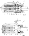
- FIG. 1 a section through a connector system 1 is shown.
- the connector system 1 has an electrical connector 2 and an electrical circuit 3, which is designed as a printed circuit board 3 in the exemplary embodiment.
- the connector 2 also has a longitudinal axis L, which runs along a plug-in direction, indicated in the figure by a double arrow.
- any electrical circuit can in principle be provided, for example in the form of a multi-chip module, a system-in-package, a system-on-chip and / or any integrated circuit, e.g. B. also a single microchip or ASIC.
- the invention is described in the exemplary embodiment using a printed circuit board 3, but this can be understood as a "black box" for any electrical circuit.
- the connector 2 has a housing 4, which in the present embodiment is made of a non-conductive material, for. B. is formed from a plastic.
- the housing 4 serves, among other things, to accommodate an electrical line 5, which in the exemplary embodiment is designed as a cable 5 that is held in the housing 4 of the plug connector 2 via a holding device 6.
- the cable 5 is an electrically shielded cable 5 with a ground conductor which is designed as an outer conductor 7, in particular as a braided shield 7, which is electrically conductively connected to a means for shielding 8 of the connector 2.
- the outer conductor 7 carries a defined electrical potential, in particular a ground potential, which is suitable for forming a shield.
- the braided shield 7 is clamped between the shielding means 8 and the housing 4 of the connector 2.
- the means for shielding 8 preferably extends completely around the inner regions of the connector 2 in order to shield the connector 2 completely electromagnetically.
- signal conductors 10 which in the exemplary embodiment are designed as inner cable conductors 10 of cable 5, are electrically connected at their ends facing circuit board 3 to contacts 9 on the input side.
- the connector 2 has contacts 11 on the output side, which are electrically connected to connector inner conductors 12.
- three contacts 9, 11 are provided in each case. The number can be arbitrary in the present case.
- the plug connector 2 has a receptacle 13 for the printed circuit board 3, which is designed as a slot-shaped recess 13 between the input-side contacts 9 and the output-side contacts 11.
- the receptacle 13 has an access opening 14 through which the circuit board 3 can be inserted.
- a closure element 15 is provided to close the access opening 14.
- the circuit board 3 has contact points 16, which in the present case are designed as flat contacts 16 or soldering areas which, in the case of the circuit board 3 used (as shown), make contact with the input-side contacts 9 and the output-side contacts 11.
- the circuit board 3 used is positioned between the input-side contacts 9 and the output-side contacts 11.
- the contacts 9, 11 of the plug connector 2 are designed as spring contacts 9, 11 in the present case.
- the circuit board 3 has conductor tracks, plated-through holes (not shown here) and electrical components 17 or electrical components. In this way, an individual transmission option from the input-side contacts 9 to the output-side contacts 11 can be guaranteed.
- the transmission options are diverse. Thus, for example, signal amplifications, impedance adjustments, linearizations up to an automatic adjustment with regard to the currently installed cable length and programmable circuits can be provided. It can also be provided that the printed circuit board 3 only has conductor tracks and / or plated-through holes, which enables a variable and quickly exchangeable assignment or rewiring of the plug connector 2.
- the housing 4 of the plug connector 2 optionally has a mechanical coding, by means of which the plug connector 2, which in the present case is designed as a plug, can be plugged into a socket (not shown), for example.
- the connector 2 can basically be a plug, a socket, a coupling or an adapter.
- the connector 2 can also be used as a printed circuit board connector or be accommodated in a device housing.
- the connector 2 can have contact sleeves 18 in its front area, which are electrically connected to the connector inner conductors 12.
- the closure element 15 is preferably formed essentially from plastic or from a non-conductive material and has an electrically conductive attachment 19 in the form of a contact spring attachment 19.
- the attachment 19 makes electrical contact with the shielding means 8 of the connector 2 and thus ensures a closed electromagnetic shielding.
- the closure element 15 comprises a seal 20 for mechanically sealing the access opening 14.
- a contact element 21 is also provided on the closure element 15, which, in the manner of an additional contact spring, electrically connects the electrically conductive attachment 19 of the closure element 15 to a circuit shield, in this case a circuit board shield 22 in the form of a metallized surface of the circuit board 3. Furthermore, a further contact element 23 of a similar design is provided at the lower end of the receptacle 13, which contact element also makes contact with the circuit board shielding 22 of the circuit board 3. In principle, electrical contacting of the shields 8, 19, 22 on all sides and over a large area is advantageous.
- one or all of the contact elements 21, 23 can also be provided on the circuit board 3 or on the circuit board shield 22.
- a printed circuit board shield 22 can also be implemented without necessarily providing electrical contact with the attachment 19 via the contact element.
- the circuit board 3 and in particular its sectional structure is shown only as an example and in a highly abstracted manner.
- the circuit board 3 can be a one-sided circuit board, a two-sided circuit board or a multilayer circuit board 3 with more than two circuit board layers.
- a circuit board 3 with two circuit board layers 26 is described later in FIG Figure 11 shown enlarged.
- the illustrated connector system 1 can advantageously be set up for the transmission of electrical signals according to a USB standard.
- FIG 2 is that in Figure 1 illustrated connector system 1 is shown again, wherein the circuit board 3 has been removed. Furthermore, the closure element 15 is not inserted into the access opening 14.
- the input-side contacts 9 and the output-side contacts 11 do not make electrical contact when the printed circuit board 3 is removed. This is a constructively preferable solution, since the implementation of such an arrangement is easy to handle. It can also be advantageous, by removing the printed circuit board 3, to effect a reliable galvanic separation of circuits within the plug connector 2. It can also be understood as in the context of the invention to provide a printed circuit board 3, which only ensures reliable galvanic separation between some or all of the contacts 9, 11.
- the printed circuit board 3 would accordingly have a transfer option or a transfer function of zero between at least one input-side contact 9 and at least one output-side contact 11.
- the circuit board 3 can thus also serve as a securing element - either in the inserted or removed state, depending on the design.
- the relaxed length of the springs when the contacts 9, 11 are designed as springs or the distances between the contacts 9, 11 are selected such that the input-side contacts 9 and the output-side contacts 11 themselves contact one another if the printed circuit board 3 is not inserted.
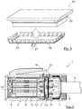
- FIG 3 is the closure element 15 of the Figures 1 and 2 enlarged and shown in a spatial representation.
- the closure element 15 is essentially formed from a non-conductive material and comprises the seal 20 already described.
- the conductive attachment 19 is preferably formed from a sheet metal and pushed or placed onto the closure element 15. Lateral contact springs 24 are provided, thereby ensuring reliable electrical contact with the outer conductor 7 of the cable 5 or with the means for shielding 8 of the connector 2 can be guaranteed even when large tolerances are to be compensated.
- the contact springs 24 are preferably arranged in a ring around the closure element 15. In a simplified design, however, a single contact or a single contact spring 24 can also be sufficient.
- closure element 15 is formed in a simplified embodiment as a sheet metal element or completely from metal.
- the closure element 15 is positively and non-positively connected to the means for shielding 8 of the plug connector 2 by, for example, a screw connection.
- the closure element 15 is preferably arranged set back in the inserted state in the housing 4 of the plug connector 2.
- a coplanar design or a design in which the closure element 15 protrudes from the housing 4 is also possible (see e.g. Figure 1 ), possible.
- FIG Figure 5 A third embodiment of a connector system 1 according to the invention is shown in FIG Figure 5 shown.
- the connector 2 is designed as a coupling.
- the contact sleeve or the contact sleeves 18 of the front area of the plug connector 2 is or are arranged in the embodiment in relation to the circuit board 3 in such a way that a corresponding plug is able to make direct contact with the output-side contact points 16 of the circuit board 3.
- the output-side contact 11 is formed by the corresponding plug, which can be viewed as a component of the present connector system 1.
- the corresponding plug makes contact with the at least one output-side contact 11 of the plug connector 2.
- the output-side contacts 11 and the plug connector inner conductors 12 would be formed in one piece with the contact sleeves 18.
- FIG. 6 to 8 Simplified circuit diagrams are shown to show three exemplary variants of the connector system 1 or to show examples of the various transmission options from the at least one input-side contact 9 to the at least one output-side contact 11.
- the input-side contact 9 of the connector 2 with the cable inner conductors 10 and the output-side contact 11 of the connector 2 with the connector inner conductors 12 and the printed circuit board 3 are shown in each case.
- the electrical contacting of the contacts 9, 11 of the connector 2 and the contact points 16 of the printed circuit board 3 are only shown very schematically.
- circuit board 3 functions only for the forwarding or direct contacting of the cable inner conductors 10 with the plug connector inner conductors 12.
- the circuit board 3 can only have vias for this purpose.
- the circuit board 3 and the transmission option then function as a so-called "dummy" element.
- Figure 7 is one of the Figure 6 A similar embodiment is shown, in which the printed circuit board 3 once again only serves to make contact between the cable inner conductors 10 and the connector inner conductors 12, without providing any further influencing of the signals. However, in this embodiment it is a "crossover" connection, ie a cross-connection of signals and thus one of the Figure 6 different connector assignment.
- the plug connection 2 can thus be functionally changed.
- Figure 8 shows a further embodiment in which an electronics 25 of the circuit board 3 - shown as a "black box” - electrically influences one or more or all of the signals when they are passed on from the input-side contacts 9 to the output-side contacts 11.
- the invention can also be used to avoid or replace a conventional fan-out area within a plug connector or to adapt an input-side interface 30 and an output-side interface 31 in an impedance-controlled manner.
- the so-called pitch i. H. a center-to-center distance of the contacts 9, 11 or contact points 16 can be modified.
- the cable inner conductors 10 are fanned out, d. H. the pitch is expanded in order to achieve the correct proportions for the connector.
- Such a fanning out can be clearly seen in FIGS. 1, 2, 4 and 5.
- the cable inner conductors 10 are usually fanned out so that their ends assume a position such that each end of a cable inner conductor 10 is assigned a corresponding end of a connector inner conductor 12 and the ends assigned to one another run coaxially to one another.
- any number of unbundling options for the input-side and output-side interfaces (“interfaces”) 30, 31 are possible.
- Any pin assignments or plug connector standards can be adapted with the electrical circuit or printed circuit board 3, with impedance control being possible at the same time by appropriate circuit components of the electrical circuit or printed circuit board 3. For example, it is possible to switch from a transmission type or "stranding" with a star quad to a parallel transmission type ("parallel pair").
- Figure 9 shows a further example of different interfaces 30, 31 on the input side and on the output side, each with a different pitch.
- the output-side interface 31 therefore has greater distances between the individual cores or connector inner conductors 12.
- a fan-out area which, however, causes faults in the transmission path.
- both interfaces 30, 31 can have the same impedance (e.g. 90 ohms differential).
- a circuit board 3 can be provided, it being possible to first make direct contact with the circuit board 3 from both sides with the respective interface dimensions.
- a suitable design of the microstrip lines and vias of the circuit board 3 can then compensate for the capacitive behavior of the transition from the respective inner conductors 10, 12 to the circuit board 3.
- a reflection-free pitch change is preferably provided.
- the receptacle 13 for the circuit board 3 is not shown for the sake of simplicity.
- the printed circuit board 3 can, however, be inserted into the plug connector 2 as described above.
- connector 2 is the Figure 9 shown as a printed circuit board connector. As shown, the connector 2 is not connected on the input side to a cable 5, but to a further printed circuit board 32. A plurality of electrical lines 5 or signal conductors 10 of the further printed circuit board 32 can be contacted with corresponding contact lines 33. Contact can also be made with a ground conductor of the further printed circuit board 32, if necessary, by means of at least one contact line 33.
- the contact lines 33 connect the signal conductors 10 to the contact points 16 of the printed circuit board 3 or to the contacts 9 on the input side.
- an electrical circuit By using an electrical circuit according to the invention, a transition between an input-side interface 30 and an output-side interface 31 that is optimally suitable for high-frequency technology can be provided, with differences between the interfaces 30, 31 that would have a negative effect on the signal transmission, such as, in particular, different line lengths , Center-to-center distances or relative positioning of the contacts, geometry or size the individual contacts and the type of material of the individual contacts, through which the correspondingly designed electrical circuit can be electrically balanced or adapted.
- Figure 11 shows a schematic sectional view of a circuit board 3 in an optional configuration as a circuit board 3, as this could be used for the present invention. It can also be a multilayer printed circuit board.
- the circuit board 3 according to Figure 11 comprises a full circumferential metallization 22 made of copper, which forms the circuit board shield 22, on its surfaces or side faces.
- the metallization 22 is cut out around the contact points 16 so as not to short-circuit the contact points 16 to the shield.
- circuit board layers 26 which are connected by means of contacts 27 and are spaced apart from one another, are arranged within the metallization 22.
- the circuit board layers 26 of the circuit board 3 are connected to the contact points 16 via plated-through holes 28.
- Electrical components 17 are preferably arranged in each case on the inwardly directed sides of the circuit board layers 26.
- the plated-through holes 28 and contacts 27 can also be formed in one piece.
- a thermally conductive layer 29 can be formed between the circuit board layers 26 and the electrical components 17 surrounding or immediately adjacent or adjoining.
- the distance between the circuit board layers 26 can depend, among other things, on the level and / or operating voltage of the electrical components 17 and on the electrical insulation capacity of the thermally conductive layer 29.
- the thermally conductive layer 29 can comprise epoxy resin. Due to the low thermal conductivity of epoxy resin, the thermally conductive layer 29 can also be enriched with boron nitride and / or aluminum oxide. Accordingly, the required thickness of the thermally conductive layer 29 can largely depend on its composition.
- epoxy resin instead of epoxy resin, synthetic resin can also be used accordingly. This is also particularly suitable.
- a connector 2 of the above-described embodiments of Figures 1, 2 and 4 to 10 also be designed in two parts.
Description
Die Erfindung betrifft ein Steckverbindersystem, aufweisend einen elektrischen Steckverbinder zur Verbindung mit wenigstens einer elektrischen Leitung sowie eine elektrische Schaltung.The invention relates to a connector system having an electrical connector for connection to at least one electrical line and an electrical circuit.
Steckverbinder zum Trennen und Verbinden von Leitungen sind hinlänglich bekannt und werden insbesondere in der Elektrotechnik in vielfältiger Form eingesetzt. Bei einem Steckverbinder kann es sich um einen Stecker, eine Buchse, eine Kupplung oder einen Adapter handeln. Insbesondere kann der Steckverbinder zur Verbindung mit wenigstens einem Kabel und/oder mit wenigstens einer Leiterplatte (auch "Printed Circuit Board", PCB genannt) verwendet werden. Die im Rahmen der Erfindung verwendete Bezeichnung "Steckverbinder" steht stellvertretend für alle Varianten.Plug connectors for separating and connecting lines are well known and are used in various forms, especially in electrical engineering. A connector can be a plug, a socket, a coupling or an adapter. In particular, the plug connector can be used to connect to at least one cable and / or to at least one printed circuit board (also called “printed circuit board”, PCB). The term "connector" used in the context of the invention is representative of all variants.
Unter anderem aufgrund der fortschreitenden Entwicklung in der Digitaltechnik werden signalverarbeitende Systeme, die teils über Kabelverbindungen und somit Steckverbinder miteinander verbunden werden müssen, zunehmend komplexer. Um eine ausreichend hohe Datenrate und Signalqualität der Kabelverbindung sicherzustellen, sind somit regelmäßig zusätzliche Schaltungskomponenten erforderlich.Due to the advancing development in digital technology, among other things, signal processing systems, some of which have to be connected to one another via cable connections and thus connectors, are becoming increasingly complex. In order to ensure a sufficiently high data rate and signal quality of the cable connection, additional circuit components are therefore regularly required.
Insbesondere zum Erreichen von hohen Datenraten kann es notwendig sein, die verbauten Kabellängen zu berücksichtigen und beispielsweise Impedanzen bzw. Wellenwiderstände anzugleichen und/oder die zu übertragenen Signale anwendungsspezifisch aufzubereiten, d. h. zu dämpfen, zu verstärken, zu linearisieren oder auf sonstige Weise zu manipulieren.In order to achieve high data rates in particular, it may be necessary to take the built-in cable lengths into account and, for example, to adjust impedances or wave resistances and / or to prepare the signals to be transmitted in an application-specific manner, i. H. to dampen, amplify, linearize or otherwise manipulate.
Schließlich ergibt sich eine große Vielfalt von Varianten bezüglich der erforderlichen Komponenten für die Signalaufbereitung, die von den Herstellern meist individuell bereitgestellt werden muss.Ultimately, there is a large variety of variants with regard to the components required for signal processing, which the manufacturers usually have to provide individually.
Es hat sich gezeigt, dass es ein fertigungstechnischer Vorteil sein kann, Schaltungskomponenten und mitunter ganze Leiterplatten in eine Kabelanordnung oder eine Steckverbindung zu integrieren. Derartige Steckverbinder sind beispielsweise aus der
In Abhängigkeit der Anwendung kann ein Kabelaustausch im Gegensatz zu einem Austausch anderer Systemkomponenten teilweise schnell und einfach erfolgen. Ein derartiger Austausch kann aus vielen Gründen, beispielsweise wegen Beschädigungen oder einer Systemänderung bzw. einer Systemerweiterung, erforderlich sein.Depending on the application, cables can be replaced quickly and easily, in contrast to other system components. Such an exchange can be necessary for many reasons, for example because of damage or a system change or system expansion.
Allerdings kann selbst ein Kabelaustausch in vielen Fällen nur schwer durchgeführt werden. Dies gilt insbesondere für die Automobil- oder die Luft- und Raumfahrtindustrie. Beispielsweise sind auf Grund von Bauraumbeschränkungen verlegte Kabel in einem Kraftfahrzeug meist nur in Teilbereichen, z. B. im Bereich von Steckverbindungen, ohne großen Demontageaufwand zugänglich.However, even a cable replacement can be difficult in many cases. This is especially true for the automotive or aerospace industries. For example, due to installation space restrictions, cables laid in a motor vehicle are usually only in partial areas, e.g. B. in the area of connectors, accessible without major disassembly effort.
Außerdem ist selbst die Herstellung von verschiedenen Kabelanordnungen in der zumeist notwendigen Vielfalt aufwändig und kostenintensiv.In addition, even the production of different cable arrangements in the mostly necessary variety is complex and cost-intensive.
Ein weiteres Problem der bekannten Steckverbinder besteht darin, dass ein Kabelinterface meist einer Auffächerung bedarf, um den geometrischen Erfordernissen des Steckverbinderinterface gerecht zu werden. Ein solcher Auffächerbereich ist allerdings insbesondere für die Übertragung von hochfrequenten Signalen kritisch und kann die Signalqualität negativ beeinträchtigen.Another problem with the known plug connectors is that a cable interface usually needs to be fanned out in order to meet the geometric requirements of the plug connector interface. However, such a fan-out area is particularly critical for the transmission of high-frequency signals and can negatively affect the signal quality.
Zum weiteren technischen Hintergrund wird auf die
In Anbetracht des bekannten Stands der Technik besteht die Aufgabe der vorliegenden Erfindung somit darin, ein verbessertes Steckverbindersystem bereitzustellen, bei dem eine Anpassung der Verschaltung noch leichter möglich ist, als mit dem derzeitigen Stand der Technik.In view of the known state of the art, the object of the present invention is to provide an improved connector system in which the interconnection can be adapted even more easily than with the current state of the art.
Diese Aufgabe wird für das Steckverbindersystem mit den in Anspruch 1 aufgeführten Merkmalen gelöst. Die abhängigen Ansprüche und die nachfolgend beschriebenen Merkmale betreffen vorteilhafte Ausführungsformen und Varianten der Erfindung.This object is achieved for the connector system with the features listed in
Das erfindungsgemäße Steckverbindersystem weist einen elektrischen Steckverbinder zur Verbindung mit wenigstens einer elektrischen Leitung sowie eine elektrische Schaltung auf.The connector system according to the invention has an electrical connector for connection to at least one electrical line and an electrical circuit.
Die elektrische Schaltung weist vorzugsweise zumindest ein elektrisches Bauteil auf.The electrical circuit preferably has at least one electrical component.
Unter einer elektrischen Leitung ist eine beliebige Einrichtung zum Transport bzw. zur Übertragung von elektrischer Energie zur Datenübertragung und/oder zur elektrischen Versorgung zu verstehen. Vorzugsweise handelt es sich bei der elektrischen Leitung um ein elektrisches Kabel bestehend aus einem Verbund mehrerer Einzelleitungen. Ein elektrisches Kabel weist dabei im Allgemeinen einen Masseleiter bzw. Außenleiter und einen oder mehrere Signalleiter in Form von Innenleitern auf.An electrical line is to be understood as any device for transporting or transmitting electrical energy for data transmission and / or for electrical supply. The electrical line is preferably an electrical cable consisting of a combination of several individual lines. An electrical cable generally has a ground conductor or outer conductor and one or more signal conductors in the form of inner conductors.
Es kann im Sinne der Erfindung aber auch vorgesehen sein, dass es sich bei der elektrischen Leitung um eine elektrische Leitung eines elektrischen Geräts, eines weiteren Steckverbinders oder einer elektrischen Leitung auf einer Leiterplatte, beispielsweise um eine Mikrostreifenleitung oder eine Verbindungsstelle zu einer Mikrostreifenleitung, handelt.In the context of the invention, however, it can also be provided that the electrical line is an electrical line of an electrical device, a further plug connector or an electrical line on a circuit board, for example a microstrip line or a connection point to a microstrip line.
Unter dem Begriff "Masseleiter" kann sinngemäß ein beliebiger elektrischer Leiter verstanden werden, der ein Massepotenzial oder ein sonstiges Bezugspotenzial führt.The term “ground conductor” can be understood to mean any electrical conductor that carries a ground potential or some other reference potential.
Unter dem Begriff "Signalleiter" kann sinngemäß ein beliebiger Leiter zur Übertragung von elektrischen Datensignalen und/oder elektrischen Versorgungssignalen verstanden werden.The term “signal conductor” can be understood to mean any conductor for the transmission of electrical data signals and / or electrical supply signals.
Zum besseren Verständnis wird die Erfindung nachfolgend im Wesentlichen anhand der Verbindung mit einem elektrischen Kabel beschrieben. Dies ist nicht einschränken zu verstehen. Der Fachmann vermag die Begriffe "Kabel", "Außenleiter" und "Innenleiter" ohne Weiteres auf die allgemeineren Begriffe "Leitung", "Masseleiter" und "Signalleiter" zu übertragen.For a better understanding, the invention is described below essentially on the basis of the connection with an electrical cable. This is not to be understood as limiting. The person skilled in the art can easily transfer the terms “cable”, “outer conductor” and “inner conductor” to the more general terms “line”, “ground conductor” and “signal conductor”.
Vorzugsweise kann der Steckverbinder ein Gehäuse zur Aufnahme der wenigstens einen elektrischen Leitung, beispielsweise zur Aufnahme eines elektrischen Kabels, aufweisen.The plug connector can preferably have a housing for receiving the at least one electrical line, for example for receiving an electrical cable.
In einer bevorzugten Ausführungsform kann insbesondere ein einzelnes Kabel von dem Gehäuse aufgenommen werden. Zur Aufnahme des wenigstens einen Kabels kann es von Vorteil sein, aus dem Stand der Technik hinlänglich bekannte Mittel zur Abdichtung und/oder zum Zugabfang von Kräften, die an dem Kabel wirken, vorzusehen.In a preferred embodiment, in particular, a single cable can be received by the housing. To accommodate the at least one cable, it can be advantageous to provide means for sealing and / or for intercepting forces that act on the cable, which are well known from the prior art.
Bei dem Gehäuse kann es sich um ein elektrisch leitfähiges Gehäuse, beispielsweise bestehend aus einem Metall, oder bevorzugt, um ein elektrisch nicht leitendes Gehäuse, beispielsweise bestehend aus einem Kunststoff, handeln. Auch eine Mischform ist möglich. Die Verwendung eines Kunststoffgehäuses ist zumeist fertigungstechnisch einfacher und kann aufgrund der isolierenden Eigenschaften, je nach Einsatzort, auch aus elektrotechnischer Sicht Vorteile bieten.The housing can be an electrically conductive housing, for example consisting of a metal, or preferably an electrically non-conductive housing, for example consisting of a plastic. A mixed form is also possible. The use of a plastic housing is usually simpler in terms of production technology and, depending on the place of use, can also offer advantages from an electrical engineering point of view due to the insulating properties.
Der elektrische Steckverbinder umfasst erfindungsgemäß ferner wenigstens einen eingangsseitigen Kontakt, der mit einem Signalleiter der elektrischen Leitung (z. B. einem Kabel-Innenleiter eines elektrischen Kabels) verbindbar ist, und wenigstens einen ausgangsseitigen Kontakt, der mit einem Steckverbinder-Innenleiter elektrisch verbindbar ist.According to the invention, the electrical connector further comprises at least one input-side contact that can be connected to a signal conductor of the electrical line (e.g. a cable inner conductor of an electrical cable), and at least one output-side contact that can be electrically connected to a connector inner conductor.
Der eingangsseitige Kontakt des Steckverbinders, mit dem der elektrische Leiter verbunden ist bzw. an dem das wenigstens eine Kabel mit dem wenigstens einen Innenleiter aufgenommen wird und der ausgangsseitige Kontakt des Steckverbinders sind somit grundsätzlich, das heißt ohne weitere, nachfolgend beschriebene Maßnahmen und Ausgestaltungen, nicht miteinander elektrisch verbunden.The input-side contact of the connector to which the electrical conductor is connected or at which the at least one cable with the at least one inner conductor is received and the output-side contact of the connector are therefore fundamentally, i.e. without further measures and configurations described below, not electrically connected to each other.
In einer besonders bevorzugten Ausführung sind der wenigstens eine eingangsseitige Kontakt und der wenigstens eine ausgangsseitige Kontakt räumlich voneinander separiert. Die beiden Kontakte können gegenüberliegend, d. h. in einer Linie bzw. Achse angeordnet sein. Vorzugsweise sind die aufeinander zugewandten Enden der eingangsseitigen Kontakte und der ausgangsseitigen Kontakte in zwei einander gegenüberliegenden, vorzugsweise parallel zueinander verlaufenden Ebenen angeordnet.In a particularly preferred embodiment, the at least one input-side contact and the at least one output-side contact are spatially separated from one another. The two contacts can be opposite, i. H. be arranged in a line or axis. Preferably, the mutually facing ends of the input-side contacts and the output-side contacts are arranged in two mutually opposite, preferably parallel, planes.
Es kann vorgesehen sein, dass ein einpoliger Steckverbinder oder ein mehrpoliger Steckverbinder verwendet wird. Das heißt, es kann vorgesehen sein, jeweils einen eingangsseitigen Kontakt und einen ausgangsseitigen Kontakt oder mehr als einen eingangsseitigen Kontakt und mehr als einen ausgangsseitigen Kontakt vorzusehen. Vorzugsweise sind jeweils zwei bis zwanzig eingangsseitige Kontakte, besonders bevorzugt drei bis zehn eingangsseitige Kontakte und ganz besonders bevorzugt bis zu vier eingangsseitige Kontakte vorgesehen. Die Anzahl der ausgangsseitigen Kontakte ist vorzugsweise analog gestaltet.It can be provided that a single-pole connector or a multi-pole connector is used. That is to say, provision can be made to provide one input-side contact and one output-side contact or more than one input-side contact and more than one output-side contact. Preferably, two to twenty input-side contacts, particularly preferably three to ten input-side contacts and very particularly preferably up to four input-side contacts, are provided in each case. The number of contacts on the output side is preferably designed analogously.
Es kann auch vorgesehen sein, dass sich die Anzahl eingangsseitiger Kontakte und ausgangsseitiger Kontakte voneinander unterscheidet.It can also be provided that the number of input-side contacts and output-side contacts differ from one another.
Ferner können sich auch die Anzahl Signalleiter bzw. Kabel-Innenleiter und eingangsseitige Kontakte bzw. die Anzahl Steckverbinder-Innenleiter und ausgangsseitige Kontakte unterscheiden. Es können z. B. mehrere Signalleiter bzw. Kabel-Innenleiter auf denselben eingangsseitigen Kontakt zusammengeführt werden.Furthermore, the number of signal conductors or cable inner conductors and input-side contacts or the number of plug-in connector inner conductors and output-side contacts can also differ. It can e.g. B. several signal conductors or cable inner conductors are brought together on the same input-side contact.
Erfindungsgemäß weist der elektrische Steckverbinder ferner Mittel zur Abschirmung auf, die mit einem Masseleiter der wenigstens einen elektrischen Leitung (z. B. einem Außenleiter des wenigstens einen Kabels) elektrisch verbindbar sind.According to the invention, the electrical connector also has means for shielding, which can be electrically connected to a ground conductor of the at least one electrical line (for example an outer conductor of the at least one cable).
Insbesondere zum Erreichen hoher Datenraten ist eine Abschirmung gegen ungewollte elektrische bzw. elektromagnetische Einflüsse erforderlich. Es hat sich gezeigt, dass es von Vorteil ist, wenn nicht nur die Signalleitung bzw. das Kabel selbst, sondern auch die Steckverbindung sowie die elektrischen Komponenten der Steckverbindung eine hohe elektromagnetische Verträglichkeit (EMV) und somit geeignete Mittel zur Abschirmung aufweisen.Shielding against undesired electrical or electromagnetic influences is necessary, in particular to achieve high data rates. It has been shown that it is advantageous if not only the signal line or the cable itself, but also the plug connection and the electrical components of the plug connection have high electromagnetic compatibility (EMC) and thus suitable means for shielding.
Erfindungsgemäß ist ferner vorgesehen, dass der Steckverbinder eine Aufnahme für die elektrische Schaltung und ein Verschlusselement zum Verschließen einer Zugangsöffnung der Aufnahme aufweist.According to the invention it is further provided that the plug connector has a receptacle for the electrical circuit and a closure element for closing an access opening of the receptacle.
Die Aufnahme ist dabei vorzugsweise derart angeordnet, dass diese den wenigstens einen eingangsseitigen Kontakt und den wenigstens einen ausgangsseitigen Kontakt räumlich voneinander trennt bzw. sich zwischen dem wenigstens einen eingangsseitigen Kontakt und dem wenigstens einen ausgangsseitigen Kontakt befindet.The receptacle is preferably arranged in such a way that it spatially separates or separates the at least one input-side contact and the at least one output-side contact is located between the at least one input-side contact and the at least one output-side contact.
Die elektrische Schaltung weist Kontaktstellen auf, um wenigstens einen eingangsseitigen Kontakt und wenigstens einen ausgangsseitigen Kontakt zu kontaktieren, wenn die elektrische Schaltung in die Aufnahme eingesetzt ist. Ferner weist die elektrische Schaltung eine Übertragungsmöglichkeit von dem wenigstens einen eingangsseitigen Kontakt zu dem wenigstens einen ausgangsseitigen Kontakt auf. Die Übertragungsmöglichkeiten können bei einer Mehrzahl elektrischer Leitungen oder bei einer Mehrzahl Signalleiter individuell für jede Leitung bzw. für jeden Signalleiter bzw. für jeden Kontakt bzw. für jedes zu übertragende Signal ausgelegt sein.The electrical circuit has contact points in order to contact at least one input-side contact and at least one output-side contact when the electrical circuit is inserted into the receptacle. Furthermore, the electrical circuit has a transmission option from the at least one input-side contact to the at least one output-side contact. With a plurality of electrical lines or with a plurality of signal conductors, the transmission options can be designed individually for each line or for each signal conductor or for each contact or for each signal to be transmitted.
In einer besonders bevorzugten Ausführungsform kann die elektrische Schaltung derart zwischen den wenigstens einen eingangsseitigen Kontakt und den wenigstens einen ausgangsseitigen Kontakt eingeschoben werden, dass eine Kontaktstelle bzw. Kontaktstellen einer eingangsseitigen Kontaktfläche der elektrischen Schaltung den wenigstens einen eingangsseitigen Kontakt kontaktieren und eine Kontaktstelle bzw. Kontaktstellen einer ausgangsseitigen Kontaktfläche der elektrischen Schaltung (die vorzugsweise parallel zu der eingangsseitigen Kontaktfläche verläuft und entgegengesetzt ausgerichtet ist) den wenigstens einen ausgangsseitigen Kontakt kontaktieren.In a particularly preferred embodiment, the electrical circuit can be inserted between the at least one input-side contact and the at least one output-side contact that a contact point or contact points of an input-side contact surface of the electrical circuit contact the at least one input-side contact and a contact point or contact points of a contact surface of the electrical circuit on the output side (which preferably runs parallel to the contact surface on the input side and is oriented in the opposite direction) contact the at least one contact on the output side.
In einer Weiterbildung der Erfindung kann insbesondere vorgesehen sein, dass die elektrische Schaltung als Leiterplatte, vorzugsweise als zweiseitige Leiterplatte (mit zwei Leiterplattenlagen) oder als Multilagenleiterplatte mit mehr als zwei Leiterplattenlagen, als Multi-Chip-Modul, als System-in-Package, als System-on-Chip und/oder als integrierte Schaltung ausgebildet ist.In a further development of the invention, it can be provided in particular that the electrical circuit as a circuit board, preferably as a two-sided circuit board (with two circuit board layers) or as a multi-layer circuit board with more than two circuit board layers, as a multi-chip module, as a system-in-package, as System-on-chip and / or is designed as an integrated circuit.
Die elektrische Schaltung kann in einer besonders bevorzugten Variante als Leiterplatte mit einer oder mehreren Leiterplattenlagen ausgebildet sein, wobei die Leiterplatte beispielsweise Leiterbahnen, Durchkontaktierungen ("Vias") und/oder elektrische Bauelemente, wie z. B. Widerstände, Kapazitäten, Induktivitäten und/oder Halbleiterschaltungen bis hin zu komplexen integrierten Schaltungen bzw. Mikrochips bzw. anwendungsspezifischen integrierten Schaltungen ("Application Specific Integrated Circuits", ASICs), aufweisen kann.In a particularly preferred variant, the electrical circuit can be designed as a printed circuit board with one or more printed circuit board layers. B. resistors, capacitances, inductances and / or semiconductor circuits up to complex integrated circuits or microchips or application-specific integrated circuits ("Application Specific Integrated Circuits", ASICs).
Unter einer Leiterplatte mit mehreren Lagen, also z. B. auch unter einer "Multilagenleiterplatte", kann vorliegend auch ein System aus mehreren (bestückten oder unbestückten) einseitigen oder zweiseitigen Leiterplatten verstanden werden.Under a printed circuit board with several layers, so z. B. also under a "multilayer printed circuit board", a system of several (fitted or unpopulated) one-sided or two-sided printed circuit boards can also be understood in the present case.
Es kann zur Ausbildung der elektrischen Schaltung auch vorgesehen sein, mehrere Mikrochips in der Art eines sogenannten "Multi-Chip-Moduls" übereinander und/oder nebeneinander in einem gemeinsamen Chip-Gehäuse ("Package") anzuordnen, wobei die Mikrochips innerhalb des Chip-Gehäuses untereinander und/oder mit den Kontaktstellen des Chip-Gehäuses bzw. der elektrischen Schaltung über sogenannte Bonddrähte - oder durch eine sonstige bekannte Verbindungstechnik - verbunden sind.It can also be provided for the formation of the electrical circuit to arrange several microchips in the manner of a so-called "multi-chip module" one above the other and / or next to one another in a common chip housing ("package"), the microchips within the chip Housing among each other and / or are connected to the contact points of the chip housing or the electrical circuit via so-called bond wires - or by some other known connection technology.
Schließlich kann die elektrische Schaltung auch als "System-in-Package" ausgebildet sein, wobei einer oder mehrere Mikrochips zusammen mit wenigstens einem weiteren elektrischen Bauteil (z. B. zusammen mit Koppelkondensatoren) innerhalb eines gemeinsamen Chip-Gehäuses angeordnet und durch Bonddrähte (oder auf sonstige Weise) miteinander und/oder mit den Kontaktstellen der elektrischen Schaltung verbunden sind.Finally, the electrical circuit can also be designed as a "system-in-package", wherein one or more microchips are arranged together with at least one further electrical component (e.g. together with coupling capacitors) within a common chip housing and are connected by bonding wires (or in any other way) are connected to one another and / or to the contact points of the electrical circuit.
Es kann auch ein sogenanntes "System-on-Chip" oder ein herkömmlicher Mikrochip bzw. eine einzelne anwendungsspezifische integrierte Schaltung in einem Chip-Gehäuse mit an dem Chip-Gehäuse angeordneten Kontaktstellen vorgesehen sein, um die elektrische Schaltung zu realisieren.A so-called "system-on-chip" or a conventional microchip or a single application-specific integrated circuit can also be provided in a chip housing with contact points arranged on the chip housing in order to implement the electrical circuit.
Zur Vereinfachung wird die Erfindung nachfolgend im Wesentlichen durch Verwenden einer Leiterplatte als elektrische Schaltung beschrieben. Dies ist aber nicht einschränkend zu verstehen.For the sake of simplicity, the invention is described below essentially by using a printed circuit board as the electrical circuit. However, this is not to be understood as restrictive.
Vorzugsweise kann die elektrische Schaltung, insbesondere eine Multilagenleiterplatte, eine Metallisierung an wenigstens einer Oberfläche, vorzugsweise an allen nach außen gewandten Oberflächen aufweisen.The electrical circuit, in particular a multilayer printed circuit board, can preferably have a metallization on at least one surface, preferably on all surfaces facing outwards.
Das erfindungsgemäße Steckverbindersystem ermöglicht die Verwendung eines modularen Steckverbinders, welcher durch Einschub einer bestimmten elektrischen Schaltung, z. B. einer Leiterplatte mit einer gewünschten Elektronik, beispielsweise signalverbessernde Eigenschaften zeigt. Die Funktionen des Steckverbinders können somit durch verschiedenartige elektrische Schaltungen definiert werden. Dabei können der Steckverbinder und die mit dem Steckverbinder verbundene elektrische Leitung für eine Vielzahl von Anwendungen in identischer Weise hergestellt werden. Lediglich die elektrischen Schaltungen müssen individuell an die spezifische Anwendungsvariante angepasst werden. Ferner ist der Einbau bzw. die Montage der elektrischen Schaltung einfach möglich. Somit könnte sogar ein Endabnehmer über die zu verbauende Variante entscheiden oder in einfacher Weise eine Änderung der Variante, beispielsweise eine Funktionserweiterung, vornehmen.The connector system according to the invention enables the use of a modular connector which, by inserting a specific electrical circuit, eg. B. a circuit board with a desired electronics, for example, shows signal-improving properties. The functions of the connector can thus be defined by various types of electrical circuits. The connector and the electrical line connected to the connector can be produced in an identical manner for a large number of applications. Only the electrical circuits have to be individually adapted to the specific application variant. Furthermore, the installation or assembly of the electrical circuit is easily possible. In this way, an end user could even decide on the variant to be installed or simply change the variant, for example an expansion of functions.
Der Nachteil, dass eine bereits verbaute Lösung nur für einen festgelegten Zweck verwendbar ist, wird durch die vorliegende Erfindung gelöst. Nahezu jegliche Art von Elektronik und somit Funktionalität kann beispielsweise in der Form einer Leiterplatte auch nachträglich verbaut werden.The disadvantage that an already installed solution can only be used for a specified purpose is solved by the present invention. Almost any type of electronics and thus functionality can also be retrofitted, for example in the form of a printed circuit board.
Für die meisten Anwendungen dürfte es von Vorteil sein, wenn die elektrische Schaltung, die in die Aufnahme einsetzbar ist, nur einmalig vom Hersteller eingesetzt und dadurch die Funktionalität des Steckverbinders bzw. des mit diesem verbundenen Kabels festgelegt wird.For most applications, it should be advantageous if the electrical circuit that can be inserted into the receptacle is only used once by the manufacturer, thereby defining the functionality of the connector or the cable connected to it.
Das beschriebene Steckverbindersystem kann insbesondere im Automobilbereich vorteilhaft eingesetzt werden. Dabei können Komponenten schnell und kostengünstig modifiziert werden, ohne dass ein Eingriff in die angrenzende Elektronik notwendig ist oder ein Austausch eines gesamten Kabels, einer Platine und/oder eines Geräts, z. B. eines Steuergeräts, erforderlich wäre.The connector system described can be used particularly advantageously in the automotive sector. Components can be modified quickly and inexpensively without having to intervene in the adjacent electronics or replacing an entire cable, circuit board and / or device, e.g. B. a control unit would be required.
Das erfindungsgemäße Steckverbindersystem kann auch in der Art eines Adapters bzw. Adaptersteckers verwendet werden.The connector system according to the invention can also be used in the manner of an adapter or adapter plug.
Es kann auch vorgesehen sein, dass die elektrische Schaltung als Freischaltmodul für erweiterte Funktionen, die beispielsweise von einem Endabnehmer käuflich erworben werden können, einsetzbar ist. Das Steckverbindersystem kann somit zur Ausbildung eines Zugangsberechtigungssystems verwendbar sein.It can also be provided that the electrical circuit can be used as an activation module for extended functions that can be purchased, for example, by an end user. The connector system can thus be used to form an access authorization system.
In einer Weiterbildung der Erfindung kann vorgesehen sein, dass die elektrische Schaltung, wenn diese in die Aufnahme eingesetzt ist, zwischen dem wenigstens einen eingangsseitigen Kontakt und dem wenigstens einen ausgangsseitigen Kontakt positioniert ist. Die Kontakte und/oder Kontaktstellen können dabei (jeweils) alle mit derselben Kontaktart oder mit verschiedenen Kontaktarten realisiert sein. Es sind beliebige Kombinationen möglich.In a development of the invention it can be provided that the electrical circuit, when it is inserted into the receptacle, is positioned between the at least one input-side contact and the at least one output-side contact. The contacts and / or contact points can (each) all be implemented with the same type of contact or with different types of contact. Any combination is possible.
In einer Weiterbildung kann außerdem vorgesehen sein, dass die Kontaktstellen der elektrischen Schaltung und/oder die Kontakte des Steckverbinders als Flachkontakte und/oder Schleifkontakte und/oder Lötflächen (auch "Pads" genannt) und/oder Federkontakte (z. B. Pogo-Pins) und/oder Steckkontakte (männlich oder weiblich) ausgebildet sind.In a further development, it can also be provided that the contact points of the electrical circuit and / or the contacts of the connector are flat contacts and / or sliding contacts and / or soldering surfaces (also called "pads") and / or spring contacts (e.g. pogo pins ) and / or plug contacts (male or female) are formed.
Insbesondere wenn die elektrische Schaltung in die Aufnahme eingeschoben werden soll, haben sich die genannten Ausführungen der Kontaktstellen als vorteilhaft herausgestellt. Selbstverständlich sind auch weitere Kontaktierungsmöglichkeiten möglich, beispielsweise Ausführungen mit Kontaktschwertern und entsprechenden Aufnahmen für die Kontaktschwerter, und dergleichen.In particular, when the electrical circuit is to be pushed into the receptacle, the aforementioned designs of the contact points have proven to be advantageous. Of course, other contacting options are also possible, for example designs with contact blades and corresponding receptacles for the contact blades, and the like.
In einer Weiterbildung kann ferner vorgesehen sein, dass bei Ausbildung von Kontakten des Steckverbinders als Federkontakte die entspannte Länge der Federn und/oder die Abstände zwischen den Kontakten derart gewählt ist bzw. sind, dass wenigstens ein eingangsseitiger Kontakt und wenigstens ein ausgangsseitiger Kontakt auch dann kontaktieren, wenn die elektrische Schaltung nicht in die Aufnahme eingesetzt ist.In a further development, it can also be provided that when contacts of the connector are designed as spring contacts, the relaxed length of the springs and / or the distances between the contacts is or are selected such that at least one input-side contact and at least one output-side contact then also make contact when the electrical circuit is not inserted into the receptacle.
Für diesen Fall bietet es sich an, das aus einem eingangsseitigen Kontakt und einem ausgangsseitigen Kontakt zusammengesetzte Kontaktpaar in einer Linie gegenüberliegend anzuordnen.In this case, it is advisable to arrange the contact pair composed of an input-side contact and an output-side contact in a line opposite one another.
Es kann vorgesehen sein, dass selbst in dem Fall, in dem die elektrische Schaltung nicht in die Aufnahme eingesetzt ist, der wenigstens eine eingangsseitige Kontakt und der wenigstens eine ausgangsseitige Kontakt kontaktieren. Das Steckverbindersystem wäre somit selbst in diesem Zustand zumindest als Basisausführung verwendbar.It can be provided that even in the event that the electrical circuit is not inserted into the receptacle, the at least one input-side contact and the at least one output-side Contact contact. The connector system could therefore at least be used as a basic version even in this state.
Es kann auch vorgesehen sein, dass ohne eine eingesetzte elektrische Schaltung kein Kontakt besteht. Dies kann, auch bei einem Ausbilden der Kontakte als Federkontakte, beispielsweise durch eine versetzte, das heißt nicht auf einer Linie liegende Anordnung der Kontakte eines Kontaktpaars, realisiert werden.It can also be provided that there is no contact without an inserted electrical circuit. This can be implemented, even if the contacts are designed as spring contacts, for example by an offset arrangement of the contacts of a contact pair, that is to say not lying on a line.
Es kann vorgesehen sein, dass bei Verwendung eines mehrpoligen Steckverbinders einige Kontakte bereits bei einer nicht eingesetzten elektrischen Schaltung kontaktieren und andere Kontakte hingegen ausschließlich in einem eingesetzten Zustand der elektrischen Schaltung kontaktieren.It can be provided that, when using a multi-pole plug connector, some contacts already make contact when the electrical circuit is not in use and, on the other hand, make contact with other contacts only when the electrical circuit is in an inserted state.
Anwendungsspezifisch kann es erforderlich sein, zusätzliche elektrische Komponenten, beispielsweise zur Signalaufbereitung, über die elektrische Schaltung in das Steckverbindersystem zu integrieren.Depending on the application, it may be necessary to integrate additional electrical components, for example for signal processing, into the connector system via the electrical circuit.
Beispielsweise kann die Übertragungstechnik an den Übertragungskanal optimal anpassbar sein. Die Signalintegrität kann dann z. B. auf langen Leitungen erhalten bleiben, wobei insbesondere eine Anpassung der elektrischen Schaltung an die Kanallänge und/oder den Kanaltyp, beispielsweise die Kabellänge und den Kabeltyp, vorgesehen sein kann.For example, the transmission technology can be optimally adapted to the transmission channel. The signal integrity can then e.g. B. be retained on long lines, in particular an adaptation of the electrical circuit to the channel length and / or the channel type, for example the cable length and the cable type, can be provided.
Alternativ oder zusätzlich kann die elektrische Schaltung auch eine Umverdrahtung des Steckverbinders ermöglichen.As an alternative or in addition, the electrical circuit can also enable the connector to be rewired.
Erfindungsgemäß ist vorgesehen, dass das Verschlusselement zumindest teilweise aus einem elektrisch leitfähigen Material ausgebildet ist und das Verschlusselement, wenn dieses die Zugangsöffnung der Aufnahme verschließt, die Mittel zur Abschirmung des Steckverbinders elektrisch kontaktiert.According to the invention it is provided that the closure element is at least partially formed from an electrically conductive material and the closure element, when it closes the access opening of the receptacle, makes electrical contact with the means for shielding the connector.
Eine direkte oder indirekte elektrische Verbindung des Verschlusselements mit den Mitteln zur Abschirmung des Steckverbinders bzw. mit dem Masseleiter der wenigstens einen elektrischen Leitung bzw. mit dem Außenleiter des wenigstens einen Kabels kann in vorteilhafter Weise die Abschirmung des Steckverbinders und der elektrischen Schaltung, z. B. einer Leiterplatte sowie gegebenenfalls weiterer Komponenten innerhalb des Steckverbinders verbessern. Die elektromagnetische Verträglichkeit des Steckverbindersystems kann somit erhöht sein. Dabei kann eine möglichst großflächige bzw. vollständige und somit auch niederohmige Kontaktierung von Vorteil sein.A direct or indirect electrical connection of the closure element with the means for shielding the connector or with the ground conductor of the at least one electrical line or with the outer conductor of the at least one cable can advantageously shield the connector and the electrical circuit, e.g. B. improve a circuit board and possibly other components within the connector. The electromagnetic compatibility of the connector system can thus be increased. Contacting that is as large as possible or as complete as possible, and thus also with low resistance, can be advantageous.
Es kann vorgesehen sein, dass das Verschlusselement wenigstens eine Kontaktfeder aufweist, welche die Mittel zur Abschirmung des Steckverbinders elektrisch kontaktiert, wenn das Verschlusselement die Zugangsöffnung der Aufnahme verschließt.It can be provided that the closure element has at least one contact spring which electrically contacts the means for shielding the plug connector when the closure element closes the access opening of the receptacle.
Die Verwendung einer Kontaktfeder hat sich als besonders sichere elektrische Verbindung herausgestellt. Unabhängig von Oberflächenrauheiten, Fertigungstoleranzen und mechanischer sowie thermischer Beanspruchung des Steckverbindersystems während des Betriebs kann hierdurch eine definierte Kontaktmöglichkeit gewährleistet sein. Durch die Verwendung der Kontaktfeder kann ein großer Toleranzbereich ausgeglichen werden und ein "Loch" in der Abschirmung des Steckverbindersystems zu jeder Zeit vermieden werden.The use of a contact spring has proven to be a particularly safe electrical connection. Independent of surface roughness, manufacturing tolerances and mechanical and thermal stress on the connector system during operation, a defined contact option can be guaranteed. By using the contact spring, a large tolerance range can be compensated and a "hole" in the shielding of the connector system can be avoided at all times.
Es kann insbesondere vorgesehen sein, dass das Verschlusselement aus Kunststoff mit einem elektrisch leitfähigen Aufsatz oder (vorzugsweise vollständig) aus Metall ausgebildet ist.In particular, it can be provided that the closure element is made of plastic with an electrically conductive attachment or (preferably completely) made of metal.
Unter einem leitfähigen Aufsatz ist insbesondere ein Blech bzw. eine Konstruktion zu verstehen, die an der der Innenseite des Steckverbinders zugewandten Seite des Verschlusselements angebracht, beispielsweise verclipst oder verklebt, werden kann. Der leitfähige Aufsatz kann dabei vorzugsweise einteilig mit einer Kontaktfeder ausgebildet sein. Es kann auch vorgesehen sein, dass eine Kontaktfeder elektrisch leitfähig mit dem leitfähigen Aufsatz oder mit dem Metall des Verschlusselements verbunden ist. Die Kontaktfeder kann vorzugsweise eine elektrisch leitfähige Verbindung zwischen dem Mittel zur Abschirmung des Steckverbinders und dem Verschlusselement bzw. dem Aufsatz herstellen, wenn das Verschlusselement in die Zugangsöffnung eingesetzt ist.A conductive attachment is to be understood as meaning, in particular, a sheet metal or a construction which can be attached, for example clipped or glued, to the side of the closure element facing the inside of the connector. The conductive attachment can preferably be formed in one piece with a contact spring. It can also be provided that a contact spring is connected in an electrically conductive manner to the conductive attachment or to the metal of the closure element. The contact spring can preferably establish an electrically conductive connection between the means for shielding the plug connector and the closure element or the attachment when the closure element is inserted into the access opening.
In einer Weiterbildung der Erfindung kann vorgesehen sein, dass das Verschlusselement eine Dichtung zum Abdichten der Zugangsöffnung aufweist.In a development of the invention it can be provided that the closure element has a seal for sealing the access opening.
Mit einer Dichtung ist insbesondere eine mechanische Dichtung gegen Verschmutzung und/oder zum Schutz vor dem Eindringen von Flüssigkeiten gemeint. Dabei kann es sich um ein gummiartiges oder schaumstoffartiges Material oder dergleichen handeln.A seal means, in particular, a mechanical seal against contamination and / or for protection against the ingress of liquids. This can be a rubber-like or foam-like material or the like.
In einer Weiterbildung kann auch vorgesehen sein, dass das Verschlusselement in dem Gehäuse des Steckverbinders und/oder in dem Mittel zur Abschirmung des Steckverbinders und/oder in der Aufnahme kraftschlüssig und/oder stoffschlüssig und/oder formschlüssig fixierbar ist, vorzugsweise verklemmbar und/oder verschraubbar und/oder verklebbar und/oder verlötbar ist.In a further development, it can also be provided that the closure element can be fixed in the housing of the plug connector and / or in the means for shielding the plug connector and / or in the receptacle in a non-positive and / or cohesive and / or form-fitting manner, preferably clamped and / or screwed and / or can be glued and / or soldered.
Je nach Anwendung, Komplexität und Platzbedarf kann die Verwendung eines einfachen Verschlusselements, beispielsweise in Form eines Blechs, von Vorteil sein.Depending on the application, complexity and space requirement, the use of a simple closure element, for example in the form of a sheet metal, can be advantageous.
Es kann auch vorgesehen sein, dass die elektrische Schaltung, insbesondere eine Leiterplatte, mit dem Verschlusselement einteilig ausgebildet ist. Es kann somit vorgesehen sein, dass nach dem Einsetzen der elektrischen Schaltung bzw. Leiterplatte die elektrische Schaltung bzw. die Leiterplatte selbst die Zugangsöffnung der Aufnahme verschließt.It can also be provided that the electrical circuit, in particular a printed circuit board, is designed in one piece with the closure element. It can thus be provided that after the insertion of the electrical circuit or printed circuit board, the electrical circuit or the printed circuit board itself closes the access opening of the receptacle.
Weiter kann vorgesehen sein, dass die elektrische Schaltung eine Schaltungsabschirmung aufweist, und dass an dem Mittel zur Abschirmung des Steckverbinders und/oder an dem Masseleiter der wenigstens einen elektrischen Leitung und/oder an dem Verschlusselement und/oder an der elektrischen Schaltung wenigstens ein Kontaktelement vorgesehen ist bzw. sind, um die Schaltungsabschirmung mit dem Masseleiter der wenigstens einen elektrischen Leitung elektrisch zu kontaktieren, wenn die elektrische Schaltung in die Aufnahme eingesetzt ist.It can further be provided that the electrical circuit has a circuit shield and that at least one contact element is provided on the means for shielding the connector and / or on the ground conductor of the at least one electrical line and / or on the closure element and / or on the electrical circuit is or are to electrically contact the circuit shield with the ground conductor of the at least one electrical line when the electrical circuit is inserted into the receptacle.
Gegebenenfalls kann auch vorgesehen sein, die Schaltungsabschirmung mit wenigstens einem Signalleiter der wenigstens einen elektrischen Leitung elektrisch zu verbinden, insbesondere wenn ein Signalleiter ein definiertes Potential, beispielsweise ein Massepotential, führt, das geeignet ist, eine ausreichend gute Abschirmung auszubilden.If necessary, it can also be provided to electrically connect the circuit shield to at least one signal conductor of the at least one electrical line, in particular if a signal conductor carries a defined potential, for example a ground potential, which is suitable for forming a sufficiently good shield.
Eine separate Abschirmung der elektrischen Schaltung, z. B. eine Abschirmung der Leiterplatte zusätzlich zu der Abschirmung durch die Mittel zur Abschirmung des Steckverbinders, kann von Vorteil sein, um eine noch bessere elektromagnetische Verträglichkeit des Steckverbindersystems zu erzielen. Selbst wenn eine elektromagnetische Undichtigkeit des Steckverbinders, der die elektrische Schaltung umgibt, bestehen sollte, beispielsweise aufgrund von Beschädigungen, so wäre dennoch die empfindliche Elektronik, z. B. die Elektronik einer Leiterplatte, abgeschirmt.A separate shielding of the electrical circuit, e.g. B. a shielding of the circuit board in addition to the shielding by the means for shielding the connector, can be advantageous in order to achieve an even better electromagnetic compatibility of the connector system. Even if an electromagnetic leak in the connector that surrounds the electrical circuit should exist, for example due to damage, the sensitive electronics, e.g. B. the electronics of a circuit board, shielded.
Grundsätzlich ist es zu bevorzugen, das Steckverbindersystem redundant durch die Mittel zur Abschirmung (ggf. inklusive der Abschirmung durch das Verschlusselement) und die Kontaktierung der Schaltungsabschirmung gegen elektromagnetische Störungen abzusichern.In principle, it is preferable to redundantly secure the connector system against electromagnetic interference by means of the shielding means (possibly including the shielding by the closure element) and the contacting of the circuit shielding.
Wenn die elektrische Schaltung als mehrlagige Leiterlatte bzw. als Multilagenleiterplatte ausgebildet ist, kann die mehrlagige leiterplatte bzw. die Multilagenleiterplatte beispielsweise eine umlaufende Oberflächen- und Kantenmetallisierung aus Metall, vorzugsweise Kupfer zur Ausbildung der Schaltungsabschirmung aufweisen. Die umlaufende Metallisierung stellt eine besonders einfache und effektive Möglichkeit dar, die mehrlagige Leiterplatte bzw. die Multilagenleiterplatte vor elektromagnetischer Strahlung abzuschirmen. Vorgesehen ist dabei, die Kontaktstellen von der durchgängigen Metallisierung auszunehmen, damit diese mit der Schaltungsabschirmung nicht in leitfähiger Verbindung stehen.If the electrical circuit is designed as a multilayer printed circuit board or a multilayer printed circuit board, the multilayer printed circuit board or the multilayer printed circuit board can, for example, have a circumferential surface and edge metallization made of metal, preferably copper, to form the circuit shield. The circumferential metallization represents a particularly simple and effective way of shielding the multilayer printed circuit board or the multilayer printed circuit board from electromagnetic radiation. Provision is made here to exclude the contact points from the continuous metallization so that they are not in a conductive connection with the circuit shield.
In einer Weiterbildung der Erfindung kann vorgesehen sein, dass in die elektrische Schaltung, insbesondere in die Leiterplatte, wenigstens ein elektrisches Bauteil integriert ist, wobei eine wärmeleitfähige Schicht zumindest einem der elektrischen Bauteile unmittelbar benachbart ausgebildet ist, und wobei die wärmeleitfähige Schicht ein elektrisch isolierendes Polymer-Trägermaterial, insbesondere Kunstharz und/oder Epoxidharz, aufweist und ferner Aluminiumoxid und/oder Bornitrid umfasst.In a further development of the invention it can be provided that at least one electrical component is integrated into the electrical circuit, in particular into the printed circuit board, with a thermally conductive layer being formed directly adjacent to at least one of the electrical components, and with the thermally conductive layer being an electrically insulating polymer -Carrier material, in particular synthetic resin and / or epoxy resin, and also comprises aluminum oxide and / or boron nitride.
Insbesondere bei Verwendung einer zweiseitigen Leiterplatte oder einer Multilagenleiterplatte mit mehr als zwei Leiterplattenlagen, d. h. vor allem bei einem sandwichartigen Aufbau, kann eine wärmeleitfähige Schicht zur Kühlung von elektrischen Bauelementen vorgesehen sein. Insbesondere kann vorgesehen sein, dass eine derartige wärmeleitfähige Schicht zwischen zwei Leiterplatten angeordnet ist. Die wärmeleitfähige Schicht kann beispielsweise schaumförmig ausgebildet sein.
Schaumstoffe sind künstlich hergestellte Stoffe mit zelliger Struktur und niedriger Dichte. Zum Schäumen eignen sich fast alle Kunststoffe. Schaumförmige wärmeleitfähige Schichten lassen sich somit besonders einfach in einer Multilagenleiterplatte, auf einer Leiterplatte und in/auf einer beliebigen elektrischen Schaltung verarbeiten und wirken sich günstig auf den Materialverbrauch des Trägermaterials aus.In particular when using a two-sided printed circuit board or a multi-layer printed circuit board with more than two printed circuit board layers, ie especially in the case of a sandwich-like structure, a thermally conductive Layer can be provided for cooling electrical components. In particular, it can be provided that such a thermally conductive layer is arranged between two printed circuit boards. The thermally conductive layer can, for example, be designed in the form of a foam.
Foams are man-made materials with a cellular structure and low density. Almost all plastics are suitable for foaming. Foam-shaped thermally conductive layers can thus be processed particularly easily in a multilayer circuit board, on a circuit board and in / on any electrical circuit and have a favorable effect on the material consumption of the carrier material.
Kunstharz stellt eine gute elektrische Isolation bereit und kann derart weiterverarbeitet werden, dass sich die Wärmeleitfähigkeit erhöht. Darüber hinaus ist Kunstharz ein kostengünstiger Werkstoff, der mit einer geringen Anzahl an Prozessschritten auf einer elektrischen Schaltung, z. B. auf einer Leiterplatte mit elektrischen Bauelementen, aufgebracht werden kann.Synthetic resin provides good electrical insulation and can be further processed in such a way that the thermal conductivity increases. In addition, synthetic resin is an inexpensive material that can be used with a small number of process steps on an electrical circuit, e.g. B. on a circuit board with electrical components can be applied.
Durch die Kombination von Kunstharz und Aluminiumoxid oder Bornitrid kann ein besonders positiver Kompromiss zwischen der gewünschten Eigenschaften "geringe elektrische Leitfähigkeit" und "große Wärmeleitfähigkeit" geschlossen werden. Es eignet sich auch eine Kombination, die Kunstharz und Aluminiumoxid und Bornitrid aufweist.By combining synthetic resin and aluminum oxide or boron nitride, a particularly positive compromise can be made between the desired properties of "low electrical conductivity" and "high thermal conductivity". A combination comprising synthetic resin and aluminum oxide and boron nitride is also suitable.
Eine Kombination von Epoxidharz und Aluminiumoxid oder Bornitrid eignet sich ebenfalls. Es eignet sich ebenfalls eine Kombination, die Epoxidharz und Aluminiumoxid und Bornitrid aufweist.
In der einfachsten Ausführungsform kann die elektrische Schaltung als Leiterplatte ausgebildet sein und lediglich Leiterbahnen und/oder Durchkontaktierungen aufweisen, wodurch die Leiterplatte lediglich zum Kontaktieren der eingangsseitigen Kontakte mit den ausgangsseitigen Kontakten verwendbar ist. Dabei kann, je nach Ausbildung der Leiterplatte, eine unterschiedliche Verdrahtung bzw. Belegung des Steckverbinders vorgenommen werden. Beispielsweise kann der Steckverbinder von einer Standardausführung in eine sogenannte "Crossover"-Ausführung überführt werden, indem lediglich die Leiterplatte ausgetauscht wird.A combination of epoxy resin and aluminum oxide or boron nitride is also suitable. A combination comprising epoxy resin and aluminum oxide and boron nitride is also suitable.
In the simplest embodiment, the electrical circuit can be designed as a printed circuit board and only have conductor tracks and / or vias, whereby the printed circuit board can only be used to make contact between the input-side contacts and the output-side contacts. Depending on the design of the circuit board, different wiring or assignment of the connector can be made. For example, the connector can be converted from a standard version to a so-called "crossover" version by simply exchanging the circuit board.
Ferner kann vorgesehen sein, eine Beeinflussung der durch den Steckverbinder übertragenen Signale durch elektrische Bauelemente vorzunehmen. Beispielsweise können Netzwerke bestehend aus Widerständen und/oder Kondensatoren und/oder Spulen aufgebaut werden, um das oder die zu übertragenden Signale speziell an die Erfordernisse des zu verwendenden Systems anzupassen.Furthermore, it can be provided that the signals transmitted through the plug connector are influenced by electrical components. For example, networks consisting of resistors and / or capacitors and / or coils can be set up in order to adapt the signal or signals to be transmitted specifically to the requirements of the system to be used.
Auch aktive elektrische Schaltungen können vorgesehen sein.Active electrical circuits can also be provided.
Insbesondere können aktive und/oder passive Komponenten der elektrischen Schaltung zur impedanzkontrollierten Leitungsführung vorgesehen sein.In particular, active and / or passive components of the electrical circuit for impedance-controlled line routing can be provided.
Als elektrische Bauelemente bzw. Bauteile können auch Halbleiterbauelemente wie Transistoren, insbesondere Metall-Oxid-Halbleiter-Feldeffekttransistoren (MOSFETs) oder Bipolartransistoren verwendet werden.Semiconductor components such as transistors, in particular metal-oxide-semiconductor field effect transistors (MOSFETs) or bipolar transistors can also be used as electrical components or components.
In besonders vorteilhafter Weise können Verstärker und/oder Entzerrer in der elektrischen Schaltung implementiert sein.In a particularly advantageous manner, amplifiers and / or equalizers can be implemented in the electrical circuit.
Die Leiterplatte bzw. die elektrische Schaltung kann auch programmierbare Komponenten wie Mikroprozessoren oder programmierbare Schaltungen, wie FPGAs ("Field Programmable Gate Arrays") umfassen.The printed circuit board or the electrical circuit can also include programmable components such as microprocessors or programmable circuits such as FPGAs (“Field Programmable Gate Arrays”).
Die elektrische Schaltung kann dazu ausgebildet sein, eine Kabellänge eines verbundenen Kabels zu erkennen und die Signalstärke und Impedanz aufgrund der erkannten Kabellänge automatisch anzupassen.The electrical circuit can be designed to recognize a cable length of a connected cable and to automatically adapt the signal strength and impedance based on the recognized cable length.
Insbesondere können Spannungspegel und/oder Wellenwiderstände angeglichen werden. Es kann auch vorgesehen sein, die Frequenz eines übertragenen Signals zu verändern und/oder übertragene Signale zu linearisieren bzw. zu entstören.In particular, voltage levels and / or wave resistances can be adjusted. Provision can also be made to change the frequency of a transmitted signal and / or to linearize or suppress transmitted signals.
Die elektrische Schaltung, insbesondere die Leiterplatte, kann eine beliebige Geometrie insbesondere der Kontaktflächen aufweisen. Vorzugsweise weist die elektrische Schaltung bzw. die Leiterplatte rechteckige oder runde Kontaktflächen auf.The electrical circuit, in particular the printed circuit board, can have any geometry, in particular the contact surfaces. The electrical circuit or the printed circuit board preferably has rectangular or round contact surfaces.
Unter einer Kontaktfläche sind die Flächen der Leiterplatte zu verstehen, die die Kontaktstellen aufweisen.A contact area is to be understood as meaning the areas of the printed circuit board that have the contact points.
Insbesondere kann vorgesehen sein, dass der Steckverbinder zur Übertragung von elektrischen Signalen nach einem USB-Standard, insbesondere zur Verwendung in einem Kraftfahrzeug, eingerichtet ist.In particular, it can be provided that the plug connector is set up for the transmission of electrical signals according to a USB standard, in particular for use in a motor vehicle.
Dabei kann insbesondere die Verwendung mit einem USB 1.0 oder USB 1.1 oder USB 2.0 oder USB 3.0 oder einem sonstigen, auch höheren Standard vorgesehen sein.In particular, use with a USB 1.0 or USB 1.1 or USB 2.0 or USB 3.0 or another, even higher standard can be provided.
Grundsätzlich kann das Steckverbindersystem zur Übertragung von Daten und/oder von elektrischen Versorgungssignalen verwendet werden.In principle, the connector system can be used to transmit data and / or electrical supply signals.
Die Aufnahme für die elektrische Schaltung kann eine mechanische Kodierung aufweisen derart, dass nur entsprechend mechanisch kodierte elektrische Schaltungen, insbesondere Leiterplatten, einsetzbar sind und/oder derart, dass die elektrische Schaltung, also z. B. eine Leiterplatte, nur in einer Orientierung einsetzbar ist.The receptacle for the electrical circuit can have a mechanical coding such that only correspondingly mechanically coded electrical circuits, in particular printed circuit boards, can be used and / or such that the electrical circuit, ie e.g. B. a circuit board, can only be used in one orientation.
Es können auch mehrere elektrische Schaltungen in dem Steckverbinder vorgesehen sein.A plurality of electrical circuits can also be provided in the connector.
Das Steckverbindungssystem kann auch mehrere Aufnahmen zur Aufnahme von elektrischen Schaltungen aufweisen.The plug connection system can also have several receptacles for receiving electrical circuits.
In einer besonderen Weiterbildung der Erfindung kann vorgesehen sein, dass die elektrische Schaltung eine eingangsseitige Schnittstelle mit wenigstens einer eingangsseitigen Kontaktstelle aufweist, um den wenigstens einen Signalleiter der wenigstens einen elektrischen Leitung anzuschließen, wobei die elektrische Schaltung eine ausgangsseitige Schnittstelle mit wenigstens einer ausgangsseitigen Kontaktstelle aufweist, und wobei die Übertragungsmöglichkeit insbesondere zumindest zur Impedanzkontrolle zwischen der eingangsseitigen Schnittstelle und der ausgangsseitigen Schnittstelle eingerichtet ist, wobei die Ausgestaltung der eingangsseitigen Schnittstelle von der Ausgestaltung der ausgangsseitigen Schnittstelle abweicht.In a particular development of the invention it can be provided that the electrical circuit has an input-side interface with at least one input-side contact point in order to connect the at least one signal conductor of the at least one electrical line, the electrical circuit having an output-side interface with at least one output-side contact point, and wherein the transmission option is set up in particular at least for impedance control between the input-side interface and the output-side interface, the configuration of the input-side interface deviating from the configuration of the output-side interface.
Es kann vorgesehen sein, dass sich die Anzahl eingangsseitiger Kontaktstellen und ausgangsseitiger Kontaktstellen voneinander unterscheidet.It can be provided that the number of input-side contact points and output-side contact points differ from one another.
Eine abweichende Ausgestaltung der Schnittstellen kann insbesondere durch die jeweilige Anordnung der Kontaktstellen relativ zueinander, beispielsweise einen jeweiligen Mitte-zu-Mitte-Abstand ("Pitch"), die geometrische Formgebung der Schnittstellen bzw. der Kontaktstellen, die Kontaktierungsart und/oder das Kontaktmaterial realisiert sein.A different design of the interfaces can be implemented in particular by the respective arrangement of the contact points relative to one another, for example a respective center-to-center distance ("pitch"), the geometric shape of the interfaces or the contact points, the type of contact and / or the contact material being.
In einer Ausgestaltung der Erfindung kann vorgesehen sein, dass die eingangsseitige Schnittstelle und die ausgangsseitige Schnittstelle der elektrischen Schaltung jeweils eine Kontaktfläche ausbilden, die orthogonal zu der Längsachse des Steckverbinders verlaufen bzw. angeordnet sind.In one embodiment of the invention, it can be provided that the input-side interface and the output-side interface of the electrical circuit each form a contact surface which runs or is arranged orthogonally to the longitudinal axis of the connector.
Bei der Längsachse des Steckverbinders handelt es sich vorzugsweise auch um die Steckrichtung des Steckverbinders zur Verbindung mit einem zweiten Steckverbinder. Die Längsachse kann ferner entlang einer Zuführachse der elektrischen Leitung verlaufen. Die Zuführung der elektrischen Leitung kann allerdings auch in einem beliebigen Winkel, insbesondere rechtwinklig, zu der Längsachse erfolgen.The longitudinal axis of the connector is preferably also the plug-in direction of the connector for connection to a second connector. The longitudinal axis can also run along a feed axis of the electrical line. The electrical line can, however, also be fed in at any desired angle, in particular at right angles, to the longitudinal axis.
Dadurch, dass die Kontaktflächen der beiden Schnittstellen orthogonal zu der Längsachse des Steckverbinders verlaufen, können die Kontaktflächen besonders einfach mit dem wenigstens einen Signalleiter der wenigstens einen elektrischen Leitung und wenigstens einem Steckverbinder-Innenleiter des Steckverbinders verbunden werden. Die elektrische Verbindung kann in diesem Fall auch eine besonders hohe Übertragungsqualität bereitstellen, was insbesondere für die Hochfrequenztechnik von Vorteil sein kann.Because the contact surfaces of the two interfaces run orthogonally to the longitudinal axis of the connector, the contact surfaces can be connected particularly easily to the at least one signal conductor of the at least one electrical line and at least one connector inner conductor of the connector. In this case, the electrical connection can also provide a particularly high transmission quality, which can be particularly advantageous for high-frequency technology.
Ggf. kann vorgesehen sein, dass der elektrische Steckverbinder zweiteilig ausgebildet ist, wobei die Aufnahme für die elektrische Schaltung an einem ersten Teil des Steckverbinders oder einem zweiten Teil des Steckverbinders angeordnet ist und wobei der erste Teil des Steckverbinders mit dem zweiten Teil des Steckverbinders stoffschlüssig, formschlüssig und/oder kraftschlüssig verbindbar ist. Vorzugsweise werden die beiden Teile des Steckverbinders miteinander verclipst.If necessary, it can be provided that the electrical connector is designed in two parts, wherein the receptacle for the electrical circuit is arranged on a first part of the connector or a second part of the connector and wherein the first part of the connector is materially bonded to the second part of the connector, is positively and / or non-positively connectable. The two parts of the connector are preferably clipped together.
Das Austauschelement, um die Elektronik bzw. die Funktionalität des Steckverbinders auszuwechseln, kann somit eine elektrische Schaltung und/oder ein Teil des Steckverbinders mit einer elektrischen Schaltung sein.The replacement element for replacing the electronics or the functionality of the connector can thus be an electrical circuit and / or a part of the connector with an electrical circuit.
Eine zweiteilige Ausbildung des Steckverbinders kann von Vorteil sein, da auch in diesem Fall ein leichter Austausch der elektrischen Schaltung durch einen Austausch eines Teils, z. B. des ersten Teils, des Steckverbinders erfolgen kann. Bei dem ersten Teil des Steckverbinders kann es sich um den Teil des Steckverbinders zur Verbindung mit der elektrischen Leitung oder um den Teil des Steckverbinders zur Kontaktierung mit einem zweiten Steckverbinder handeln.A two-part design of the connector can be advantageous because in this case too, the electrical circuit can be easily replaced by replacing a part, e.g. B. the first part, the connector can be done. The first part of the connector can be the part of the connector for connecting to the electrical line or the part of the connector for making contact with a second connector.
Die beiden Teile des Steckverbinders können aufeinander und/oder ineinander schiebbar und/oder steckbar sein.The two parts of the connector can be pushed and / or plugged onto one another and / or one inside the other.
Es kann auch vorgesehen sein, dass die Aufnahme für die elektrische Schaltung derart an dem ersten Teil oder dem zweiten Teil des Steckverbinders angeordnet ist, dass die elektrische Schaltung zwischen dem ersten Teil des Steckverbinders und dem zweiten Teil des Steckverbinders positioniert ist, wenn die beiden Teile des Steckverbinders miteinander verbunden sind.It can also be provided that the receptacle for the electrical circuit is arranged on the first part or the second part of the connector in such a way that the electrical circuit is positioned between the first part of the connector and the second part of the connector when the two parts of the connector are connected to each other.
Alternativ kann die Aufnahme der elektrische Schaltung auch innerhalb eines Teils, z. B. des ersten Teils des Steckverbinders angeordnet sein derart, dass sich diese nicht an der Verbindungsstelle mit dem zweiten Teil des Steckverbinders befindet. Bevorzugt ist die Aufnahme der elektrische Schaltung allerdings an dem ersten Teil des Steckverbinders vorne bzw. an dessen Stirnseite angeordnet, wodurch eine elektrische Kontaktierung mit dem anderen Teil des Steckverbinders besonders einfach erfolgen kann.Alternatively, the inclusion of the electrical circuit can also be within a part, e.g. B. the first part of the connector can be arranged such that it is not located at the junction with the second part of the connector. However, the receptacle for the electrical circuit is preferably arranged on the first part of the connector at the front or on its end face, as a result of which electrical contact with the other part of the connector can be made particularly easily.
In einer Ausgestaltung der Erfindung kann die elektrische Schaltung auch auf die beiden Teile aufgeteilt sein. Beispielsweise kann die elektrische Schaltung zweiteilig ausgebildet sein, wobei insbesondere ein erster Teil der elektrischen Schaltung in dem ersten Teil des Steckverbinders und ein zweiter Teil der elektrischen Schaltung in dem zweiten Teil des Steckverbinders aufgenommen werden kann.In one embodiment of the invention, the electrical circuit can also be divided between the two parts. For example, the electrical circuit can be designed in two parts, wherein in particular a first part of the electrical circuit can be accommodated in the first part of the plug connector and a second part of the electrical circuit can be accommodated in the second part of the plug connector.
In einer Ausgestaltung kann vorgesehen sein, dass die eingangsseitigen Kontaktstellen der eingangsseitigen Schnittstelle einen ersten Pitch und die ausgangsseitigen Kontaktstellen der ausgangsseitigen Schnittstelle einen zweiten Pitch aufweisen.In one embodiment, it can be provided that the input-side contact points of the input-side interface have a first pitch and the output-side contact points of the output-side interface have a second pitch.
Die Erfindung kann dann vorteilhaft dazu verwendet werden, einen herkömmlichen Auffächerbereich innerhalb eines Steckverbinders zu vermeiden und um die eingangsseitige Schnittstelle und die ausgangsseitige Schnittstelle impedanzkontrolliert zu adaptieren. Beispielsweise kann hierdurch eine enge Kabelschnittstelle bzw. ein enges Kabelinterface zu einem breiteren Steckerinterface aufgefächert werden.The invention can then advantageously be used to avoid a conventional fan-out area within a plug connector and to adapt the input-side interface and the output-side interface in an impedance-controlled manner. For example, a narrow cable interface or a narrow cable interface can be fanned out to form a wider plug interface.
Die aus dem Stand der Technik bekannten Auffächerbereiche können bekanntermaßen Störstellen im Übertragungspfad verursachen, was insbesondere für die Übertragung von hochfrequenten Signalen nachteilig ist. Durch die elektrische Schaltung kann in einfacher Weise erreicht werden, dass die beiden Schnittstellen die gleiche Impedanz aufweisen. Hierfür kann beispielsweise eine Leiterplatte vorgesehen sein, deren Mikrostreifenleitungen und Durchkontaktierungen und gegebenenfalls weitere elektrische Komponenten das kapazitive Verhalten des Übergangs von den jeweiligen Innenleitern bzw. Signalleitern kompensieren. Es kann durch die Schaltung somit eine reflexionsfreie Pitchänderung bereitgestellt werden.The fan-out areas known from the prior art can, as is known, cause interference points in the transmission path, which is particularly disadvantageous for the transmission of high-frequency signals. The electrical circuit makes it easy to achieve that the two interfaces have the same impedance. For this purpose, a printed circuit board can be provided, for example, whose microstrip lines and vias and possibly further electrical components compensate for the capacitive behavior of the transition from the respective inner conductors or signal conductors. The circuit can thus provide a reflection-free pitch change.
In einer Ausgestaltung der Erfindung kann außerdem vorgesehen sein, dass die eingangsseitige Schnittstelle gemäß einem ersten Steckverbinderstandard und die ausgangsseitige Schnittstelle gemäß einem zweiten Steckverbinderstandard ausgebildet ist.In one embodiment of the invention it can also be provided that the input-side interface is designed according to a first connector standard and the output-side interface is designed according to a second connector standard.
Mit einem Steckverbinderstandard ist eine Grundbauform eines Steckverbinders, insbesondere einer Schnittstelle des Steckverbinders gemeint. Dabei kann es sich um normierte Formen (z. B. um eine genormte RJ-Steckverbindung) oder um Eigenentwicklungen bzw. individuelle Formen handeln.A plug connector standard means a basic design of a plug connector, in particular an interface of the plug connector. This can be standardized shapes (e.g. a standardized RJ plug connection) or in-house developments or individual shapes.
Durch die elektrische Schaltung kann selbst bei voneinander abweichenden Steckverbinderstandards zwischen den beiden Schnittstellen dennoch ein für die Hochfrequenztechnik optimal geeigneter Übergang bereitgestellt werden. Die Unterschiede zwischen den Schnittstellen, die sich grundsätzlich negativ auf die Signalübertragung auswirken würden, wie insbesondere unterschiedliche Leitungslängen, Mitte-zu-Mitte-Abstände (Pitch) bzw. eine relative Positionierung der Kontaktstellen oder der Kontakte, Geometrie bzw. Größe der einzelnen Kontaktstellen oder Kontakte und Materialart der einzelnen Kontaktstellen oder Kontakte, können durch eine entsprechend gewählte elektrische Schaltung elektrisch ausgeglichen bzw. angepasst werden.Due to the electrical circuit, a transition that is optimally suitable for high-frequency technology can still be provided between the two interfaces, even if the connector standards differ from one another. The differences between the interfaces that would have a fundamentally negative effect on the signal transmission, such as, in particular, different cable lengths, center-to-center distances (pitch) or a relative positioning of the contact points or the contacts, the geometry or size of the individual contact points or Contacts and type of material of the individual contact points or contacts can be electrically compensated or adapted by a correspondingly selected electrical circuit.
In einer Ausgestaltung der Erfindung kann insbesondere vorgesehen sein, dass die Übertragungsmöglichkeit eingerichtet ist, um eine reflexionsfreie Signalübertragung zwischen der wenigstens einen elektrischen Leitung und einem zweiten elektrischen Steckverbinder und/oder zwischen der wenigstens einen elektrischen Leitung und einem der beiden Teile des Steckverbinders und/oder zumindest zwischen der eingangsseitigen Schnittstelle und der ausgangsseitigen Schnittstelle bereitzustellen.In one embodiment of the invention it can be provided in particular that the transmission option is set up to allow reflection-free signal transmission between the at least one electrical line and a second electrical connector and / or between the at least one electrical line and one of the two parts of the connector and / or to provide at least between the input-side interface and the output-side interface.
Wenn die Gestaltung und Zuführung der elektrischen Leitung und des korrespondierenden zweiten Steckverbinders bekannt sind, kann die elektrische Schaltung somit also optimal designt sein, um eine hochfrequente Signalübertragung zu gewährleisten.If the design and feed of the electrical line and the corresponding second connector are known, the electrical circuit can thus be optimally designed in order to ensure high-frequency signal transmission.
In einer Ausgestaltung kann außerdem vorgesehen sein, dass der wenigstens eine Signalleiter als Bestandteil einer weiteren Leiterplatte ausgebildet ist und der wenigstens eine Signalleiter der weiteren Leiterplatte mit der wenigstens einen eingangsseitigen Kontaktstelle über wenigstens eine Kontaktleitung verbunden ist.In one embodiment, it can also be provided that the at least one signal conductor is designed as part of a further printed circuit board and the at least one signal conductor of the further printed circuit board is connected to the at least one input-side contact point via at least one contact line.
Beispielsweise wenn der Steckverbinder als Leiterplattensteckverbinder ausgebildet ist und somit eingangsseitig nicht mit einem Kabel, sondern mit einer weiteren Leiterplatte verbunden werden soll, so können entsprechende Kontaktleitungen verwendet werden, die beispielsweise auf oder in der weiteren Leiterplatte verlötbar sind. Die Kontaktleitungen können insbesondere zur Kontaktierung der Signalleiter elektrischer Leitungen der weiteren Leiterplatte, aber auch zur Kontaktierung eines Masseleiters der weiteren Leiterplatte vorgesehen sein.For example, if the connector is designed as a printed circuit board connector and is therefore not to be connected to a cable but to a further printed circuit board on the input side, corresponding contact lines can be used that can be soldered onto or in the further printed circuit board, for example. The contact lines can be provided in particular for contacting the signal conductors of electrical lines of the further circuit board, but also for contacting a ground conductor of the further circuit board.
In einer Ausgestaltung der Erfindung kann vorgesehen sein, dass die Übertragungsmöglichkeit eingerichtet ist, um unterschiedliche Signallaufzeiten zwischen den Signalleitern der weiteren Leiterplatte und den eingangsseitigen Kontaktstellen, insbesondere aufgrund unterschiedlicher Längen der Kontaktleitungen, aneinander anzugleichen.In one embodiment of the invention it can be provided that the transmission option is set up to match different signal propagation times between the signal conductors of the further printed circuit board and the input-side contact points, in particular due to different lengths of the contact lines.
In Abhängigkeit der Anbindung der elektrischen Leitung und insbesondere bei Verwendung eines Steckverbinders, der als Leiterplattensteckverbinders in gewinkelter Ausführung ausgebildet ist, können sich unterschiedliche Signallaufzeiten bedingt durch die verschiedenen Längen der Kontaktleitungen ergeben, was insbesondere bei der Übertragung von hochfrequenten Signalen störend sein kann. Durch Verwenden einer entsprechend ausgebildeten elektrischen Schaltung, beispielsweise durch einen Ausgleich mit den bereits erwähnten Mikrostreifenleitungen einer Leiterplatte, kann dieses Problem verhältnismäßig einfach gelöst werden.Depending on the connection of the electrical line and especially when using a connector that is designed as a printed circuit board connector in an angled design, different signal transit times can result due to the different lengths of the contact lines, which can be particularly disruptive when transmitting high-frequency signals. This problem can be solved relatively easily by using an appropriately designed electrical circuit, for example by balancing it with the already mentioned microstrip lines of a printed circuit board.
Nachfolgend werden Ausführungsbeispiele der Erfindung anhand der Zeichnung näher beschrieben. Die Figuren zeigen jeweils bevorzugte Ausführungsbeispiele, in denen einzelne Merkmale der vorliegenden Erfindung in Kombination miteinander dargestellt sind. Merkmale eines Ausführungsbeispiels sind auch losgelöst von den anderen Merkmalen des gleichen Ausführungsbeispiels umsetzbar und können dementsprechend von einem Fachmann ohne Weiteres zu weiteren sinnvollen Kombinationen und Unterkombinationen mit Merkmalen anderer Ausführungsbeispiele verbunden werden.Exemplary embodiments of the invention are described in more detail below with reference to the drawing. The figures each show preferred exemplary embodiments in which individual features of the present invention are shown in combination with one another. Features of an embodiment are can also be implemented separately from the other features of the same exemplary embodiment and can accordingly be easily combined by a person skilled in the art to form further meaningful combinations and subcombinations with features of other exemplary embodiments.
In den Figuren sind funktionsgleiche Elemente mit denselben Bezugszeichen versehen.In the figures, functionally identical elements are provided with the same reference symbols.
Es zeigen schematisch:
Figur 1- ein erfindungsgemäßes Steckverbindersystem mit einem elektrischen Steckverbinder und einer eingesetzten elektrischen Schaltung in einer Ausbildung als Leiterplatte sowie einem Verschlusselement, welches eine Zugangsöffnung zu einer Aufnahme für die Leiterplatte verschließt;
Figur 2- das
Steckverbindersystem der Figur 1 ohne die Leiterplatte und mit abgehobenem Verschlusselement; Figur 3- eine räumliche Darstellung des Verschlusselements der
Figuren 1 und 2 mit einer Dichtung und einem elektrisch leitfähigen Aufsatz; Figur 4- ein erfindungsgemäßes Steckverbindersystem gemäß einer zweiten Ausführungsform mit einem fixierten Verschlusselement;
Figur 5- ein erfindungsgemäßes Steckverbindersystem gemäß einer dritten Ausführungsform;
Figur 6- ein Beispiel eines ersten Schaltungsdiagramms eines Steckverbinders;
Figur 7- ein Beispiel eines zweiten Schaltungsdiagramms eines Steckverbinders;
Figur 8- ein Beispiel eines dritten Schaltungsdiagramms eines Steckverbinders;
Figur 9- eine Darstellung einer Pitchänderung zwischen einer eingangsseitigen Schnittstelle und einer ausgangsseitigen Schnittstelle eines Steckverbinders;
Figur 10- einen Steckverbinder in einer Ausbildung als Leiterplattensteckverbinder; und
Figur 11- eine Darstellung einer Leiterplatte mit einer umlaufenden Metallisierung und zwei Leiterplattenlagen.
- Figure 1
- a connector system according to the invention with an electrical connector and an inserted electrical circuit in the form of a circuit board and a closure element which closes an access opening to a receptacle for the circuit board;
- Figure 2
- the connector system of
Figure 1 without the circuit board and with the locking element lifted; - Figure 3
- a three-dimensional representation of the closure element of
Figures 1 and 2 with a seal and an electrically conductive attachment; - Figure 4
- a connector system according to the invention according to a second embodiment with a fixed closure element;
- Figure 5
- an inventive connector system according to a third embodiment;
- Figure 6
- an example of a first circuit diagram of a connector;
- Figure 7
- an example of a second circuit diagram of a connector;
- Figure 8
- an example of a third circuit diagram of a connector;
- Figure 9
- a representation of a pitch change between an input-side interface and an output-side interface of a connector;
- Figure 10
- a connector designed as a printed circuit board connector; and
- Figure 11
- a representation of a circuit board with a circumferential metallization and two circuit board layers.
In
An Stelle der Leiterplatte 3 kann grundsätzlich eine beliebige elektrische Schaltung vorgesehen sein, beispielsweise in Form eines Multi-Chip-Moduls, eines System-in-Package, eines System-on-Chip und/oder einer beliebigen integrierten Schaltung, also z. B. auch ein einzelner Mikrochip bzw. ASIC. Zur Vereinfachung wird die Erfindung im Ausführungsbeispiel anhand einer Leiterplatte 3 beschrieben, diese kann aber als "Black-Box" für eine beliebige elektrische Schaltung verstanden werden.Instead of the printed
Der Steckverbinder 2 weist ein Gehäuse 4 auf, das im vorliegenden Ausführungsbeispiel aus einem nicht leitenden Material, z. B. aus einem Kunststoff, gebildet ist. Das Gehäuse 4 dient unter anderem der Aufnahme einer elektrischen Leitung 5, die im Ausführungsbeispiel als Kabel 5 ausgebildet ist, das über eine Halteeinrichtung 6 in dem Gehäuse 4 des Steckverbinders 2 gehalten wird. Bei dem Kabel 5 handelt es sich um ein elektrisch geschirmtes Kabel 5 mit einem Masse-leiter der als Außenleiter 7, insbesondere als Schirmgeflecht 7 ausgebildet ist, das mit einem Mittel zur Abschirmung 8 des Steckverbinders 2 elektrisch leitfähig verbunden ist. Der Außenleiter 7 führt ein definiertes elektrisches Potential, insbesondere ein Massepotential, das zur Ausbildung einer Abschirmung geeignet ist. Das Schirmgeflecht 7 ist zwischen dem Mittel zur Abschirmung 8 und dem Gehäuse 4 des Steckverbinders 2 verklemmt. Das Mittel zur Abschirmung 8 verläuft vorzugsweise vollständig um die inneren Bereiche des Steckverbinders 2 herum, um den Steckverbinder 2 vollständig elektromagnetisch abzuschirmen.The
Wie aus
Der Steckverbinder 2 weist eine Aufnahme 13 für die Leiterplatte 3 auf, die zwischen den eingangsseitigen Kontakten 9 und den ausgangsseitigen Kontakten 11 als schlitzförmige Ausnehmung 13 ausgebildet ist. Die Aufnahme 13 weist eine Zugangsöffnung 14 auf, durch die die Leiterplatte 3 eingesetzt werden kann. Zum Verschließen der Zugangsöffnung 14 ist ein Verschlusselement 15 vorgesehen.The
Die Leiterplatte 3 weist Kontaktstellen 16 auf, die vorliegend als Flachkontakte 16 bzw. Lötflächen ausgebildet sind, die im Falle der eingesetzten Leiterplatte 3 (wie dargestellt) die eingangsseitigen Kontakte 9 und die ausgangsseitigen Kontakte 11 kontaktieren.The
Die eingesetzte Leiterplatte 3 ist dabei zwischen den eingangsseitigen Kontakten 9 und den ausgangsseitigen Kontakten 11 positioniert. Um eine robuste und besonders sichere Kontaktierung sowie ein einfaches Ein- und Ausschieben der Leiterplatte 3 zu gewährleisten, sind die Kontakte 9, 11 des Steckverbinders 2 vorliegend als Federkontakte 9, 11 ausgeführt. Durch Verwendung der Federkontakte 9, 11 kann ein großer Toleranzbereich ausgeglichen werden und gleichzeitig ein einfaches Einschieben der Leiterplatte 3 gewährleistet sein.The
Die Leiterplatte 3 weist Leiterbahnen, Durchkontaktierungen (hier nicht dargestellt) und elektrische Bauteile 17 bzw. elektrische Bauelemente auf. Hierdurch kann eine individuelle Übertragungsmöglichkeit von den eingangsseitigen Kontakten 9 zu den ausgangsseitigen Kontakten 11 gewährleistet werden. Die Übertragungsmöglichkeiten sind vielfältig. Somit können beispielsweise Signalverstärkungen, Impedanzanpassungen, Linearisierungen bis hin zu einem automatischen Abgleich bezüglich der aktuell verbauten Kabellänge und programmierbare Schaltungen vorgesehen sein. Es kann auch vorgesehen sein, dass die Leiterplatte 3 lediglich Leiterbahnen und/oder Durchkontaktierungen aufweist, was eine variable und schnell wechselbare Belegung bzw. Umverdrahtung des Steckverbinders 2 ermöglicht.The
Das Gehäuse 4 des Steckverbinders 2 weist im Ausführungsbeispiel optional eine mechanische Kodierung auf, durch die der Steckverbinder 2, der vorliegend als Stecker ausgeführt ist, beispielsweise in eine Buchse (nicht dargestellt) eingesteckt werden kann. Bei dem Steckverbinder 2 kann es sich grundsätzlich um einen Stecker, eine Buchse, eine Kupplung oder einen Adapter handeln. Insbesondere kann der Steckverbinder 2 auch als Leiterplattensteckverbinder verwendet werden oder in einem Gerätegehäuse aufgenommen sein. Zur Weiterkontaktierung kann der Steckverbinder 2 in seinem vorderen Bereich Kontakthülsen 18 aufweisen, die mit den Steckverbinder-Innenleitern 12 elektrisch verbunden sind.In the exemplary embodiment, the
Das Verschlusselement 15 ist vorzugsweise im Wesentlichen aus Kunststoff bzw. aus einem nicht leitfähigen Material gebildet und weist einen elektrisch leitfähigen Aufsatz 19 in Form eines Kontaktfederaufsatzes 19 auf. Der Aufsatz 19 kontaktiert dabei das Mittel zur Abschirmung 8 des Steckverbinders 2 elektrisch und stellt somit eine geschlossene elektromagnetische Abschirmung sicher. Das Verschlusselement 15 umfasst eine Dichtung 20 zum mechanischen Abdichten der Zugangsöffnung 14.The
An dem Verschlusselement 15 ist ferner ein Kontaktelement 21 vorgesehen, das in der Art einer zusätzlichen Kontaktfeder den elektrisch leitfähigen Aufsatz 19 des Verschlusselements 15 mit einer Schaltungsabschirmung, vorliegend einer Leiterplattenabschirmung 22 in Form einer metallisierten Oberfläche der Leiterplatte 3 elektrisch verbindet. Ferner ist am unteren Ende der Aufnahme 13 ein weiteres Kontaktelement 23 in ähnlicher Ausführung vorgesehen, das die Leiterplattenabschirmung 22 der Leiterplatte 3 zusätzlich kontaktiert. Grundsätzlich ist eine möglichst allseitige und großflächige elektrische Kontaktierung der Abschirmungen 8, 19, 22 von Vorteil.A
Selbstverständlich kann ein oder können alle Kontaktelement(e) 21, 23 auch an der Leiterplatte 3 bzw. an der Leiterplattenabschirmung 22 vorgesehen sein.Of course, one or all of the
Des Weiteren kann eine Leiterplattenabschirmung 22 auch realisiert sein, ohne dass zwingend eine elektrische Kontaktierung mit dem Aufsatz 19 über das Kontaktelement vorgesehen ist.Furthermore, a printed
Die Leiterplatte 3 und insbesondere deren geschnittener Aufbau ist nur beispielhaft und stark abstrahiert dargestellt. Es kann sich bei der Leiterplatte 3 um eine einseitige Leiterplatte, um eine zweiseitige Leiterplatte oder um eine Multilagenleiterplatte 3 mit mehr als zwei Leiterplattenlagen handeln. Eine Leiterplatte 3 mit zwei Leiterplattenlagen 26 ist in der später beschriebenen
Das dargestellte Steckverbindersystem 1 kann in vorteilhafter Weise für eine Übertragung von elektrischen Signalen nach einem USB-Standard eingerichtet sein.The illustrated
In
In einer Ausführung kann auch vorgesehen sein, dass die entspannte Länge der Federn, wenn die Kontakte 9, 11 als Federn ausgebildet sind bzw. die Abstände zwischen den Kontakten 9, 11 derart gewählt sind, dass die eingangsseitigen Kontakte 9 und die ausgangsseitigen Kontakte 11 selbst bei einer nicht eingesetzter Leiterplatte 3 miteinander kontaktieren.In one embodiment it can also be provided that the relaxed length of the springs when the
In
In dieser bevorzugten Ausführung sind die Kontaktfedern 24 vorzugsweise ringförmig umlaufend um das Verschlusselement 15 angeordnet. In einer vereinfachten Bauform kann allerdings auch eine einzelne Kontaktierung bzw. eine einzelne Kontaktfeder 24 ausreichend sein.In this preferred embodiment, the contact springs 24 are preferably arranged in a ring around the
In
Das in
Ein drittes Ausführungsbeispiel eines erfindungsgemäßen Steckverbindersystems 1 ist in
In den
Im Ausführungsbeispiel der
In
Durch einen Austausch der Leiterplatten 3 kann die Steckverbindung 2 somit funktional verändert werden.By exchanging the printed
Die Erfindung kann auch verwendet werden, um einen herkömmlichen Auffächerbereich innerhalb eines Steckverbinders zu vermeiden bzw. zu ersetzen bzw. um eine eingangsseitige Schnittstelle 30 und eine ausgangsseitige Schnittstelle 31 impedanzkontrolliert zu adaptieren. Innerhalb eines Steckverbinders muss üblicherweise der sogenannte Pitch, d. h. ein Mitte-zu-Mitte-Abstand der Kontakte 9, 11 bzw. Kontaktstellen 16 modifiziert werden. Häufig werden dabei die Kabel-Innenleiter 10 aufgefächert, d. h. der Pitch wird erweitert, um die richtigen Größenverhältnisse für die Steckverbindung zu erreichen. In den Figuren 1, 2, 4 und 5 ist eine solche Auffächerung gut erkennbar.The invention can also be used to avoid or replace a conventional fan-out area within a plug connector or to adapt an input-
Üblicherweise werden die Kabel-Innenleiter 10 so aufgefächert, dass deren Enden eine Position einnehmen derart, dass jedem Ende eines Kabel-Innenleiters 10 ein korrespondierendes Ende eines Steckverbinder-Innenleiters 12 zugeordnet ist und die einander zugeordneten Enden koaxial zueinander verlaufen.The cable
Grundsätzlich bieten sich beliebige Entflechtungsmöglichkeiten der eingangsseitigen und ausgangsseitigen Schnittstellen ("Interfaces") 30, 31 an. Es können mit der elektrischen Schaltung bzw. Leiterplatte 3 beliebige Pinbelegungen bzw. Steckverbinderstandards adaptiert werden, wobei gleichzeitig eine Impedanzkontrolle durch entsprechende Schaltungskomponenten der elektrischen Schaltung bzw. der Leiterplatte 3 möglich ist. Beispielsweise kann von einer Übertragungsart bzw. "Verseilung" mit einem Sternvierer auf eine parallele Übertragungsart ("Parallel Pair") gewechselt werden.In principle, any number of unbundling options for the input-side and output-side interfaces (“interfaces”) 30, 31 are possible. Any pin assignments or plug connector standards can be adapted with the electrical circuit or printed
Beispielsweise kann eine Leiterplatte 3 vorgesehen sein, wobei zunächst von beiden Seiten mit den jeweiligen Schnittstellen-Dimensionen direkt auf die Leiterplatte 3 kontaktiert werden kann. Ein geeignetes Design der Mikrostreifenleitungen und Durchkontaktierungen der Leiterplatte 3 kann dann das kapazitive Verhalten des Übergangs von den jeweiligen Innenleitern 10, 12 auf die Leiterplatte 3 kompensieren. Vorzugsweise wird eine reflexionsfreie Pitchänderung bereitgestellt.For example, a
In den
In
Bei dieser Konfiguration, insbesondere aufgrund der gewinkelten Ausführung, ergibt sich das Problem unterschiedlicher Signallaufzeiten durch die verschiedenen Längen der Kontaktleitungen 33, was sich vornehmlich bei der Übertragung von hochfrequenten Signalen als störend erweisen kann. Durch Verwenden einer entsprechenden elektrischen Schaltung bzw. Leiterplatte 3 kann dieses Problem verhältnismäßig einfach gelöst werden.With this configuration, in particular due to the angled design, the problem arises of different signal propagation times due to the different lengths of the
Durch die erfindungsgemäße Verwendung einer elektrischen Schaltung kann ein für die Hochfrequenztechnik optimal geeigneter Übergang zwischen einer eingangsseitigen Schnittstelle 30 und einer ausgangsseitigen Schnittstelle 31 bereitgestellt werden, wobei Unterschiede zwischen den Schnittstellen 30, 31, die sich negativ auf die Signalübertragung auswirken würden, wie insbesondere unterschiedliche Leitungslängen, Mitte-zu-Mitte-Abstände bzw. relative Positionierung der Kontakte, Geometrie bzw. Größe der einzelnen Kontakte und Materialart der einzelnen Kontakte, durch die entsprechend ausgebildete elektrische Schaltung elektrisch ausgeglichen bzw. angepasst werden können.By using an electrical circuit according to the invention, a transition between an input-
Die Leiterplatte 3 gemäß
Innerhalb der Metallisierung 22 sind zwei Leiterplattenlagen 26 angeordnet, welche mittels Kontaktierungen 27 verbunden und voneinander beabstandet sind. Die Leiterplattenlagen 26 der Leiterplatte 3 sind über Durchkontaktierungen 28 mit den Kontaktstellen 16 verbunden. Auf den nach innen gerichteten Seiten der Leiterplattenlagen 26 sind vorzugsweise jeweils elektrische Bauteile 17 angeordnet. Die Durchkontaktierungen 28 und Kontaktierungen 27 können auch einstückig ausgebildet sein.Two circuit board layers 26, which are connected by means of
Zwischen den Leiterplattenlagen 26 und die elektrischen Bauteile 17 umgebend bzw. unmittelbar benachbart bzw. angrenzend kann eine wärmeleitfähige Schicht 29 ausgebildet sein.A thermally
Der Abstand zwischen den Leiterplattenlagen 26 kann unter anderem von Höhe und/oder Betriebsspannung der elektrischen Bauteile 17 sowie von der elektrischen Isolationsfähigkeit der wärmeleitfähigen Schicht 29 abhängig sein.The distance between the circuit board layers 26 can depend, among other things, on the level and / or operating voltage of the
Um eine ausreichende elektrische Isolation der wärmeleitfähigen Schicht 29 zu gewährleisten, kann die wärmeleitfähige Schicht 29 Epoxidharz aufweisen. Aufgrund der geringen Wärmeleitfähigkeit von Epoxidharz kann die wärmeleitfähige Schicht 29 zudem mit Bornitrid und/oder Aluminiumoxid angereichert sein. Dementsprechend kann die erforderliche Dicke der wärmeleitfähigen Schicht 29 maßgeblich von deren Zusammensetzung abhängen.In order to ensure sufficient electrical insulation of the thermally
Anstelle von Epoxidharz kann entsprechend auch Kunstharz verwendet werden. Dieses eignet sich ebenfalls in besonderem Maße.Instead of epoxy resin, synthetic resin can also be used accordingly. This is also particularly suitable.
Grundsätzlich kann ein Steckverbinder 2 der vorstehend beschriebenen Ausführungsformen der
Claims (12)
- A plug-in connector system (1), having an electrical plug-in connector (2) for connection to at least one electrical line (5) and also an electrical circuit (3), wherein the electrical plug-in connector (2) has- at least one input-side contact (9) which can be electrically connected to a signal conductor (10) of the electrical line (5),- at least one output-side contact (11) which can be electrically connected to a plug-in connector internal conductor (12),- shielding means (8) which can be electrically connected to a ground conductor (7) of the at least one electrical line (5),- a receptacle (13) for the electrical circuit (3), and- a closure element (15) for closing an access opening (14) of the receptacle (13), wherein the electrical circuit (3) further has contact points (16) in order to contact-connect at least one input-side contact (9) and at least one output-side contact (11) when the electrical circuit (3) is inserted into the receptacle (13), wherein the electrical circuit (3) has a transmission option from the at least one input-side contact (9) to the at least one output-side contact (11),characterized in that
the closure element (15) is at least partially formed from an electrically conductive material, and the closure element (15), when it closes the access opening (14) of the receptacle (13), makes electrical contact with the shielding means (8) for the plug-in connector (2). - The plug-in connector system (1) as claimed in claim 1,
characterized in that
the electrical circuit (3) is designed as a printed circuit board, preferably as a two-sided printed circuit board or as a multilayer printed circuit board with more than two printed circuit board layers (26), as a multichip module, as a system-in-package, as a system-on-chip and/or as an integrated circuit. - The plug-in connector system (1) as claimed in either of claims 1 or 2,
characterized in that
the electrical circuit (3), when it is inserted into the receptacle (13), is positioned between the at least one input-side contact (9) and the at least one output-side contact (11). - The plug-in connector system (1) as claimed in one of claims 1, 2 or 3,
characterized in that
the contact points (16) of the electrical circuit (3) and/or the contacts (9,11) of the plug-in connector (2) are designed as flat contacts and/or sliding contacts and/or solder areas and/or spring contacts and/or plug-in contacts. - The plug-in connector system (1) as claimed in one of claims 1 to 4,
characterized in that
when contacts (9, 11) of the plug-in connector (2) are designed as spring contacts, the relaxed length of the springs and/or the distances between the contacts (9, 11) are/is selected in such a way that at least one input-side contact (9) and at least one output-side contact (11) make contact even when the electrical circuit (3) is not inserted into the receptacle (13). - The plug-in connector system (1) as claimed in one of claims 1 to 5,
characterized in that
the closure element (15) has at least one contact spring (21) which makes electrical contact with the shielding means (8) of the plug-in connector (2) when the closure element (15) closes the access opening (14) of the receptacle (13). - The plug-in connector system (1) as claimed in one of claims 1 to 6,
characterized in that
the closure element (15) is composed of plastic with an electrically conductive attachment (19) or of metal. - The plug-in connector system (1) as claimed in one of claims 1 to 7,
characterized in that
the closure element (15) has a seal (20) for sealing off the access opening (14). - The plug-in connector system (1) as claimed in one of claims 1 to 8,
characterized in that
the closure element (15) can be fixed in a force-fitting and/or materially bonded and/or interlocking manner, preferably clamped and/or screwed and/or adhesively bonded and/or soldered, in a housing (4) of the plug-in connector (2) and/or in the shielding means (8) for the plug-in connector (2) and/or in the receptacle (13). - The plug-in connector system (1) as claimed in one of claims 1 to 9,
characterized in that
the electrical circuit (3) has a circuit shielding (22), and in that at least one contact element (21, 23) are/is provided on the shielding means (8) for the plug-in connector (2) and/or on the ground conductor (7) of the at least one electrical line (5) and/or on the closure element (15) and/or on the electrical circuit (3) in order to electrically contact-connect the circuit shielding (22) to the ground conductor (7) of the at least one electrical line (5) when the electrical circuit (3) is inserted into the receptacle (13). - The plug-in connector system (1) as claimed in one of claims 1 to 10,
characterized in that
at least one electrical component (17) is integrated into the electrical circuit (3), in particular into the printed circuit board, wherein a thermally conductive layer (29) is formed immediately adjacent to at least one of the electrical components (17), and wherein the thermally conductive layer (29) has an electrically insulating polymer carrier material, in particular synthetic resin and/or epoxy resin, and further comprises aluminum oxide and/or boron nitride. - The plug-in connector system (1) as claimed in one of claims 1 to 11,
characterized in that
the electrical circuit (3) has an input-side interface (30) with at least one input-side contact point (16) in order to connect the at least one signal conductor (10) of the at least one electrical line (5), and wherein the electrical circuit (3) has an output-side interface (31) with at least one output-side contact point (16), wherein the transmission option is set up, in particular, at least for impedance control between the input-side interface (30) and the output-side interface (31), wherein the configuration of the input-side interface (30) differs from the configuration of the output-side interface (31).
Applications Claiming Priority (2)
| Application Number | Priority Date | Filing Date | Title |
|---|---|---|---|
| DE102017107248.9A DE102017107248A1 (en) | 2017-04-04 | 2017-04-04 | connector system |
| PCT/EP2018/058491 WO2018185102A1 (en) | 2017-04-04 | 2018-04-03 | Plug system |
Publications (2)
| Publication Number | Publication Date |
|---|---|
| EP3607619A1 EP3607619A1 (en) | 2020-02-12 |
| EP3607619B1 true EP3607619B1 (en) | 2021-08-04 |
Family
ID=61911584
Family Applications (1)
| Application Number | Title | Priority Date | Filing Date |
|---|---|---|---|
| EP18716207.8A Active EP3607619B1 (en) | 2017-04-04 | 2018-04-03 | Plug system |
Country Status (5)
| Country | Link |
|---|---|
| US (1) | US10840650B2 (en) |
| EP (1) | EP3607619B1 (en) |
| CN (1) | CN110476306B (en) |
| DE (1) | DE102017107248A1 (en) |
| WO (1) | WO2018185102A1 (en) |
Families Citing this family (4)
| Publication number | Priority date | Publication date | Assignee | Title |
|---|---|---|---|---|
| DE102017107251A1 (en) * | 2017-04-04 | 2018-10-04 | Rosenberger Hochfrequenztechnik Gmbh & Co. Kg | Electrical connector with an electrical circuit |
| BE1026802B1 (en) * | 2018-11-26 | 2020-06-25 | Phoenix Contact Gmbh & Co | Connectors |
| JP6866887B2 (en) * | 2018-12-28 | 2021-04-28 | 株式会社オートネットワーク技術研究所 | Wires with terminals, terminal modules and connectors |
| DE102020110237B4 (en) * | 2020-04-15 | 2021-11-18 | Md Elektronik Gmbh | CONNECTOR ARRANGEMENT AND METHOD OF MANUFACTURING A CONNECTOR ARRANGEMENT |
Family Cites Families (26)
| Publication number | Priority date | Publication date | Assignee | Title |
|---|---|---|---|---|
| US4602429A (en) * | 1984-01-06 | 1986-07-29 | Burndy Corporation | Method and apparatus for assembling electrical connectors |
| JPH01134884A (en) * | 1987-11-20 | 1989-05-26 | Nec Corp | Dte connector |
| US5314346A (en) * | 1992-12-18 | 1994-05-24 | International Business Machines Corporation | Flexible circuit applique patch customization for generic programmable cable assemblies |
| US5442170B1 (en) * | 1994-04-15 | 1996-11-05 | Snap On Tech Inc | Programmable cable adaptor for connecting different automobile computers to diagnostic equipment |
| US5683261A (en) * | 1994-05-19 | 1997-11-04 | Spx Corporation | Removable coupling module for mechanically multiplexing conductors |
| JPH08293363A (en) * | 1995-04-20 | 1996-11-05 | Nec Eng Ltd | Connection converting connector |
| US5955703A (en) | 1996-02-28 | 1999-09-21 | Methode Electronics, Inc. | Circuitized electrical cable and method of assembling same |
| TW347153U (en) * | 1997-10-16 | 1998-12-01 | Speed Tech Corp | Improved structure for socket of electron connector |
| JP2001143833A (en) * | 1999-11-11 | 2001-05-25 | Yazaki Corp | Connecting conversion connector |
| US6685505B1 (en) * | 2002-09-06 | 2004-02-03 | Hon Hai Precision Ind. Co., Ltd. | Electrical connector assembly having ground member |
| JP4266372B2 (en) * | 2005-06-01 | 2009-05-20 | 日本航空電子工業株式会社 | connector |
| CN201204330Y (en) * | 2008-04-02 | 2009-03-04 | 富士康(昆山)电脑接插件有限公司 | Electric connector |
| CN201197023Y (en) * | 2008-04-08 | 2009-02-18 | 富士康(昆山)电脑接插件有限公司 | Connector for electronic card |
| US7775833B1 (en) | 2008-06-27 | 2010-08-17 | Williams Pyro, Inc. | High speed intelligent cable |
| US7841902B2 (en) * | 2008-09-09 | 2010-11-30 | Hon Hai Precision Ind. Co., Ltd. | Electrical connector system with magnetic module |
| TWM363716U (en) * | 2008-12-22 | 2009-08-21 | nai-qian Zhang | A connection device with built-in digital TV turner |
| US7850492B1 (en) * | 2009-11-03 | 2010-12-14 | Panduit Corp. | Communication connector with improved crosstalk compensation |
| US8641452B2 (en) * | 2011-03-22 | 2014-02-04 | Panduit Corp. | Communication jack having an insulating element connecting a spring element and a spring end of a contact element |
| US9136647B2 (en) * | 2012-06-01 | 2015-09-15 | Panduit Corp. | Communication connector with crosstalk compensation |
| CN204947243U (en) * | 2014-05-26 | 2016-01-06 | 富士康(昆山)电脑接插件有限公司 | Socket connector |
| JP5829311B1 (en) * | 2014-06-18 | 2015-12-09 | ファナック株式会社 | Gas laser oscillator capable of estimating gas tightness |
| CN105789963B (en) * | 2014-12-22 | 2018-06-01 | 富士康(昆山)电脑接插件有限公司 | RJ45 socket connectors |
| US9774111B2 (en) | 2015-06-09 | 2017-09-26 | Molex, Llc | Cable connector assembly with multi-layered circuit board |
| CN109524811B (en) * | 2015-06-09 | 2020-06-09 | 东莞莫仕连接器有限公司 | Cable connector |
| CN105811138A (en) * | 2016-05-11 | 2016-07-27 | 亳州联滔电子有限公司 | Usb plug |
| CN205670612U (en) * | 2016-06-15 | 2016-11-02 | 合肥京东方光电科技有限公司 | A kind of circuit switch device |
-
2017
- 2017-04-04 DE DE102017107248.9A patent/DE102017107248A1/en active Pending
-
2018
- 2018-04-03 WO PCT/EP2018/058491 patent/WO2018185102A1/en unknown
- 2018-04-03 EP EP18716207.8A patent/EP3607619B1/en active Active
- 2018-04-03 US US16/497,898 patent/US10840650B2/en active Active
- 2018-04-03 CN CN201880022761.3A patent/CN110476306B/en active Active
Also Published As
| Publication number | Publication date |
|---|---|
| US10840650B2 (en) | 2020-11-17 |
| US20200106219A1 (en) | 2020-04-02 |
| WO2018185102A1 (en) | 2018-10-11 |
| CN110476306B (en) | 2021-03-16 |
| EP3607619A1 (en) | 2020-02-12 |
| CN110476306A (en) | 2019-11-19 |
| DE102017107248A1 (en) | 2018-10-04 |
Similar Documents
| Publication | Publication Date | Title |
|---|---|---|
| EP3607619B1 (en) | Plug system | |
| WO2018185103A1 (en) | Electrical plug comprising an electrical circuit | |
| EP3170229B1 (en) | Plug connector and component and use of the plug connector | |
| EP3207640B1 (en) | Plug connector for capacitively transmitting data | |
| EP2695249B1 (en) | Leading contact to ground by means of spring element | |
| EP3355419B1 (en) | Connector for connecting a waveguide with at least one electric conductor | |
| DE102012022747A1 (en) | Contact eye spring as potential equalization conductor piece | |
| WO2011069485A1 (en) | Relief plug-in connector and multilayer circuit board | |
| DE102015105852B4 (en) | plug-in device | |
| EP1997194B1 (en) | Plug-type connector for telecommunications and data engineering | |
| EP3216089B1 (en) | Electric interface | |
| EP3847721A1 (en) | Electrical distributor device, method for installation and signal transmission system | |
| EP3485540B1 (en) | Cable with adapter | |
| EP3163688B1 (en) | Connecting element for connecting a first data cable with a second data cable and data line with such a connection element | |
| DE102020119282B4 (en) | contact device | |
| DE102015214258B4 (en) | CONNECTOR MODULE | |
| EP2595461B1 (en) | Assembly with a circuit board and a connection element | |
| EP3382822B1 (en) | Coupling device, method and use | |
| WO2022106553A1 (en) | Electrical plug-in connection, electrical connector and data transmission system | |
| EP3448135B1 (en) | Connector, socket and corresponding connection system | |
| DE102013200635B4 (en) | Device for holding electronic components | |
| EP3168109A1 (en) | Electrical contact coupling | |
| DE102020115922A1 (en) | Connectors and connector adapters for multiple symmetrical signal transmission | |
| DE19651800B4 (en) | Line connector | |
| DE102016210210A1 (en) | ELECTROMECHANICAL SWITCH OVER LINE CONNECTORS |
Legal Events
| Date | Code | Title | Description |
|---|---|---|---|
| STAA | Information on the status of an ep patent application or granted ep patent |
Free format text: STATUS: UNKNOWN |
|
| STAA | Information on the status of an ep patent application or granted ep patent |
Free format text: STATUS: THE INTERNATIONAL PUBLICATION HAS BEEN MADE |
|
| PUAI | Public reference made under article 153(3) epc to a published international application that has entered the european phase |
Free format text: ORIGINAL CODE: 0009012 |
|
| STAA | Information on the status of an ep patent application or granted ep patent |
Free format text: STATUS: REQUEST FOR EXAMINATION WAS MADE |
|
| 17P | Request for examination filed |
Effective date: 20191022 |
|
| AK | Designated contracting states |
Kind code of ref document: A1 Designated state(s): AL AT BE BG CH CY CZ DE DK EE ES FI FR GB GR HR HU IE IS IT LI LT LU LV MC MK MT NL NO PL PT RO RS SE SI SK SM TR |
|
| AX | Request for extension of the european patent |
Extension state: BA ME |
|
| DAV | Request for validation of the european patent (deleted) | ||
| DAX | Request for extension of the european patent (deleted) | ||
| GRAP | Despatch of communication of intention to grant a patent |
Free format text: ORIGINAL CODE: EPIDOSNIGR1 |
|
| STAA | Information on the status of an ep patent application or granted ep patent |
Free format text: STATUS: GRANT OF PATENT IS INTENDED |
|
| INTG | Intention to grant announced |
Effective date: 20210412 |
|
| GRAS | Grant fee paid |
Free format text: ORIGINAL CODE: EPIDOSNIGR3 |
|
| GRAA | (expected) grant |
Free format text: ORIGINAL CODE: 0009210 |
|
| STAA | Information on the status of an ep patent application or granted ep patent |
Free format text: STATUS: THE PATENT HAS BEEN GRANTED |
|
| AK | Designated contracting states |
Kind code of ref document: B1 Designated state(s): AL AT BE BG CH CY CZ DE DK EE ES FI FR GB GR HR HU IE IS IT LI LT LU LV MC MK MT NL NO PL PT RO RS SE SI SK SM TR |
|
| REG | Reference to a national code |
Ref country code: GB Ref legal event code: FG4D Free format text: NOT ENGLISH |
|
| REG | Reference to a national code |
Ref country code: AT Ref legal event code: REF Ref document number: 1417970 Country of ref document: AT Kind code of ref document: T Effective date: 20210815 |
|
| REG | Reference to a national code |
Ref country code: CH Ref legal event code: EP |
|
| REG | Reference to a national code |
Ref country code: DE Ref legal event code: R096 Ref document number: 502018006422 Country of ref document: DE |
|
| REG | Reference to a national code |
Ref country code: IE Ref legal event code: FG4D Free format text: LANGUAGE OF EP DOCUMENT: GERMAN |
|
| REG | Reference to a national code |
Ref country code: SE Ref legal event code: TRGR |
|
| REG | Reference to a national code |
Ref country code: LT Ref legal event code: MG9D |
|
| REG | Reference to a national code |
Ref country code: NL Ref legal event code: MP Effective date: 20210804 |
|
| PG25 | Lapsed in a contracting state [announced via postgrant information from national office to epo] |
Ref country code: RS Free format text: LAPSE BECAUSE OF FAILURE TO SUBMIT A TRANSLATION OF THE DESCRIPTION OR TO PAY THE FEE WITHIN THE PRESCRIBED TIME-LIMIT Effective date: 20210804 Ref country code: ES Free format text: LAPSE BECAUSE OF FAILURE TO SUBMIT A TRANSLATION OF THE DESCRIPTION OR TO PAY THE FEE WITHIN THE PRESCRIBED TIME-LIMIT Effective date: 20210804 Ref country code: FI Free format text: LAPSE BECAUSE OF FAILURE TO SUBMIT A TRANSLATION OF THE DESCRIPTION OR TO PAY THE FEE WITHIN THE PRESCRIBED TIME-LIMIT Effective date: 20210804 Ref country code: HR Free format text: LAPSE BECAUSE OF FAILURE TO SUBMIT A TRANSLATION OF THE DESCRIPTION OR TO PAY THE FEE WITHIN THE PRESCRIBED TIME-LIMIT Effective date: 20210804 Ref country code: PT Free format text: LAPSE BECAUSE OF FAILURE TO SUBMIT A TRANSLATION OF THE DESCRIPTION OR TO PAY THE FEE WITHIN THE PRESCRIBED TIME-LIMIT Effective date: 20211206 Ref country code: NO Free format text: LAPSE BECAUSE OF FAILURE TO SUBMIT A TRANSLATION OF THE DESCRIPTION OR TO PAY THE FEE WITHIN THE PRESCRIBED TIME-LIMIT Effective date: 20211104 Ref country code: BG Free format text: LAPSE BECAUSE OF FAILURE TO SUBMIT A TRANSLATION OF THE DESCRIPTION OR TO PAY THE FEE WITHIN THE PRESCRIBED TIME-LIMIT Effective date: 20211104 Ref country code: LT Free format text: LAPSE BECAUSE OF FAILURE TO SUBMIT A TRANSLATION OF THE DESCRIPTION OR TO PAY THE FEE WITHIN THE PRESCRIBED TIME-LIMIT Effective date: 20210804 |
|
| PG25 | Lapsed in a contracting state [announced via postgrant information from national office to epo] |
Ref country code: PL Free format text: LAPSE BECAUSE OF FAILURE TO SUBMIT A TRANSLATION OF THE DESCRIPTION OR TO PAY THE FEE WITHIN THE PRESCRIBED TIME-LIMIT Effective date: 20210804 Ref country code: LV Free format text: LAPSE BECAUSE OF FAILURE TO SUBMIT A TRANSLATION OF THE DESCRIPTION OR TO PAY THE FEE WITHIN THE PRESCRIBED TIME-LIMIT Effective date: 20210804 Ref country code: GR Free format text: LAPSE BECAUSE OF FAILURE TO SUBMIT A TRANSLATION OF THE DESCRIPTION OR TO PAY THE FEE WITHIN THE PRESCRIBED TIME-LIMIT Effective date: 20211105 |
|
| PG25 | Lapsed in a contracting state [announced via postgrant information from national office to epo] |
Ref country code: NL Free format text: LAPSE BECAUSE OF FAILURE TO SUBMIT A TRANSLATION OF THE DESCRIPTION OR TO PAY THE FEE WITHIN THE PRESCRIBED TIME-LIMIT Effective date: 20210804 |
|
| PG25 | Lapsed in a contracting state [announced via postgrant information from national office to epo] |
Ref country code: DK Free format text: LAPSE BECAUSE OF FAILURE TO SUBMIT A TRANSLATION OF THE DESCRIPTION OR TO PAY THE FEE WITHIN THE PRESCRIBED TIME-LIMIT Effective date: 20210804 |
|
| REG | Reference to a national code |
Ref country code: DE Ref legal event code: R097 Ref document number: 502018006422 Country of ref document: DE |
|
| PG25 | Lapsed in a contracting state [announced via postgrant information from national office to epo] |
Ref country code: SM Free format text: LAPSE BECAUSE OF FAILURE TO SUBMIT A TRANSLATION OF THE DESCRIPTION OR TO PAY THE FEE WITHIN THE PRESCRIBED TIME-LIMIT Effective date: 20210804 Ref country code: SK Free format text: LAPSE BECAUSE OF FAILURE TO SUBMIT A TRANSLATION OF THE DESCRIPTION OR TO PAY THE FEE WITHIN THE PRESCRIBED TIME-LIMIT Effective date: 20210804 Ref country code: RO Free format text: LAPSE BECAUSE OF FAILURE TO SUBMIT A TRANSLATION OF THE DESCRIPTION OR TO PAY THE FEE WITHIN THE PRESCRIBED TIME-LIMIT Effective date: 20210804 Ref country code: EE Free format text: LAPSE BECAUSE OF FAILURE TO SUBMIT A TRANSLATION OF THE DESCRIPTION OR TO PAY THE FEE WITHIN THE PRESCRIBED TIME-LIMIT Effective date: 20210804 Ref country code: CZ Free format text: LAPSE BECAUSE OF FAILURE TO SUBMIT A TRANSLATION OF THE DESCRIPTION OR TO PAY THE FEE WITHIN THE PRESCRIBED TIME-LIMIT Effective date: 20210804 Ref country code: AL Free format text: LAPSE BECAUSE OF FAILURE TO SUBMIT A TRANSLATION OF THE DESCRIPTION OR TO PAY THE FEE WITHIN THE PRESCRIBED TIME-LIMIT Effective date: 20210804 |
|
| PLBE | No opposition filed within time limit |
Free format text: ORIGINAL CODE: 0009261 |
|
| STAA | Information on the status of an ep patent application or granted ep patent |
Free format text: STATUS: NO OPPOSITION FILED WITHIN TIME LIMIT |
|
| 26N | No opposition filed |
Effective date: 20220506 |
|
| PG25 | Lapsed in a contracting state [announced via postgrant information from national office to epo] |
Ref country code: SI Free format text: LAPSE BECAUSE OF FAILURE TO SUBMIT A TRANSLATION OF THE DESCRIPTION OR TO PAY THE FEE WITHIN THE PRESCRIBED TIME-LIMIT Effective date: 20210804 |
|
| REG | Reference to a national code |
Ref country code: CH Ref legal event code: PL |
|
| REG | Reference to a national code |
Ref country code: BE Ref legal event code: MM Effective date: 20220430 |
|
| PG25 | Lapsed in a contracting state [announced via postgrant information from national office to epo] |
Ref country code: MC Free format text: LAPSE BECAUSE OF FAILURE TO SUBMIT A TRANSLATION OF THE DESCRIPTION OR TO PAY THE FEE WITHIN THE PRESCRIBED TIME-LIMIT Effective date: 20210804 Ref country code: LU Free format text: LAPSE BECAUSE OF NON-PAYMENT OF DUE FEES Effective date: 20220403 Ref country code: LI Free format text: LAPSE BECAUSE OF NON-PAYMENT OF DUE FEES Effective date: 20220430 Ref country code: CH Free format text: LAPSE BECAUSE OF NON-PAYMENT OF DUE FEES Effective date: 20220430 |
|
| PG25 | Lapsed in a contracting state [announced via postgrant information from national office to epo] |
Ref country code: BE Free format text: LAPSE BECAUSE OF NON-PAYMENT OF DUE FEES Effective date: 20220430 |
|
| PG25 | Lapsed in a contracting state [announced via postgrant information from national office to epo] |
Ref country code: IE Free format text: LAPSE BECAUSE OF NON-PAYMENT OF DUE FEES Effective date: 20220403 |
|
| P01 | Opt-out of the competence of the unified patent court (upc) registered |
Effective date: 20230515 |
|
| PGFP | Annual fee paid to national office [announced via postgrant information from national office to epo] |
Ref country code: IT Payment date: 20230421 Year of fee payment: 6 Ref country code: FR Payment date: 20230421 Year of fee payment: 6 Ref country code: DE Payment date: 20230427 Year of fee payment: 6 |
|
| PGFP | Annual fee paid to national office [announced via postgrant information from national office to epo] |
Ref country code: SE Payment date: 20230421 Year of fee payment: 6 |
|
| PGFP | Annual fee paid to national office [announced via postgrant information from national office to epo] |
Ref country code: GB Payment date: 20230418 Year of fee payment: 6 |