EP3207553B1 - Zuschnitt zur verwendung als körper eines superkondensators und superkondensator - Google Patents
Zuschnitt zur verwendung als körper eines superkondensators und superkondensator Download PDFInfo
- Publication number
- EP3207553B1 EP3207553B1 EP15791002.7A EP15791002A EP3207553B1 EP 3207553 B1 EP3207553 B1 EP 3207553B1 EP 15791002 A EP15791002 A EP 15791002A EP 3207553 B1 EP3207553 B1 EP 3207553B1
- Authority
- EP
- European Patent Office
- Prior art keywords
- layer
- trench
- porous semiconductor
- silicon
- blank
- Prior art date
- Legal status (The legal status is an assumption and is not a legal conclusion. Google has not performed a legal analysis and makes no representation as to the accuracy of the status listed.)
- Active
Links
Images













Classifications
-
- H—ELECTRICITY
- H01—ELECTRIC ELEMENTS
- H01G—CAPACITORS; CAPACITORS, RECTIFIERS, DETECTORS, SWITCHING DEVICES, LIGHT-SENSITIVE OR TEMPERATURE-SENSITIVE DEVICES OF THE ELECTROLYTIC TYPE
- H01G11/00—Hybrid capacitors, i.e. capacitors having different positive and negative electrodes; Electric double-layer [EDL] capacitors; Processes for the manufacture thereof or of parts thereof
- H01G11/08—Structural combinations, e.g. assembly or connection, of hybrid or EDL capacitors with other electric components, at least one hybrid or EDL capacitor being the main component
-
- H—ELECTRICITY
- H01—ELECTRIC ELEMENTS
- H01G—CAPACITORS; CAPACITORS, RECTIFIERS, DETECTORS, SWITCHING DEVICES, LIGHT-SENSITIVE OR TEMPERATURE-SENSITIVE DEVICES OF THE ELECTROLYTIC TYPE
- H01G11/00—Hybrid capacitors, i.e. capacitors having different positive and negative electrodes; Electric double-layer [EDL] capacitors; Processes for the manufacture thereof or of parts thereof
- H01G11/22—Electrodes
- H01G11/26—Electrodes characterised by their structure, e.g. multi-layered, porosity or surface features
-
- H—ELECTRICITY
- H01—ELECTRIC ELEMENTS
- H01G—CAPACITORS; CAPACITORS, RECTIFIERS, DETECTORS, SWITCHING DEVICES, LIGHT-SENSITIVE OR TEMPERATURE-SENSITIVE DEVICES OF THE ELECTROLYTIC TYPE
- H01G11/00—Hybrid capacitors, i.e. capacitors having different positive and negative electrodes; Electric double-layer [EDL] capacitors; Processes for the manufacture thereof or of parts thereof
- H01G11/22—Electrodes
- H01G11/30—Electrodes characterised by their material
-
- H—ELECTRICITY
- H01—ELECTRIC ELEMENTS
- H01G—CAPACITORS; CAPACITORS, RECTIFIERS, DETECTORS, SWITCHING DEVICES, LIGHT-SENSITIVE OR TEMPERATURE-SENSITIVE DEVICES OF THE ELECTROLYTIC TYPE
- H01G11/00—Hybrid capacitors, i.e. capacitors having different positive and negative electrodes; Electric double-layer [EDL] capacitors; Processes for the manufacture thereof or of parts thereof
- H01G11/74—Terminals, e.g. extensions of current collectors
-
- H—ELECTRICITY
- H01—ELECTRIC ELEMENTS
- H01G—CAPACITORS; CAPACITORS, RECTIFIERS, DETECTORS, SWITCHING DEVICES, LIGHT-SENSITIVE OR TEMPERATURE-SENSITIVE DEVICES OF THE ELECTROLYTIC TYPE
- H01G11/00—Hybrid capacitors, i.e. capacitors having different positive and negative electrodes; Electric double-layer [EDL] capacitors; Processes for the manufacture thereof or of parts thereof
- H01G11/84—Processes for the manufacture of hybrid or EDL capacitors, or components thereof
- H01G11/86—Processes for the manufacture of hybrid or EDL capacitors, or components thereof specially adapted for electrodes
-
- H—ELECTRICITY
- H01—ELECTRIC ELEMENTS
- H01G—CAPACITORS; CAPACITORS, RECTIFIERS, DETECTORS, SWITCHING DEVICES, LIGHT-SENSITIVE OR TEMPERATURE-SENSITIVE DEVICES OF THE ELECTROLYTIC TYPE
- H01G9/00—Electrolytic capacitors, rectifiers, detectors, switching devices, light-sensitive or temperature-sensitive devices; Processes of their manufacture
- H01G9/0029—Processes of manufacture
- H01G9/0032—Processes of manufacture formation of the dielectric layer
-
- H—ELECTRICITY
- H01—ELECTRIC ELEMENTS
- H01G—CAPACITORS; CAPACITORS, RECTIFIERS, DETECTORS, SWITCHING DEVICES, LIGHT-SENSITIVE OR TEMPERATURE-SENSITIVE DEVICES OF THE ELECTROLYTIC TYPE
- H01G9/00—Electrolytic capacitors, rectifiers, detectors, switching devices, light-sensitive or temperature-sensitive devices; Processes of their manufacture
- H01G9/004—Details
- H01G9/04—Electrodes or formation of dielectric layers thereon
- H01G9/048—Electrodes or formation of dielectric layers thereon characterised by their structure
- H01G9/055—Etched foil electrodes
-
- H—ELECTRICITY
- H01—ELECTRIC ELEMENTS
- H01G—CAPACITORS; CAPACITORS, RECTIFIERS, DETECTORS, SWITCHING DEVICES, LIGHT-SENSITIVE OR TEMPERATURE-SENSITIVE DEVICES OF THE ELECTROLYTIC TYPE
- H01G9/00—Electrolytic capacitors, rectifiers, detectors, switching devices, light-sensitive or temperature-sensitive devices; Processes of their manufacture
- H01G9/004—Details
- H01G9/07—Dielectric layers
-
- H—ELECTRICITY
- H10—SEMICONDUCTOR DEVICES; ELECTRIC SOLID-STATE DEVICES NOT OTHERWISE PROVIDED FOR
- H10D—INORGANIC ELECTRIC SEMICONDUCTOR DEVICES
- H10D1/00—Resistors, capacitors or inductors
- H10D1/60—Capacitors
- H10D1/68—Capacitors having no potential barriers
-
- H—ELECTRICITY
- H10—SEMICONDUCTOR DEVICES; ELECTRIC SOLID-STATE DEVICES NOT OTHERWISE PROVIDED FOR
- H10P—GENERIC PROCESSES OR APPARATUS FOR THE MANUFACTURE OR TREATMENT OF DEVICES COVERED BY CLASS H10
- H10P90/00—Preparation of wafers not covered by a single main group of this subclass, e.g. wafer reinforcement
- H10P90/12—Preparing bulk and homogeneous wafers
- H10P90/15—Preparing bulk and homogeneous wafers by making porous regions on the surface
-
- H—ELECTRICITY
- H10—SEMICONDUCTOR DEVICES; ELECTRIC SOLID-STATE DEVICES NOT OTHERWISE PROVIDED FOR
- H10W—GENERIC PACKAGES, INTERCONNECTIONS, CONNECTORS OR OTHER CONSTRUCTIONAL DETAILS OF DEVICES COVERED BY CLASS H10
- H10W20/00—Interconnections in chips, wafers or substrates
- H10W20/40—Interconnections external to wafers or substrates, e.g. back-end-of-line [BEOL] metallisations or vias connecting to gate electrodes
- H10W20/495—Capacitive arrangements or effects of, or between wiring layers
- H10W20/496—Capacitor integral with wiring layers
-
- Y—GENERAL TAGGING OF NEW TECHNOLOGICAL DEVELOPMENTS; GENERAL TAGGING OF CROSS-SECTIONAL TECHNOLOGIES SPANNING OVER SEVERAL SECTIONS OF THE IPC; TECHNICAL SUBJECTS COVERED BY FORMER USPC CROSS-REFERENCE ART COLLECTIONS [XRACs] AND DIGESTS
- Y02—TECHNOLOGIES OR APPLICATIONS FOR MITIGATION OR ADAPTATION AGAINST CLIMATE CHANGE
- Y02E—REDUCTION OF GREENHOUSE GAS [GHG] EMISSIONS, RELATED TO ENERGY GENERATION, TRANSMISSION OR DISTRIBUTION
- Y02E60/00—Enabling technologies; Technologies with a potential or indirect contribution to GHG emissions mitigation
- Y02E60/13—Energy storage using capacitors
Definitions
- the invention relates to the field of semiconductors and microelectronics. More particularly, certain aspects of the invention relate to semiconductor-based supercapacitors.
- High surface area carbon based materials e.g. activated carbon, carbide derived carbon, carbon nanotubes or graphene, are typically used as supercapacitor electrodes.
- the low cost activated carbon has found large scale application in commercial supercapacitors.
- the carbon material is usually applied on the current collector using polymeric binders and different coating processes.
- Promising fabrication methods include, e.g., production of high surface area carbon from common photoresist materials, the so-called photoresist derived carbon, and partial reduction of graphite oxide, which can be produced by laser reduction at microscale.
- the charge storage device includes a first and a second electrically conductive structure separated from each other by a separator.
- the first and the second electrically conductive structure include a porous structure containing multiple channels. Each of the channels has an opening to a surface of the porous structure.
- the electrochemical capacitor comprises a first electrode comprising a first rigid piece having a first porous portion, a second electrode comprising a second rigid piece having a second porous portion, and an electrolyte in contact with the first porous portion and the second porous portion.
- the structure allows the electrochemical capacitor to be manufactured without a separator film between the electrodes.
- the charge storage device disclosed in WO 2011/123135 A1 is also, if operable at all, rather difficult to implement. Furthermore, the design that is necessary for laterally constraining the electrolyte inside the electrochemical capacitor or the charge storage device has proven to be challenging to implement. Sealing the ends of the trench may sometimes be quite difficult.
- the porous semiconductor channels in the trench are also difficult to make.
- the trench can be made in the manner proposed in WO 2013/128082 A1
- the side surfaces of the silicon-on-insulator (SOI) wafer are being treated by hydrogen fluoride based etching liquid to generate a mesoporous surface structure in the SOI
- hydrogen fluoride reacts so intensively with the insulator layer that the insulator layer disappears due to the effect of the etching liquid.
- An objective of the first aspect of the invention is to simplify the manufacturing of a supercapacitor or a blank suitable for use as a body of a supercapacitor. This objective can be met with the blank according to independent claim 1, or with a supercapacitor according to claim 12.
- the blank suitable for use as a body of a supercapacitor comprises a first porous semiconductor volume and a second porous semiconductor volume.
- the second porous semiconductor volume is laterally surrounded by the first porous semiconductor volume and separated from it by a trench that is suitable for receiving an electrolyte.
- the first and second porous semiconductor volume comprise channels opening to the trench.
- the ends of the trench do not need to be closed (i.e. the trench does not need to be closed laterally) any more since the first porous semiconductor volume laterally surrounds the second porous semiconductor volume.
- the trench forms a closed form, such as loop, circle, it may be rectangular or have any shape. It is important is that the porous semiconductor volumes on the opposite sides of the trench are electrically isolated from each other so that the electrodes of the supercapacitor will not be short-circuited.
- the closing of the blank from the top of the trench can be made easier. But even better, in this manner, the whole height of the semiconductor wafer volume can be utilized thus facilitating further miniatuarization of the semiconductor devices.
- the stability of the supercapacitor can be improved while maintaining a relatively high capacitance density.
- the coating can be carried out by using atomic layer deposition or any other method for producing conformal layers, for example by using TiN or NbN or material, compound or alloy comprising TiN or NbN.
- TiN has a sufficiently high conductivity and is electrochemically sufficiently stable.
- the coating may be or comprise an electrically conducting oxide or metal.
- the blank further comprises an insulating layer limiting to the bottom of the first porous volume and of the second porous volume, and to the bottom of the trench, the sealing of the electrolyte also from bottom of the trench can be obtained by the structure and therefore no subsequent sealing steps are necessary at the bottom of the trench.
- the insulating layer is or comprises a buried oxide layer and/or consists of semiconductor oxide.
- Semiconductor oxides can be combined with semiconductors.
- the blank may be in a single or double side polished silicon wafer that is a silicon-on-insulator wafer comprising a silicon-on-insulator layer, and located on the opposite side of the silicon-on-insulator layer.
- the blank is in an n++ or p++ doped layer of the single or double side polished silicon wafer.
- the blank can be in a single or double side polished silicon wafer with an insulating layer covering the other side of the wafer.
- the blank is in an n++ or p++ doped layer of the single or double side polished silicon wafer.
- the insulator in the BOX layer can be nitride instead of silicon dioxide.
- n++ or p++ doped silicon-on-insulator wafers where the insulator is or consists of SiO 2 . If the SiO 2 layer is in the middle layer, the first and the second porous volume could be formed on any side of the wafer. However, the n++ or p++ doped silicon layer lower (substrate or handle wafer) side of the wafer is usually much thicker than the silicon layer of the SOI layer. Therefore, if the substrate side is used for the blank (or for the supercapacitor), the porous volumes can be made much larger thus increasing the capacitance obtainable.
- the supercapacitor according to the invention comprises a body formed by using a blank with an electrolyte in the trench.
- the first porous volume acts as one electrode and the second porous volume acts as another electrode.
- the trench is most preferably covered by a suitable cover.
- the supercapacitor further comprises electrical contacting points to the electrodes that have been made through a layer that is immediately below the trench
- the contacting can be made from below of the supercapacitor.
- the layer below the trench can act as a reinforcement for the supercapacitor.
- the layer below the trench is a buried oxide (BOX) layer and if there is a silicon-on-insulator (SOI) layer on the BOX layer on the opposite side of the BOX layer, not only the contacting of the supercapacitor can be made in a convenient manner but the SOI layer can be used for manufacturing other components integrated to the supercapacitor component.
- BOX buried oxide
- SOI silicon-on-insulator
- the supercapacitor is a separatorless supercapacitor in which there is no intervening separator or separator in the trench but the trench itself acts as a separator. In this manner, the inserting of a separate intervening separator or a separator into the trench can be avoided. This may result in less manufacturing cost and/or in smaller volume of the supercapacitor.
- the first method of selectively forming porous semiconductor channels opening to a trench comprises the steps of:
- the second method of selectively forming porous semiconductor channels opening to a trench comprises the steps of:
- the third method of selectively forming porous semiconductor channels opening to a trench comprises the steps of:
- the buried oxide layer, the semiconductor oxide layer, or the electrically insulating layer (which in particular may be a silicon nitride layer), such as readily available in commercially available silicon-on-insulator wafers, can be utilized as a reinforcement for the blank or for the resulting supercapacitor.
- the wafer should the wafer contain a further silicon layer on the other side of the buried oxide layer, the semiconductor oxide layer, or the electrically insulating layer the layer can then be used conveniently not only for contacting the electrodes of the supercapacitor but optionally also for integrating further microelectronic components on the same component.
- the trench is etched to divide a layer of the semiconductor wafer to a first porous semiconductor volume and a second porous semiconductor volume in such a manner that:
- the method for preparing the trench in the semiconductor layer that comprises porous channels opening to the trench, while not destroying the buried oxide layer, the semiconductor oxide layer or the electrically insulating layer that is immediately below the semiconductor layer can be improved also to vertically from below constrain the electrolyte that will be added later into the trench, if the component is going to be used as a supercapacitor.
- the sealing for the electrolyte will be necessary only for the top of the trench, the skilled person appreciates this to improve the sealing accuracy in the manufacturing of the supercapacitor, or save effort during the manufacturing.
- the trench is at least partly coated by an electrically conductive material, compound or alloy by using atomic layer deposition, for example and particularly advantageously by TiN.
- an electrically conductive material compound or alloy by using atomic layer deposition, for example and particularly advantageously by TiN.
- TiN instead of TiN, NbN and/or electrically conducting oxides or metal might be used. If made to a supercapacitor, the stability of the resulting supercapacitor can be increased while obtaining a sufficiently large capacitance.
- the electrically conductive material, metal, compound, oxide or alloy is (at least partly if not fully) removed from the bottom of the trench. This is particularly useful if the resulting product is going to be used as a supercapacitor since in this manner, unintentional short-circuiting of the electrodes can be better avoided. Even though completely removing the material, metal, compound, oxide or alloy may be difficult, it may be enough to remove it substantially so that there will be no short-circuit over the trench through the remainings.
- all three methods are used to prepare the blank suitable for use as a body of a supercapacitor according to the first aspect of the invention, or the supercapacitor according to the first aspect of the invention.
- the semiconductor may be silicon or comprise silicon.
- the semiconductor wafer may be a single or double-sided polished silicon-on-insulator wafer or a single or double-side polished silicon wafer joined to a silicon nitride layer.
- porous silicon (PS)-TiN hybrid material fabricated by electrochemical etching of bulk silicon into nanoporous silicon and subsequent highly conformal atomic layer deposition coating of TiN in a silicon nanostructure is a useful method in miniaturizing supercapacitors.
- the method of manufacturing a porous silicon volume comprises the steps of:
- the self-limiting etching method for manufacturing a porous silicon volume comprises, in addition to the selective formation method, the silicon structure further comprises an electrically non-conductive layer such as a BOX layer, a SiO 2 layer or an electrically insulating layer that in particular may be a silicon nitride layer, limiting to the semiconductive silicon layer.
- the porous silicon is formed in the semiconductive silicon layer in a self-limiting manner such that the porous silicon limits to the electrically insulating layer.
- the method of shaping a porous silicon structure comprises the step of removing some of the porous silicon in a silicon structure that has been obtained by introducing etching liquid into the silicon structure through an entrance location, wherein the removing of the porous silicon is carried out by plasma etching at the entrance location.
- the permeability of the porous silicon structure for liquid electrolyte can be increased, since normally, after etching liquid, the channels are thinner at the entrance location and get wider deeper. So when the porous silicon around the entrance location is at least partly removed by plasma etching, the wider part of the channels function as openings for the electrolyte channels.
- a trench is coated with a conducting layer, in particular by TiN and/or NbN and/or at least one electrically conducting oxide or metal, and the coating so applied is then removed from the bottom of the trench by plasma etching.
- PS-TiN hybrid material fabricated by electrochemical etching of bulk Si into mesoporous Si and subsequent highly conformal atomic layer deposition coating of TiN provides an attractive solution to the show-stopper problems preventing broad utilization of silicon nanostructures and porous Si in micro-supercapacitors.
- FIG 1 the channels in porous silicon have been depicted in a simplified manner as vertical channels and separated by a horizontal trench.
- An electrolyte such as NaCl dissolved in water has been introduced into the trench so that it can also enter the channels.
- white circles denote Na + ions and closed circles denote Cl - ions.
- FIG 2 illustrates a TiCl 4 pulse of an ALD cycle for formation of TiN.
- FIG 3 illustrates an NH 3 pulse of an ALD cycle for formation of TiN.
- FIG 4 illustrates a TiN layer after a few cycles schematically illustrated in FIG 2 and 3 .
- Table 1 Characteristics of devices with aqueous and organic electrolyte. Capacitance values measured by galvanostatic charge/discharge for devices with two symmetrical silicon electrodes and specific volumetric values taking PS area and thickness into account. The measurements reported below are performed using the superconductor structure depicted in FIG 8 .
- FIG 1, 2, 3, 4 , 9, 10 , 11 and 12 The PS-TiN hybrid supercapacitor structures investigated here are depicted in FIG 1, 2, 3, 4 , 9, 10 , 11 and 12 .
- ALD atomic layer deposition
- ALD provides conformal coating even for structures with very high aspect ratio, and in supercapacitors TiN provides the required good electrical conductivity and chemical stability towards common electrolytes.
- the TiN ALD process used here showed extremely high conformality being capable to coat over 1/1000 aspect ratio structures.
- the resistivity of our TiN layers was 0.16 m ⁇ -cm while the first prototypes had resistivity around 0.6 m ⁇ -cm, which is comparable to other data.
- Si exhibits relatively high resistivity (even if heavily doped, remember that silicon is conductive but less conductive than TiN coating) and in high surface area silicon nanostructures the resistance is further increased due to traps, quantum confinement and depletion effects.
- Scanning electron microscope (SEM) images of PS structures before and after the TiN coating are shown in FIG 9 and 10 , respectively, confirming the conformality of the TiN coating.
- the coating converts PS to highly hydrophilic, improving the filling of the pores with aqueous electrolytes in comparison to pristine porous Si.
- TiN coated PS electrodes including lithography, PS formation and ALD, was carried out on 150 mm Si wafers ( FIG 7 ) exploiting standard tools and processes typical to microelectronics industry.
- the triangular, almost symmetric shape of the curves is a signature of good performance as EDLC.
- the efficiency of the supercapacitors as evaluated from the charge-discharge curves is high, 88% and 83% for the aqueous and the organic electrolyte, respectively.
- Galvanostatic charge-discharge characterization of devices with as prepared porous silicon electrodes without the TiN coating reveal poor performance as EDL capacitor, consistent with previous literature on Si devices.
- ESR Equivalent series resistance
- the device shows good stability during the 3, 1000 and 3000 charge-discharge cycles performed within -1.0 V - +1.0 V voltage window, which is close to the maximum voltage window for aqueous electrolyte. Longer cycling measurements were performed within voltage window 0.5 V - 1.0 V.
- the CV curves contain no oxidation and reduction related current peaks, confirming the stability of TiN coating in aqueous electrolyte.
- Devices with organic electrolyte can be operated at larger voltage, resulting in higher maximum power.
- Cyclic voltammetry scans up to 2.5 V show that above 2.0 V the charging current begins to increase, which can be linked to presence of moisture in the organic electrolyte.
- the capacitance retention was measured within -2.0 V - +2.0 V window.
- the CV curves exhibit almost perfect rectangular shape. Fast drop in capacitance is observed during the first 300 cycles, similar to results for aqueous electrolyte, after which the capacitance slowly approaches the initial value. Longer CV testing within 1.0 V and 2.0 V voltage window (13,000 cycles) also shows good capacitance retention, similar as for sample with aqueous electrolyte.
- PS-TiN hybrid electrodes facilitate on-chip integration of scalable small foot print supercapacitors for local energy storage.
- One attractive route for integration is to utilize partially the volume of the bulk of a silicon chip, which otherwise merely serves as a non-functional platform for integrated micro and nano devices.
- silicon nitride layer was deposited by low pressure chemical vapour deposition (LPCVD) technique to form a mask for porous silicon formation.
- Silicon nitride mask was patterned by UV lithography and plasma etching, resulting in 20 identical circle-shaped windows of 1.4 cm diameter each ( FIG 7 ).
- Porous silicon windows were prepared by electrochemical etching of a whole silicon wafer in commercial etching cell (AMMT, Germany) containing 50% HF and ethanol solution 1:4.
- the porosity of the PS layer as evaluated from gravimetric measurements, was 87-88%.
- the mass of single porous electrode layer (6 ⁇ m thick, 1.5 cm 2 area) was evaluated to be 0.27 mg.
- TiN layer was grown inside the pores by thermal ALD process in a Beneq® (registered trademark of Beneq Oy in Finland and in the European Community) TFS-500 reactor or Picosun® (registered trademark of Picosun Oy in Finland and in the European Community) SUNALE R-200.
- TiCl 4 and ammonia were used as precursor gases.
- the process was conducted at 723 K temperature keeping 800 Pa pressure inside the reaction chamber. Nitrogen was used as a carrier gas for precursor transportation and also for the purging of the reaction chamber after each precursor pulse.
- the precursor pulse/purge duration was 0.5 s / 10 s and 2 s / 40 s for TiCl 4 and ammonia, respectively.
- Process sequence is depicted in FIG 1b .
- Amount of TiN layer deposited inside the pores was 0.9 mg, as estimated from gravimetrical measurements. Assembly and filling with electrolyte. Processed wafers were cleaved into 23x23 mm 2 chips with a single porous area at the centre.
- PDMS polydimethylsiloxane
- Silicon chips and PDMS were joined together by bonding.
- the cell was filled with electrolyte using a syringe.
- electrolyte using a syringe.
- 1 M NaCl water solution aqueous electrolyte
- 0.5 M TEABF4 in PC tetraethyl ammonium tetrafluoroborate in propylene carbonate, organic electrolyte.
- Our proof-of-concept demonstrators were fabricated inside the handle of a SOI wafer and inside a bulk silicon wafer.
- the devices show the expected behaviour, e.g., about 120 ⁇ F capacitance for a structure with a trench that is a ring having 1 cm diameter.
- the structure of the devices can be optimised further, in particular as regards their geometry and robustness.
- the micro supercapacitor can be exploited as integrated energy storage in energy harvesters, smart systems, or autonomous devices. Fields of their use include energy harvesting, on-chip energy storage, smart systems, autonomous systems, and integration with batteries.
- micro supercapacitor may include: small size, high performance, can be integrated directly on or inside the chip, can use the otherwise unused volume of handle wafers, enhancing the efficiency, scalable, fabrication using microelectronics processes and materials, suitable for heterogeneous integration. High energy and power density, capacitance may be scalable, can be integrated either directly on or in-chip or by using packaging techniques.
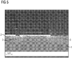
- FIG 5 is a scanning electron microscope image illustrating selective formation of porous silicon 3 volume.
- Semiconductive silicon layer 1 in the following, the term “silicon” may be used for semiconductive silicon layer
- Si 3 N 4 mask 2 The porous silicon 3 volume is formed by etching in silicon.
- An electric field is set over the structure comprising semiconductive silicon layer 1 and mask 2. Then hydrogen fluoride based etching fluid (such as in particular mixture of hydrogen fluoride and ethanol) is introduced into silicon layer 1.
- the etching fluid creates a porous structure (i.e. porous volume 3) in the silicon layer 1, whereby the channels formed by the etching fluid tend to follow the electric field lines i.e. they are directed by the electric field lines.
- FIG 6 illustrates the manufacture of porous silicon 3 volume by self-limiting etching (the image on the left is a SEM image and the image on the right is a magnification showing details of the etched channels porosity forming).
- the silicon structure comprises in addition to the semiconducting silicon layer 1 also an electrically insulating layer 4 (which may be a BOX layer and/or a SiO 2 layer and/or a SiN layer) limiting to the semiconductive silicon layer 1.
- the porous silicon 3 volume is formed in the semiconductive silicon layer 1 in a self-limiting manner such that the porous silicon 3 limits to the electrically insulating layer 4.
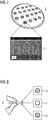
- FIG 7 illustrates SOI wafer 5 after porous silicon etching in SOI wafer 5.
- Under SOI wafer 5 is a SEM image of the SOI wafer 5 showing the structure of porous silicon 3. AS can be seen, porous silicon 3 was formed by selective formation method.
- FIG 9 shows porous silicon 3 in larger magnification.
- FIG 10 shows coated porous silicon 9.
- FIG 11 is a Ragone plot for various materials.
- FIG 12 and 14 illustrate two-electrode measurements for samples 8 sample M47 ( FIG 12 , NaCl) and for sample M50 ( FIG 13 , TEABF4/PC). The same measurement principle was used in measurements shown in FIG 10 to 20 .
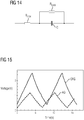
- FIG 14 illustrates a simplified equivalent circuit for the samples.
- the sample 8 has as its equivalent series resistance R ESR and a leak resistance R Leak .
- FIG 15 shows galvanostatic charge-discharge curves for samples M47 (A) and M50 (0).
- FIG 16 shows a theoretical cyclic voltammetry curve for a 3 F EDLC in series with a 50 m ⁇ ESR.
- FIG 17 shows a real (measured) cyclic voltammetry curve for a 3 F EDLC in series with a 50 m ⁇ ESR.
- FIG 18 shows a measured cyclic voltammetry curve for a sample 8 with porous silicon electrodes without coating (i.e. formed of porous silicon 3) initially and after two weeks.
- porous silicon electrodes 3 may not so regarded as very stable and they may therefore be only limitedly suitable for long-term applications.
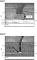
- FIG 21 is a SEM image in which trench 10 in SOI layer 11 that has been manufactured by plasma etching is in n+ Si wafer 14. Shown are also BOX layer 12 and handle layer 13.
- FIG 22 is a SEM image in which trench 10 in SOI layer 11 that has been manufactured by plasma etching is in n- Si wafer 14'.
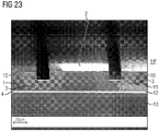
- FIG 23 is a SEM image illustrating a section of a cylindrical trench in a highly doped n+ SOI wafer. As can be seen, with plasma etching we are able to obtain vertical walls having almost rectangular shape. This helps us to manufacture well-defined porous silicon structures.
- FIG 24 shows half of a section of a first blank 17a and half of a section of a second blank 17b. Both blanks 17a, 17b are our proof-of concept test devices.
- Blank 17a is based on (n++ or p++ doped) DSP SOI wafer 14'''.
- the trench 10 has been formed by using the methods described above, and is limited at its bottom to the BOX layer.
- the porous silicon 3 has been coated with TiN by using ALD to form coated porous silicon 9.
- Contacting points 18, 19 go through the BOX layer 12 and also the SOI layer 11 and therefore enable contacting in or on the SOI layer 11. This facilitates integrating the blank 17a to an in-chip structure that also comprises further microelectronic components.
- Blank 17b which is an alternative to blank 17a, is based on (n++ or p++ doped) DSP Si wafer 14''''.
- the semiconductive silicon layer 1 is limited to SiN layer 15 which has LTO layer, a PSi layer, or a metal layer on top of it.
- FIG 25 illustrates trenches 10 etched from the backside of a handle wafer 14'''''.
- the handle wafer 14''''' may in particular be n++ or p++ doped DSP SOI wafer ''' or highly doped n+ SOI wafer 14".
- the handle wafer 14'''''' comprises a number of blanks 17 which may be blanks 17a.
- the handle wafer 14''''' may further comprise other microelectric components thank blanks 17.
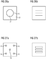
- FIG 26a and 26b illustrate the handle wafer 14''''' after cleaving into separate chips (blanks 17 and other microelectric components 20), from the handle layer 13 side, and FIG 27a and 27b from the SOI layer 11 side, respectively.
- the trench 10 divides the blank 17 in two volumes: first volume 22 which is laterally the outer volume surrounds second volume 21 which is laterally the inner volume.
- Contacting points 18 (which may be in any number, from one to a very large number) are contacted to the first volume 22.
- Contacting points 19 (which may be in any number, from one to a very large number) are contacted to the second volume 21.
- FIG 28 illustrates supercapacitor 25 that has been manufactured from blank 17a by adding electrolyte 24 into trench 10 and fastening 23 sealing lid to close the trench 10 from the top so that electrolyte 24 does not escape from the supercapacitor 29.
- FIG 29 illustrates supercapacitor 25 that has been manufactured from blank 17b by adding electrolyte 24 into trench 10 and fastening 23 sealing lid to close the trench 10 from the top so that electrolyte 24 does not escape from the supercapacitor 25.
- Both supercapacitors 25 may comprise further microelectronic devices 26. At least some of the microelectronic devices 26 are preferably in the SOI layer 26 of the supercapacitor 25 if the supercapacitor 25 has been manufactured from blank 17b.
- FIG 30a illustrates contacting points 18, 19 as seen from top. They are surrounded by LTO/pSi/metal layer 16 or by SOI layer 11.
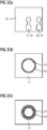
- FIG 30b and 30c illustrate trench 10 as seen from below, the trench 10 separating the first volume 22 (i.e. the laterally outer volume) from the second volume 21 (i.e. the laterally inner volume).
- the trench 10 may have any closed shape, as explained above, provided that the porous semiconductor volumes on the opposite sides of the trench are electrically isolated from each other so that the electrodes of the supercapasitor will not be short-circuited.
- FIG 31 is a SEM image of deep etched trenches 10 in semiconductive silicon layer 1. The image on the right side with larger magnification.
- FIG 32 is a SEM image of deep etching the trench 10 in porous silicon 3.
- the image on left bottom is with a larger magnification and on the right side with still larger magnification.
- the trench 10 has been made in the handle layer 13 of a handle wafer 14'''''.
- FIG 33 illustrates removal of porous silicon 3 from the bottom of the trenches 10. Porous silicon may be need to be removed after etching, in particular if the bottom of trench 10 as shown FIG 32 would not suffice.
- FIG 34 illustrates porous silicon 3 on the sidewalls of the trench 10 and at the end of the channels i.e. at the interface of porous silicon 3 and semiconductive silicon layer 1 (such as, the SOI layer 11).
- FIG 35 illustrates deposition of TiN by atomic layer deposition.
- the image on the bottom is with larger magnification and the third image with even larger magnification.
- the sidewalls of trench 10 are coated with TiN (i.e. coated porous silicon 9).
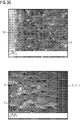
- FIG 36 is a SEM image of TiN coated PS as in FIG 35 in still larger magnification.
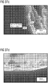
- FIG 37a to 37d illustrate removal of TiN from the bottom of the trench 10.
- FIG 37a illustrates the trench sidewall and FIG 37b the trench bottom with about 78 nm TiN layer.
- FIG 37c illustrates the trench sidewall and FIG 37d the trench bottom after TiN has been removed from the bottom of the trench 10 by plasma etching
- FIG 38 illustrates a sample holder used to carry out the measurements
- FIG 39a and 39b illustrate measured cyclic voltammetry curves of certain supercapacitors that were made inside a silicon wafer.
- FIG 39a shows the measurement results of supercapacitor with ALD TiN coating and without the porous silicon volumes.
- the supercapacitor has a capacitance of 4 ⁇ F.
- FIG 39b shows the measurement results of supercapacitor with ALD TiN coating and with the porous silicon volumes.
- the supercapacitor 25 has a capacitance of 140 ⁇ F.
- supercapacitor 25 may open new possibilities for miniaturized and integrated energy storage.
- Electrochemical double layer capacitors (EDLC), commonly called as supercapacitors, offer an attractive possibility for short term high power energy storage that could be utilised also in miniaturized devices.
- On-chip or in-chip integration of supercapacitor elements by utilising large-area silicon nanostructures, like porous silicon (PS), may provide a scalable on-chip solution.
- PS porous silicon
- Such candidates include: NbN and electrically conducting oxides.
- electrolyte 24 instead or in addition to water-based electrolytes or organic (liquid) electrolytes, a solid electrolyte, such as TiO 2 may be used.
- the in-wafer supercapacitors can be easily connected in series or parallel to vary the voltage or total capacitance.
Landscapes
- Engineering & Computer Science (AREA)
- Power Engineering (AREA)
- Microelectronics & Electronic Packaging (AREA)
- Manufacturing & Machinery (AREA)
- Chemical & Material Sciences (AREA)
- Materials Engineering (AREA)
- Semiconductor Memories (AREA)
- Semiconductor Integrated Circuits (AREA)
- Electric Double-Layer Capacitors Or The Like (AREA)
Claims (15)
- Rohling (17, 17a, 17b), der zur Verwendung als Körper eines Superkondensators (25) geeignet ist, umfassend ein erstes poröses Halbleitervolumen (22) und ein zweites poröses Halbleitervolumen (21),
wobei das zweite poröse Halbleitervolumen (21) von dem ersten porösen Halbleitervolumen (22) durch einen Trench (10) getrennt ist, der zur Aufnahme eines Elektrolyten (24) geeignet ist, und
die ersten und zweiten porösen Halbleitervolumen (22, 21) Kanäle umfassen, die sich zum Trench (10) hin öffnen, dadurch gekennzeichnet, dass das zweite poröse Halbleitervolumen (21) lateral von dem ersten porösen Halbleitervolumen (22) umgeben ist und der Trench (10) eine geschlossene Form bildet. - Rohling (17, 17a, 17b) nach Anspruch 1, wobei: das erste poröse Halbleitervolumen (22) und das zweite poröse Halbleitervolumen (21) sich in derselben Halbleiterschicht (1, 13) befinden und wobei die ersten und zweiten porösen Halbleitervolumen (22, 21) sich über die Höhe der Schicht (1, 13) erstrecken.
- Rohling (17, 17a, 17b) nach Anspruch 1 oder 2, wobei: die Seitenkante des Trenchs (10) des ersten porösen Halbleitervolumens (22) und die Seitenkante des Trenchs (10) des zweiten porösen Halbleitervolumens (21) jeweils mindestens eine Elektrode bilden.
- Rohling (17, 17a, 17b) nach Anspruch 3, wobei: mindestens eine, beide oder alle der Elektroden die jeweiligen Kanten zumindest teilweise beschichtet haben, so dass sie beschichtete poröse Halbleiter sind oder umfassen.
- Rohling (17, 17a, 17b) nach Anspruch 4, wobei: die Beschichtung TiN, NbN oder mindestens ein elektrisch leitendes Oxid oder Metall ist oder umfasst.
- Rohling (17, 17a, 17b) nach einem der vorstehenden Ansprüche, wobei: das erste poröse Halbleitervolumen (22) und das zweite poröse Halbleitervolumen (21) Silizium sind oder umfassen.
- Rohling (17, 17a, 17b) nach einem der vorstehenden Ansprüche, wobei: der Rohling (17, 17a, 17b) weiter eine Isolierschicht (12, 15) umfasst, die auf den Boden des ersten porösen Halbleitervolumens (22) und des zweiten porösen Halbleitervolumens (21) und zum Boden des Trenchs (10) begrenzt ist.
- Rohling (17, 17a, 17b) nach Anspruch 5 und 6, wobei: die Isolierschicht (12, 15) eine eingebettete Oxidschicht (12) ist oder umfasst und/oder aus Halbleiteroxid besteht und/oder eine elektrische Isolierschicht umfasst, die insbesondere eine Siliziumnitridschicht (15) sein kann.
- Rohling (17, 17b) nach einem der vorstehenden Ansprüche, wobei: der Rohling (17, 17b) in einem ein- oder doppelseitig polierten Siliziumwafer ist und das erste poröse Halbleitervolumen (22) und das zweite poröse Halbleitervolumen (21) in einer halbleitenden Siliziumschicht (1, 13) gebildet worden sind, wobei der einseitig oder doppelseitig polierte Siliziumwafer n++ oder p++ dotiert sein kann.
- Rohling (17, 17b) nach Anspruch 9, wobei: der Trench (10) von unten durch eine Siliziumnitridschicht oder eine BOX-Schicht (12) begrenzt ist, die als eine Dichtung wirkt.
- Rohling (17, 17a) nach einem der vorstehenden Ansprüche 1 bis 10, wobei:a) der Rohling (17, 17a) in einem ein- oder doppelseitig polierten Silizium-auf-Isolator-Wafer (14, 14''', 14''''') ist und das erste poröse Halbleitervolumen (22) und das zweite poröse Halbleitervolumen (21) in der Griffschicht (13) gebildet worden sind, wodurch der ein- oder doppelseitig polierte Silizium-auf-Isolator (14, 14''', 14''''') Wafer n++ oder p++ dotiert sein kann;
oderb) der Rohling (17, 17a, 17b) in einem ein- oder doppelseitigen polierten Siliziumwafer (14, 14,", 14''', 14''''') ist, der ein Silizium-auf-Isolator-Wafer ist, der eine Silizium-auf-Isolator-Schicht (11) auf der der Silizium-auf-Isolator-Schicht (11) gegenüberliegenden Seite umfasst. - Superkondensator (25) umfassend: einen Körper, der unter Verwendung eines Rohlings (17, 17a, 17b) nach einem der vorstehenden Ansprüche gebildet ist, so dass das erste poröse Halbleitervolumen (22) als eine Elektrode wirkt und das zweite poröse Halbleitervolumen (21) als eine andere Elektrode wirkt, mit einem Elektrolyten (24) im Trench (10).
- Superkondensator (25) nach Anspruch 12, wobei: der Superkondensator (25) weiter elektrische Kontaktpunkte (18, 19) zu den Elektroden umfasst, die durch eine Schicht (12, 15) hergestellt wurden, die sich unmittelbar unter dem Trench (10) befindet.
- Superkondensator (25) nach Anspruch 12 oder 13, weiter umfassend: einen Dichtungsdeckel (23) zum Abdichten des Trenchs (10), der vorzugsweise konfiguriert ist, um den Trench (10) nur von oben abzudichten.
- Superkondensator (25) nach einem der Ansprüche 12 bis 14, wobei: der Superkondensator (25) ein separatorloser Superkondensator ist, bei dem sich kein dazwischenliegender Separator oder Separator in dem Trench befindet, sondern der Trench (10) selbst als Separator wirkt.
Applications Claiming Priority (2)
| Application Number | Priority Date | Filing Date | Title |
|---|---|---|---|
| FI20145914 | 2014-10-17 | ||
| PCT/FI2015/050692 WO2016059296A1 (en) | 2014-10-17 | 2015-10-14 | A blank suitable for use as a body of supercapacitor, a supercapacitor, and a method of manufacturing a porous silicon volume |
Publications (2)
| Publication Number | Publication Date |
|---|---|
| EP3207553A1 EP3207553A1 (de) | 2017-08-23 |
| EP3207553B1 true EP3207553B1 (de) | 2019-12-04 |
Family
ID=54477002
Family Applications (1)
| Application Number | Title | Priority Date | Filing Date |
|---|---|---|---|
| EP15791002.7A Active EP3207553B1 (de) | 2014-10-17 | 2015-10-14 | Zuschnitt zur verwendung als körper eines superkondensators und superkondensator |
Country Status (6)
| Country | Link |
|---|---|
| US (1) | US10410798B2 (de) |
| EP (1) | EP3207553B1 (de) |
| JP (2) | JP2017535076A (de) |
| KR (1) | KR102043806B1 (de) |
| CN (1) | CN107683516A (de) |
| WO (1) | WO2016059296A1 (de) |
Families Citing this family (3)
| Publication number | Priority date | Publication date | Assignee | Title |
|---|---|---|---|---|
| NO343382B1 (en) | 2017-03-07 | 2019-02-18 | Univ College Of Southeast Norway | On-chip supercapacitor With Silicon nanostructure |
| EP3593371B1 (de) | 2017-03-07 | 2021-05-19 | University of South-Eastern Norway | Abgeschiedener kohlenstofffilm auf geätztem silicium für on-chip-superkondensator |
| US20240158944A1 (en) * | 2022-11-16 | 2024-05-16 | Applied Materials, Inc. | Porous chamber component coating augmented with colloids |
Family Cites Families (16)
| Publication number | Priority date | Publication date | Assignee | Title |
|---|---|---|---|---|
| FR2672731A1 (fr) * | 1991-02-07 | 1992-08-14 | France Telecom | Procede d'oxydation localisee enterree d'un substrat de silicium et circuit integre correspondant. |
| US5508542A (en) * | 1994-10-28 | 1996-04-16 | International Business Machines Corporation | Porous silicon trench and capacitor structures |
| JP2004103613A (ja) * | 2002-09-04 | 2004-04-02 | Toshiba Corp | 半導体装置とその製造方法 |
| DE10306129A1 (de) | 2003-02-14 | 2004-08-26 | Robert Bosch Gmbh | Verfahren zur Herstellung eines Bauelementes mit einem Halbleiterträger sowie Bauelement |
| US20070048589A1 (en) | 2005-08-30 | 2007-03-01 | Koripella Chowdary R | Integrated micro fuel cell apparatus |
| US7161228B1 (en) | 2005-12-28 | 2007-01-09 | Analog Devices, Inc. | Three-dimensional integrated capacitance structure |
| TW200828607A (en) * | 2006-12-11 | 2008-07-01 | Fujikura Ltd | Photoelectric conversion element |
| US20100221606A1 (en) | 2009-03-02 | 2010-09-02 | Omkaram Nalamasu | Energy storage device with porous electrode |
| JP5563091B2 (ja) | 2009-10-30 | 2014-07-30 | ウィリアム マーシュ ライス ユニバーシティ | 構造化されたシリコン電池アノード |
| JP5743353B2 (ja) | 2010-04-02 | 2015-07-01 | インテル・コーポレーション | 電荷蓄積デバイス、電荷蓄積デバイスを製造する方法、移動型電子デバイスおよびマイクロ電子デバイス |
| US8841030B2 (en) * | 2012-01-24 | 2014-09-23 | Enovix Corporation | Microstructured electrode structures |
| US9978533B2 (en) | 2012-02-21 | 2018-05-22 | Intel Corporation | Energy storage device, method of manufacturing same, and mobile electronic device containing same |
| WO2013128082A1 (en) | 2012-02-28 | 2013-09-06 | Teknologian Tutkimuskeskus Vtt | Integrable electrochemical capacitor |
| WO2013162546A1 (en) | 2012-04-25 | 2013-10-31 | Intel Corporation | Energy storage device, method of manufacturing same, and mobile electronic device containing same |
| US9093226B2 (en) * | 2012-09-17 | 2015-07-28 | Intel Corporation | Energy storage device, method of manufacturing same, and mobile electronic device containing same |
| US8816465B1 (en) * | 2013-02-22 | 2014-08-26 | Intel Corporation | Energy conversion and storage device and mobile electronic device containing same |
-
2015
- 2015-10-14 WO PCT/FI2015/050692 patent/WO2016059296A1/en not_active Ceased
- 2015-10-14 KR KR1020177012987A patent/KR102043806B1/ko not_active Expired - Fee Related
- 2015-10-14 CN CN201580068972.7A patent/CN107683516A/zh active Pending
- 2015-10-14 US US15/518,774 patent/US10410798B2/en not_active Expired - Fee Related
- 2015-10-14 JP JP2017520521A patent/JP2017535076A/ja active Pending
- 2015-10-14 EP EP15791002.7A patent/EP3207553B1/de active Active
-
2019
- 2019-01-25 JP JP2019010721A patent/JP2019096893A/ja active Pending
Non-Patent Citations (1)
| Title |
|---|
| None * |
Also Published As
| Publication number | Publication date |
|---|---|
| US20170229252A1 (en) | 2017-08-10 |
| US10410798B2 (en) | 2019-09-10 |
| JP2017535076A (ja) | 2017-11-24 |
| KR102043806B1 (ko) | 2019-11-12 |
| CN107683516A (zh) | 2018-02-09 |
| WO2016059296A1 (en) | 2016-04-21 |
| JP2019096893A (ja) | 2019-06-20 |
| EP3207553A1 (de) | 2017-08-23 |
| KR20170069270A (ko) | 2017-06-20 |
Similar Documents
| Publication | Publication Date | Title |
|---|---|---|
| US10777366B2 (en) | Method of increasing an energy density and an achievable power output of an energy storage device | |
| Ortaboy et al. | MnO x-decorated carbonized porous silicon nanowire electrodes for high performance supercapacitors | |
| US8503161B1 (en) | Supercapacitor cells and micro-supercapacitors | |
| Achour et al. | Hierarchical nanocomposite electrodes based on titanium nitride and carbon nanotubes for micro-supercapacitors | |
| US9640332B2 (en) | Hybrid electrochemical capacitor | |
| Gardner et al. | Integrated on-chip energy storage using passivated nanoporous-silicon electrochemical capacitors | |
| Burchak et al. | Scalable chemical synthesis of doped silicon nanowires for energy applications | |
| Cao et al. | Quantitative investigation on the effect of hydrogenation on the performance of MnO 2/H-TiO 2 composite electrodes for supercapacitors | |
| US10249444B2 (en) | Method of fabricating an electrochemical double-layer capacitor | |
| US10410798B2 (en) | Blank suitable for use as a body of a supercapacitor, a supercapacitor, and a method of manufacturing a porous silicon volume | |
| TW201349267A (zh) | 集成能量儲存裝置至微電子裝置及行動裝置之基底上的技術 | |
| CN104115246B (zh) | 能量储存装置、能量储存装置的制造方法以及包含能量储存装置的移动电子装置 | |
| Ahmed et al. | On-silicon supercapacitors with enhanced storage performance | |
| EP3067313A1 (de) | Elektrodenmaterial mit siliciumnanodrähten, die mit mesoporöser oxidnanostrukturschicht beschichtet sind, und ionische liguidelektrolyten für energiespeicheranwendungen | |
| Thissandier et al. | Highly N-doped silicon nanowires as a possible alternative to carbon for on-chip electrochemical capacitors | |
| Zhang et al. | 3D reticulate Co x Ni 3− x S 2 nanostructure on nickel foam as a new type of electroactive material for high-performance supercapacitors | |
| Grigoras et al. | Porous silicon electrodes for high performance integrated supercapacitors | |
| KR102754362B1 (ko) | Se 복합 CuO/Ni3V2O8 나노시트 및 이를 포함하는 에너지 저장 장치 | |
| McSweeney et al. | Pseudocapacitive charge storage at nanoscale silicon electrodes | |
| Gómez-Romero et al. | Electrode material comprising silicon nanowires covered by a mesoporous oxide nanostructured coating and ionic liquid electrolytes for energy storage applications |
Legal Events
| Date | Code | Title | Description |
|---|---|---|---|
| STAA | Information on the status of an ep patent application or granted ep patent |
Free format text: STATUS: THE INTERNATIONAL PUBLICATION HAS BEEN MADE |
|
| PUAI | Public reference made under article 153(3) epc to a published international application that has entered the european phase |
Free format text: ORIGINAL CODE: 0009012 |
|
| STAA | Information on the status of an ep patent application or granted ep patent |
Free format text: STATUS: REQUEST FOR EXAMINATION WAS MADE |
|
| 17P | Request for examination filed |
Effective date: 20170418 |
|
| AK | Designated contracting states |
Kind code of ref document: A1 Designated state(s): AL AT BE BG CH CY CZ DE DK EE ES FI FR GB GR HR HU IE IS IT LI LT LU LV MC MK MT NL NO PL PT RO RS SE SI SK SM TR |
|
| AX | Request for extension of the european patent |
Extension state: BA ME |
|
| DAV | Request for validation of the european patent (deleted) | ||
| DAX | Request for extension of the european patent (deleted) | ||
| STAA | Information on the status of an ep patent application or granted ep patent |
Free format text: STATUS: EXAMINATION IS IN PROGRESS |
|
| 17Q | First examination report despatched |
Effective date: 20181029 |
|
| GRAP | Despatch of communication of intention to grant a patent |
Free format text: ORIGINAL CODE: EPIDOSNIGR1 |
|
| STAA | Information on the status of an ep patent application or granted ep patent |
Free format text: STATUS: GRANT OF PATENT IS INTENDED |
|
| INTG | Intention to grant announced |
Effective date: 20190705 |
|
| GRAS | Grant fee paid |
Free format text: ORIGINAL CODE: EPIDOSNIGR3 |
|
| GRAA | (expected) grant |
Free format text: ORIGINAL CODE: 0009210 |
|
| STAA | Information on the status of an ep patent application or granted ep patent |
Free format text: STATUS: THE PATENT HAS BEEN GRANTED |
|
| AK | Designated contracting states |
Kind code of ref document: B1 Designated state(s): AL AT BE BG CH CY CZ DE DK EE ES FI FR GB GR HR HU IE IS IT LI LT LU LV MC MK MT NL NO PL PT RO RS SE SI SK SM TR |
|
| REG | Reference to a national code |
Ref country code: GB Ref legal event code: FG4D |
|
| REG | Reference to a national code |
Ref country code: CH Ref legal event code: EP |
|
| REG | Reference to a national code |
Ref country code: AT Ref legal event code: REF Ref document number: 1210431 Country of ref document: AT Kind code of ref document: T Effective date: 20191215 |
|
| REG | Reference to a national code |
Ref country code: DE Ref legal event code: R096 Ref document number: 602015043083 Country of ref document: DE |
|
| REG | Reference to a national code |
Ref country code: IE Ref legal event code: FG4D |
|
| REG | Reference to a national code |
Ref country code: NL Ref legal event code: MP Effective date: 20191204 |
|
| REG | Reference to a national code |
Ref country code: LT Ref legal event code: MG4D |
|
| PG25 | Lapsed in a contracting state [announced via postgrant information from national office to epo] |
Ref country code: GR Free format text: LAPSE BECAUSE OF FAILURE TO SUBMIT A TRANSLATION OF THE DESCRIPTION OR TO PAY THE FEE WITHIN THE PRESCRIBED TIME-LIMIT Effective date: 20200305 Ref country code: SE Free format text: LAPSE BECAUSE OF FAILURE TO SUBMIT A TRANSLATION OF THE DESCRIPTION OR TO PAY THE FEE WITHIN THE PRESCRIBED TIME-LIMIT Effective date: 20191204 Ref country code: LV Free format text: LAPSE BECAUSE OF FAILURE TO SUBMIT A TRANSLATION OF THE DESCRIPTION OR TO PAY THE FEE WITHIN THE PRESCRIBED TIME-LIMIT Effective date: 20191204 Ref country code: FI Free format text: LAPSE BECAUSE OF FAILURE TO SUBMIT A TRANSLATION OF THE DESCRIPTION OR TO PAY THE FEE WITHIN THE PRESCRIBED TIME-LIMIT Effective date: 20191204 Ref country code: BG Free format text: LAPSE BECAUSE OF FAILURE TO SUBMIT A TRANSLATION OF THE DESCRIPTION OR TO PAY THE FEE WITHIN THE PRESCRIBED TIME-LIMIT Effective date: 20200304 Ref country code: LT Free format text: LAPSE BECAUSE OF FAILURE TO SUBMIT A TRANSLATION OF THE DESCRIPTION OR TO PAY THE FEE WITHIN THE PRESCRIBED TIME-LIMIT Effective date: 20191204 Ref country code: NO Free format text: LAPSE BECAUSE OF FAILURE TO SUBMIT A TRANSLATION OF THE DESCRIPTION OR TO PAY THE FEE WITHIN THE PRESCRIBED TIME-LIMIT Effective date: 20200304 |
|
| PG25 | Lapsed in a contracting state [announced via postgrant information from national office to epo] |
Ref country code: RS Free format text: LAPSE BECAUSE OF FAILURE TO SUBMIT A TRANSLATION OF THE DESCRIPTION OR TO PAY THE FEE WITHIN THE PRESCRIBED TIME-LIMIT Effective date: 20191204 Ref country code: HR Free format text: LAPSE BECAUSE OF FAILURE TO SUBMIT A TRANSLATION OF THE DESCRIPTION OR TO PAY THE FEE WITHIN THE PRESCRIBED TIME-LIMIT Effective date: 20191204 |
|
| PG25 | Lapsed in a contracting state [announced via postgrant information from national office to epo] |
Ref country code: AL Free format text: LAPSE BECAUSE OF FAILURE TO SUBMIT A TRANSLATION OF THE DESCRIPTION OR TO PAY THE FEE WITHIN THE PRESCRIBED TIME-LIMIT Effective date: 20191204 |
|
| PG25 | Lapsed in a contracting state [announced via postgrant information from national office to epo] |
Ref country code: NL Free format text: LAPSE BECAUSE OF FAILURE TO SUBMIT A TRANSLATION OF THE DESCRIPTION OR TO PAY THE FEE WITHIN THE PRESCRIBED TIME-LIMIT Effective date: 20191204 Ref country code: PT Free format text: LAPSE BECAUSE OF FAILURE TO SUBMIT A TRANSLATION OF THE DESCRIPTION OR TO PAY THE FEE WITHIN THE PRESCRIBED TIME-LIMIT Effective date: 20200429 Ref country code: EE Free format text: LAPSE BECAUSE OF FAILURE TO SUBMIT A TRANSLATION OF THE DESCRIPTION OR TO PAY THE FEE WITHIN THE PRESCRIBED TIME-LIMIT Effective date: 20191204 Ref country code: RO Free format text: LAPSE BECAUSE OF FAILURE TO SUBMIT A TRANSLATION OF THE DESCRIPTION OR TO PAY THE FEE WITHIN THE PRESCRIBED TIME-LIMIT Effective date: 20191204 Ref country code: CZ Free format text: LAPSE BECAUSE OF FAILURE TO SUBMIT A TRANSLATION OF THE DESCRIPTION OR TO PAY THE FEE WITHIN THE PRESCRIBED TIME-LIMIT Effective date: 20191204 Ref country code: ES Free format text: LAPSE BECAUSE OF FAILURE TO SUBMIT A TRANSLATION OF THE DESCRIPTION OR TO PAY THE FEE WITHIN THE PRESCRIBED TIME-LIMIT Effective date: 20191204 |
|
| PG25 | Lapsed in a contracting state [announced via postgrant information from national office to epo] |
Ref country code: SM Free format text: LAPSE BECAUSE OF FAILURE TO SUBMIT A TRANSLATION OF THE DESCRIPTION OR TO PAY THE FEE WITHIN THE PRESCRIBED TIME-LIMIT Effective date: 20191204 Ref country code: IS Free format text: LAPSE BECAUSE OF FAILURE TO SUBMIT A TRANSLATION OF THE DESCRIPTION OR TO PAY THE FEE WITHIN THE PRESCRIBED TIME-LIMIT Effective date: 20200404 Ref country code: SK Free format text: LAPSE BECAUSE OF FAILURE TO SUBMIT A TRANSLATION OF THE DESCRIPTION OR TO PAY THE FEE WITHIN THE PRESCRIBED TIME-LIMIT Effective date: 20191204 |
|
| REG | Reference to a national code |
Ref country code: DE Ref legal event code: R097 Ref document number: 602015043083 Country of ref document: DE |
|
| REG | Reference to a national code |
Ref country code: AT Ref legal event code: MK05 Ref document number: 1210431 Country of ref document: AT Kind code of ref document: T Effective date: 20191204 |
|
| PLBE | No opposition filed within time limit |
Free format text: ORIGINAL CODE: 0009261 |
|
| STAA | Information on the status of an ep patent application or granted ep patent |
Free format text: STATUS: NO OPPOSITION FILED WITHIN TIME LIMIT |
|
| PG25 | Lapsed in a contracting state [announced via postgrant information from national office to epo] |
Ref country code: DK Free format text: LAPSE BECAUSE OF FAILURE TO SUBMIT A TRANSLATION OF THE DESCRIPTION OR TO PAY THE FEE WITHIN THE PRESCRIBED TIME-LIMIT Effective date: 20191204 |
|
| 26N | No opposition filed |
Effective date: 20200907 |
|
| PG25 | Lapsed in a contracting state [announced via postgrant information from national office to epo] |
Ref country code: PL Free format text: LAPSE BECAUSE OF FAILURE TO SUBMIT A TRANSLATION OF THE DESCRIPTION OR TO PAY THE FEE WITHIN THE PRESCRIBED TIME-LIMIT Effective date: 20191204 Ref country code: SI Free format text: LAPSE BECAUSE OF FAILURE TO SUBMIT A TRANSLATION OF THE DESCRIPTION OR TO PAY THE FEE WITHIN THE PRESCRIBED TIME-LIMIT Effective date: 20191204 Ref country code: AT Free format text: LAPSE BECAUSE OF FAILURE TO SUBMIT A TRANSLATION OF THE DESCRIPTION OR TO PAY THE FEE WITHIN THE PRESCRIBED TIME-LIMIT Effective date: 20191204 |
|
| PG25 | Lapsed in a contracting state [announced via postgrant information from national office to epo] |
Ref country code: IT Free format text: LAPSE BECAUSE OF FAILURE TO SUBMIT A TRANSLATION OF THE DESCRIPTION OR TO PAY THE FEE WITHIN THE PRESCRIBED TIME-LIMIT Effective date: 20191204 |
|
| REG | Reference to a national code |
Ref country code: CH Ref legal event code: PL |
|
| PG25 | Lapsed in a contracting state [announced via postgrant information from national office to epo] |
Ref country code: LU Free format text: LAPSE BECAUSE OF NON-PAYMENT OF DUE FEES Effective date: 20201014 Ref country code: MC Free format text: LAPSE BECAUSE OF FAILURE TO SUBMIT A TRANSLATION OF THE DESCRIPTION OR TO PAY THE FEE WITHIN THE PRESCRIBED TIME-LIMIT Effective date: 20191204 |
|
| REG | Reference to a national code |
Ref country code: BE Ref legal event code: MM Effective date: 20201031 |
|
| PG25 | Lapsed in a contracting state [announced via postgrant information from national office to epo] |
Ref country code: LI Free format text: LAPSE BECAUSE OF NON-PAYMENT OF DUE FEES Effective date: 20201031 Ref country code: CH Free format text: LAPSE BECAUSE OF NON-PAYMENT OF DUE FEES Effective date: 20201031 Ref country code: BE Free format text: LAPSE BECAUSE OF NON-PAYMENT OF DUE FEES Effective date: 20201031 |
|
| PG25 | Lapsed in a contracting state [announced via postgrant information from national office to epo] |
Ref country code: IE Free format text: LAPSE BECAUSE OF NON-PAYMENT OF DUE FEES Effective date: 20201014 |
|
| PGFP | Annual fee paid to national office [announced via postgrant information from national office to epo] |
Ref country code: DE Payment date: 20211020 Year of fee payment: 7 Ref country code: GB Payment date: 20211022 Year of fee payment: 7 |
|
| PGFP | Annual fee paid to national office [announced via postgrant information from national office to epo] |
Ref country code: FR Payment date: 20211022 Year of fee payment: 7 |
|
| PG25 | Lapsed in a contracting state [announced via postgrant information from national office to epo] |
Ref country code: TR Free format text: LAPSE BECAUSE OF FAILURE TO SUBMIT A TRANSLATION OF THE DESCRIPTION OR TO PAY THE FEE WITHIN THE PRESCRIBED TIME-LIMIT Effective date: 20191204 Ref country code: MT Free format text: LAPSE BECAUSE OF FAILURE TO SUBMIT A TRANSLATION OF THE DESCRIPTION OR TO PAY THE FEE WITHIN THE PRESCRIBED TIME-LIMIT Effective date: 20191204 Ref country code: CY Free format text: LAPSE BECAUSE OF FAILURE TO SUBMIT A TRANSLATION OF THE DESCRIPTION OR TO PAY THE FEE WITHIN THE PRESCRIBED TIME-LIMIT Effective date: 20191204 |
|
| PG25 | Lapsed in a contracting state [announced via postgrant information from national office to epo] |
Ref country code: MK Free format text: LAPSE BECAUSE OF FAILURE TO SUBMIT A TRANSLATION OF THE DESCRIPTION OR TO PAY THE FEE WITHIN THE PRESCRIBED TIME-LIMIT Effective date: 20191204 |
|
| REG | Reference to a national code |
Ref country code: DE Ref legal event code: R119 Ref document number: 602015043083 Country of ref document: DE |
|
| GBPC | Gb: european patent ceased through non-payment of renewal fee |
Effective date: 20221014 |
|
| PG25 | Lapsed in a contracting state [announced via postgrant information from national office to epo] |
Ref country code: FR Free format text: LAPSE BECAUSE OF NON-PAYMENT OF DUE FEES Effective date: 20221031 Ref country code: DE Free format text: LAPSE BECAUSE OF NON-PAYMENT OF DUE FEES Effective date: 20230503 |
|
| PG25 | Lapsed in a contracting state [announced via postgrant information from national office to epo] |
Ref country code: GB Free format text: LAPSE BECAUSE OF NON-PAYMENT OF DUE FEES Effective date: 20221014 |