EP3204754B1 - Kalibrierungsvorrichtung und verwendungen davon - Google Patents
Kalibrierungsvorrichtung und verwendungen davon Download PDFInfo
- Publication number
- EP3204754B1 EP3204754B1 EP15848546.6A EP15848546A EP3204754B1 EP 3204754 B1 EP3204754 B1 EP 3204754B1 EP 15848546 A EP15848546 A EP 15848546A EP 3204754 B1 EP3204754 B1 EP 3204754B1
- Authority
- EP
- European Patent Office
- Prior art keywords
- axis
- waveplate
- quarter
- waveplates
- retardation
- Prior art date
- Legal status (The legal status is an assumption and is not a legal conclusion. Google has not performed a legal analysis and makes no representation as to the accuracy of the status listed.)
- Active
Links
Images


Classifications
-
- G—PHYSICS
- G01—MEASURING; TESTING
- G01N—INVESTIGATING OR ANALYSING MATERIALS BY DETERMINING THEIR CHEMICAL OR PHYSICAL PROPERTIES
- G01N21/00—Investigating or analysing materials by the use of optical means, i.e. using sub-millimetre waves, infrared, visible or ultraviolet light
- G01N21/17—Systems in which incident light is modified in accordance with the properties of the material investigated
- G01N21/19—Dichroism
-
- G—PHYSICS
- G01—MEASURING; TESTING
- G01N—INVESTIGATING OR ANALYSING MATERIALS BY DETERMINING THEIR CHEMICAL OR PHYSICAL PROPERTIES
- G01N21/00—Investigating or analysing materials by the use of optical means, i.e. using sub-millimetre waves, infrared, visible or ultraviolet light
- G01N21/17—Systems in which incident light is modified in accordance with the properties of the material investigated
- G01N21/25—Colour; Spectral properties, i.e. comparison of effect of material on the light at two or more different wavelengths or wavelength bands
- G01N21/27—Colour; Spectral properties, i.e. comparison of effect of material on the light at two or more different wavelengths or wavelength bands using photo-electric detection ; circuits for computing concentration
- G01N21/274—Calibration, base line adjustment, drift correction
-
- G—PHYSICS
- G01—MEASURING; TESTING
- G01N—INVESTIGATING OR ANALYSING MATERIALS BY DETERMINING THEIR CHEMICAL OR PHYSICAL PROPERTIES
- G01N21/00—Investigating or analysing materials by the use of optical means, i.e. using sub-millimetre waves, infrared, visible or ultraviolet light
- G01N21/17—Systems in which incident light is modified in accordance with the properties of the material investigated
- G01N21/21—Polarisation-affecting properties
Definitions
- This invention relates to a device for calibrating circular or linear dichroism spectrometers, or other photoelastic modulator (PEM) based devices or instruments.
- PEM photoelastic modulator
- the invention also relates to methods of calibrating circular or linear dichroism spectrometers using said device.
- Circular dichroism (CD) spectroscopy is a spectroscopic technique where the CD of molecules is measured over a range of wavelengths. CD spectroscopy is used extensively to study chiral molecules of all types and sizes, and finds important applications in the study of large biological molecules. A primary use is in analyzing the higher order structure or conformation of macromolecules, particularly proteins. As higher order structure, for example secondary structure, is sensitive to its environment, temperature or pH, circular dichroism can be used to observe how the structure changes with environmental conditions or on interaction with other molecules. Structural, kinetic and thermodynamic information about macromolecules can be derived from circular dichroism spectroscopy.
- CD calibration is required to ensure that measured CD spectra have the correct magnitude.
- Various factors affect measured CD magnitude including optical imperfections in the instrument, detector non-linearity, detector polarization bias response, gains (AC and DC) in the electronic detection chain and photoelastic modulator (PEM) calibration.
- CD calibration should correct for all of these error contributions across the entire wavelength range of the instrument. Calibration of CD instruments currently depends upon the use of chemical samples prepared to a prescribed concentration and measured in a cell of defined pathlength.
- the present invention provides improved devices for dichroism measurements.
- the present inventors have found that by combining tilted isotropic plates (isoplates) with waveplates of known retardance, it is possible to produce a device which presents an effective differential transmission to left and right circularly polarized states, rather than to linear polarized states.
- the present invention features a device for calibrating circular dichroism or linear dichroism spectrometers, or other photoelastic modulator based devices or instruments, comprising a combination of quarter waveplates (Q) providing (n ⁇ 1/4) waves of retardation at a defined set of wavelengths and isotropic plates (P)
- Q quarter waveplates
- P isotropic plates
- the device further comprises at least one waveplate (H) providing (N ⁇ 1/2) waves of retardation at the same wavelengths where Q provides (n ⁇ 1/4) waves of retardation.
- H waveplate
- the waveplate (Q) has a thickness (t).
- the waveplate (H) has a thickness (2 + 4m)t. In another further embodiment of any one of the above aspects, the waveplate (H) has a thickness (2t).
- t is between 0.01 mm to 5 mm, between 0.01 mm to 4.5 mm, between 0.01 mm to 4.0 mm, between 0.01 mm to 3.5 mm, between 0.01 mm to 3.0 mm, between 0.01 mm to 2.5 mm, between 0.01 mm to 2.0 mm, between 0.01 mm to 1.5 mm, between 0.01 mm to 1.0 mm, between 0.01 mm to 0.5 mm, between 0.01 mm to 0.4 mm, between 0.01 mm to 0.3 mm, between 0.01 mm to 0.2 mm or between 0.01 mm to 0.10 mm.
- t is between 0.10 mm to 1.0 mm, for example 0.10 mm, 0.2 mm, 0.3 mm, 0.4 mm, 0.5 mm, 0.6 mm, 0.7 mm, 0.8 mm, 0.9 mm or 1.0 mm.
- t is between 0.10 mm to 0.20 mm, for example 0.10 mm, 0.12 mm, 0.13 mm, 0.14 mm, 0.15 mm, 0.16 mm, 0.17 mm, 0.18 mm, 0.19 mm or 0.20 mm.
- t is between 0.100 mm to 0.150 mm, for example 0.100 mm, 0.101 mm, 0.102 mm, 0.103 mm, 0.104 mm, 0.105 mm, 0.106 mm, 0.107 mm, 0.108 mm, 0.109 mm, 0.110 mm, 0.111 mm, 0.112 mm, 0.113 mm, 0.114 mm, 0.115 mm, 0.116 mm, 0.117 mm, 0.118 mm, 0.119 mm, 0.120 mm, 0.121 mm, 0.122 mm, 0.123 mm, 0.124 mm, 0.125 mm, 0.126 mm, 0.127 mm, 0.128 mm, 0.129 mm, 0.130 mm, 0.131 mm, 0.132 mm, 0.133 mm, 0.134 mm, 0.135 mm, 0.136 mm, 0.137 mm, 0.138 mm, 0.139 mm, 0.140 mm, 0.141 mm, 0.142 mm, 0.143 mm, 0.144 mm, 0.145 mm,
- t is between 0.1000 mm to 0.1050 mm, for example 0.1000 mm, 0.1001 mm, 0.1002 mm, 0.1003 mm, 0.1004 mm, 0.1005 mm, 0.1006 mm, 0.1007 mm, 0.0108 mm, 0.1009, 0.1010 mm, 0.1011 mm, 0.1012 mm, 0.1013 mm, 0.1014 mm, 0.1015 mm, 0.1016 mm, 0.0117 mm, 0.1018 mm, 0.1019 mm, 0.1020 mm, 0.1021 mm, 0.1022 mm, 0.1023 mm, 0.1024 mm, 0.1025 mm, 0.1026 mm, 0.0127 mm, 0.1028 mm, 0.1029 mm, 0.1030 mm, 0.1031 mm, 0.1032 mm, 0.1033 mm, 0.1034 mm, 0.1035 mm, 0.1036 mm, 0.0137 mm, 0.1038 mm, 0.1000 mm, 0.
- t is between 0.1027 to 0.1047, for example 0.0127 mm, 0.1028 mm, 0.1029 mm, 0.1030 mm, 0.1031 mm, 0.1032 mm, 0.1033 mm, 0.1034 mm, 0.1035 mm, 0.1036 mm, 0.0137 mm, 0.1038 mm, 0.1039 mm, 0.1040 mm, 0.1041 mm, 0.1042 mm, 0.1043 mm, 0.1044 mm, 0.1045 mm, 0.1046 mm or 0.0147 mm.
- t is between 0.1300 mm to 0.1400 mm, for example 0.1300 mm, 0.1310 mm, 0.1320 mm, 0.1330 mm, 0.1340 mm, 0.1350 mm, 0.1360 mm, 0.1370 mm, 0.1380 mm, 0.1390 mm or 0.1340 mm.
- t is between 0.1310 mm to 0.1340 mm, for example 0.1310 mm, 0.1311 mm, 0.1312 mm, 0.1313 mm, 0.1314 mm, 0.1315 mm, 0.1316 mm, 0.1317 mm, 0.1318 mm, 0.1319 mm, 0.1320 mm, 0.1321 mm, 0.1322 mm, 0.1323 mm, 0.1324 mm, 0.1325 mm, 0.1326 mm, 0.1327 mm, 0.1328 mm, 0.1329 mm, 0.1330 mm, 0.1331 mm, 0.1332 mm, 0.1333 mm, 0.1334 mm, 0.1335 mm, 0.1336 mm, 0.1337 mm, 0.1338 mm, 0.1339 mm or 0.1340 mm.
- t is between 0.1318 mm to 0.1338 mm, for example 0.1318 mm, 0.1319 mm, 0.1320 mm, 0.1321 mm, 0.1322 mm, 0.1323 mm, 0.1324 mm, 0.1325 mm, 0.1326 mm, 0.1327 mm, 0.1328 mm, 0.1329 mm, 0.1330 mm, 0.1331 mm, 0.1332 mm, 0.1333 mm, 0.1334 mm, 0.1335 mm, 0.1336 mm, 0.1337 mm or 0.1338 mm.
- the thickness (t) can vary by ⁇ 0.001 mm.
- a deviation of ⁇ 0.001 mm does not impact the usefulness of the aspects or embodiments of the invention described herein.
- t is 0.1037 ⁇ 0.001 mm. In another preferred embodiment of the present invention, t is 0.1328 ⁇ 0.001 mm.
- the waveplate (Q) or the waveplate (H) is oriented with its surface normal to a direction of light propagation (Z axis).
- the waveplate (Q) or the waveplate (H) is oriented with its crystal axis at an angle about a Z axis, measured from the positive X axis direction. In a preferred embodiment, the angle is 45° about the Z axis. In another embodiment of any one of the above aspects, the waveplate (Q) or the waveplate (H) is subsequently rotated about a Y axis. In a related embodiment, the angle is between 1° and 90° about the Y axis. In a further embodiment of one of the above aspects, the waveplate (Q) or the waveplate (H) is subsequently rotated about an X axis. In a related embodiment, the angle is between 1° and 90° about the X axis.
- the isotropic plate (P) is oriented at an angle about a Y axis. In one embodiment, the angle is between 1° and 90° about the Y axis. In a preferred embodiment, the angle is 20°.
- the isotropic plate (P) is oriented at an angle about an X axis. In a further embodiment, the angle is between 1° and 90° about the X axis. In a preferred embodiment, the angle is 20°.
- angles are measured clockwise or anticlockwise.
- the two isotropic plates (P) are oriented at equal and opposite angles about the X or Y axis.
- the waveplate (H) or the isotropic plate (P) is coated or uncoated.
- the coating is a dielectric or a metallic coating.
- the coating is a single layer or multi-layered.
- the waveplate (Q) or the waveplate (H) comprises a birefringent material.
- the isotropic plate (P) comprises an isotropic material having transparency over the wavelength range of interest for the instrument being calibrated.
- the one or more waveplates are replaced with one or more non-birefringent retarders selected from the group consisting of a Fresnel rhomb, a Mooney rhomb and an Oxley or the one or more waveplates are replaced by a single wavelength compound zero order retarder or an achromatic retarder.
- the device further comprises a neutral density filter.
- the neutral density filter is disposed in series either before the first waveplate or after the last waveplate.
- the device further comprises a mechanical light attenuator in the form of a grid, comb, aperture or similar device which causes one portion of the beam to be interrupted while another portion of the beam is allowed to propagate.
- the mechanical attenuator is disposed at any position with respect to the other optical components comprising the device.
- the device further comprises a motor to rotate or spin the device.
- the device further comprises a manifold or a system for nitrogen purging.
- the device further comprises a means of sealing a nitrogen atmosphere within an enclosure housing the optical elements of the device.
- the device further comprises a polarizer.
- the device further comprises a linearly dichroic sample.
- the device further comprises a detector.
- the device further comprises a processor.
- the device of the invention is used for calibrating circular dichroism spectrometers. In another embodiment of any one of the above aspects, the device of the invention is used for calibrating linear dichroism spectrometers. In a further embodiment, where a first spectrum is measured, the device is replaced with the device of any one of the aspects described infra, and a second spectrum is measured. In another further embodiment, use of the device further comprises the step of subtracting the second spectrum from the first spectrum. In another related embodiment, a first spectrum is measured, the device is rotated axially through a fixed angle and a second spectrum is measured. In another further embodiment, the fixed angle is 90° or 180°. In another related embodiment, the angles are measured clockwise or anti-clockwise.
- use of the device further comprises the step of taking the average of the two measured spectra.
- the device when a first spectrum is measured, the device is rotated axially through a fixed angle and a second spectrum is measured, the device is rotated axially through a further fixed angle and a third spectrum is measured.
- the fixed angles are 45° and 45° or 90° and 90°.
- the angles are measured clockwise or anticlockwise.
- the measured spectra are processed through an algorithm to produce a resultant (corrected) spectrum.
- the present invention features devices which are based on the principle of combining birefringent waveplates and isotropic plates (isoplates) at either normal or tilted incidence to the incoming light beam, so as to generate a predictable circular dichroism (CD) or linear dichroism (LD) spectrum.
- CD circular dichroism
- LD linear dichroism
- CD circular dichroism
- linear dichroism as used herein is meant to refer to a spectroscopic technique that can be used with systems that are either intrinsically oriented, or can be oriented during an experiment by external forces. To measure LD the sample is oriented, then the difference in absorption of light linearly polarized parallel and perpendicular to the orientation axis is measured.
- PEM photoelastic modulator
- waveplate as used herein is meant to refer to a birefringent plate with crystal (C) axis lying in the plane of the plate surface.
- the waveplate is constructed out of a birefringent material, and may be coated or uncoated.
- isoplate as used herein is meant to refer to an isotropic plate having optical properties (for example refractive index) which are equal in all directions.
- X axis and Y axis refer to a right handed coordinate system XYZ, in which the positive Z direction is the direction of beam propagation through the device. X and Y therefore lie in a plane normal to the plane of light propagation.
- the term "retarder” as used herein is meant to refer to an optical device that alters the polarization state of a light wave travelling through it.
- the retarder is a non-birefringent retarder, for example a Fresnel rhomb or an Oxley prism.
- the retarder is a zero order compound retarder or an achromatic retarder.
- neutral density (ND) filter as used herein is meant to refer to a filter that reduces or modifies the intensity of all wavelengths of light approximately equally.
- MLA mechanical light attenuator
- the term "about” is understood as within a range of normal tolerance in the art, for example within 2 standard deviations of the mean. About can be understood as within 10%, 9%, 8%, 7%, 6%, 5%, 4%, 3%, 2%, 1%, 0.5%, 0.1 %, 0.05%, or 0.01% of the stated value. Unless otherwise clear from context, all numerical values provided herein can be modified by the term about.
- Ranges provided herein are understood to be shorthand for all of the values within the range.
- a range of 1 to 50 is understood to include any number, combination of numbers, or sub-range including non-integer values from the group consisting of 1, 2, 3, 4, 5, 6, 7, 8, 9, 10, 11, 12, 13, 14, 15, 16, 17, 18, 19, 20, 21, 22, 23, 24, 25, 26, 27, 28, 29, 30, 31, 32, 33, 34, 35, 36, 37, 38, 39, 40, 41, 42, 43, 44, 45, 46, 47, 48, 49, or 50.
- the present invention relates to devices for calibrating circular dichroism or linear dichroism spectrometers, including those which comprise a photoelastic modulator (PEM).
- PEM photoelastic modulator
- the present invention also relates to devices for calibrating other photoelastic modulator (PEM) based devices or instruments.
- the devices of the present invention are ideally suited for an instrument (e.g. CD or LD spectrometer) incorporating an incoherent light source and an avalanche photodiode detector. Also suitable is an instrument (e.g. CD or LD spectrometer) incorporating an incoherent light source and a photomultiplier detector, although such detectors are known to have polarization sensitivity which can affect the performance of particular DichOS embodiments. Any device designed for measurement of CD and any device designed for measurement of LD is suitable for use with the devices of the present invention. Circular dichroism or linear dichroism spectrometers are commercially available and known to one skilled in the art.
- Circular dichroism is the differential absorption between left and right circularly polarised light on passage through a sample.
- linear absorbance of the light occurs with the result that the amount of light that passes from the sample is less than the amount of light that passed into the sample. Measuring this difference provides a measurement of the linear absorbance of the sample.
- a secondary absorbance component arises from CD. The secondary absorbance component is measured by switching between left and right circularly polarized light, and measuring the resulting difference in absorbance.
- CD spectra are measured using a circular dichroism spectrometer.
- a circular dichroism signal can be positive or negative, depending on whether L-CPL is absorbed to a greater extent than R-CPL (CD signal positive) or to a lesser extent (CD signal negative).
- Linear dichroism is a spectroscopic technique that is primarily used to study the functionality and structure of molecules.
- LD can be defined as the difference between absorption of light polarized parallel and polarized perpendicular to an orientation axis.
- LD uses linearly polarized light, which is light that has been polarized in one direction only. This produces a wave, the electric field vector, which oscillates in only one plane, giving rise to a classic sinusoidal wave shape as the light travels through space.
- By using light parallel and perpendicular to the orientation direction it is possible to measure how much more energy is absorbed in one dimension of the molecule relative to the other, providing information to the experimentalist.
- the devices of the present invention are referred to as "DichOS devices," where the name “DichOS” derives from the term “Dichroism Optical Standard.”
- the DichOS devices of the present invention are made entirely from solid optical components, including waveplates (crystalline quartz) and tilted isotropic plates (fused silica), although it is understood that the DichOS devices are not limited to only these components.
- the optical elements of the DichOS devices need to be precisely aligned.
- a general principle of operation of the device is as follows: a waveplate(s) converts circularly polarized light (CPL) into linear polarized light; the tilted isoplate(s) gives differential attenuation of V and H linear states (via the Fresnel reflection coefficients). Overall the device has an effective CD signal, which can be calculated.
- the invention features a device for calibrating circular dichroism or linear dichroism spectrometers, or other PEM devices, comprising waveplates (Q) providing (n ⁇ 1/4) waves of retardation at a defined set of wavelengths; and isotropic plates (P).
- the device can further comprise at least one waveplate (H) providing (2n ⁇ 1/2) waves of retardation at the same wavelengths where Q provides (n ⁇ 1/4) waves of retardation. It is understood that n represents any integer value within the range (e.g. 1, 2, 3, 4, 5, 6, 7, 8, 9, 10, 11, 12, 13, 14, 15, 16, 17, 18, 19, 20).
- the waveplates (Q) have a thickness (t), and the waveplate (H) can have a thickness (2 + 4m)t (e.g. 2t, 6t, 10t, 14t, 18t etc. ), where m is zero or a positive integer.
- the reasoning for this is that the (H) waveplate should give a net ⁇ 1 ⁇ 2 wave of retardation when the (Q) waveplate gives ⁇ 1 ⁇ 4 wave. If the (Q) waveplate retardation (n ⁇ 1 ⁇ 4) is multiplied by (2 + 4m), the result is (N ⁇ 1 ⁇ 2) where N is another integer.
- the waveplate (H) has a thickness (2 + 4m)t.
- the waveplate (H) has a thickness (2t).
- the value of t is preferably any value between 0.01 mm to 5 mm, for example any value between 0.01, 0.02, 0.03, 0.04, 0.05, 0.06, 0.07, 0.08, 0.09, 1.0, 1.1, 1.2, 1.3, 1.4, 1.5, 1.6, 1.7, 1.8, 1.9, 2.0, 2.1, 2.2, 2.3, 2.4, 2.5, 2.6, 2.7, 2.8, 2.9, 3.0, 3.1, 3.2, 3.3, 3.4, 3.5, 3.6, 3.7, 3.8, 3.9, 4.0, 4.1, 4.2, 4.3, 4,4, 4.5, 4.6, 4.7, 4.8, 4.9 to 5.0 mm.
- an optimal thickness for the waveplates (Q) used in the device is 0.1037 mm, and the waveplate material is preferably magnesium fluoride (MgF 2 ).
- the optimal thickness is mainly determined by alignment and test considerations, described infra.
- the thickness for the waveplates (Q) used in the device is 0.1328 mm, and the waveplate material is preferably crystalline quartz (SiO 2 ).
- a right handed coordinate system XYZ is defined, in which the positive Z direction is the direction of beam propagation through the device.
- X and Y therefore lie in a plane normal to the beam propagation axis.
- the waveplate (Q) or the waveplate (H) may be oriented with its surface normal to a direction of light propagation (Z axis). In further embodiments, the waveplate (Q) or the waveplate (H) is oriented with its crystal axis at an angle about a Z axis, measured from the positive X axis direction.
- the angle can be between 1° and 90°, for example 1°, 2°, 3°, 4°, 5°, 6°, 7°, 8°, 9°, 10°, 15°, 20°, 25°, 30°, 35°, 40°, 45°, 50°, 55°, 60°, 65°, 70°, 75°, 80°, 85°, 90°.
- the angle is 45°.
- the waveplate (Q) or the waveplate (H) is subsequently rotated about a Y axis.
- the angle can be between 1° and 90° about the Y axis, for example 1°, 2°, 3°, 4°, 5°, 6°, 7°, 8°, 9°, 10°, 15°, 20°, 25°, 30°, 35°, 40°, 45°, 50°, 55°, 60°, 65°, 70°, 75°, 80°, 85°, 90° about the Y axis.
- the waveplate (Q) or the waveplate (H) is subsequently rotated about an X axis.
- the angle can be between 1° and 90°, for example 1°, 2°, 3°, 4°, 5°, 6°, 7°, 8°, 9°, 10°, 15°, 20°, 25°, 30°, 35°, 40°, 45°, 50°, 55°, 60°, 65°, 70°, 75°, 80°, 85°, 90° about the X axis.
- the isotropic plate (P) may be oriented at an angle about a Y axis.
- the angle can be between 1° and 90°, for example 1°, 2°, 3°, 4°, 5°, 6°, 7°, 8°, 9°, 10°, 15°, 20°, 25°, 30°, 35°, 40°, 45°, 50°, 55°, 60°, 65°, 70°, 75°, 80°, 85°, 90° about the Y axis.
- the angle is 20°.
- the isotropic plate (P) may be oriented at an angle about an X axis.
- the angle can be between 1° and 90°, for example 1°, 2°, 3°, 4°, 5°, 6°, 7°, 8°, 9°, 10°, 15°, 20°, 25°, 30°, 35°, 40°, 45°, 50°, 55°, 60°, 65°, 70°, 75°, 80°, 85°, 90° about the X axis.
- the angle is 20°.
- angles can be measured clockwise or anticlockwise.
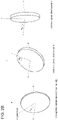
- FIG. 2b illustrates what is described supra, where a tilt about the X axis is shown as ⁇ X , where a tilt about the Y axis is shown as ⁇ Y and where a tilt about the Z axis is shown as ⁇ Z .
- two isotropic plates (P) are oriented at equal and opposite angles about the X or Y axis.
- the waveplates (Q) and the waveplate (H) are oriented normal to a plane of light propagation.
- the waveplate (Q), the waveplate (H) or the isotropic plate (P) is coated or uncoated.
- Coatings provide a way to modify the amplitude profile of the spectrum or provide attenuation of the light beam, whether applied to the waveplates or the isotropic plates.
- Preferred exemplary coatings may be dielectric or metallic coatings, and the coating may be a single layer or multi-layered.
- Waveplates are constructed out of a birefringent material, for which the index of refraction is different for different polarizations of light passing through it.
- the waveplate (Q) or the waveplate (H) comprises a birefringent material. Examples include, but are not limited to, crystalline quartz, magnesium fluoride, calcite, alpha barium borate or sapphire.
- the isotropic plate (P) comprises an isotropic material having transparency over the wavelength range of interest for the instrument being calibrated.
- examples include, but are not limited to, fused silica, fused quartz, calcium fluoride, lithium fluoride or barium fluoride.
- one or more waveplates may be replaced by a single wavelength compound zero order retarder or an achromatic retarder.
- the retarder may be any birefringent material.
- a compound zero-order quartz retarder improves performance by combining two multiple-order quartz waveplates with the desired retardance difference.
- the crystal axis of one plate is orthogonally to the crystal axis of the other, cancelling the large retardance values and leaving only the desired fractional retardance difference.
- Achromatic retarders provide a constant phase shift independent of the wavelength of light that is used (over a limited range of wavelengths). This wavelength independence is achieved by using two different birefringent crystalline materials. These devices can be used with a coherent light source, since single wavelength retarders and achromatic retarders are almost always antireflection (AR) coated and designed to be usable with lasers.
- AR antireflection
- the devices of the present invention may further comprise a neutral density (ND) filter.
- ND filter is a filter that reduces or modifies the intensity of all wavelengths of light approximately equally.
- An ND filter may be added to the devices described herein without changing the CD signal. This will allow control of the effective absorbance of the standard independently of the CD, allowing calibration measurements to be made over different gain regions of the detector.
- the ND filter may be disposed in series either before the first waveplate or after the last waveplate.
- the devices of the present invention may further comprise a mechanical light attenuator (MLA).
- MLA is a filter that reduces or modifies the intensity of all wavelengths of light approximately equally by obstructing a part of the beam.
- An MLA may be added to the devices described herein without changing the CD signal. This will allow control of the effective absorbance of the standard independently of the CD, allowing calibration measurements to be made over different gain regions of the detector.
- the MLA may be disposed at any position within the optical assembly.
- the device of the present invention may further comprise, but is not limited to, any one or more of the following:
- the devices of the present invention have many advantages, including being an out-of-the box solution, where no sample preparation is required.
- the devices are rugged and long lasting, and there are minimal degradation issues.
- the devices provide true broadband calibration, with the full relevant wavelength range covered. Very low attenuation enables calibration well into the VUV (170nm). Accuracy is completely definable from the manufacturing process and known material properties, and the devices described herein have excellent potential to become certified traceable standards.
- a first spectrum is measured, the device is rotated axially through a fixed angle and a second spectrum is measured.
- the fixed angle is 90° or 180°.
- a further step of taking the average of the two measured spectra is preferably carried out.
- a first spectrum is measured, the device is rotated axially through a fixed angle and a second spectrum is measured, the device is rotated axially through a further fixed angle and a third spectrum is measured.
- the fixed angles are 45° and 45° or 90° and 90°. The angles may be measured clockwise or anticlockwise.
- the measured spectra are processed through an algorithm to produce a resultant (corrected) spectrum.
- the spectrum may be corrected by subtracting the spectrum measured using a device according to the invention.
- the zero crossings of the measured spectrum may be used to calibrate the wavelength of the instrument.
- the device of the present invention may also allow simultaneous PEM and CD calibration, and simultaneous PEM, CD and wavelength calibration.
- One device ( L.A. Nafie, T. A. Kiederling and P.J. Stevens, "Vibrational Circular Dichroism", Jour. Am. Chem. Soc., 98(10), 2715 (1975 )) consists of a birefringent sapphire plate (a waveplate) and a linear polarizer and is designed for calibration of VCD (i.e. infra-red CD) spectrometers.
- VCD i.e. infra-red CD
- This device is limited in at least two principal ways: 1) Having an adjustable tilt angle on the isotropic plate severely limits the accuracy at which the angle of this plate can be set, in turn limiting the calibration accuracy. Indeed, it is a novel and surprising finding of the present invention that the angle of the tilted plate is critical to the CD signal produced, and needs to be fixed at a precise angle in order to provide an accurate calibration standard. 2) Like Norden and Seth (supra), it is again assumed that the waveplate is a single wavelength device, and as such the calibration standard is only applicable at a single wavelength. The authors suggest the use of a pockels cell or compensator to provide access to multiple wavelengths, again failing to realize that a standard waveplate can act as an effective ⁇ 1/4 wave device at multiple wavelengths.
- a further drawback of the devices described in the prior art is that they fail to adequately take account of the effect of beam geometry (incident angle and especially divergence) on the CD signals produced.
- Norden and Seth do examine the sensitivity of the tilt angle of the plates (which is equivalent the beam incident angle) but only with a view to minimizing this sensitivity in the construction rather than implementing methods to correct the error.
- Steinberg describes a method to align the device in the instrument, minimizing the effect of beam incident angle error. However this method is defined for a CPL instrument rather than for a CD instrument.
- the present invention incorporates an understanding of beam geometry effects and includes compensation methods, both in the device construction (e.g.
- the compound, multilayer antireflective (VAR) coated waveplate was replaced by a single uncoated low order quartz waveplate. As in previous iterations of the device, the plate was oriented with its crystal axis at 45° degrees from horizontal. The reduced reflection coefficients in the UV and red, combined with the true low-order character of the waveplate, substantially reduced the fringing effects seen previously.
- the tilted fused silica isotropic plate (isoplate) was replaced by two plates in a V configuration ('V-plates'). The purpose of this was to reduce the angular sensitivity, since a positive ray angle error on one plate would be compensated by a corresponding negative error on the other plate.
- a design based on a pair of prisms was also investigated. It was found that for optimal performance the prisms had to be set at the minimum deviation angle, which is wavelength dependent.
- a second single crystal quartz waveplate identical to the first, was positioned after the V-plates, with its crystal axis at 90° to that of the first plate.
- the purpose of this second plate was to convert linear states back into circular states, in theory eliminating the effect of detector polarisation bias on the measured signal.
- FIG. 2 A diagram of the device in this updated configuration is shown in Figure 2 .
- the basic principle of the device is as follows. At particular wavelengths (where the waveplate has a net +1 ⁇ 4 wave or -1 ⁇ 4 wave retardation), left and right circular polarised states hitting the first waveplate are converted into vertical and horizontal linear polarised states. These linear states then meet the V-plates where they are subject to linear diattentuation (or linear dichroism) due to differential Fresnel reflection from the tilted surfaces. The second waveplate converts the linear states back into circular states, so that overall the device appears to have a circular diattentuation (or circular dichroism) relative to the input state. At other wavelengths, circular states are converted to elliptical states of varying ellipticity. These in turn suffer a lower diattentuation at the V-plates.
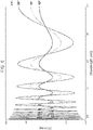
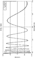
- the spectrum consists of a series of negative and positive peaks, where the peak positions are determined by the waveplate retardation, and the peak magnitudes are determined by the V-plates (isoplates) diattentuation, both of which vary with wavelength.
- This equation includes the contribution from the infinite series of rays which undergo reflections inside each isoplate. Those rays which are deflected by the plate are assumed to rapidly migrate out of the beam and hence do not contribute to the final signal as shown in Figure 3 .
- CD DichOS ⁇ sin 2 ⁇ C ⁇ sin ⁇ ⁇ ⁇ LD Vplates ⁇
- the theoretical CD spectrum of the device is computed based on the following design parameters used for a prototype configuration (which represents a physically realizable device):
- the material of the V-plates is assumed to be fused silica while that of the waveplates is assumed to be crystal quartz.
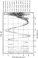
- the model of the theoretical spectrum presented herein includes consideration of ray paths having up to two internal reflections at the waveplate interfaces (higher order reflections have negligible amplitude). Accounting also for a 30% reflection from the detector surface as well (which is reasonable for a LAAPD detector) a total of six ray paths were included in the calculation in addition to the direct path which generates the main signal. The magnitude of the contribution from the reflected paths can be seen from the lighter trace in Figure 4 and Figure 5 (where the Y axis has been magnified by a factor of 1000). As shown in these Figures, the reflected contributions to the final signal are extremely small, at less than 0.3mdeg and contributing less than 0.1% of the total signal.
- ⁇ IP 20° the upper end of the dynamic range for a typical CD instrument is approached. Accordingly, the most appropriate choice of value for ⁇ IP should take account of tolerance considerations among other factors, as will be discussed infra.
- T X 4 n 2 cos 2 ⁇ IP n 2 ⁇ sin 2 ⁇ IP sin 2 ⁇ IP ⁇ n 4 cos 2 ⁇ IP ⁇ n 2 2
- T Y 4 n 2 cos 2 ⁇ IP n 2 ⁇ sin 2 ⁇ IP sin 2 ⁇ IP ⁇ cos 2 ⁇ IP ⁇ n 2 2
- M WPVP 1 2 T X + T Y + cos ⁇ ⁇ T X ⁇ T Y ⁇ sin ⁇ ⁇ T x ⁇ T y ⁇ i sin ⁇ ⁇ T x ⁇ T y ⁇ i T X + T Y - cos ⁇ ⁇ T X ⁇ T Y
- V 1 i 1 + cos ⁇ sin ⁇ 1 + cos ⁇
- ⁇ 1 T X ⁇ e i ⁇
- V 2 ⁇ i 1 ⁇ cos ⁇ sin ⁇ 1 ⁇ cos ⁇
- ⁇ 2 T Y ⁇ e i ⁇
- the dot product of V 1 and V 2 is zero, indicating that the eigenstates are orthogonal for all values of retardation ⁇ .
- the eigenvalues ⁇ 1 and ⁇ 2 indicate amplitude attenuation by T X and T Y (corresponding to irradiance attenuation by T X and T Y ) for eigenstates V 1 and V 2 .
- the factor e i ⁇ simply represents the net phase shift of the emerging beam after passing through the two crossed waveplates of retardance ⁇ . Since this phase shift applies to both eigenstates it does not change the polarisation state and can be factored out.
- the device could generally be described as behaving like a sample with elliptical dichroism (ED) for oppositely handed elliptical states with azimuths lying along X (horizontal) and Y (vertical) and wavelength dependent ellipticity varying continuously through LCP, linear and RCP states.
- ED elliptical dichroism
- the optical device described in the foregoing example is an intrinsically low absorbance standard, since the only optical losses are due to surface reflections at the various interfaces (in particular those of the V-plates). This is a useful characteristic as it allows spectra to be recorded down to very low wavelengths (approaching 170nm).
- NA neutral density filter
- MLA mechanical light attenuator
- a suitable place for an ND filter is either before the first waveplate or after the second waveplate (see Figure 2 ), since in these locations the sensitivity to the angular alignment of the filter is minimized.
- An MLA filter is not angularly sensitive and so may located at any position within the device.
- Waveplate candidates were found by conducting a thorough search in the thickness region 0.05mm to 0.25mm.
- the lower limit was set by manufacturing and fragility considerations. Thicknesses above the upper limit produced excessive peak density in the UV region.
- the search was conducted for waveplates made of crystalline quartz (SiO 2 ) and magnesium fluoride (MgF 2 ). Candidates were selected which had close peak correspondences with as many line source wavelengths as possible listed in Table 2 below. These lines were chosen because they have strong intensity and are well separated from neighbouring lines, allowing convenient selection using bandpass interference filters.
- peaks lying close to the CSA calibration wavelengths (290.5nm and 192.5nm) were also considered favourable since they would enable direct single point comparison of DichOS with CSA and ACS calibration samples.
- the lowest peak lies just above 170 nm and the highest occurs near 1600 nm, enabling calibration of the full CD measurement range (including extended range instruments).
- comparison with CSA calibration is easily achieved via interpolation of calibration points at neighboring peaks
- the material comprising the optimal waveplate (MgF 2 ) is well characterized and has excellent transmission in the VUV region (below 200 nm)
- beam errors can be problematic for the viability of the device because, being dependent on the characteristics of the instrument measuring beam, they cannot be controlled directly via tolerancing or metrology during manufacture of the DichOS standard itself. Instead, methods are preferred which either enable subtraction of these errors, or which render the device less sensitive to beam incidence angle and divergence.
- improved devices are much less sensitive to beam angular errors and divergence, and much less sensitive to detector polarization bias (as seen with photomultipliers). Exemplary preferred approaches are described infra.
- This example describes nine different DichOS variants that have been identified and analyzed; however it is to be understood that the number of DichOS variants is not limited to those described herein. As set forth in the description, any number of DichOS variants is envisioned by the present invention.
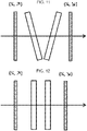
- each DichOS variant may be specified diagrammatically using the schematic symbols shown in Figure 10 , which also defines the coordinate system used.
- the viewpoint is plan (i.e. looking down from above).
- the waveplate crystal axis angle is measured anticlockwise from the positive X axis (i.e. towards Y).
- a waveplate which has a net quarter wave of retardation at the CD spectrum peak positions carries the symbol 1 ⁇ 4, while a waveplate with a net half wave of retardation at the CD peak positions carries the symbol 1 ⁇ 2. Away from the peaks the retardations will differ from these values.
- one DichOS variant can consist of a normal 1 ⁇ 4 waveplate followed by an isoplate tilted about Y, where the direction of tilt is unimportant. It thus has the classification (Q N P Y ).
- This classification scheme does not specify the crystal axis directions in the waveplates. It is assumed that the correct directions can always be inferred from the configuration, based on the required waveplate functions (convert, rotate or restore).
- the measuring beam in a CD instrument is not perfect, for example it may strike the sample at an off-normal angle and will have some divergence (i.e. not be perfectly collimated).
- the DichOS standard is sensitive to these beam imperfections.
- the principle behind this method is that the beam errors for one axial orientation are approximately equal and opposite to those for the other orientation, so the averaging method causes them to mutually cancel out.
- the correction is not perfect but in most cases reduces the beam error substantially.
- the device orientation around X and Y needs to be held stable between the two measurements.
- an associated N-plates device may be defined, which consists of the same device with all tilted surfaces replaced by normal surfaces.
- an associated N-plates corrector which we refer to as 'NCorr-6'
- the associated N-plates corrector simply has two normal isoplates between the outer waveplates (see Figure 12 ).
- the correction method using an N-plates device comprises, but is not limited only to, the following steps:
- the implementation of this method would involve either supplying the N-Corrector as a matched device with the DichOS standard, or in certain embodiments, building a slide mechanism into the DichOS device enabling the tilted plates to be switched with normal plates. In another embodiment, the plate tilt angles would be continuously adjusted against two stops. Whichever approach is used, it is important that good angular orientation (around all three axes) is maintained between the two measurements.
- the numbering system is roughly in order of increasing complexity, with the simplest device being referred to as 'DichOS-1' etc.
- the angle of the tilted isoplate surface(s) ⁇ IP was set so that all variants had approximately the same spectrum magnitude ( ⁇ 700 mdeg at 585 nm), thus ensuring a fair comparison.
- All of the DichOS variants have CD spectra similar to that shown in Figure 14 (which is actually the DichOS-6 spectrum).
- each DichOS variant does not create a new configuration.
- crystal axis angles may be interchanged in each device (45° ⁇ -45°, -45° ⁇ 45°) with the only effect being an inversion of the resulting CD spectrum. Again this interchange is not assumed to create new configurations since the resulting change in spectrum characteristic is trivial.
- DichOS-1 and DichOS-2 are of interest mainly due to their great simplicity, but are unlikely to provide suitable reference standards due to excess beam sensitivity and poor restoration of the polarization state.
- DichOS-3 suffers from beam sensitivity and unrestored polarization.
- DichOS-4 and DichOS-5 only one of these two deficits is fixed.
- the configuration which is preferred as a reference standard is DichOS-6.
- DichOS-8 and DichOS-9 are the two self-correcting configurations. Of these two, DichOS-9 may be preferable since the correction is balanced for horizontal and vertical deviations. Conditions which would favor DichOS-8 are where the beam angle or beam divergence is known to be greater in the vertical direction than horizontal, since DichOS-8 corrects vertical errors more effectively.
- the preferred embodiment is DichOS-6 with 'rotate & average' or '3-angle' correction, since this provides the best correction with minimal complexity.
- DichOS-9 represents another preferred embodiment, providing a corrected spectrum with only one measurement rather than two or three.
- one property which is not revealed in the table above is that DichOS-9, while being well corrected at the peak positions, is less well corrected than DichOS-6 at intermediate wavelengths. This can be understood by realizing that the central 1 ⁇ 2 waveplate only provides true polarization rotation at peak positions (where the polarization state after passing the front 1 ⁇ 4 waveplate is linear). If a 'rotate & average' correction is applied to DichOS-9, it is found that the errors at off-peak wavelengths clean up and the end result is similar to DichOS-6. But in this case nothing is gained over DichOS-6 at the cost of a considerable increase in device complexity.
- the 3-angle correction algorithms improve on the 'rotate & average' (R&A) method to correct for beam angle and beam divergence errors affecting the DichOS device.
- R&A 'rotate & average'
- Three versions of this algorithm (A, B and C) are described herein below. Versions A and B do not work perfectly at all wavelengths but do have the virtue of being quite simple. Version C is derived from a theoretical model of the DichOS signal for non-normal beam incidence, and thus works correctly for all wavelengths. It is, however, somewhat more complicated than versions A and B.
- CD R & A CD 0 + CD 90 2
- CD 3A CD R & A ⁇ A ⁇ C plate ⁇ sgn CD R & A
- K plate is another constant specific to the tilt angle ⁇ IP of the isotropic plates and choice of materials for the isoplates and waveplates.
- K plate 1.823518 ⁇ 10 -4 .
- K plate 2.122 ⁇ 10 -4 .
- the value of this constant may be computed for any isoplate angle and material comprising the isoplates and waveplates.
- this version of the algorithm has good correction at both the peak positions and the zero crossings for both of the preferred embodiments.
- the overcorrection at the UV end of the spectrum is somewhat worse than for version A, and at the intermediate wavelengths (between the peaks and zeroes) the error residual is undercorrected.
- This version of the algorithm does not suffer from discontinuities seen in version A.
- n ( ⁇ ) is the refractive index of the isoplates material
- n WP ( ⁇ ) is the mean refractive index of the waveplate material ( n e + n 0 )/2
- K ⁇ 180 ⁇ 10 3 2
- B ( ⁇ ) is the waveplate birefringence (n e - n o )
- ARC(A) is plotted in Figure 18 for the two preferred embodiments specified supra. This is a fixed function of wavelength for any given DichOS specification. It may be observed that the value of ARC(A) in the plateau regions is close to the values of C plate defined for version A of the algorithm (see above).
- CD 3C CD R & A ⁇ A ⁇ ARC ⁇
- Versions A and B of the algorithm are simple but do not correct perfectly at all wavelengths.
- Version C completely corrects for beam angle errors at all wavelengths. It requires computation of the ARC(A) function which is dependent on the design parameters of the DichOS-6 device.
- the ARC ( ⁇ ) function in practice could either be calculated live or stored in a table for each wavelength point between, for example, 160 nm and 2000 nm with an interval of 0.1 nm.
- the 3-angle algorithms described also correct for beam divergence errors, although not to the same degree as beam angle errors.
- the manner in which beam divergence errors are reduced by the 3-angle correction algorithms is as follows:
- the error is reduced to that corresponding to the smallest divergence with respect to azimuth. For example, if the incident beam has a 3° divergence (half-angle) in the horizontal plane and a 5° divergence in the vertical plane, 3-angle correction will reduce this to the equivalent of a 3° divergence in both horizontal and vertical.
- 3-angle correction will not reduce the residual error. For example if the beam has a divergence of 3° in both horizontal and vertical, the error remaining after 3-angle correction will be equal to that remaining after rotate & average correction.
- CD mode the measurement is in theory insensitive to the detector bias, but optical imperfections (for example strain in the PMT front window) will have the effect of making the bias response partially visible as a CD artefact.
- the DichOS device assembled according to a defined set of material and construction tolerances, preferably must meet the following performance criteria, where the accuracy figures are relative to the nominal (i.e. calculated) CD spectrum for the device: Operational wavelength range: 170nm to 1700nm CD Signal Accuracy (%) ⁇ 1% at all wavelengths Wavelength accuracy (of peak or zero crossing): ⁇ 0.05nm at 180nm ⁇ 1.0nm at 1000nm Nominal operational temperature: 20° C Allowable range of temperature variation: ⁇ 10° C
- the device must remain within specification over the temperature range given above.
- a right handed coordinate system (XYZ) is defined according to the present invention, and referred to as the 'DichOS Optical Frame' (see Figure 22 ). All of the angular orientation parameters of the DichOS optical elements are defined with reference to this frame (and hence to each other).
- the Z axis is the axis of light propagation through the device.
- an axis Z RA relative to the optical frame, representing the rotation axis of the DichOS device (as used for 'rotate & average' and '3-angle' correction methods, as described supra).
- ⁇ RA may take on any value between 0° and 360° and therefore a tolerance for this parameter is not determined, hence its exclusion from the Table.
- FIGs 23 , 24 and 25 serve to further illustrate the definitions of the various angles and angle deviations.
- the angles refer to the orientation of the crystal axis (C-axis).
- the deviations of the C-axes out of the plane of the plates are defined ( ⁇ WP 1_ C and ⁇ WP 2 _c ) which are manufacturing tolerances (of the waveplates) rather than construction tolerances. Since the waveplates are nominally oriented normal to the Z axis, the angular deviations (assumed to be small) may be treated as commutative for the purposes of the tolerance analysis.
- Figure 24 illustrates the parameters for the first waveplate. Similar definitions apply to the second waveplate.
- the Y deviations ( ⁇ ⁇ IP 1_ Y and ⁇ ⁇ IP 2 _Y ) are defined as would be expected, but the X deviations ( ⁇ ⁇ IP 1_ X and ⁇ ⁇ IP 2_ X ) are defined as being relative to the local (intrinsic) X axis, labelled X' (see Figure 25 ).
- This error therefore represents the deviation of the plate surface away from vertical. Since there is no unique axis in the isoplates, we are not concerned with Z (i.e. axial) rotations, hence only two angular parameters are required for the tolerance analysis.
- Figure 25 illustrates the parameters for the first isoplate. Similar definitions apply to the second isoplate.
- the effect of an error ⁇ B in birefringence is to cause a shift in the position of spectral peaks or zero crossings.
- ⁇ B encompasses effects due to both model errors and batch to batch material variations.
- ⁇ ⁇ ⁇ B ⁇ ⁇ ⁇ ⁇ B / ⁇ ⁇ ⁇ ⁇
- the tolerance above corresponds to 1 part in the 4 th decimal place (or least significant figure).
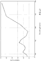
- the graph in Figure 28 shows the wavelength shift corresponding to the above thickness deviation across the whole wavelength range, for both preferred embodiments of the device specified supra., where (a) refers to the device incorporating MgF 2 waveplates and (b) refers the device incorporating quartz waveplates.
- Figure 28 shows that the shift is greater the further we move towards the IR end of the spectrum, but the error remains well below the 1nm shift at 1000nm specified in the criteria described supra for both preferred embodiments. Furthermore, the corresponding CD magnitude change is well below 0.1% at 1000nm.
- 3-angle correction should provide a useful improvement over rotate & average correction. It was decided therefore that the residual error remaining after 3-angle correction should be no greater than 25% of that remaining after rotate & average correction, which corresponds to a ⁇ CD% value of 0.05% under the conditions described above.
- quartz waveplates and MgF 2 waveplates (the production model) where nominal thickness for the quartz waveplates is 132.8 ⁇ m and for the MgF2 waveplates it is 103.7 ⁇ m. The tolerances on these thicknesses was the same for both preferred embodiments ( ⁇ 0.1 ⁇ m).
- the tolerance on the parameter ⁇ WP 2_ Z (the axial alignment of the second waveplate) is defined as an offset from an orthogonal orientation with the first waveplate. This reflects the fact that the second waveplate will be aligned to the first waveplate on a specialised jig. Any error remaining after alignment is thus correctly expressed as a relative offset rather than an absolute deviation.
- the first corresponds to a system in which the detector has no polarisation bias
- the second corresponds to a system in which the detector does have a polarisation bias response.
- the second waveplate has a more critical function within the overall device, restoring the circular polarisation state to minimise errors at the detector. This explains the change in error dependence.
- the tightest tolerances are those relating to the tilt angles of the isoplates ( ⁇ IP 1_ Y and ⁇ IP 2_ Y ) which require 1 arc minute accuracy, and the alignment of the rotation axis ( ⁇ RA ) which must coincide with the optical Z axis within 2.4 arc minutes.
- Monte-Carlo simulations were also able to take account of beam errors (divergence and incident angle errors) and detector polarisation bias. The specification of these error conditions are described herein below.
- the beam divergence values (half-angles) used in the Monte-Carlo simulations were defined as 3° in the horizontal and 3.5° in the vertical.
- the beam incidence angle was allowed to vary randomly in the vertical and horizontal directions over a range of ⁇ 2°, which is considered to represent the extremes likely to be encountered in practice:
- the beam error conditions used in the simulations are summarized in Table 8 below:
- a detector polarisation bias of ⁇ R 1% was used in the Monte-Carlo simulations. This represents the difference in response when light is linearly polarised along a preferred axis compared to the response along the orthogonal axis. Photomultipliers tend to show a polarisation sensitivity while photodiode based detectors in general do not.
- the effect of detector polarisation bias is minimized when the preferred axis is oriented at an azimuth of ⁇ 45° from the horizontal.
- a particular detector orientation on a given instrument cannot be enforced, and trying to do so would greatly complicate the use of the DichOS device as a CD standard.
- the orientation of the detector's preferred axis was allowed to vary randomly over the range 0° to 360°.
- results of the Monte-Carlo simulations are presented in the form of histograms showing the distribution with respect to percent relative CD error ( ⁇ CD% ) .
- the area under each distribution curve was normalized to unity.
- the mean value, 95% confidence interval and yield are presented in table form after each histogram plot for each of the four wavelengths tested as shown in the Figures.
- the histogram plots may be assumed to apply to both preferred embodiments of the device, as defined supra.
- the first Monte-Carlo dataset is shown in Figure 30 and serves to illustrate the effect of the construction tolerances (see Table 7) acting alone in the absence of beam errors and detector polarisation bias.
- the distribution lies comfortably within the ⁇ 1% zone.
- the mean value of ⁇ CD% is slightly negative because of the preponderance of parameters with S(-) error dependence (see Table 7).
- Dataset 2 shown in Figure 31 shows the effect of beam errors and detector polarisation bias acting together when no correction is applied.
- a significant broadening in the distribution is seen, with little change in the mean values at each wavelength. This represents worst-case conditions, with yields only in the mid 70% percent region.
- the majority of the parameters defining a DichOS device are angular construction values (see Table 6). Provided that the optical housing and mounted optical elements have no significant internal strains and can expand or contract freely without interferences being introduced, the angular parameters may be assumed to be independent of temperature. This results from the fact that isotropic linear expansions or contractions acting in three dimensions will in general be angle preserving. Hence in the analysis of the temperature dependence of the DichOS-6 device, there are only two factors which need to be considered:
- the left hand term on the right side of the equation is simply the thermal expansion coefficient of the waveplate material in the direction orthogonal to the C-axis ( ⁇ a ), which has an approximate value of 13 ⁇ 10 -6 / °C at room temperature for quartz and 8.9 ⁇ 10 -6 / °C at room temperature for magnesium fluoride.
- ( dB dT ) is the temperature coefficient of the birefringence of quartz.
- ⁇ is the wavelength in microns
- ⁇ a ⁇ 13 ⁇ 10 -6 and B( ⁇ ) is the model birefringence for quartz.
- T is the nominal temperature which here is assigned the value of 20°C.
- ⁇ T ⁇ ⁇ ⁇ ⁇ ⁇ d ⁇ d ⁇ ⁇ ⁇ T
- the wavelength shift corresponding to a temperature change of ⁇ 10°C is plotted against wavelength for one preferred embodiment (the proposed production specification) specified supra which incorporates MgF 2 waveplates.
- the shift lies in a band of approximately ⁇ 0.07nm, while at 1000nm it is within ⁇ 0.5nm.
- the shift is a little outside of specification at 180nm, but it is very likely that y has been overestimated here and that the actual shift will be lower.
- the wavelength shift is comfortably inside required ⁇ 1.0nm specification defined supra.
- the measurement is performed using at least 'rotate & average' correction, and preferably '3-angle correction'
- CD spectrometer being calibrated conforms to the instrument conditions specified in Table 8. It may also be noted that beam error and detector polarisation bias conditions utilized in this study are considered to represent the extremes of what is likely to be encountered in practice. A 'typical' system is expected to present less demanding instrument conditions.
- the device will remain within specification over a temperature range of 20°C ⁇ 10°C, where 20°C is taken to be the nominal temperature of a typical laboratory environment.
- a prototype test rig was set up which could be fitted into a sample chamber (see Figure 38 : a, b & c).
- the prototype was constructed using mounting and rotation stage components mounted onto rails which were screwed to a standard cell-block mounting platform.
- To construct the V-plates two 10° angled lens tubes were fitted into a cage-plate (for a ⁇ IP angle of 10°). Further testing was later performed on a production model of the device (see Figure 38 (d) ) built to one preferred configuration (with MgF 2 waveplates)
- the waveplates were uncoated quartz retarders specified as 2.5 waves at 532nm, and are commercially available.
- the two fusedsilica plates were 3mm thick, and are also commercially available.
- the waveplates were uncoated magnesium fluoride retarders specified as 2.25 waves at 546.1nm, and are commercially available as custom components.
- the two fused silica plates were 1mm thick and are also commercially available as custom components.
- Angular alignment of the prototype was performed, minimizing or maximising signal levels according to which element was being adjusted. This method of alignment was imperfect and better alignment is expected for the production device.
- Angular alignment of the production model was performed using a specialized jig comprising precisely aligned calcite Glan-Taylor polarizers.
- the CD instrument used for testing was carefully wavelength calibrated prior to running any tests.
- the CD scales (for PMT and LAAPD detectors) were calibrated using a freshly prepared CSA sample.
- the departure of the ⁇ IP from 10° for the prototype device can easily be explained by setup tolerances in the Thorlabs mounting components. Also this parameter would compensate for any error in the instrument CD calibration values.
- the waveplate thickness value was in excellent agreement with the measured values provided by the supplier, which were 0.1433 mm and 0.1439 mm. The thickness value above corresponds to a retardation of approximately 2.49 waves at 532 nm.
- the overlay of the measured spectrum with the calculated spectrum is shown in Figure 39(a) for the production device and Figure 39(b) for the prototype device, with a close-up of the UV region shown in Figure 40 (a and b).
- the measured spectra were recorded using an LAAPD detector and corrected for beam errors using rotate & average correction. Baselines were also measured and subtracted.
- Figure 41 shows the effect of rotating the PMT when the second waveplate is removed from the device, for the prototype device.
- the polarisation bias of the detector contributes to the overall signal, leading to a substantial variation in CD magnitude with PMT angle.
- This configuration of the device is clearly not viable as a CD standard if used with polarisation sensitive detectors such as PMTs.
- tilted plates may in be replaced with linearly dichroic samples or polarizers.
- this will in general produce signals which are too large and saturate the AC channel.
- tilted plates could be coated (either with dielectric or metal coatings) to change the magnitude characteristic of the CD spectrum.
- a metal coatings e.g. Al
- this could be used to provide attenuation (i.e. change in absorbance) in addition to changing the spectrum profile.
- tilted isoplates may be replaced by pairs of opposing wedge prisms.
- the prisms have to be paired to avoid deflecting the beam. This idea was investigated earlier in the project and found to be less effective than plates. Its only advantage is that the tilt angle is effectively held on the prism apex angle and can thus be very stable and accurately manufactured.
- the device could be augmented with neutral density filters, allowing the effective absorbance to be controlled independently.
- neutral density filters allowing the effective absorbance to be controlled independently.
- the present inventors have found that the best location for such filters is either at the front or rear of the device to reduce tilt sensitivity.
- absorptive type ND filters which cover the entire spectrum range. Reflective filters are available but earlier work suggest that the reflections can give rise to artifacts.
- An advantage of having the metal coating on a tilted surface, as mentioned above, is that the reflected beam is also deflected out of the light path.
- the device could be augmented with a mechanical light attenuator (MLA) in the form of a grid, comb, aperture or similar device which causes one portion of the beam to be interrupted while another portion of the beam is allowed to propagate.
- MLA mechanical light attenuator
- a mechanical attenuator may be disposed at any position with respect to the other optical components comprising the device and has the advantage that it is effective over the entire wavelength range and is not sensitive to tilt angle.
- the crystal axis of this waveplate can be rotated 90°. This results in either a modified CD spectrum or modified error residual.
- the crystal axis orientations defined above are the preferred ones.
- the broadband waveplates could be replaced with single wavelength zero order retarders (compound with VAR coatings) for accurate calibration at a single wavelength with minimal temperature related errors.
- the broadband waveplates could be replaced with achromatic retarders, providing in effect a flat CD spectrum over a limited wavelength range. This might be useful for example if accurate calibration was required at a set of closely spaced wavelengths over a limited spectrum range.
- axial rotation of the device could be effected by means of a motor, enabling complete automation of the calibration procedure.
- the device could be rotated continuously using a motor, in effect providing a way to mechanically average and allow the 'rotate & average' or '3-angle' corrected measurement to be obtained in a single pass rather than two.
- VUV short wavelength
- a manifold or bypass system would be employed to ensure that oxygen and other absorbing gases are purged from the spaces in between the plates.
- some form of manifold or bypass system will be employed to ensure that nitrogen can flow through the device and clear air from the spaces in between the plates.
- a means of sealing the optical housing of the device so as to enclose a nitrogen atmosphere may be employed, with a system to equalize internal and external pressure if required. In the absence of such features, the device will not function as well in the VUV region (i.e. below 200 nm)
- baffle system and/or use of absorbing paint will be used.
- beam angle errors could be corrected by angle tuning of the device while monitoring a live display of the CD signal.
- the error is minimized at the point where the CD signal is minimal.
- the angle tuning can be about a horizontal (X) axis, a vertical (Y) axis, or both.
- the CD signal could be in effect 'dialed down' to a pre-determined value. The adjustment would then be locked once the desired signal magnitude had been achieved. This would require a specially designed jig to be used during manufacture.
- the zero crossings of the CD spectrum can serve as wavelength markers, in principle allowing the device to provide a wavelength calibration in addition to CD calibration.
- the device also functions as a linear dichroism (LD) standard, where the LD peaks correspond to the zero crossings of the CD spectrum (see Figure 14 ).
- LD linear dichroism
- a preferred configuration is DichOS-6 with 'rotate & average' or '3-angle' correction to reduce the effect of beam errors.
- this involves making two measurements with the axial orientation of the device rotated 90° between the two.
- this involves making three measurements with the device rotated 45° between each measurement.
- DichOS-9 allows a corrected measurement to be obtained in a single pass. The convenience of this comes at the cost of increased complexity (and expense) of the device. DichOS-9 has good correction at all wavelengths (similar to DichOS-6) if used with rotate & average correction, but the extra complexity for no apparent performance gain does not appear to be justified.
- the devices of the present invention can be configured so as to have ⁇ 1% accuracy.
- further steps in the development of the device may be carried out, such as stray light analysis to confirm that, with a suitable blacking or trapping system, deflected rays do not reach the detector.
- the isoplates within the device have to be exceptionally clean in order to avoid generating signal artifacts, especially in the UV region of the spectrum.
- isoplates are preferably subjected to a rigorous cleaning protocol prior to being installed in the device.
- the presence of internal stress in the isoplates can introduce signal artifacts, especially in the UV part of the spectrum. As such, it is imperative to specify a high purity and low stress grade of fused silica for fabrication of the isoplates.
- the isoplates may be subjected to one or more annealing treatments in order to further reduce any residual stresses which may exist in the material.
- the DichOS peaks become narrower and as such become more susceptible to broadening and flattening as a result of convolution with the instrument line function, which typically has a bandwidth (FWHM) of 1nm.
- FWHM bandwidth
- the calculated DichOS spectrum must first be convolved with the known instrument line function at the defined measurement bandwidth (typically 1nm). This results in slightly reduced heights of the calculated peaks in the UV region. A smaller correction is required for one preferred embodiment based on MgF 2 waveplates, since the peak density in the UV is lower for this design.
Landscapes
- Physics & Mathematics (AREA)
- Health & Medical Sciences (AREA)
- Life Sciences & Earth Sciences (AREA)
- Chemical & Material Sciences (AREA)
- Analytical Chemistry (AREA)
- Biochemistry (AREA)
- General Health & Medical Sciences (AREA)
- General Physics & Mathematics (AREA)
- Immunology (AREA)
- Pathology (AREA)
- Engineering & Computer Science (AREA)
- Mathematical Physics (AREA)
- Theoretical Computer Science (AREA)
- Spectroscopy & Molecular Physics (AREA)
- Investigating Or Analysing Materials By Optical Means (AREA)
Claims (9)
- Vorrichtung zum Kalibrieren von Zirkulardichroismus- oder Lineardichroismus-Spektrometern oder von anderen auf photoelastischem Modulator basierenden Vorrichtungen oder Instrumenten, umfassend:eine erste und eine zweite Viertelwellenplatte (Q), die n ± 1/4 Wellen von Verzögerung bei einem definierten Satz von Wellenlängen bereitstellen, wobei die Viertelwellenplatten (Q) eine Dicke t aufweisen; undumfassend zwischen den zwei Viertelwellenplatten (Q) zwei identische isotrope Platten (P), die bei gleichen und entgegengesetzten Winkeln um die X- oder Y-Achse ausgerichtet sind, um eine V-Konfiguration zu bilden, wobei die Y-Achse der vertikalen Achse senkrecht zu der horizontalen Lichtausbreitungsrichtungsachse Z entspricht und die X-Achse der horizontalen Achse senkrecht zu der horizontalen Lichtausbreitungsrichtungsachse Z entspricht, wobei die zweite Viertelwellenplatte eine Kristallachse um 90° in Bezug auf die Kristallachse der ersten Viertelwellenplatte gedreht aufweist.
- Vorrichtung zum Kalibrieren von Zirkulardichroismus- oder Lineardichroismus-Spektrometern oder von anderen auf photoelastischem Modulator basierenden Vorrichtungen oder Instrumenten, umfassend:eine erste und zweite Viertelwellenplatte (Q), die n ± 1/4 Wellen von Verzögerung bei einem definierten Satz von Wellenlängen bereitstellen, wobei die Viertelwellenplatten (Q) eine Dicke t aufweisen; undumfassend zwischen der ersten und zweiten Viertelwellenplatte (Q): von der ersten Viertelwellenplatte (Q), eine erste isotrope Platte (P), die um die Y-Achse geneigt ist, wobei die Y-Achse der vertikalen Achse senkrecht zu der horizontalen Lichtausbreitungsrichtungsachse Z entspricht, gefolgt von einer Halbwellenplatte (H), die n ±1/2 Wellen von Verzögerung bei denselben Wellenlängen bereitstellt, wo die Viertelwellenplatten (Q) n ±1/4 Wellen von Verzögerung bereitstellen, wobei die Halbwellenplatte (H) eine Dicke von 2 + 4mt aufweist,wo m null oder eine positive Ganzzahl ist, gefolgt von einer zweiten isotropen Platte (P), die um die X-Achse geneigt und identisch mit der ersten isotropen Platte (P) ist,wobei die X-Achse der horizontalen Achse senkrecht zu der horizontalen Lichtausbreitungsrichtungsachse Z entspricht, wobei die zweite Viertelwellenleiterplatte dieselbe Kristallachsausrichtung wie die Kristallachse der ersten Viertelwellenplatte aufweist, jeweils eine Viertelwellennettoverzögerung bei den Wellenlängen bereitstellend, und die Halbwellenplatte eine Halbwellennettoverzögerung bei den Wellenlängen mit entgegengesetztem Vorzeichen verglichen mit der Nettoverzögerung, die von den Viertelwellenplatten bereitgestellt wird, bereitstellt.
- Vorrichtung zum Kalibrieren von Zirkulardichroismus- oder Lineardichroismus-Spektrometern oder von anderen auf photoelastischem Modulator basierenden Vorrichtungen oder Instrumenten, umfassend:eine erste und zweite Viertelwellenplatte (Q), die n ± 1/4 Wellen von Verzögerung bei einem definierten Satz von Wellenlängen bereitstellen, wobei die Wellenplatten (Q) eine Dicke t aufweisen; undumfassend zwischen der ersten und zweiten Viertelwellenplatte (Q): von der ersten Viertelwellenplatte (Q), zwei identische isotrope Platten (P), die bei gleichen und entgegengesetzten Winkeln um die Y-Achse ausgerichtet und konfiguriert sind, eine V-Konfiguration zu bilden, wobei die Y-Achse der vertikalen Achse senkrecht zu der horizontalen Lichtausbreitungsrichtungsachse Z entspricht, gefolgt von einer Halbwellenplatte (H), die n ± 1/2 Wellen von Verzögerung bei denselben Wellenlängen bereitstellt, wo die Viertelwellenplatten (Q) n ± 1/4 Wellen von Verzögerung bereitstellen, wobei die Halbwellenplatte H eine Dicke 2 + 4mt aufweist, wo m null oder eine positive Ganzzahl ist, gefolgt von zwei identischen isotropen Platten (P) senkrecht zu der Lichtausbreitungsrichtungsachse Z und identisch mit den isotropen Platten (P), die um die Y-Achse geneigt sind, wobei die zweite Viertelwellenplatte dieselbe Kristallachsenausrichtung wie die Kristallachse der ersten Viertelwellenplatte aufweist, jeweils eine Viertelwellennettoverzögerung bei den Wellenlängen bereitstellend, und die Halbwellenplatte eine Halbwellennettoverzögerung bei den Wellenlängen mit entgegengesetztem Vorzeichen verglichen mit der Nettoverzögerung, die von den Viertelwellenplatten bereitgestellt wird, bereitstellt.
- Vorrichtung zum Kalibrieren von Zirkulardichroismus- oder Lineardichroismus-Spektrometern oder von anderen auf photoelastischem Modulator basierenden Vorrichtungen oder Instrumenten, umfassend:eine erste und zweite Viertelwellenplatte (Q), die n ± 1/4 Wellen von Verzögerung bei einem definierten Satz von Wellenlängen bereitstellen, wobei die Wellenplatten (Q) eine Dicke t aufweisen; undumfassend zwischen der ersten und zweiten Viertelwellenplatte (Q): von der ersten Viertelwellenplatte (Q), zwei identische isotrope Platten (P), die bei gleichen und entgegengesetzten Winkeln um die Y-Achse ausgerichtet und konfiguriert sind, eine V-Konfiguration zu bilden, wobei die Y-Achse der vertikalen Achse senkrecht zu der horizontalen Lichtausbreitungsrichtungsachse Z entspricht, gefolgt von einer Halbwellenplatte (H), die n ± 1/2 Wellen von Verzögerung bei denselben Wellenlängen bereitstellt, wo die Viertelwellenplatten (Q) n ± 1/4 Wellen von Verzögerung bereitstellen, wobei die Halbwellenplatte (H) eine Dicke von 2 + 4mt aufweist, wo m null oder eine positive Ganzzahl ist, gefolgt von zwei identischen isotropen Platten (P), die bei gleichen und entgegengesetzten Winkeln um die X-Achse ausgerichtet sind, um eine V-Konfiguration zu bilden, und identisch mit den isotropen Platten (P) sind, die um die Y-Achse geneigt sind,wobei die X-Achse der horizontalen Achse senkrecht zu der horizontalen Lichtausbreitungsrichtungsachse Z entspricht, wobei die zweite Viertelwellenleiterplatte dieselbe Kristallachsausrichtung wie die Kristallachse der ersten Viertelwellenplatte aufweist, jeweils eine Viertelwellennettoverzögerung bei den Wellenlängen bereitstellend, und die Halbwellenplatte eine Halbwellennettoverzögerung bei den Wellenlängen mit entgegengesetztem Vorzeichen verglichen mit der Nettoverzögerung, die von den Viertelwellenplatten bereitgestellt wird, bereitstellt.
- Vorrichtung nach einem der Ansprüche 1-4, weiter umfassend eines oder mehreres des Folgenden:einen Motor, um die Vorrichtung zu rotieren oder drehen;einen Krümmer oder ein System zur Stickstoffspülung;ein Mittel zum Abdichten des optischen Gehäuses, sodass es eine Stickstoffatmosphäre umschließen kann;einen Polarisator;eine lineardichroitische Probe;einen Detektor; odereinen Prozessor.
- Verwendung der Vorrichtung nach einem der Ansprüche 1-4 zum Kalibrieren von Zirkulardichroismus- oder Lineardichroismus-Spektrometern.
- Verwendung der Vorrichtung nach einem der Ansprüche 1-4, wo ein erstes Spektrum gemessen wird, die Vorrichtung axial durch einen fixierten Winkel rotiert wird und ein zweites Spektrum gemessen wird.
- Verwendung der Vorrichtung nach Anspruch 7, wobei die Vorrichtung axial durch einen weiteren fixierten Winkel rotiert wird und ein drittes Spektrum gemessen wird.
- Verwendung der Vorrichtung nach Anspruch 7, wobei der fixierte Winkel 45°, 90° oder 180° ist.
Applications Claiming Priority (2)
| Application Number | Priority Date | Filing Date | Title |
|---|---|---|---|
| US201462060293P | 2014-10-06 | 2014-10-06 | |
| PCT/US2015/054151 WO2016057464A1 (en) | 2014-10-06 | 2015-10-06 | Calibration device and uses thereof |
Publications (3)
| Publication Number | Publication Date |
|---|---|
| EP3204754A1 EP3204754A1 (de) | 2017-08-16 |
| EP3204754A4 EP3204754A4 (de) | 2018-06-13 |
| EP3204754B1 true EP3204754B1 (de) | 2022-09-14 |
Family
ID=55653627
Family Applications (1)
| Application Number | Title | Priority Date | Filing Date |
|---|---|---|---|
| EP15848546.6A Active EP3204754B1 (de) | 2014-10-06 | 2015-10-06 | Kalibrierungsvorrichtung und verwendungen davon |
Country Status (4)
| Country | Link |
|---|---|
| US (1) | US10352846B2 (de) |
| EP (1) | EP3204754B1 (de) |
| CN (1) | CN107430063B (de) |
| WO (1) | WO2016057464A1 (de) |
Families Citing this family (3)
| Publication number | Priority date | Publication date | Assignee | Title |
|---|---|---|---|---|
| EP3414620B1 (de) * | 2016-02-10 | 2023-06-14 | Applied Photophysics Limited | Verfahren zur verbesserung der verzögerungsgenauigkeit und stabilität von photoelastischen modulatorvorrichtungen |
| RU2682605C1 (ru) * | 2017-12-27 | 2019-03-19 | Федеральное государственное бюджетное научное учреждение "Федеральный исследовательский центр "Красноярский научный центр Сибирского отделения Российской академии наук" | Устройство для калибровки дихрографов кругового дихроизма |
| EP4206651B1 (de) * | 2021-12-28 | 2026-01-28 | Tata Consultancy Services Limited | Verfahren und vorrichtung zur polarimetrischen mueller-matrix-charakterisierung transparenter objekte |
Family Cites Families (24)
| Publication number | Priority date | Publication date | Assignee | Title |
|---|---|---|---|---|
| US3637311A (en) * | 1967-10-30 | 1972-01-25 | Durrum Instr | Optical dichroism measuring apparatus and method |
| US4003663A (en) * | 1971-02-26 | 1977-01-18 | Yeda Research & Development Co., Ltd. | Device for calibrating instrument that measures circular dichroism or circularly polarized luminescence |
| US4991924A (en) * | 1989-05-19 | 1991-02-12 | Cornell Research Foundation, Inc. | Optical switches using cholesteric or chiral nematic liquid crystals and method of using same |
| US5231521A (en) * | 1989-10-30 | 1993-07-27 | The University Of Colorado Foundation, Inc. | Chiral smectic liquid crystal polarization interference filters |
| US5247176A (en) * | 1991-07-22 | 1993-09-21 | The United States Of America As Represented By The Secretary Of The Air Force | Infrared laser polarimeter |
| FR2755254B1 (fr) * | 1996-10-25 | 1999-01-15 | Centre Nat Rech Scient | Composant optique de modulation, polarimetre et ellipsometre de mueller comprenant un tel composant optique, procede de calibrage de cet ellipsometre et procede de mesure ellipsometrique |
| US6396575B1 (en) * | 2000-05-31 | 2002-05-28 | Lucent Technologies Inc. | Test and measurement system for detecting and monitoring faults and losses in passive optical networks (PONs) |
| US7218436B2 (en) * | 2003-08-08 | 2007-05-15 | General Photonics Corporation | Optical instrument and measurements using multiple tunable optical polarization rotators |
| US7079320B2 (en) * | 2003-07-15 | 2006-07-18 | Kewitsch Anthony S | Bandwidth properties of LC-SLMs for telecommunication applications with particular third compensator |
| US7233395B2 (en) * | 2003-09-25 | 2007-06-19 | Georgia Tech Research Corporation | Performing retardation measurements |
| US7233392B2 (en) * | 2004-03-25 | 2007-06-19 | Opotek, Inc. | Spectral imaging device with tunable light source |
| US7277210B2 (en) * | 2005-07-21 | 2007-10-02 | C8 Medisensors Inc. | Measuring spectral lines from an analyte using multiplexed holograms and polarization manipulation |
| CN2743859Y (zh) * | 2004-11-02 | 2005-11-30 | 曲阜师范大学激光研究所 | 低入射角敏感性的高精度消色差相位延迟器 |
| CN100426053C (zh) * | 2005-03-04 | 2008-10-15 | 上海三科仪器有限公司 | 用于紫外-近红外波段椭圆偏振光谱仪的相位补偿器 |
| US7450231B2 (en) * | 2005-11-04 | 2008-11-11 | J.A. Woollam Co., Inc. | Deviation angle self compensating substantially achromatic retarder |
| EP1957959A2 (de) * | 2005-11-30 | 2008-08-20 | Board of Trustees of Michigan State University | Identifizierung molekularer eigenschaften auf laserbasis |
| US7848020B2 (en) * | 2006-06-02 | 2010-12-07 | Jds Uniphase Corporation | Thin-film design for positive and/or negative C-plate |
| EP1892706B1 (de) * | 2006-08-23 | 2012-06-13 | JDS Uniphase Corporation | Optische Leseeinheit |
| US7796671B2 (en) * | 2008-03-31 | 2010-09-14 | Electro Scientific Industries, Inc. | Multi-pass optical power amplifier |
| DE102009015393B3 (de) * | 2009-03-20 | 2010-09-02 | Carl Zeiss Smt Ag | Messverfahren und Messsystem zur Messung der Doppelbrechung |
| CN102706539B (zh) * | 2012-06-15 | 2015-05-13 | 中国科学院上海光学精密机械研究所 | 相位延迟量分布和快轴方位角分布实时测量装置和方法 |
| US9995850B2 (en) * | 2013-06-06 | 2018-06-12 | Kla-Tencor Corporation | System, method and apparatus for polarization control |
| CN103424881B (zh) * | 2013-07-26 | 2015-06-17 | 华中科技大学 | 用于双旋转补偿器椭偏仪的菲涅尔棱镜相位延迟器 |
| CN104035204A (zh) * | 2014-06-24 | 2014-09-10 | 中国科学院光电技术研究所 | 一种偏振纯化装置 |
-
2015
- 2015-10-06 EP EP15848546.6A patent/EP3204754B1/de active Active
- 2015-10-06 WO PCT/US2015/054151 patent/WO2016057464A1/en not_active Ceased
- 2015-10-06 CN CN201580066358.7A patent/CN107430063B/zh active Active
-
2017
- 2017-03-30 US US15/474,122 patent/US10352846B2/en active Active
Also Published As
| Publication number | Publication date |
|---|---|
| CN107430063A (zh) | 2017-12-01 |
| WO2016057464A1 (en) | 2016-04-14 |
| CN107430063B (zh) | 2023-07-14 |
| US20180052098A1 (en) | 2018-02-22 |
| EP3204754A1 (de) | 2017-08-16 |
| US10352846B2 (en) | 2019-07-16 |
| EP3204754A4 (de) | 2018-06-13 |
Similar Documents
| Publication | Publication Date | Title |
|---|---|---|
| US6353477B1 (en) | Regression calibrated spectroscopic rotating compensator ellipsometer system with pseudo-achromatic retarder system | |
| Gu et al. | Optimal broadband Mueller matrix ellipsometer using multi-waveplates with flexibly oriented axes | |
| US9857292B2 (en) | Broadband and wide field angle compensator | |
| US10352846B2 (en) | Calibration device and uses thereof | |
| Johs et al. | Recent developments in spectroscopic ellipsometry for in-situ applications | |
| US6804004B1 (en) | Multiple-element lens systems and methods for uncorrelated evaluation of parameters in parameterized mathematical model equations for lens retardance, in ellipometry and polarimetry | |
| Zhang et al. | Characterization of beam splitters in the calibration of a six-channel Stokes polarimeter | |
| US8462341B2 (en) | Mounting for deviation angle self compensating substantially achromatic retarder | |
| CN103968783B (zh) | 一种测量双片波片补偿器中光轴偏差角的方法 | |
| Gu et al. | Superachromatic polarization modulator for stable and complete polarization measurement over an ultra-wide spectral range | |
| CN1856702B (zh) | 真空紫外参考反射计及其应用方法 | |
| Bian et al. | Calibration of achromatic Fresnel rhombs with an elliptical retarder model in Mueller matrix ellipsometers | |
| CN115950624B (zh) | 一种宽波段消色差相位延迟片延迟量定标系统及定标方法 | |
| Kushnir | Effect of multiple reflections of light on the optical characteristics of crystals | |
| US7215424B1 (en) | Broadband ellipsometer or polarimeter system including at least one multiple element lens | |
| Boulbry et al. | Error analysis and calibration of a spectroscopic Mueller matrix polarimeter using a short-pulse laser source | |
| Müllerová et al. | Determination of optical parameters and thickness of thin films deposited on absorbing substrates using their reflection spectra | |
| Shan et al. | Analysis of non-idealities in rhomb compensators | |
| Kaplan et al. | Infrared regular reflectance and transmittance instrumentation and standards at NIST | |
| Gong et al. | Calibration of residual polarization in light source for broadband rotating polarizer spectroscopic ellipsometer | |
| Nee | Effects of near-specular scattering on polarimetry | |
| Boulbry et al. | Development of a pulse laser-operated Mueller matrix polarimeter and implementation in the visible spectrum | |
| Vap et al. | Development of tunable polarimetric optical scattering instrument from 4.3-9.7 microns | |
| Ramanujam et al. | Quasi-achromatic rhomb compensator: Mueller matrix analysis versus azimuthal angle | |
| Kaplan et al. | Measurement of the o-ray and e-ray infrared refractive index and absorption coefficients of sapphire from 10 K to 295 K |
Legal Events
| Date | Code | Title | Description |
|---|---|---|---|
| STAA | Information on the status of an ep patent application or granted ep patent |
Free format text: STATUS: THE INTERNATIONAL PUBLICATION HAS BEEN MADE |
|
| PUAI | Public reference made under article 153(3) epc to a published international application that has entered the european phase |
Free format text: ORIGINAL CODE: 0009012 |
|
| STAA | Information on the status of an ep patent application or granted ep patent |
Free format text: STATUS: REQUEST FOR EXAMINATION WAS MADE |
|
| 17P | Request for examination filed |
Effective date: 20170504 |
|
| AK | Designated contracting states |
Kind code of ref document: A1 Designated state(s): AL AT BE BG CH CY CZ DE DK EE ES FI FR GB GR HR HU IE IS IT LI LT LU LV MC MK MT NL NO PL PT RO RS SE SI SK SM TR |
|
| AX | Request for extension of the european patent |
Extension state: BA ME |
|
| DAV | Request for validation of the european patent (deleted) | ||
| A4 | Supplementary search report drawn up and despatched |
Effective date: 20180511 |
|
| RIC1 | Information provided on ipc code assigned before grant |
Ipc: G01N 21/21 20060101ALI20180504BHEP Ipc: G01N 21/19 20060101AFI20180504BHEP |
|
| STAA | Information on the status of an ep patent application or granted ep patent |
Free format text: STATUS: EXAMINATION IS IN PROGRESS |
|
| 17Q | First examination report despatched |
Effective date: 20190430 |
|
| GRAP | Despatch of communication of intention to grant a patent |
Free format text: ORIGINAL CODE: EPIDOSNIGR1 |
|
| STAA | Information on the status of an ep patent application or granted ep patent |
Free format text: STATUS: GRANT OF PATENT IS INTENDED |
|
| INTG | Intention to grant announced |
Effective date: 20220330 |
|
| GRAS | Grant fee paid |
Free format text: ORIGINAL CODE: EPIDOSNIGR3 |
|
| GRAA | (expected) grant |
Free format text: ORIGINAL CODE: 0009210 |
|
| STAA | Information on the status of an ep patent application or granted ep patent |
Free format text: STATUS: THE PATENT HAS BEEN GRANTED |
|
| AK | Designated contracting states |
Kind code of ref document: B1 Designated state(s): AL AT BE BG CH CY CZ DE DK EE ES FI FR GB GR HR HU IE IS IT LI LT LU LV MC MK MT NL NO PL PT RO RS SE SI SK SM TR |
|
| REG | Reference to a national code |
Ref country code: GB Ref legal event code: FG4D |
|
| REG | Reference to a national code |
Ref country code: CH Ref legal event code: EP |
|
| REG | Reference to a national code |
Ref country code: DE Ref legal event code: R096 Ref document number: 602015080832 Country of ref document: DE |
|
| REG | Reference to a national code |
Ref country code: IE Ref legal event code: FG4D |
|
| REG | Reference to a national code |
Ref country code: AT Ref legal event code: REF Ref document number: 1518985 Country of ref document: AT Kind code of ref document: T Effective date: 20221015 |
|
| REG | Reference to a national code |
Ref country code: LT Ref legal event code: MG9D |
|
| REG | Reference to a national code |
Ref country code: NL Ref legal event code: MP Effective date: 20220914 |
|
| PG25 | Lapsed in a contracting state [announced via postgrant information from national office to epo] |
Ref country code: SE Free format text: LAPSE BECAUSE OF FAILURE TO SUBMIT A TRANSLATION OF THE DESCRIPTION OR TO PAY THE FEE WITHIN THE PRESCRIBED TIME-LIMIT Effective date: 20220914 Ref country code: RS Free format text: LAPSE BECAUSE OF FAILURE TO SUBMIT A TRANSLATION OF THE DESCRIPTION OR TO PAY THE FEE WITHIN THE PRESCRIBED TIME-LIMIT Effective date: 20220914 Ref country code: NO Free format text: LAPSE BECAUSE OF FAILURE TO SUBMIT A TRANSLATION OF THE DESCRIPTION OR TO PAY THE FEE WITHIN THE PRESCRIBED TIME-LIMIT Effective date: 20221214 Ref country code: LV Free format text: LAPSE BECAUSE OF FAILURE TO SUBMIT A TRANSLATION OF THE DESCRIPTION OR TO PAY THE FEE WITHIN THE PRESCRIBED TIME-LIMIT Effective date: 20220914 Ref country code: LT Free format text: LAPSE BECAUSE OF FAILURE TO SUBMIT A TRANSLATION OF THE DESCRIPTION OR TO PAY THE FEE WITHIN THE PRESCRIBED TIME-LIMIT Effective date: 20220914 Ref country code: FI Free format text: LAPSE BECAUSE OF FAILURE TO SUBMIT A TRANSLATION OF THE DESCRIPTION OR TO PAY THE FEE WITHIN THE PRESCRIBED TIME-LIMIT Effective date: 20220914 |
|
| REG | Reference to a national code |
Ref country code: AT Ref legal event code: MK05 Ref document number: 1518985 Country of ref document: AT Kind code of ref document: T Effective date: 20220914 |
|
| PG25 | Lapsed in a contracting state [announced via postgrant information from national office to epo] |
Ref country code: HR Free format text: LAPSE BECAUSE OF FAILURE TO SUBMIT A TRANSLATION OF THE DESCRIPTION OR TO PAY THE FEE WITHIN THE PRESCRIBED TIME-LIMIT Effective date: 20220914 Ref country code: GR Free format text: LAPSE BECAUSE OF FAILURE TO SUBMIT A TRANSLATION OF THE DESCRIPTION OR TO PAY THE FEE WITHIN THE PRESCRIBED TIME-LIMIT Effective date: 20221215 |
|
| PG25 | Lapsed in a contracting state [announced via postgrant information from national office to epo] |
Ref country code: SM Free format text: LAPSE BECAUSE OF FAILURE TO SUBMIT A TRANSLATION OF THE DESCRIPTION OR TO PAY THE FEE WITHIN THE PRESCRIBED TIME-LIMIT Effective date: 20220914 Ref country code: RO Free format text: LAPSE BECAUSE OF FAILURE TO SUBMIT A TRANSLATION OF THE DESCRIPTION OR TO PAY THE FEE WITHIN THE PRESCRIBED TIME-LIMIT Effective date: 20220914 Ref country code: PT Free format text: LAPSE BECAUSE OF FAILURE TO SUBMIT A TRANSLATION OF THE DESCRIPTION OR TO PAY THE FEE WITHIN THE PRESCRIBED TIME-LIMIT Effective date: 20230116 Ref country code: ES Free format text: LAPSE BECAUSE OF FAILURE TO SUBMIT A TRANSLATION OF THE DESCRIPTION OR TO PAY THE FEE WITHIN THE PRESCRIBED TIME-LIMIT Effective date: 20220914 Ref country code: CZ Free format text: LAPSE BECAUSE OF FAILURE TO SUBMIT A TRANSLATION OF THE DESCRIPTION OR TO PAY THE FEE WITHIN THE PRESCRIBED TIME-LIMIT Effective date: 20220914 Ref country code: AT Free format text: LAPSE BECAUSE OF FAILURE TO SUBMIT A TRANSLATION OF THE DESCRIPTION OR TO PAY THE FEE WITHIN THE PRESCRIBED TIME-LIMIT Effective date: 20220914 |
|
| PG25 | Lapsed in a contracting state [announced via postgrant information from national office to epo] |
Ref country code: SK Free format text: LAPSE BECAUSE OF FAILURE TO SUBMIT A TRANSLATION OF THE DESCRIPTION OR TO PAY THE FEE WITHIN THE PRESCRIBED TIME-LIMIT Effective date: 20220914 Ref country code: PL Free format text: LAPSE BECAUSE OF FAILURE TO SUBMIT A TRANSLATION OF THE DESCRIPTION OR TO PAY THE FEE WITHIN THE PRESCRIBED TIME-LIMIT Effective date: 20220914 Ref country code: IS Free format text: LAPSE BECAUSE OF FAILURE TO SUBMIT A TRANSLATION OF THE DESCRIPTION OR TO PAY THE FEE WITHIN THE PRESCRIBED TIME-LIMIT Effective date: 20230114 Ref country code: EE Free format text: LAPSE BECAUSE OF FAILURE TO SUBMIT A TRANSLATION OF THE DESCRIPTION OR TO PAY THE FEE WITHIN THE PRESCRIBED TIME-LIMIT Effective date: 20220914 |
|
| REG | Reference to a national code |
Ref country code: CH Ref legal event code: PL |
|
| REG | Reference to a national code |
Ref country code: DE Ref legal event code: R097 Ref document number: 602015080832 Country of ref document: DE |
|
| REG | Reference to a national code |
Ref country code: BE Ref legal event code: MM Effective date: 20221031 |
|
| PG25 | Lapsed in a contracting state [announced via postgrant information from national office to epo] |
Ref country code: NL Free format text: LAPSE BECAUSE OF FAILURE TO SUBMIT A TRANSLATION OF THE DESCRIPTION OR TO PAY THE FEE WITHIN THE PRESCRIBED TIME-LIMIT Effective date: 20220914 Ref country code: MC Free format text: LAPSE BECAUSE OF FAILURE TO SUBMIT A TRANSLATION OF THE DESCRIPTION OR TO PAY THE FEE WITHIN THE PRESCRIBED TIME-LIMIT Effective date: 20220914 Ref country code: LU Free format text: LAPSE BECAUSE OF NON-PAYMENT OF DUE FEES Effective date: 20221006 Ref country code: AL Free format text: LAPSE BECAUSE OF FAILURE TO SUBMIT A TRANSLATION OF THE DESCRIPTION OR TO PAY THE FEE WITHIN THE PRESCRIBED TIME-LIMIT Effective date: 20220914 |
|
| PLBE | No opposition filed within time limit |
Free format text: ORIGINAL CODE: 0009261 |
|
| STAA | Information on the status of an ep patent application or granted ep patent |
Free format text: STATUS: NO OPPOSITION FILED WITHIN TIME LIMIT |
|
| PG25 | Lapsed in a contracting state [announced via postgrant information from national office to epo] |
Ref country code: LI Free format text: LAPSE BECAUSE OF NON-PAYMENT OF DUE FEES Effective date: 20221031 Ref country code: DK Free format text: LAPSE BECAUSE OF FAILURE TO SUBMIT A TRANSLATION OF THE DESCRIPTION OR TO PAY THE FEE WITHIN THE PRESCRIBED TIME-LIMIT Effective date: 20220914 Ref country code: CH Free format text: LAPSE BECAUSE OF NON-PAYMENT OF DUE FEES Effective date: 20221031 |
|
| 26N | No opposition filed |
Effective date: 20230615 |
|
| PG25 | Lapsed in a contracting state [announced via postgrant information from national office to epo] |
Ref country code: SI Free format text: LAPSE BECAUSE OF FAILURE TO SUBMIT A TRANSLATION OF THE DESCRIPTION OR TO PAY THE FEE WITHIN THE PRESCRIBED TIME-LIMIT Effective date: 20220914 |
|
| PG25 | Lapsed in a contracting state [announced via postgrant information from national office to epo] |
Ref country code: BE Free format text: LAPSE BECAUSE OF NON-PAYMENT OF DUE FEES Effective date: 20221031 |
|
| PG25 | Lapsed in a contracting state [announced via postgrant information from national office to epo] |
Ref country code: IE Free format text: LAPSE BECAUSE OF NON-PAYMENT OF DUE FEES Effective date: 20221006 |
|
| PG25 | Lapsed in a contracting state [announced via postgrant information from national office to epo] |
Ref country code: HU Free format text: LAPSE BECAUSE OF FAILURE TO SUBMIT A TRANSLATION OF THE DESCRIPTION OR TO PAY THE FEE WITHIN THE PRESCRIBED TIME-LIMIT; INVALID AB INITIO Effective date: 20151006 |
|
| PG25 | Lapsed in a contracting state [announced via postgrant information from national office to epo] |
Ref country code: CY Free format text: LAPSE BECAUSE OF FAILURE TO SUBMIT A TRANSLATION OF THE DESCRIPTION OR TO PAY THE FEE WITHIN THE PRESCRIBED TIME-LIMIT Effective date: 20220914 |
|
| PG25 | Lapsed in a contracting state [announced via postgrant information from national office to epo] |
Ref country code: MK Free format text: LAPSE BECAUSE OF FAILURE TO SUBMIT A TRANSLATION OF THE DESCRIPTION OR TO PAY THE FEE WITHIN THE PRESCRIBED TIME-LIMIT Effective date: 20220914 Ref country code: IT Free format text: LAPSE BECAUSE OF FAILURE TO SUBMIT A TRANSLATION OF THE DESCRIPTION OR TO PAY THE FEE WITHIN THE PRESCRIBED TIME-LIMIT Effective date: 20220914 |
|
| PG25 | Lapsed in a contracting state [announced via postgrant information from national office to epo] |
Ref country code: TR Free format text: LAPSE BECAUSE OF FAILURE TO SUBMIT A TRANSLATION OF THE DESCRIPTION OR TO PAY THE FEE WITHIN THE PRESCRIBED TIME-LIMIT Effective date: 20220914 |
|
| PG25 | Lapsed in a contracting state [announced via postgrant information from national office to epo] |
Ref country code: BG Free format text: LAPSE BECAUSE OF FAILURE TO SUBMIT A TRANSLATION OF THE DESCRIPTION OR TO PAY THE FEE WITHIN THE PRESCRIBED TIME-LIMIT Effective date: 20220914 |
|
| PG25 | Lapsed in a contracting state [announced via postgrant information from national office to epo] |
Ref country code: MT Free format text: LAPSE BECAUSE OF FAILURE TO SUBMIT A TRANSLATION OF THE DESCRIPTION OR TO PAY THE FEE WITHIN THE PRESCRIBED TIME-LIMIT Effective date: 20220914 |
|
| REG | Reference to a national code |
Ref country code: GB Ref legal event code: 732E Free format text: REGISTERED BETWEEN 20251211 AND 20251217 |
|
| PGFP | Annual fee paid to national office [announced via postgrant information from national office to epo] |
Ref country code: DE Payment date: 20251013 Year of fee payment: 11 |
|
| PGFP | Annual fee paid to national office [announced via postgrant information from national office to epo] |
Ref country code: GB Payment date: 20251020 Year of fee payment: 11 |
|
| PGFP | Annual fee paid to national office [announced via postgrant information from national office to epo] |
Ref country code: FR Payment date: 20251017 Year of fee payment: 11 |