EP3200570A1 - Komponententräger mit kupfergefüllter, von laser mit mehreren durchmessern gebohrter bohrung - Google Patents
Komponententräger mit kupfergefüllter, von laser mit mehreren durchmessern gebohrter bohrung Download PDFInfo
- Publication number
- EP3200570A1 EP3200570A1 EP17153635.2A EP17153635A EP3200570A1 EP 3200570 A1 EP3200570 A1 EP 3200570A1 EP 17153635 A EP17153635 A EP 17153635A EP 3200570 A1 EP3200570 A1 EP 3200570A1
- Authority
- EP
- European Patent Office
- Prior art keywords
- bore
- component carrier
- section
- diameter
- bore section
- Prior art date
- Legal status (The legal status is an assumption and is not a legal conclusion. Google has not performed a legal analysis and makes no representation as to the accuracy of the status listed.)
- Granted
Links
Images
Classifications
-
- H—ELECTRICITY
- H05—ELECTRIC TECHNIQUES NOT OTHERWISE PROVIDED FOR
- H05K—PRINTED CIRCUITS; CASINGS OR CONSTRUCTIONAL DETAILS OF ELECTRIC APPARATUS; MANUFACTURE OF ASSEMBLAGES OF ELECTRICAL COMPONENTS
- H05K1/00—Printed circuits
- H05K1/02—Details
- H05K1/11—Printed elements for providing electric connections to or between printed circuits
- H05K1/115—Via connections; Lands around holes or via connections
-
- H—ELECTRICITY
- H05—ELECTRIC TECHNIQUES NOT OTHERWISE PROVIDED FOR
- H05K—PRINTED CIRCUITS; CASINGS OR CONSTRUCTIONAL DETAILS OF ELECTRIC APPARATUS; MANUFACTURE OF ASSEMBLAGES OF ELECTRICAL COMPONENTS
- H05K1/00—Printed circuits
- H05K1/02—Details
- H05K1/0201—Thermal arrangements, e.g. for cooling, heating or preventing overheating
- H05K1/0203—Cooling of mounted components
- H05K1/0204—Cooling of mounted components using means for thermal conduction connection in the thickness direction of the substrate
- H05K1/0206—Cooling of mounted components using means for thermal conduction connection in the thickness direction of the substrate by printed thermal vias
-
- H—ELECTRICITY
- H05—ELECTRIC TECHNIQUES NOT OTHERWISE PROVIDED FOR
- H05K—PRINTED CIRCUITS; CASINGS OR CONSTRUCTIONAL DETAILS OF ELECTRIC APPARATUS; MANUFACTURE OF ASSEMBLAGES OF ELECTRICAL COMPONENTS
- H05K1/00—Printed circuits
- H05K1/02—Details
- H05K1/09—Use of materials for the conductive, e.g. metallic pattern
-
- H—ELECTRICITY
- H05—ELECTRIC TECHNIQUES NOT OTHERWISE PROVIDED FOR
- H05K—PRINTED CIRCUITS; CASINGS OR CONSTRUCTIONAL DETAILS OF ELECTRIC APPARATUS; MANUFACTURE OF ASSEMBLAGES OF ELECTRICAL COMPONENTS
- H05K1/00—Printed circuits
- H05K1/02—Details
- H05K1/11—Printed elements for providing electric connections to or between printed circuits
- H05K1/111—Pads for surface mounting, e.g. lay-out
- H05K1/112—Pads for surface mounting, e.g. lay-out directly combined with via connections
-
- H—ELECTRICITY
- H05—ELECTRIC TECHNIQUES NOT OTHERWISE PROVIDED FOR
- H05K—PRINTED CIRCUITS; CASINGS OR CONSTRUCTIONAL DETAILS OF ELECTRIC APPARATUS; MANUFACTURE OF ASSEMBLAGES OF ELECTRICAL COMPONENTS
- H05K1/00—Printed circuits
- H05K1/18—Printed circuits structurally associated with non-printed electric components
- H05K1/181—Printed circuits structurally associated with non-printed electric components associated with surface mounted components
-
- H—ELECTRICITY
- H05—ELECTRIC TECHNIQUES NOT OTHERWISE PROVIDED FOR
- H05K—PRINTED CIRCUITS; CASINGS OR CONSTRUCTIONAL DETAILS OF ELECTRIC APPARATUS; MANUFACTURE OF ASSEMBLAGES OF ELECTRICAL COMPONENTS
- H05K3/00—Apparatus or processes for manufacturing printed circuits
- H05K3/0011—Working of insulating substrates or insulating layers
- H05K3/0017—Etching of the substrate by chemical or physical means
- H05K3/0026—Etching of the substrate by chemical or physical means by laser ablation
-
- H—ELECTRICITY
- H05—ELECTRIC TECHNIQUES NOT OTHERWISE PROVIDED FOR
- H05K—PRINTED CIRCUITS; CASINGS OR CONSTRUCTIONAL DETAILS OF ELECTRIC APPARATUS; MANUFACTURE OF ASSEMBLAGES OF ELECTRICAL COMPONENTS
- H05K3/00—Apparatus or processes for manufacturing printed circuits
- H05K3/40—Forming printed elements for providing electric connections to or between printed circuits
- H05K3/4038—Through-connections; Vertical interconnect access [VIA] connections
-
- H—ELECTRICITY
- H05—ELECTRIC TECHNIQUES NOT OTHERWISE PROVIDED FOR
- H05K—PRINTED CIRCUITS; CASINGS OR CONSTRUCTIONAL DETAILS OF ELECTRIC APPARATUS; MANUFACTURE OF ASSEMBLAGES OF ELECTRICAL COMPONENTS
- H05K3/00—Apparatus or processes for manufacturing printed circuits
- H05K3/40—Forming printed elements for providing electric connections to or between printed circuits
- H05K3/42—Plated through-holes or plated via connections
-
- H—ELECTRICITY
- H05—ELECTRIC TECHNIQUES NOT OTHERWISE PROVIDED FOR
- H05K—PRINTED CIRCUITS; CASINGS OR CONSTRUCTIONAL DETAILS OF ELECTRIC APPARATUS; MANUFACTURE OF ASSEMBLAGES OF ELECTRICAL COMPONENTS
- H05K1/00—Printed circuits
- H05K1/02—Details
- H05K1/0201—Thermal arrangements, e.g. for cooling, heating or preventing overheating
- H05K1/0203—Cooling of mounted components
- H05K1/0209—External configuration of printed circuit board adapted for heat dissipation, e.g. lay-out of conductors, coatings
-
- H—ELECTRICITY
- H05—ELECTRIC TECHNIQUES NOT OTHERWISE PROVIDED FOR
- H05K—PRINTED CIRCUITS; CASINGS OR CONSTRUCTIONAL DETAILS OF ELECTRIC APPARATUS; MANUFACTURE OF ASSEMBLAGES OF ELECTRICAL COMPONENTS
- H05K2201/00—Indexing scheme relating to printed circuits covered by H05K1/00
- H05K2201/09—Shape and layout
- H05K2201/09209—Shape and layout details of conductors
- H05K2201/095—Conductive through-holes or vias
- H05K2201/09509—Blind vias, i.e. vias having one side closed
-
- H—ELECTRICITY
- H05—ELECTRIC TECHNIQUES NOT OTHERWISE PROVIDED FOR
- H05K—PRINTED CIRCUITS; CASINGS OR CONSTRUCTIONAL DETAILS OF ELECTRIC APPARATUS; MANUFACTURE OF ASSEMBLAGES OF ELECTRICAL COMPONENTS
- H05K2201/00—Indexing scheme relating to printed circuits covered by H05K1/00
- H05K2201/09—Shape and layout
- H05K2201/09209—Shape and layout details of conductors
- H05K2201/095—Conductive through-holes or vias
- H05K2201/09563—Metal filled via
-
- H—ELECTRICITY
- H05—ELECTRIC TECHNIQUES NOT OTHERWISE PROVIDED FOR
- H05K—PRINTED CIRCUITS; CASINGS OR CONSTRUCTIONAL DETAILS OF ELECTRIC APPARATUS; MANUFACTURE OF ASSEMBLAGES OF ELECTRICAL COMPONENTS
- H05K2201/00—Indexing scheme relating to printed circuits covered by H05K1/00
- H05K2201/09—Shape and layout
- H05K2201/09209—Shape and layout details of conductors
- H05K2201/095—Conductive through-holes or vias
- H05K2201/096—Vertically aligned vias, holes or stacked vias
-
- H—ELECTRICITY
- H05—ELECTRIC TECHNIQUES NOT OTHERWISE PROVIDED FOR
- H05K—PRINTED CIRCUITS; CASINGS OR CONSTRUCTIONAL DETAILS OF ELECTRIC APPARATUS; MANUFACTURE OF ASSEMBLAGES OF ELECTRICAL COMPONENTS
- H05K2201/00—Indexing scheme relating to printed circuits covered by H05K1/00
- H05K2201/09—Shape and layout
- H05K2201/09209—Shape and layout details of conductors
- H05K2201/09654—Shape and layout details of conductors covering at least two types of conductors provided for in H05K2201/09218 - H05K2201/095
- H05K2201/09781—Dummy conductors, i.e. not used for normal transport of current; Dummy electrodes of components
-
- H—ELECTRICITY
- H05—ELECTRIC TECHNIQUES NOT OTHERWISE PROVIDED FOR
- H05K—PRINTED CIRCUITS; CASINGS OR CONSTRUCTIONAL DETAILS OF ELECTRIC APPARATUS; MANUFACTURE OF ASSEMBLAGES OF ELECTRICAL COMPONENTS
- H05K2201/00—Indexing scheme relating to printed circuits covered by H05K1/00
- H05K2201/09—Shape and layout
- H05K2201/09818—Shape or layout details not covered by a single group of H05K2201/09009 - H05K2201/09809
- H05K2201/09827—Tapered, e.g. tapered hole, via or groove
-
- H—ELECTRICITY
- H05—ELECTRIC TECHNIQUES NOT OTHERWISE PROVIDED FOR
- H05K—PRINTED CIRCUITS; CASINGS OR CONSTRUCTIONAL DETAILS OF ELECTRIC APPARATUS; MANUFACTURE OF ASSEMBLAGES OF ELECTRICAL COMPONENTS
- H05K2201/00—Indexing scheme relating to printed circuits covered by H05K1/00
- H05K2201/09—Shape and layout
- H05K2201/09818—Shape or layout details not covered by a single group of H05K2201/09009 - H05K2201/09809
- H05K2201/09854—Hole or via having special cross-section, e.g. elliptical
-
- H—ELECTRICITY
- H05—ELECTRIC TECHNIQUES NOT OTHERWISE PROVIDED FOR
- H05K—PRINTED CIRCUITS; CASINGS OR CONSTRUCTIONAL DETAILS OF ELECTRIC APPARATUS; MANUFACTURE OF ASSEMBLAGES OF ELECTRICAL COMPONENTS
- H05K2203/00—Indexing scheme relating to apparatus or processes for manufacturing printed circuits covered by H05K3/00
- H05K2203/10—Using electric, magnetic and electromagnetic fields; Using laser light
- H05K2203/107—Using laser light
-
- H—ELECTRICITY
- H05—ELECTRIC TECHNIQUES NOT OTHERWISE PROVIDED FOR
- H05K—PRINTED CIRCUITS; CASINGS OR CONSTRUCTIONAL DETAILS OF ELECTRIC APPARATUS; MANUFACTURE OF ASSEMBLAGES OF ELECTRICAL COMPONENTS
- H05K2203/00—Indexing scheme relating to apparatus or processes for manufacturing printed circuits covered by H05K3/00
- H05K2203/14—Related to the order of processing steps
- H05K2203/1476—Same or similar kind of process performed in phases, e.g. coarse patterning followed by fine patterning
-
- H—ELECTRICITY
- H05—ELECTRIC TECHNIQUES NOT OTHERWISE PROVIDED FOR
- H05K—PRINTED CIRCUITS; CASINGS OR CONSTRUCTIONAL DETAILS OF ELECTRIC APPARATUS; MANUFACTURE OF ASSEMBLAGES OF ELECTRICAL COMPONENTS
- H05K3/00—Apparatus or processes for manufacturing printed circuits
- H05K3/0011—Working of insulating substrates or insulating layers
- H05K3/0017—Etching of the substrate by chemical or physical means
- H05K3/0026—Etching of the substrate by chemical or physical means by laser ablation
- H05K3/0032—Etching of the substrate by chemical or physical means by laser ablation of organic insulating material
- H05K3/0035—Etching of the substrate by chemical or physical means by laser ablation of organic insulating material of blind holes, i.e. having a metal layer at the bottom
Definitions
- the invention relates to a component carrier, to a component carrier system and to an electronic device. Furthermore, the invention relates to a method of manufacturing a component carrier.
- PCB printed circuit boards
- component carriers comprise a plurality of bores which form vias for generating an electrical connection to an electrical component. Additional, the bores are used to provide a heat transfer in order to reduce the risk of overheating.
- Each component carrier usually comprises a plurality of vias (bores), for example more than thousand.
- Bores vias
- very small manufacturing tolerances for the size of the bores are allowed in order to provide a proper connectivity.
- the high-speed drilling process must not be only fast but must be also very accurate.
- connection pads are kept small and the bores have enough space in the component carrier.
- small sized bores also have less capacity for the heat transfer.
- a limited PCB dimension to which more and more electronic components are installed means also a higher heat spread and heat transfer requirement.
- Around 30% of bores (vias) which may be formed by laser drilling will be connected to a ground land and are dedicated for a heat spread function.
- a component carrier comprising a layer stack formed of an electrically insulating structure and an electrically conductive structure. Furthermore, the component carrier comprises a bore extending into the layer stack and having a first bore section with a first diameter and a connected second bore section with a second diameter differing from the first diameter. The component carrier further comprises a thermally conductive material filling substantially the entire bore.
- the bore may be in particular formed by laser drilling.
- component carrier may particularly denote any support structure which is capable of accommodating one or more electronic components thereon and/or therein for providing both mechanical support and electrical connectivity. Exemplary embodiments of the component carrier are described further below.
- the bore of the component carrier comprises the first bore hole section with the first diameter and the second bore hole section with the second diameter.
- the first diameter and the second diameter differ from each other.
- the first bore hole diameter is larger than the second borehole diameter.
- the first bore section and the second bore section may have a slightly conical shape.
- the first diameter may be defined by an average first diameter which is the arithmetic mean of the diameters of the first bore section, e.g. of the diameter at an opening section of the first bore section and a diameter of the first bore section which is taken at the transition of the first bore section to the transition section and/or to the second bore section.
- the second diameter may be defined by an average second diameter which is the arithmetic mean of the diameters of the second bore section, e.g.
- the first diameter may denote the opening diameter of the first bore section at the first surface and the second diameter may denote the opening diameter of the second bore section at the second surface.
- the bore is filled with the thermally conductive material.
- the thermally conductive material may also be electrically conducting.
- the thermally conductive material is copper or a copper compound.
- a multiple-diameter bore may be formed by a laser drilling process.
- the laser drilling process may be used to replace e.g. standard single diameter drill bits for mechanical drilling.
- the bore according to the present invention may be formed by varying the laser via density, the laser beam cross-sectional area and the penetration time for penetrating the layer stack with the laser radiation.
- the bore filled with the thermally conductive material may form a via as connection between two or more layers within the layer stack of the component carrier (e.g. a Printed Circuit Board).
- the via may form a through hole, a blind via or a buried via.
- a small diameter target pad size of a pad section made of the thermally conductive material and formed at an exit opening section of the bore, and additionally a better heat transfer by the thermally conductive material within the larger (second) bore section of the bore is achieved.
- the layer stack comprises a first surface and a second surface opposing the first surface, wherein the bore extends between the first surface and the second surface.
- the first bore section extends from the first surface into the layer stack and the second bore section extends from the second surface into the layer stack.
- the thermally conductive material forms a pad section onto the second surface.
- the pad section may be connected e.g. to a printed circuit board track or the like.
- the pad section is part of the thermally conductive material which fills the bore so that a via (vertical connection) through the layer stack is formed.
- the via connects other embedded components and electrically layer structures within the layer stack to the pad.
- the pad has a larger diameter than the printed circuit board track.
- the pad section has the same size (width) as the printed circuit board track.
- a pad-free connection between the printed circuit board track and the via is possible, because no production tolerances are necessary.
- a pad-free and so called “landless" (joint free) via-printed circuit board track connection may be provided.
- the thermally conductive material extends along the first surface for forming a heat radiation section.
- the heat radiation section forms a first covering area onto the first surface and the pad forms a second covering area onto the second surface.
- the first covering area is larger than the second covering area.
- an overhang of the heat radiation section which is defined between a circumference of the heat radiation section and an edge of the first bore section at the first surface is limited in size, because if the overhang exceeds a certain threshold size, the risk of voids, cracks and other plating defects during a plating proceeding, where the thermally conductive material flows into the bores, increases.
- the component carrier further comprises a further bore extending into the layer stack.
- the further bore is spaced apart from the bore, wherein the further bore extends between the first surface and the second surface.
- the thermally conductive material is filling substantially the entire further bore.
- the further bore may be formed with a uniform diameter or may be formed according to the bore with different diameter sections as described above.
- the thermally conductive material extends along the first surface between the bore and the further bore.
- a common heat radiation section for the bore and the further bore may be generated.
- the heat radiation section of the bore may be electrically isolated with respect to the further heat radiation section of the further bore.
- the first diameter merges into the second diameter.
- the first diameter is greater than the second diameter.
- the first diameter may be, just as an example, between approximately 50 ⁇ m (micrometer) to approximately 300 ⁇ m, in particular approximately 70 ⁇ m to approximately 150 ⁇ m.
- the second diameter may be, just as an example, between approximately 20 ⁇ m to approximately 100 ⁇ m, in particular approximately 40 ⁇ m to approximately 80 ⁇ m.
- the transition section may be defined as a section, where the larger diameter reduces and merges to the smaller diameter.
- the transition section length along a bore axis may be, just as an example, 1/2 to 1/15 of the total bore length and hence the total thickness of the component carrier.
- the transition section length along the bore axis may be, just as an example, 1/4 of the total bore length and hence the total thickness of the component carrier.
- the bore has a slope shape.
- the bore with the slope shape comprises for example an upper first bore section and a lower second bore section, wherein between the first bore section and the second bore section the transition section is formed.
- the first bore section comprises a larger diameter than the second bore section.
- the first bore section comprises a slightly conical shape, wherein the first diameter of the first bore section reduces from the opening section of the first bore section at the first surface along the direction to the transition section.
- the walls forming the first bore section may have a curved shape.
- the second bore section comprises a smaller diameter than the first bore section.
- the second bore section comprises a slightly conical shape, wherein the second diameter of the second bore section reduces from the transition section along the direction to the second opening section of the second bore at the second surface.
- the walls forming the second bore section may have a curved shape.
- the transition section comprises a rapidly reducing diameter along the bore axis from the first bore section in the direction to the second bore section.
- the transition section forms an S-shaped run.
- the average diameter of the transition section may be, just as an example, between approximately 15 ⁇ m (micrometer) to approximately 200 ⁇ m, in particular approximately 30 ⁇ m to approximately 100 ⁇ m.
- first bore section and the second bore section comprise a common bore axis.
- the transition section extends within a plane having a normal, wherein the transition section is formed such that an angle between the normal and the common bore axis is approximately ⁇ 35 degree and for example parallel with the common bore axis.
- the slope shape of the bore may be literally seen as an onion dome shape.
- the slope shape of the bore may be preferably formed by laser drilling, because the slope shape is formable by adapting the laser intensity and the laser line width.
- the first bore section comprises a first aspect ratio which is the ratio between a first length of the first bore section and the diameter of the first bore section at the first surface.
- the second bore section comprises a second aspect ratio which is the ratio between a second length of the second bore section and the diameter of the second bore section at the second surface. The first aspect ratio is smaller than the second aspect ratio.
- the plating capability can be improved by a reduction of aspect ratio AR.
- the aspect ratio AR can be reduced by decreasing the length of the bore and/or by increasing the opening diameter R.
- the opening diameter R of the first bore section can be increased as well in order to provide a large surface of the heat radiation section, wherein the diameter R of the second bore section is reduced in order to provide a small sized pad section along the second surface.
- first length of the first bore section may be formed larger than the second length of the second bore section in order to provide a proper aspect ratio for both, the first bore section and the second bore section.
- first length may have the double length of the second length.
- the aspect ratio for the first bore section and the second bore section is smaller than approximately 1, more in particular smaller than 0,8.
- the aspect ratios of the first bore section and the second bore section may differ with respect to each other or may be equal (in particular by adjusting the lengths and widths of both bore section with respect to each other).
- the bore according to the present invention comprises the first aspect ratio of the first bore section and the second aspect ratio of the second bore section. Hence, the sum of both aspect ratios may be smaller than the overall aspect ratio of conventional bores.
- the overall aspect ratio of the bore is reduced to ease a (copper) plating process. Furthermore, a smaller pad section of the second bore section is formed and the internal stress of the component carrier is reduced and the reliability is improved. Furthermore, it may be in general advantageous to keep the impedance within the component carrier constant. However, constant impedance between conductive parts or lines and vias of the component carrier is difficult. By a smaller diameter (e.g. by the smaller second bore section comprising the second opening diameter), the capacity will be reduced and also the land and pad-size, respectively, may be reduced. As described above, also a "landless" via may be formed. A smaller land or a landless via affects also the capacity and the impedance, respectively.
- the impedance may be regulated and adjusted, respectively, such that an impedance difference between a conductive line and a via may be compensated.
- a further advantage may be the reduction of loss. Because the diameter may be reduced, the capacity is reduced as well and thus charging currents are reduced which results in reduced charging currents, respectively.
- the bore with the slope like shape by a laser drilling method
- a laser formed via (bore) with a bigger first opening diameter of the first bore section along with a smaller connection diameter (a smaller pad section) of the second bore section can be provided.
- the bigger opening diameter allows a smaller aspect ratio AR which will be beneficial for a plating process.
- the bigger first opening diameter provides a bigger heat spread area (i.e.
- the heat radiation section which means that the amount of laser vias which are only used for heat transport may be reduced, because the required heat transfer capacity can be provided by the vias (bores) formed according to the present invention which are also used for electrical connectivity and additionally for providing a larger heat transfer capacity.
- the at least one electrically insulating (layer) structure comprises at least one of the group consisting of resin, in particular Bismaleimide-Triazine resin, cyanate ester, glass, in particular glass fibers, prepreg material, polyimide, liquid crystal polymer, epoxy-based Build-Up Film, FR4 material, a ceramic, and a metal oxide.
- resin in particular Bismaleimide-Triazine resin, cyanate ester, glass, in particular glass fibers, prepreg material, polyimide, liquid crystal polymer, epoxy-based Build-Up Film, FR4 material, a ceramic, and a metal oxide.
- prepreg or FR4 are usually preferred, other materials may be used as well.
- the at least one electrically conductive (layer) structure comprises at least one of the group consisting of copper, aluminum, and nickel. Although copper is usually preferred, other materials are possible as well.
- the component carrier is shaped as a plate. This contributes to the compact design of an electronic device, wherein the component carrier nevertheless provides a large basis for mounting electronic components thereon. Furthermore, in particular a naked die as preferred example for an embedded electronic component, can be conveniently embedded, thanks to its small thickness, into a thin plate such as a printed circuit board.
- the component carrier is configured as one of the group consisting of a printed circuit board, and a substrate.
- the term "printed circuit board” may particularly denote a plate-shaped component carrier which is formed by laminating several electrically conductive layer structures with several electrically insulating layer structures, for instance by applying pressure, if desired accompanied by the supply of thermal energy.
- the electrically conductive layer structures are made of copper
- the electrically insulating layer structures may comprise resin and/or glass fibers, so-called prepreg or FR4 material.
- the various electrically conductive layer structures may be connected to one another in a desired way by forming through-holes through the laminate, for instance by laser drilling or mechanical drilling, and by filling them with electrically conductive material (in particular copper), thereby forming vias as through-hole connections.
- a printed circuit board is usually configured for accommodating one or more electronic components on one or both opposing surfaces of the plate-shaped printed circuit board. They may be connected to the respective main surface by soldering.
- substrate may particularly denote a small component carrier having substantially the same size as an electronic component to be mounted thereon.
- the component carrier is a laminate-type component carrier.
- the component carrier is a compound of multiple layer structures which are stacked and connected together by applying a pressing force, if desired accompanied by heat.
- an electronic device comprising an electronic component with electric terminals and an above described component carrier in which the electronic component is packaged.
- the electronic component is selected from a group consisting of an active electronic component, a passive electronic component, an electronic chip, a storage device, a filter, an integrated circuit, a signal processing component, a power management component, an optoelectronic interface element, a voltage converter, a cryptographic component, a transmitter and/or receiver, an electromechanical transducer, a sensor, an actuator, a microelectromechanical system, a microprocessor, a capacitor, a resistor, an inductance, a battery, a switch, a camera, an antenna, and a logic chip.
- a magnetic element can be used as an electronic component.
- Such a magnetic element may be a permanent magnetic element (such as a ferromagnetic element, an antiferromagnetic element or a ferromagnetic element, for instance a ferrite core) or may be a paramagnetic element.
- a permanent magnetic element such as a ferromagnetic element, an antiferromagnetic element or a ferromagnetic element, for instance a ferrite core
- other electronic components in particular those who generate and emit electromagnetic radiation and/or are sensitive with regard to electromagnetic radiation propagating to the electronic component from an environment, may be embedded in the electronic device.
- a component carrier system which comprises an above described component carrier and a further above described component carrier.
- the component carrier is arranged onto the further component carrier such that the second bore section of the component carrier abuts onto the further first bore section of the further component carrier.
- the second bore section of the bore of the component carrier and the second bore section of the further bore of the further component carrier are facing one another while the first bore section of the bore of the component carrier and the first bore section of the further bore of the further component carrier are opposing one another.
- the second bore section of the bore of the component carrier and the second bore section of the further bore of the further component carrier are laterally displaced relative to one another.
- the system further comprises a high density layer structure arranged between and electrically and/or thermally coupled with the second bore section of the bore of the component carrier and the second bore section of the further bore of the further component carrier on opposing main surfaces of the high density layer structure.
- the high density layer structure is a single layer structure or a multiple layer structure.
- the electronic component is packaged in a high density layer structure of the component carrier system.
- a method of manufacturing a component carrier is described.
- a layer stack of an electrically insulating structure and an electrically conductive structure is formed.
- a bore extending into the layer stack is bored, wherein the bore has a first bore section with a first diameter and a connected second bore section with a second diameter differing from the first diameter.
- Substantially the entire bore is filled with a thermally conductive material.
- the bore is drilled by a laser drilling device.
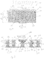
- Figure 1 illustrates a component carrier 100 into which an electrical component can be embedded or mounted thereon.
- the component carrier 100 comprises a layer stack 101 formed of an electrically insulating structure and an electrically conductive structure and a bore 110 extending into the layer stack 101 and having a first bore section 111 with a first diameter D1 and a connected second bore section 112 with a second diameter D2 differing from the first diameter D1.
- the component carrier 100 further comprises a thermally conductive material 102 filling substantially the entire bore 110.
- the bore 110 is in particular formed by laser drilling.
- the first bore hole diameter D1 is larger than the second borehole diameter D2.
- the bore 110 is filled with the thermally conductive material 102.
- the thermally conductive material 102 may also be electrically conducting.
- the thermally conductive material 102 is copper or a copper compound.
- the bore 110 filled with the thermally conductive material 102 may form a via as connection between two or more layers within the layer stack 101 of the component carrier 100.
- the first bore section 111 and the second bore section 112 may have a slightly conical shape.
- the first diameter D1 may be defined by an average first diameter D1 which is the arithmetic mean of the diameters of the first bore section 111, e.g. of the diameter at an opening section of the first bore section 111 and a diameter of the first bore section 111 which is taken at the transition of the first bore section 111 to the transition section 113 and/or to the second bore section 112.
- the second diameter D2 may be defined by an average second diameter which is the arithmetic mean of the diameters of the second bore section 112, e.g. of the diameter at an opening section of the second bore section 112 and a diameter of the second bore section 112 which is taken at the transition of the second bore section 112 to the transition section 113 and/or to the first bore section 111.
- the layer stack 101 comprises a first surface 103 and a second surface 104 opposing the first surface 103, wherein the bore 110 extends between the first surface 103 and the second surface 104.
- the first bore section 111 extends from the first surface 103 into the layer stack 101 and the second bore section 112 extends from the second surface 104 into the layer stack 101.
- the thermally conductive material 102 forms a pad section 105 onto the second surface 104.
- the pad section 105 may be connected e.g. to a printed circuit board track.
- the pad section 105 is part of the thermally conductive material 102 which fills the bore 110 so that a via (vertical connection) through the layer stack 101 is formed.
- the via connects other embedded components and electrically layer structures within the layer stack 101 to the pad section 105.
- the pad section 105 has a larger diameter than the printed circuit board track.
- the pad section 105 size may be reduced and has the same size (width) as the printed circuit board track.
- the thermally conductive material 102 extends along the first surface 103 for forming a heat radiation section 106.
- the heat radiation section 106 forms a first covering area onto the first surface 103 and the pad section 105 forms a second covering area onto the second surface 104.
- the first covering area is larger than the second covering area.
- the overhang section 301 (see Figure 3 ) of the heat radiation section 105 which is defined between a circumference of the heat radiation section 105 and an edge of the first bore section 111 at the first surface 103 is limited in size, because if the overhang section 301 exceeds a certain threshold size, the risk of voids, cracks and other plating defects during a plating proceeding, where the thermally conductive material 102 flows into the bores 110, increases.
- the diameter for calculating the aspect ratio may be the diameter of a respective opening section of respective bore sections 111, 112 or the above described average diameter of the respective bore sections 111, 112.
- the first bore section 111 comprises a larger diameter D1 than the second diameter D2 of the second bore section 112.
- the first bore section 111 comprises a slightly conical shape, wherein the first diameter D1 of the first bore section 111 reduces from the opening section of the first bore section 111 at the first surface 103 along the direction to the transition section 113.
- the circumferential area of the conical first bore section 111 may have a slightly curved shape.
- the second bore section 112 comprises a smaller diameter D2 than the first bore section 111.
- the second bore section 112 comprises a slightly conical shape, wherein the second diameter D2 of the second bore section 112 reduces from the transition section 113 along the direction to the second opening section of the second bore 112 at the second surface 104.
- the circumferential area of the conical second bore section 112 may have a slightly curved shape.
- the transition section 113 comprises a strong reducing diameter along the bore axis 108 from the first bore section 111 in the direction to the second bore section 112. In a cross-sectional view as shown in Figure 1 , the transition section forms an S-shaped run.
- first bore section 111 and the second bore section 112 comprise a common bore axis 108.
- the transition section 113 extends within a plane having a normal, wherein the transition section is formed such that an angle between the normal and the common bore axis 108 is approximately ⁇ 35 degree and for example parallel with the common bore axis 108.
- the slope shape of the bore 110 may be literally seen as an onion dome shape.
- the first bore section 111 comprises a first aspect ratio which is the ratio between the first length L1 of the first bore section 111 and the diameter D1 (opening diameter) of the first bore section 110 at the first surface 103.
- the second bore section 112 comprises a second aspect ratio which is the ratio between a second length L2 of the second bore section 112 and the diameter D2 (opening diameter) of the second bore section 112 at the second surface 104.
- the first aspect ratio may be smaller than the second aspect ratio.
- the bore 110 shown in Figure 1 is designed such that the first bore section 111 having e.g. a larger diameter D1 than the second bore section 112.
- the opening diameter R (D1) of the first bore section 111 is increased in order to provide a large surface area 301 of the heat radiation section 106, wherein the diameter R (D2) of the second bore section 112 is reduced in order to provide a small sized pad section 105 along the second surface 104.
- first length L1 of the first bore section 111 is formed larger than the second length L2 of the second bore section 112 in order to provide a proper aspect ratio AR for both, the first bore section 111 and the second bore section 112.
- first length L1 may have the double length of the second length L2.
- the first length L1 is defined as the length from the first surface 103 along the bore axis 108 to the transition section 113.
- the second length L2 is defined as the length from the second surface 104 along the bore axis 108 to the transition section 113.
- Half of the transition section length is assigned to the first length L1 and the other half of the transition section length is assigned to the second length L2.
- the bore 110 with the slope like shape as shown in Figure 1 by a laser drilling method
- a laser formed via (bore 110) with a bigger first opening diameter D1 of the first bore section 111 along with a smaller connection diameter D2 (a smaller pad section) of the second bore section 112 can be provided.
- the smaller connection diameter D2 a precise registration performance on a critical capture pad 105 can be achieved.
- the bigger opening diameter D1 of the first bore 110 allows a smaller aspect ratio AR which will be beneficial for a plating process.
- the bigger first opening diameter D1 provides a bigger heat spread area (i.e. the heat radiation section 106).
- Figure 2 shows a schematic view of a component carrier 100 having a bore 110 according to the present invention which is arranged onto a further component carrier 200.
- reference numerals 100 and 110 in Figure 2 may denote two layers of one and the same board.
- the component carrier 100 comprises the bore 110 as shown in Figure 1 .
- the component carrier 100 comprises a layer stack 101 formed of an electrically insulating structure and an electrically conductive structure and a bore 110 extending into the layer stack 101 and having a first bore section 111 with a first diameter D1 and a connected second bore section 112 with a second diameter D2 differing from the first diameter D1.
- the component carrier further comprises a thermally conductive material 102 filling substantially the entire bore 110.
- the bore 110 is in particular formed by laser drilling.
- the first bore hole diameter D1 is larger than the second borehole diameter D2.
- the first bore section comprises a large heat radiation section 106, so that heat 107 is transferred away from the component carrier 100.
- the component carrier 100 comprises further bores 120 which are arranged adjacent to the bore 110.
- the further bores 120 are shown in a conventional uniform or slightly conical design.
- the further pad sections 121 of the further bores 120 and the further heat radiation sections 122 of the further bores 120 comprise almost a similar sized area, because due to the large opening diameters of the further bores 120 smaller further pad sections 121 are not possible.
- larger further heat radiation sections 122 are also not easy to manufacture due to plating process requirements.
- the component carrier 100 is arranged onto a further component carrier 200.
- the further component carrier 200 comprises further bores 210 which are filled with a thermally and electrically conductive material.
- the further bores 210 may be drilled by a laser drilling or mechanical drilling method.
- the further bores 210 comprise a further heat radiation section 206 onto which the pad section 105, 121 of the respective bores 110, 120 of the component carrier 100 are arranged and in electrical and thermal contact, respectively.
- the further heat radiation section 206 is formed along a further first surface 203 of the further layer stack 201.
- the further heat radiation section 206 may comprise thermally conductive material connecting two adjacent further bores 210.
- the further bores 210 may comprise respective further pad sections 205 which are formed along a further second surface of the further layer stack 201.
- the further pad sections 205 are in contact with a contact layer 207 which is arranged onto the further layer stack 201.
- the further bores 210 of the further component carrier 200 comprise a uniform or conical shape, so that the further heat radiation section 206 and the further pad section 205 have almost the same size.
- the further heat radiation section 206 of the further component carrier 200 comprise almost the same size as the further pad section 121 of the further bore 120 of the component carrier 100.
- mis-registration 208 which is a pad section shift of the further pad section 121 and the respective further heat radiation section 206 of the further bore 210 of the further component carrier 200.
- the mis-registration 208 describes a shift of the further bore 120 of the component carrier 100 with respect to the further bore 210 of the further component carrier 200, such that the thermally conductive material within the further bore 120 forms an overhang with respect to the thermally conductive material within the further bore 210 of the further component carrier 200.
- the mentioned overhang of the mis-registration 108 is highlighted within the circle drawn in Figure 2 .
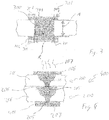
- FIG. 3 shows a schematic view of a bore for describing the definition of the aspect ratio AR.
- the plating capability can be improved by a reduction of aspect ratio AR.
- the aspect ratio AR can be reduced by decreasing the length of the bore 300 and/or by increasing the opening diameter R.
- the mentioned values of the thickness relate to a printed circuit board as component carrier. A skilled person will recognize that smaller thickness values are appropriate for a substrate as component carrier.
- an overhang 301 of the heat radiation section 303 which is defined between a circumference of the heat radiation section 303 and an edge of the bore section at the first surface is limited in size, because if the overhang 301 exceeds a certain threshold size, the risk of voids, cracks and other plating defects during a plating proceeding, where the thermally conductive material flows into the bores, increases.
- connection section 302 (pad section) which is defined between a circumference of the connection section 302 and an edge of the bore section at the first surface is limited in size.
- Figure 4 shows a schematic view of a component carrier system 400 according to an exemplary embodiment of the present invention.
- the component carrier system 400 comprises an above described component carrier 100 and a further above described component carrier 200.
- reference numerals 100 and 200 in Figure 4 may denote two layers of one and the same board.
- the component carrier 100 is arranged onto the further component carrier 200 such that the second bore section 112 of the component carrier 100 abuts onto the further first bore section of the further component carrier 200.
- the pad section 105 abuts onto the further heat radiation section 206 of the further bore 210.
- both, the bore 110 of the component carrier 100 and the further bore 210 of the further component carrier 200 are formed similar to the bore 110 is shown in Figure 1 .
- the bores 110, 210 have larger heat radiation sections 106, 206 in comparison to their respective pad sections 105, 205. Hence, proper plating characteristics are given and the risk of mis-registration is reduced.
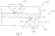
- Figure 5 shows a schematic view of a further component carrier system 400 according to an exemplary embodiment of the present invention.
- the component carrier system 400 comprises an above described component carrier 100 and a further above described component carrier 200.
- reference numerals 100 and 200 in Figure 5 may denote two layers of one and the same board.
- a high density layer 501 is arranged between the component carrier 100 and the further component carrier 200.
- the second bore section 112 of the bore 110 abuts on the first surface of the high-density layer 501 and the second bore section 112 of the further bore 210 abuts on a second surface of the high-density layer 501, wherein the first surface is an opposite side with respect to the second surface of the high-density layer 501.
- the high-density layer 501 is arranged between the second bore section 112 of the bore 110 and the second bore section of the further bore 210.
- a first pad section 105 of the bore 110 abuts on the first surface of the high-density layer 501 and a further pad section 205 of the further board 2010 abuts on the second surface of the high-density layer 501.
- the second bore section 112 of the bore 110 of the component carrier 100 and the second bore section 112 of the further bore 210 of the further component carrier 200 are facing one another while the first bore section 111 of the bore 110 of the component carrier 100 and the first bore section 111 of the further bore 210 of the further component carrier 200 are opposing one another.
- the second bore section 112 of the bore 110 of the component carrier 100 and the second bore section 112 of the further bore 210 of the further component carrier 200 are laterally displaced relative to one another.
Landscapes
- Engineering & Computer Science (AREA)
- Microelectronics & Electronic Packaging (AREA)
- Manufacturing & Machinery (AREA)
- Physics & Mathematics (AREA)
- Optics & Photonics (AREA)
- Cooling Or The Like Of Semiconductors Or Solid State Devices (AREA)
- Production Of Multi-Layered Print Wiring Board (AREA)
- Structure Of Printed Boards (AREA)
Applications Claiming Priority (1)
| Application Number | Priority Date | Filing Date | Title |
|---|---|---|---|
| CN201610066877.XA CN107027238B (zh) | 2016-01-29 | 2016-01-29 | 包括铜填充多径激光钻孔的元件载体 |
Publications (2)
| Publication Number | Publication Date |
|---|---|
| EP3200570A1 true EP3200570A1 (de) | 2017-08-02 |
| EP3200570B1 EP3200570B1 (de) | 2025-01-22 |
Family
ID=57956113
Family Applications (1)
| Application Number | Title | Priority Date | Filing Date |
|---|---|---|---|
| EP17153635.2A Active EP3200570B1 (de) | 2016-01-29 | 2017-01-27 | Komponententräger mit kupfergefüllter, von laser mit mehreren durchmessern gebohrter bohrung |
Country Status (3)
| Country | Link |
|---|---|
| US (2) | US10278280B2 (de) |
| EP (1) | EP3200570B1 (de) |
| CN (1) | CN107027238B (de) |
Cited By (1)
| Publication number | Priority date | Publication date | Assignee | Title |
|---|---|---|---|---|
| WO2020200824A1 (de) * | 2019-04-04 | 2020-10-08 | Osram Opto Semiconductors Gmbh | Träger mit verkleinerter durchkontaktierung |
Families Citing this family (4)
| Publication number | Priority date | Publication date | Assignee | Title |
|---|---|---|---|---|
| CN111508893B (zh) * | 2019-01-31 | 2023-12-15 | 奥特斯(中国)有限公司 | 部件承载件及制造部件承载件的方法 |
| CN110996513B (zh) * | 2019-10-31 | 2021-02-02 | 苏州浪潮智能科技有限公司 | 一种设计pcb焊盘的方法、设备及介质 |
| EP4091193A4 (de) | 2020-01-17 | 2024-03-20 | Kemet Electronics Corporation | Komponentenanordnungen und einbetten für elektronik mit hoher dichte |
| EP4100975A4 (de) | 2020-02-03 | 2024-08-07 | Kemet Electronics Corporation | Struktureller leiterrahmen |
Citations (2)
| Publication number | Priority date | Publication date | Assignee | Title |
|---|---|---|---|---|
| US20110148545A1 (en) * | 2009-12-18 | 2011-06-23 | Choudhury Dobabani | Apparatus and method for embedding components in small-form-factor, system-on-packages |
| US20130146349A1 (en) * | 2011-12-07 | 2013-06-13 | Samsung Electro-Mechanics Co., Ltd | Printed circuit board and method for manufacturing the same |
Family Cites Families (10)
| Publication number | Priority date | Publication date | Assignee | Title |
|---|---|---|---|---|
| US6005198A (en) | 1997-10-07 | 1999-12-21 | Dimensional Circuits Corporation | Wiring board constructions and methods of making same |
| JPH11145581A (ja) * | 1997-11-10 | 1999-05-28 | Hitachi Seiko Ltd | プリント基板の穴明け方法および装置 |
| US6373717B1 (en) * | 1999-07-02 | 2002-04-16 | International Business Machines Corporation | Electronic package with high density interconnect layer |
| JPWO2009107346A1 (ja) | 2008-02-29 | 2011-06-30 | 住友ベークライト株式会社 | 回路板および回路板の製造方法 |
| US8413324B2 (en) * | 2009-06-09 | 2013-04-09 | Ibiden Co., Ltd. | Method of manufacturing double-sided circuit board |
| US8925192B2 (en) | 2009-06-09 | 2015-01-06 | Ibiden Co., Ltd. | Printed wiring board and method for manufacturing the same |
| CN102726127A (zh) | 2010-02-05 | 2012-10-10 | 株式会社藤仓 | 配线板及其制造方法 |
| US8759691B2 (en) | 2010-07-09 | 2014-06-24 | Ibiden Co., Ltd. | Wiring board and method for manufacturing the same |
| JP5846185B2 (ja) * | 2013-11-21 | 2016-01-20 | 大日本印刷株式会社 | 貫通電極基板及び貫通電極基板を用いた半導体装置 |
| CN205793596U (zh) * | 2016-01-29 | 2016-12-07 | 奥特斯(中国)有限公司 | 元件载体和电子装置 |
-
2016
- 2016-01-29 CN CN201610066877.XA patent/CN107027238B/zh active Active
-
2017
- 2017-01-27 EP EP17153635.2A patent/EP3200570B1/de active Active
- 2017-01-28 US US15/418,711 patent/US10278280B2/en active Active
-
2019
- 2019-03-19 US US16/358,360 patent/US10701793B2/en active Active
Patent Citations (2)
| Publication number | Priority date | Publication date | Assignee | Title |
|---|---|---|---|---|
| US20110148545A1 (en) * | 2009-12-18 | 2011-06-23 | Choudhury Dobabani | Apparatus and method for embedding components in small-form-factor, system-on-packages |
| US20130146349A1 (en) * | 2011-12-07 | 2013-06-13 | Samsung Electro-Mechanics Co., Ltd | Printed circuit board and method for manufacturing the same |
Cited By (1)
| Publication number | Priority date | Publication date | Assignee | Title |
|---|---|---|---|---|
| WO2020200824A1 (de) * | 2019-04-04 | 2020-10-08 | Osram Opto Semiconductors Gmbh | Träger mit verkleinerter durchkontaktierung |
Also Published As
| Publication number | Publication date |
|---|---|
| US10701793B2 (en) | 2020-06-30 |
| US10278280B2 (en) | 2019-04-30 |
| CN107027238B (zh) | 2020-08-18 |
| US20170223820A1 (en) | 2017-08-03 |
| CN107027238A (zh) | 2017-08-08 |
| US20190215950A1 (en) | 2019-07-11 |
| EP3200570B1 (de) | 2025-01-22 |
Similar Documents
| Publication | Publication Date | Title |
|---|---|---|
| US11810844B2 (en) | Component carrier and method of manufacturing the same | |
| US10701793B2 (en) | Component carrier comprising a copper filled multiple-diameter laser drilled bore | |
| US12075561B2 (en) | Embedding component in component carrier by component fixation structure | |
| EP3582593B1 (de) | Verfahren zur herstellung eines komponententrägers mit gestufter kavität und in der gestuften kavität eingebettete, gestufte komponentenanordnung | |
| US9414497B2 (en) | Semiconductor package including an embedded circuit component within a support structure of the package | |
| CN112584611B (zh) | 具有延伸穿过多个介电层的通孔的部件承载件 | |
| US10531577B1 (en) | Forming through holes through exposed dielectric material of component carrier | |
| US11700690B2 (en) | Component carrier with blind hole filled with an electrically conductive medium and fulfilling a minimum thickness design rule | |
| US10440835B1 (en) | Forming through holes through exposed dielectric material of component carrier | |
| CN111508893B (zh) | 部件承载件及制造部件承载件的方法 | |
| TWM599067U (zh) | 具有前和後側窗口大小不同的通孔的低懸伸部件承載件 | |
| EP3425667B1 (de) | Herstellung eines halbleiterpaketes mit einer eingebetteten schaltungskomponente in einer tragestruktur des pakets und zugehörige vorrichtung | |
| CN108463047A (zh) | 基部结构上的限定腔体和对准标记的图案化覆盖层 | |
| US10433415B2 (en) | Component carrier comprising a copper filled mechanical drilled multiple-diameter bore | |
| US11410965B2 (en) | Electronic device with embedded component carrier | |
| EP3911132B1 (de) | Bauteilträger mit einem festen körper, der ein bauteilträgerloch vor dem eindringen von fremdkörpern schützt | |
| CN111511104A (zh) | 通孔中有桥结构、利用可靠性增强参数组合的部件承载件 | |
| US20250016929A1 (en) | Substrate with embedded conductive coin | |
| US12219701B2 (en) | Component carrier | |
| WO2025011781A1 (en) | Substrate with embedded conductive coin |
Legal Events
| Date | Code | Title | Description |
|---|---|---|---|
| PUAI | Public reference made under article 153(3) epc to a published international application that has entered the european phase |
Free format text: ORIGINAL CODE: 0009012 |
|
| STAA | Information on the status of an ep patent application or granted ep patent |
Free format text: STATUS: THE APPLICATION HAS BEEN PUBLISHED |
|
| AK | Designated contracting states |
Kind code of ref document: A1 Designated state(s): AL AT BE BG CH CY CZ DE DK EE ES FI FR GB GR HR HU IE IS IT LI LT LU LV MC MK MT NL NO PL PT RO RS SE SI SK SM TR |
|
| AX | Request for extension of the european patent |
Extension state: BA ME |
|
| STAA | Information on the status of an ep patent application or granted ep patent |
Free format text: STATUS: REQUEST FOR EXAMINATION WAS MADE |
|
| 17P | Request for examination filed |
Effective date: 20180122 |
|
| RBV | Designated contracting states (corrected) |
Designated state(s): AL AT BE BG CH CY CZ DE DK EE ES FI FR GB GR HR HU IE IS IT LI LT LU LV MC MK MT NL NO PL PT RO RS SE SI SK SM TR |
|
| STAA | Information on the status of an ep patent application or granted ep patent |
Free format text: STATUS: EXAMINATION IS IN PROGRESS |
|
| 17Q | First examination report despatched |
Effective date: 20200429 |
|
| GRAP | Despatch of communication of intention to grant a patent |
Free format text: ORIGINAL CODE: EPIDOSNIGR1 |
|
| STAA | Information on the status of an ep patent application or granted ep patent |
Free format text: STATUS: GRANT OF PATENT IS INTENDED |
|
| RIC1 | Information provided on ipc code assigned before grant |
Ipc: H05K 3/00 20060101ALN20241011BHEP Ipc: H05K 1/11 20060101ALI20241011BHEP Ipc: H05K 1/02 20060101AFI20241011BHEP |
|
| INTG | Intention to grant announced |
Effective date: 20241025 |
|
| RIN1 | Information on inventor provided before grant (corrected) |
Inventor name: TAMM, WILHELM Inventor name: DOU, YUCUN Inventor name: CHEN, ZHAOJIAN Inventor name: BAUER-OEPPINGER, NIKOLAUS |
|
| GRAS | Grant fee paid |
Free format text: ORIGINAL CODE: EPIDOSNIGR3 |
|
| GRAA | (expected) grant |
Free format text: ORIGINAL CODE: 0009210 |
|
| STAA | Information on the status of an ep patent application or granted ep patent |
Free format text: STATUS: THE PATENT HAS BEEN GRANTED |
|
| AK | Designated contracting states |
Kind code of ref document: B1 Designated state(s): AL AT BE BG CH CY CZ DE DK EE ES FI FR GB GR HR HU IE IS IT LI LT LU LV MC MK MT NL NO PL PT RO RS SE SI SK SM TR |
|
| REG | Reference to a national code |
Ref country code: GB Ref legal event code: FG4D |
|
| REG | Reference to a national code |
Ref country code: CH Ref legal event code: EP |
|
| REG | Reference to a national code |
Ref country code: IE Ref legal event code: FG4D |
|
| REG | Reference to a national code |
Ref country code: DE Ref legal event code: R096 Ref document number: 602017087410 Country of ref document: DE |
|
| P01 | Opt-out of the competence of the unified patent court (upc) registered |
Free format text: CASE NUMBER: APP_9173/2025 Effective date: 20250224 |
|
| REG | Reference to a national code |
Ref country code: NL Ref legal event code: MP Effective date: 20250122 |
|
| PG25 | Lapsed in a contracting state [announced via postgrant information from national office to epo] |
Ref country code: NL Free format text: LAPSE BECAUSE OF FAILURE TO SUBMIT A TRANSLATION OF THE DESCRIPTION OR TO PAY THE FEE WITHIN THE PRESCRIBED TIME-LIMIT Effective date: 20250122 |
|
| PG25 | Lapsed in a contracting state [announced via postgrant information from national office to epo] |
Ref country code: RS Free format text: LAPSE BECAUSE OF FAILURE TO SUBMIT A TRANSLATION OF THE DESCRIPTION OR TO PAY THE FEE WITHIN THE PRESCRIBED TIME-LIMIT Effective date: 20250422 |
|
| PG25 | Lapsed in a contracting state [announced via postgrant information from national office to epo] |
Ref country code: FI Free format text: LAPSE BECAUSE OF FAILURE TO SUBMIT A TRANSLATION OF THE DESCRIPTION OR TO PAY THE FEE WITHIN THE PRESCRIBED TIME-LIMIT Effective date: 20250122 |
|
| PG25 | Lapsed in a contracting state [announced via postgrant information from national office to epo] |
Ref country code: PL Free format text: LAPSE BECAUSE OF FAILURE TO SUBMIT A TRANSLATION OF THE DESCRIPTION OR TO PAY THE FEE WITHIN THE PRESCRIBED TIME-LIMIT Effective date: 20250122 |
|
| PG25 | Lapsed in a contracting state [announced via postgrant information from national office to epo] |
Ref country code: ES Free format text: LAPSE BECAUSE OF FAILURE TO SUBMIT A TRANSLATION OF THE DESCRIPTION OR TO PAY THE FEE WITHIN THE PRESCRIBED TIME-LIMIT Effective date: 20250122 |
|
| REG | Reference to a national code |
Ref country code: LT Ref legal event code: MG9D |
|
| PG25 | Lapsed in a contracting state [announced via postgrant information from national office to epo] |
Ref country code: IS Free format text: LAPSE BECAUSE OF FAILURE TO SUBMIT A TRANSLATION OF THE DESCRIPTION OR TO PAY THE FEE WITHIN THE PRESCRIBED TIME-LIMIT Effective date: 20250522 Ref country code: NO Free format text: LAPSE BECAUSE OF FAILURE TO SUBMIT A TRANSLATION OF THE DESCRIPTION OR TO PAY THE FEE WITHIN THE PRESCRIBED TIME-LIMIT Effective date: 20250422 |
|
| REG | Reference to a national code |
Ref country code: AT Ref legal event code: MK05 Ref document number: 1762456 Country of ref document: AT Kind code of ref document: T Effective date: 20250122 |
|
| PG25 | Lapsed in a contracting state [announced via postgrant information from national office to epo] |
Ref country code: HR Free format text: LAPSE BECAUSE OF FAILURE TO SUBMIT A TRANSLATION OF THE DESCRIPTION OR TO PAY THE FEE WITHIN THE PRESCRIBED TIME-LIMIT Effective date: 20250122 |
|
| PG25 | Lapsed in a contracting state [announced via postgrant information from national office to epo] |
Ref country code: LV Free format text: LAPSE BECAUSE OF FAILURE TO SUBMIT A TRANSLATION OF THE DESCRIPTION OR TO PAY THE FEE WITHIN THE PRESCRIBED TIME-LIMIT Effective date: 20250122 Ref country code: PT Free format text: LAPSE BECAUSE OF FAILURE TO SUBMIT A TRANSLATION OF THE DESCRIPTION OR TO PAY THE FEE WITHIN THE PRESCRIBED TIME-LIMIT Effective date: 20250522 |
|
| PG25 | Lapsed in a contracting state [announced via postgrant information from national office to epo] |
Ref country code: GR Free format text: LAPSE BECAUSE OF FAILURE TO SUBMIT A TRANSLATION OF THE DESCRIPTION OR TO PAY THE FEE WITHIN THE PRESCRIBED TIME-LIMIT Effective date: 20250423 Ref country code: BG Free format text: LAPSE BECAUSE OF FAILURE TO SUBMIT A TRANSLATION OF THE DESCRIPTION OR TO PAY THE FEE WITHIN THE PRESCRIBED TIME-LIMIT Effective date: 20250122 |
|
| PG25 | Lapsed in a contracting state [announced via postgrant information from national office to epo] |
Ref country code: AT Free format text: LAPSE BECAUSE OF FAILURE TO SUBMIT A TRANSLATION OF THE DESCRIPTION OR TO PAY THE FEE WITHIN THE PRESCRIBED TIME-LIMIT Effective date: 20250122 |
|
| REG | Reference to a national code |
Ref country code: CH Ref legal event code: PL |
|
| PG25 | Lapsed in a contracting state [announced via postgrant information from national office to epo] |
Ref country code: SE Free format text: LAPSE BECAUSE OF FAILURE TO SUBMIT A TRANSLATION OF THE DESCRIPTION OR TO PAY THE FEE WITHIN THE PRESCRIBED TIME-LIMIT Effective date: 20250122 |
|
| PG25 | Lapsed in a contracting state [announced via postgrant information from national office to epo] |
Ref country code: LU Free format text: LAPSE BECAUSE OF NON-PAYMENT OF DUE FEES Effective date: 20250127 |
|
| PG25 | Lapsed in a contracting state [announced via postgrant information from national office to epo] |
Ref country code: SM Free format text: LAPSE BECAUSE OF FAILURE TO SUBMIT A TRANSLATION OF THE DESCRIPTION OR TO PAY THE FEE WITHIN THE PRESCRIBED TIME-LIMIT Effective date: 20250122 |
|
| PG25 | Lapsed in a contracting state [announced via postgrant information from national office to epo] |
Ref country code: DK Free format text: LAPSE BECAUSE OF FAILURE TO SUBMIT A TRANSLATION OF THE DESCRIPTION OR TO PAY THE FEE WITHIN THE PRESCRIBED TIME-LIMIT Effective date: 20250122 |
|
| PG25 | Lapsed in a contracting state [announced via postgrant information from national office to epo] |
Ref country code: MC Free format text: LAPSE BECAUSE OF FAILURE TO SUBMIT A TRANSLATION OF THE DESCRIPTION OR TO PAY THE FEE WITHIN THE PRESCRIBED TIME-LIMIT Effective date: 20250122 |
|
| PG25 | Lapsed in a contracting state [announced via postgrant information from national office to epo] |
Ref country code: IT Free format text: LAPSE BECAUSE OF FAILURE TO SUBMIT A TRANSLATION OF THE DESCRIPTION OR TO PAY THE FEE WITHIN THE PRESCRIBED TIME-LIMIT Effective date: 20250122 |
|
| PG25 | Lapsed in a contracting state [announced via postgrant information from national office to epo] |
Ref country code: BE Free format text: LAPSE BECAUSE OF NON-PAYMENT OF DUE FEES Effective date: 20250131 |
|
| PG25 | Lapsed in a contracting state [announced via postgrant information from national office to epo] |
Ref country code: CH Free format text: LAPSE BECAUSE OF NON-PAYMENT OF DUE FEES Effective date: 20250131 |
|
| PG25 | Lapsed in a contracting state [announced via postgrant information from national office to epo] |
Ref country code: EE Free format text: LAPSE BECAUSE OF FAILURE TO SUBMIT A TRANSLATION OF THE DESCRIPTION OR TO PAY THE FEE WITHIN THE PRESCRIBED TIME-LIMIT Effective date: 20250122 Ref country code: CZ Free format text: LAPSE BECAUSE OF FAILURE TO SUBMIT A TRANSLATION OF THE DESCRIPTION OR TO PAY THE FEE WITHIN THE PRESCRIBED TIME-LIMIT Effective date: 20250122 |
|
| REG | Reference to a national code |
Ref country code: BE Ref legal event code: MM Effective date: 20250131 Ref country code: DE Ref legal event code: R097 Ref document number: 602017087410 Country of ref document: DE |
|
| PG25 | Lapsed in a contracting state [announced via postgrant information from national office to epo] |
Ref country code: RO Free format text: LAPSE BECAUSE OF FAILURE TO SUBMIT A TRANSLATION OF THE DESCRIPTION OR TO PAY THE FEE WITHIN THE PRESCRIBED TIME-LIMIT Effective date: 20250122 |
|
| PG25 | Lapsed in a contracting state [announced via postgrant information from national office to epo] |
Ref country code: SK Free format text: LAPSE BECAUSE OF FAILURE TO SUBMIT A TRANSLATION OF THE DESCRIPTION OR TO PAY THE FEE WITHIN THE PRESCRIBED TIME-LIMIT Effective date: 20250122 |
|
| PLBE | No opposition filed within time limit |
Free format text: ORIGINAL CODE: 0009261 |
|
| STAA | Information on the status of an ep patent application or granted ep patent |
Free format text: STATUS: NO OPPOSITION FILED WITHIN TIME LIMIT |
|
| GBPC | Gb: european patent ceased through non-payment of renewal fee |
Effective date: 20250422 |
|
| 26N | No opposition filed |
Effective date: 20251023 |
|
| PG25 | Lapsed in a contracting state [announced via postgrant information from national office to epo] |
Ref country code: GB Free format text: LAPSE BECAUSE OF NON-PAYMENT OF DUE FEES Effective date: 20250422 |
|
| PG25 | Lapsed in a contracting state [announced via postgrant information from national office to epo] |
Ref country code: IE Free format text: LAPSE BECAUSE OF NON-PAYMENT OF DUE FEES Effective date: 20250127 |
|
| PGFP | Annual fee paid to national office [announced via postgrant information from national office to epo] |
Ref country code: DE Payment date: 20260116 Year of fee payment: 10 |
|
| PGFP | Annual fee paid to national office [announced via postgrant information from national office to epo] |
Ref country code: FR Payment date: 20260126 Year of fee payment: 10 |
|
| PG25 | Lapsed in a contracting state [announced via postgrant information from national office to epo] |
Ref country code: CY Free format text: LAPSE BECAUSE OF FAILURE TO SUBMIT A TRANSLATION OF THE DESCRIPTION OR TO PAY THE FEE WITHIN THE PRESCRIBED TIME-LIMIT Effective date: 20250122 |
|
| PG25 | Lapsed in a contracting state [announced via postgrant information from national office to epo] |
Ref country code: TR Free format text: LAPSE BECAUSE OF FAILURE TO SUBMIT A TRANSLATION OF THE DESCRIPTION OR TO PAY THE FEE WITHIN THE PRESCRIBED TIME-LIMIT Effective date: 20250122 |
|
| PG25 | Lapsed in a contracting state [announced via postgrant information from national office to epo] |
Ref country code: LT Free format text: LAPSE BECAUSE OF FAILURE TO SUBMIT A TRANSLATION OF THE DESCRIPTION OR TO PAY THE FEE WITHIN THE PRESCRIBED TIME-LIMIT Effective date: 20250122 |