EP3200213A1 - Direct current circuit breaker - Google Patents
Direct current circuit breaker Download PDFInfo
- Publication number
- EP3200213A1 EP3200213A1 EP15844233.5A EP15844233A EP3200213A1 EP 3200213 A1 EP3200213 A1 EP 3200213A1 EP 15844233 A EP15844233 A EP 15844233A EP 3200213 A1 EP3200213 A1 EP 3200213A1
- Authority
- EP
- European Patent Office
- Prior art keywords
- circuit breaker
- direct current
- semiconductor switch
- current
- switch
- Prior art date
- Legal status (The legal status is an assumption and is not a legal conclusion. Google has not performed a legal analysis and makes no representation as to the accuracy of the status listed.)
- Granted
Links
- 239000004065 semiconductor Substances 0.000 claims abstract description 98
- 239000003990 capacitor Substances 0.000 claims description 29
- 239000007789 gas Substances 0.000 description 64
- 238000010586 diagram Methods 0.000 description 17
- 238000009413 insulation Methods 0.000 description 9
- XKRFYHLGVUSROY-UHFFFAOYSA-N Argon Chemical compound [Ar] XKRFYHLGVUSROY-UHFFFAOYSA-N 0.000 description 6
- IJGRMHOSHXDMSA-UHFFFAOYSA-N Atomic nitrogen Chemical compound N#N IJGRMHOSHXDMSA-UHFFFAOYSA-N 0.000 description 6
- CURLTUGMZLYLDI-UHFFFAOYSA-N Carbon dioxide Chemical compound O=C=O CURLTUGMZLYLDI-UHFFFAOYSA-N 0.000 description 6
- 230000005540 biological transmission Effects 0.000 description 6
- 238000011144 upstream manufacturing Methods 0.000 description 6
- 230000002238 attenuated effect Effects 0.000 description 4
- 230000000694 effects Effects 0.000 description 4
- 239000003570 air Substances 0.000 description 3
- 229910052786 argon Inorganic materials 0.000 description 3
- 239000001569 carbon dioxide Substances 0.000 description 3
- 229910002092 carbon dioxide Inorganic materials 0.000 description 3
- 229910052757 nitrogen Inorganic materials 0.000 description 3
- 238000010521 absorption reaction Methods 0.000 description 2
- 230000007423 decrease Effects 0.000 description 2
- 239000012212 insulator Substances 0.000 description 2
- 238000000034 method Methods 0.000 description 2
- 230000004048 modification Effects 0.000 description 2
- 238000012986 modification Methods 0.000 description 2
- 230000006866 deterioration Effects 0.000 description 1
- 238000007599 discharging Methods 0.000 description 1
- 239000002184 metal Substances 0.000 description 1
- 239000013589 supplement Substances 0.000 description 1
- 230000001052 transient effect Effects 0.000 description 1
Images


Classifications
-
- H—ELECTRICITY
- H01—ELECTRIC ELEMENTS
- H01H—ELECTRIC SWITCHES; RELAYS; SELECTORS; EMERGENCY PROTECTIVE DEVICES
- H01H33/00—High-tension or heavy-current switches with arc-extinguishing or arc-preventing means
- H01H33/02—Details
- H01H33/59—Circuit arrangements not adapted to a particular application of the switch and not otherwise provided for, e.g. for ensuring operation of the switch at a predetermined point in the ac cycle
- H01H33/596—Circuit arrangements not adapted to a particular application of the switch and not otherwise provided for, e.g. for ensuring operation of the switch at a predetermined point in the ac cycle for interrupting dc
-
- H—ELECTRICITY
- H02—GENERATION; CONVERSION OR DISTRIBUTION OF ELECTRIC POWER
- H02H—EMERGENCY PROTECTIVE CIRCUIT ARRANGEMENTS
- H02H3/00—Emergency protective circuit arrangements for automatic disconnection directly responsive to an undesired change from normal electric working condition with or without subsequent reconnection ; integrated protection
- H02H3/08—Emergency protective circuit arrangements for automatic disconnection directly responsive to an undesired change from normal electric working condition with or without subsequent reconnection ; integrated protection responsive to excess current
- H02H3/087—Emergency protective circuit arrangements for automatic disconnection directly responsive to an undesired change from normal electric working condition with or without subsequent reconnection ; integrated protection responsive to excess current for dc applications
-
- H—ELECTRICITY
- H01—ELECTRIC ELEMENTS
- H01H—ELECTRIC SWITCHES; RELAYS; SELECTORS; EMERGENCY PROTECTIVE DEVICES
- H01H33/00—High-tension or heavy-current switches with arc-extinguishing or arc-preventing means
- H01H33/02—Details
- H01H33/59—Circuit arrangements not adapted to a particular application of the switch and not otherwise provided for, e.g. for ensuring operation of the switch at a predetermined point in the ac cycle
-
- H—ELECTRICITY
- H01—ELECTRIC ELEMENTS
- H01H—ELECTRIC SWITCHES; RELAYS; SELECTORS; EMERGENCY PROTECTIVE DEVICES
- H01H77/00—Protective overload circuit-breaking switches operated by excess current and requiring separate action for resetting
- H01H77/02—Protective overload circuit-breaking switches operated by excess current and requiring separate action for resetting in which the excess current itself provides the energy for opening the contacts, and having a separate reset mechanism
-
- H—ELECTRICITY
- H01—ELECTRIC ELEMENTS
- H01H—ELECTRIC SWITCHES; RELAYS; SELECTORS; EMERGENCY PROTECTIVE DEVICES
- H01H9/00—Details of switching devices, not covered by groups H01H1/00 - H01H7/00
- H01H9/54—Circuit arrangements not adapted to a particular application of the switching device and for which no provision exists elsewhere
-
- H—ELECTRICITY
- H01—ELECTRIC ELEMENTS
- H01H—ELECTRIC SWITCHES; RELAYS; SELECTORS; EMERGENCY PROTECTIVE DEVICES
- H01H33/00—High-tension or heavy-current switches with arc-extinguishing or arc-preventing means
- H01H33/60—Switches wherein the means for extinguishing or preventing the arc do not include separate means for obtaining or increasing flow of arc-extinguishing fluid
- H01H33/66—Vacuum switches
- H01H33/666—Operating arrangements
- H01H33/6661—Combination with other type of switch, e.g. for load break switches
Definitions
- the present invention relates to a DC circuit breaker device, and particularly relates to a DC circuit breaker which opens to interrupt or closes to pass a load current of a DC electric power system in normal state, and interrupts a short-circuit current or a ground-fault current upon occurrence of a fault to thereby protect load equipment.
- An electric power system is equipped with a circuit breaker which interrupts a fault current upon occurrence of a fault.
- a mechanical AC circuit breaker such as gas circuit breaker, vacuum circuit breaker, and air circuit breaker commonly used in an AC electric power system cannot interrupt the current unless the current value becomes zero. Therefore, the AC circuit breaker interrupts the fault current at a timing when the current value becomes zero which occurs every half cycle of AC.
- a mechanical switch is connected in parallel with a GTO (Gate Turn-Off thyristor) which is a semiconductor switch. Normally, the mechanical switch conducts current. Upon occurrence of a fault, a fault current is commutated from the mechanical switch to the GTO and accordingly interrupted by the GTO.
- GTO Gate Turn-Off thyristor
- a DC circuit breaker of WO2011/057675 includes: a large number of series-connected main semiconductor switches; a smaller number of series-connected auxiliary semiconductor switches relative to the number of the series-connected main semiconductor switches; and a mechanical disconnector connected in series with the auxiliary semiconductor switches and opening at high speed.
- the auxiliary semiconductor switches conduct current.
- a fault current is commutated from the auxiliary semiconductor switches to the main semiconductor switches and accordingly the fault current is interrupted by the main semiconductor switches.
- a mechanical disconnector is connected in series with the GTO.
- the disconnector is opened when a current flowing through a surge absorption device becomes zero. Therefore, a voltage applied across the two terminals of the surge absorption circuit, namely at least a system voltage, is applied to the mechanical switch.
- the mechanical switch is therefore required to allow an arc voltage to be generated across the mechanical switch and also required to have an inter-electrode voltage withstanding capability in order to withstand an extra high voltage. Accordingly, there arises the need to use an expensive circuit breaker.
- the DC circuit breaker of PTD 2 a large number of semiconductor switches are connected in series to thereby solve the problem occurring to PTD 1, by use of a disconnector and an auxiliary semiconductor switch, rather than a single mechanical switch. Namely, the DC circuit breaker of PTD 2 enables commutation to the main semiconductor switches without the need to generate a zero point of the current and enables the disconnector to withstand an extra high voltage.
- a principal object of the present invention is therefore to provide a low-cost DC circuit breaker with a small power loss.
- a DC circuit breaker comprises: a mechanical switch provided on an electrical path through which a direct current flows; and a semiconductor switch connected in parallel with the mechanical switch.
- the mechanical switch comprises a disconnector and a circuit breaker connected in series. Normally, the direct current flows through the mechanical switch. When interrupting the direct current, the mechanical switch is made nonconductive to allow the direct current to be commutated to the semiconductor switch, and subsequently the semiconductor switch is made nonconductive.
- the DC circuit breaker according to the present invention normally allows a direct current to flow through the mechanical disconnector and circuit breaker, and thus the power loss can be reduced.
- a circuit breaker having a relatively low voltage withstanding capability may be used, and thus the price of the DC circuit breaker can be reduced.
- the disconnector can be formed with a short gap, and thus the size and the price of the DC circuit breaker can be reduced.
- the direct current is commutated to the semiconductor switch where the current is interrupted. The time taken for interrupting the current can thus be shortened.
- FIG. 1 is a circuit block diagram showing a configuration of a DC circuit breaker in a first embodiment of the present invention.
- this DC circuit breaker is provided on an electrical path 1 of a DC power transmission system, and comprises a mechanical switch 2, a forced commutating circuit 10, a semiconductor switch 20, and a controller 30.
- Mechanical switch 2 comprises a gas disconnector 3 and a vacuum circuit breaker 4 connected in series between an upstream electrical path 1a and a downstream electrical path 1b.
- the gas disconnector 3 is controlled by a control signal ⁇ 3 from the controller 30. Normally, the gas disconnector 3 is caused to be in closed state (conducting state) to pass a direct current. For interruption of the direct current, the direct current is commutated to the semiconductor switch 20 and thereafter the gas disconnector 3 is caused to be in an opened state (non-conducting state).
- the gas disconnector 3 comprises a tank filled with insulating gas such as SF 6 , dry air, nitrogen, argon, or carbon dioxide, two electrodes provided in the tank, and a driver causing contacts of the two electrodes to be connected to conduct the current or causing the contacts thereof to be disconnected to interrupt the current.
- the gas disconnector 3 has an insulation capability (voltage withstanding capability) which is a capability to withstand a voltage applied to the DC circuit breaker when the distance between the contacts becomes equal to or more than a certain distance.
- the driver drives the electrodes using a high speed spring, a hydraulic pressure, an electromagnetic force, or the like.
- the driver which uses the electromagnetic force may be configured to supplement its driving force with an electromagnetic force generated from a large DC fault current, using an electromagnetic repulsion plate, a driving coil, or the like.
- FIG. 2 is a cross-sectional view showing main components of gas disconnector 3.
- two electrodes EL1 and EL2 are provided so that respective contacts face each other in the tank (not shown) filled with the insulating gas.
- the contacts of electrodes EL1 and EL2 are caused to be connected to each other or disconnected from each other by the driver (not shown).
- FIG. 2 shows the state where the contacts of electrodes EL1 and EL2 are disconnected from each other.
- Electrode EL1 and EL2 are covered with respective shields 5, 6 except for the contacts of electrodes EL1 and EL2. Further, an insulator 7 is applied to respective portions of shields 5, 6, namely the portions facing each other. Electrode EL1 is formed in a tubular shape.
- the vacuum circuit breaker 4 is controlled by a control signal ⁇ 4 from controller 30. Normally, vacuum circuit breaker 4 is caused to be in closed state (conducting state) to pass a direct current. For interruption of the direct current, vacuum circuit breaker 4 is caused to be in opened state (non-conducting state) to commutate the direct current to semiconductor switch 20.
- Vacuum circuit breaker 4 comprises a vacuum vessel called vacuum bulb, two electrodes provided in the vacuum vessel, and a driver causing the two electrodes to be connected to conduct the current or causing the two electrodes to be disconnected to interrupt the current.
- the driver drives the electrodes using a high speed spring, a hydraulic pressure, an electromagnetic force, or the like.
- vacuum circuit breaker 4 an arc is generated when contacts of the two electrodes are disconnected from each other while the current is conducted. When the distance between the contacts becomes equal to or more than a certain distance, the current can be interrupted by forcing the current to reach the zero value.
- the insulation capability of vacuum circuit breaker 4 may be inferior to the insulation capability of gas disconnector 3.
- a capability to withstand a voltage generated between the electrodes while a fault current is allowed to flow through semiconductor switch 20 in ON state may be enough.
- a capability to withstand a voltage of the DC power transmission system may be enough.
- Commutation forcing circuit 10 For interruption of a direct current, forced commutating circuit 10 forces a current to flow to vacuum circuit breaker 4 in the opposite direction to the direction of the direct current flowing through vacuum circuit breaker 4, to thereby generate a zero current point in vacuum circuit breaker 4 and thus cause vacuum circuit breaker 4 to be in non-conducting state.
- Commutation forcing circuit 10 comprises a capacitor 11, a reactor 12, switches 13 to 15, and a charger 16. Capacitor 11, reactor 12, and switch 13 are connected in series between an upstream electrode and a downstream electrode of vacuum circuit breaker 4.
- Capacitor 11 and reactor 12 constitute a resonant circuit.
- Reactor 12 may be replaced with an inductance component of the electrical path of the circuit in some cases.
- switch 13 a switch such as vacuum circuit breaker or gas circuit breaker may be used, a gas or vacuum gap switch may be used, or a semiconductor element such as thyristor or IGBT (Insulated Gate Bipolar Transistor) may be used.
- Switch 13 is controlled by control signal ⁇ 13 from controller 30. Normally, switch 13 is controlled to be nonconductive. For interruption of a direct current, switch 13 is controlled to be in conducting state. When switch 13 is caused to be in conducting state, a current in the opposite direction to the direction of the direct current is caused to flow from capacitor 11 to vacuum circuit breaker 4 through the reactor and switch 13 to thereby force the direct current flowing in vacuum circuit breaker 4 to reach zero. In this way, vacuum circuit breaker 4 is caused to be nonconductive.
- the negative terminal of charger 16 is connected through switch 14 to the negative electrode of capacitor 11, and the positive terminal of charger 16 is connected through switch 15 to the positive electrode of capacitor 11.
- Switches 14 and 15 and charger 16 are controlled for example by controller 30. For charging, switches 14 and 15 are controlled to be in conducting state, and charger 16 is controlled to charge capacitor 11 to a predetermined DC voltage through switches 14 and 15.
- semiconductor switch 20 is connected in parallel with mechanical switch 2.
- Semiconductor switch 20 is controlled by control signal ⁇ 20 from controller 30.
- semiconductor switch 20 is caused to be in non-conducting state after allowing flow of the current commutated from mechanical switch 2.
- Semiconductor switch 20 includes for example a semiconductor element such as IGBT or GTO formed of a semiconductor such as SiC for example, and a driver which causes the semiconductor element to be conductive or nonconductive in response to control signal ⁇ 20, and configured in the form of a module.
- Semiconductor switch 20 may comprise a plurality of parallel or series-connected semiconductor elements.
- FIG. 1 shows semiconductor switch 20 including one IGBT 21.
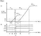
- FIGS. 3(a) and 3(b) disclose a time chart showing an operation of the current circuit breaker.
- FIG. 3(a) shows respective changes with time of current 14 flowing through vacuum circuit breaker 4, current I20 flowing through semiconductor switch 20, stroke ST4 of the driver included in vacuum circuit breaker 4, and stroke ST3 of the driver included in gas disconnector 3.
- FIG. 3(b) shows respective changes with time of control signals ⁇ 3, ⁇ 4, ⁇ 13, and ⁇ 20 for gas disconnector 3, vacuum circuit breaker 4, semiconductor switch 20, and switch 13, respectively.
- FIGS. 3 (a) and 3(b) shows that for normal conduction (initial state), all of the control signals ⁇ 3, ⁇ 4, ⁇ 13, and ⁇ 20 are set to "L" level to cause gas disconnector 3, vacuum circuit breaker 4, and semiconductor switch 20 to be in conducting state, and cause switch 13 to be in non-conducting state. It is supposed that charging of capacitor 11 has been completed and switches 14 and 15 are in non-conducting state.
- a direct current flows through mechanical switch 2 (namely gas disconnector 3 and vacuum circuit breaker 4) while the direct current does not flow through semiconductor switch 20 because a voltage across the terminals of mechanical switch 2 is lower than an ON voltage of semiconductor switch 20. It should be noted, when the voltage across the terminals of mechanical switch 2 exceeds the ON voltage of semiconductor switch 20, the direct current flows through semiconductor switch 20.
- controller 30 When a fault occurs in the DC power transmission system, an open command for causing the DC circuit breaker to be in non-conducting state to interrupt the direct current is given from an external protection relay to controller 30. Initially, at time t1, controller 30 raises control signal ⁇ 4 from "L" level to "H” level to cause the driver of vacuum circuit breaker 4 to start opening operation. Semiconductor switch 20 may normally be in non-conducting state, and semiconductor switch 20 may be caused to be in conducting state at this time (time t1).
- stroke ST4 of the driver in vacuum circuit breaker 4 reaches contacts-open position P1. Then, the contacts of the two electrodes are disconnected from each other and a vacuum arc is generated between the contacts. Since the vacuum arc voltage is on the order of a few volts or less, simple disconnection of the contacts may not be able to cause the vacuum arc voltage to exceed the ON voltage of semiconductor switch 20 and the current may not be commutated from vacuum circuit breaker 4 to semiconductor switch 20 in some cases.
- controller 30 raises control signal ⁇ 13 from "L" level to "H” level to make switch 13 conductive. Accordingly a current in the opposite direction to the direction of the direct current flows from capacitor 11 through reactor 12 and switch 13 to vacuum circuit breaker 4 to generate a zero current point and thereby extinguish the vacuum arc and cause vacuum circuit breaker 4 to be in non-conducting state. Accordingly, the voltage across the terminals of vacuum circuit breaker 4 exceeds the ON voltage of semiconductor switch 20 and the direct current is commutated from vacuum circuit breaker 4 to semiconductor switch 20 (time t4).
- control signal ⁇ 13 is set to "H" level to cause switch 13 of forced commutating circuit 10 to be conductive.
- Capacitor 11 is charged by charger 16 in advance to a voltage value and a polarity that allows flow of a current in the opposite direction to the direction of the fault direct current flowing through vacuum circuit breaker 4. Therefore, when switch 13 is caused to be in conducting state, discharging of capacitor 11 is started and the inverse current is applied to vacuum circuit breaker 4.
- the withstand voltage between the contacts of vacuum circuit breaker 4 may be at least a voltage on the order of a voltage higher than the ON voltage of semiconductor switch 20.
- controller 30 raises at time t5 control signal ⁇ 3 from "L" level to "H” level to cause the driver of gas disconnector 3 to start opening operation.
- stroke ST3 of the driver of gas disconnector 3 reaches contacts-open position P2.
- controller 30 raises control signal ⁇ 20 from "L" level to "H” level to cause semiconductor switch 20 to be in non-conducting state.
- the voltage withstanding capability of vacuum circuit breaker 4 may be lower than the voltage withstanding capability of gas disconnector 3.
- semiconductor switch 20 is configured to have a capability to withstand the voltage applied from the DC power transmission system, interruption of the direct current is completed.
- the direct current is allowed to flow through mechanical switch 2 (namely gas disconnector 3 and vacuum circuit breaker 4) and the power loss can therefore be reduced.
- vacuum circuit breaker 4 having a relatively low voltage withstanding capability may be used and the price of the DC circuit breaker can therefore be reduced.
- the above-described configuration enables a fast and low-cost DC circuit breaker to be obtained.
- a DC circuit breaker which is applicable even to a DC power transmission system of an extra high voltage of 300 kV or more for example and which is capable of interrupting even a fault current of 10 kA or more for example can be obtained.
- a disconnector in which a gas insulating medium such as SF 6 gas is used is employed as gas disconnector 3.
- a vacuum disconnector having its contacts in a vacuum vessel may also be used instead of gas disconnector 3 as long as the vacuum disconnector has a sufficient inter-contact distance that is enough for the vacuum disconnector to withstand a voltage applied to the DC circuit breaker.
- a gas circuit breaker in which an insulating arc-extinguishing medium such as SF 6 gas, nitrogen, argon, air, carbon dioxide, or the like is used may be employed, or a circuit breaker in which a magnetic field of a permanent magnet or electromagnet drives an arc and with this magnetic drive the arc is extinguished may be employed.
- an insulating arc-extinguishing medium such as SF 6 gas, nitrogen, argon, air, carbon dioxide, or the like
- a circuit breaker in which a magnetic field of a permanent magnet or electromagnet drives an arc and with this magnetic drive the arc is extinguished may be employed.
- vacuum circuit breaker 4 is made nonconductive to allow the direct current to be commutated to semiconductor switch 20, gas disconnector 3 is then made nonconductive, and thereafter semiconductor switch 20 is made nonconductive. In this way, the DC circuit breaker is made nonconductive.
- vacuum circuit breaker 4 is caused to start the opening operation (time t1), the two contacts of vacuum circuit breaker 4 are then disconnected from each other (time t2), accordingly gas disconnector 3 is caused to start the opening operation (time t5), the two contacts of gas disconnector 3 are then disconnected from each other (time t6), and accordingly semiconductor switch 20 is made nonconductive (time t7).
- the DC circuit breaker is made nonconductive.
- time T1 time t1 to t2 from the start of the opening operation of vacuum circuit breaker 4 to the disconnection of its two contacts differs from time T2 (time t5 to t6) from the start of the opening operation of gas disconnector 3 to the disconnection of its two contacts.
- FIG. 3 shows that time T1 and T2 meet T1 ⁇ T2.
- control signals ⁇ 4 and ⁇ 3 are raised simultaneously to "H" level as shown in FIGS. 4(a) and 4(b) to cause vacuum circuit breaker 4 and gas disconnector 3 to simultaneously start respective opening operations (time t1).
- time t1 the two contacts of vacuum circuit breaker 4 can be disconnected from each other and thereafter the two contacts of gas disconnector 3 can be disconnected from each other, from which the same effects as those of the first embodiment are obtained.
- the time taken for interrupting a fault current can be shortened by the time by which the opening operation of gas disconnector 3 is made earlier.
- control signals ⁇ 4 and ⁇ 3 are raised simultaneously to "H" level to cause vacuum circuit breaker 4 and gas disconnector 3 to simultaneously start respective opening operations.
- the opening operations may not necessarily be started exactly simultaneously. Within a range of an error due to the performance of controller 30 or the like, there may be some difference in time between the start of one opening operation and the start of the other opening operation.
- vacuum circuit breaker 4 and gas disconnector 3 are caused to start respective opening operations simultaneously.
- gas disconnector 3 may be caused to start its opening operation and thereafter vacuum circuit breaker 4 may be caused to start its opening operation, or vacuum circuit breaker 4 may be caused to start its opening operation and thereafter gas disconnector 3 may be caused to start is opening operation.
- FIG. 5 is a circuit block diagram showing a configuration of a DC circuit breaker in a third embodiment of the present invention, which is to be contrasted with FIG. 1 .
- this DC circuit breaker differs from the DC circuit breaker in FIG. 1 in that vacuum circuit breaker 4 is replaced with a gas circuit breaker 4A, semiconductor switch 20 is replaced with a semiconductor switch 20A, and forced commutating circuit 10 is eliminated.
- gas circuit breaker 4A an insulating arc-extinguishing medium such as SF 6 gas, nitrogen, argon, air, carbon dioxide, or the like fills the space between electrodes.
- Semiconductor switch 20A includes an IGBT 21A formed of SiC. IGBT 21A has a relatively low ON voltage. It is therefore possible to make the arc voltage of gas circuit breaker 4A sufficiently higher than the ON voltage of semiconductor switch 20A (namely the arc resistance of gas circuit breaker 4A can be made sufficiently higher than the ON resistance (the resistance value when the switch is turned on)). Then, without generating a zero current point in gas circuit breaker 4A, the direct current can be commutated to semiconductor switch 20A. Commutation forcing circuit 10 is therefore unnecessary and the price of the DC circuit breaker can be reduced.
- FIG. 6 is a circuit block diagram showing a configuration of a DC circuit breaker in a fourth embodiment of the present invention, which is to be contrasted with FIG. 1 .
- this DC circuit breaker differs from the DC circuit breaker in FIG. 1 in that semiconductor switch 20 is replaced with a semiconductor switch 20B.
- Semiconductor switch 20B additionally includes a capacitor 22 and a resistance element 23 relative to semiconductor switch 20.
- Capacitor 22 and resistance element 23 are connected in series between the collector and the emitter of IGBT 21 to form a snubber circuit for absorbing a surge voltage.
- a plurality of (four in FIG. 7 ) semiconductor switches 20B may be connected in series between upstream electrical path 1a and downstream electrical path 1b.
- FIG. 8 is a circuit block diagram showing a configuration of a DC circuit breaker in a fifth embodiment of the present invention, which is to be contrasted with FIG. 6 .
- this DC circuit breaker differs from the DC circuit breaker in FIG. 6 in that forced commutating circuit 10 is replaced with a forced commutating circuit 10A.
- Commutation forcing circuit 10A additionally includes a resistance element 17 relative to forced commutating circuit 10. Between the gas disconnector 3 side electrode of vacuum circuit breaker 4 and the downstream electrical path 1b side electrode of vacuum circuit breaker 4, resistance element 17, capacitor 11, reactor 12, and switch 13 are connected in series.
- Resistance element 17 may be replaced with reactor 12 or a resistance component of the electrical path in some cases.
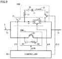
- FIG. 9 is a circuit block diagram showing a configuration of a DC circuit breaker in a sixth embodiment of the present invention, which is to be contrasted with FIG. 8 .
- this DC circuit breaker differs from the DC circuit breaker in FIG. 8 in that forced commutating circuit 10A is replaced with a forced commutating circuit 10B.
- Commutation forcing circuit 10B corresponds to forced commutating circuit 10A from which switches 14 and 15 and charger 16 are removed and to which a battery 18 is added.
- the positive electrode of battery 18 is connected to the electrode, on the downstream electrical path 1b side, of vacuum circuit breaker 4, through capacitor 11, reactor 12, and switch 13, and the negative electrode of battery 18 is connected to the electrode, on the upstream electrical path 1a side, of vacuum circuit breaker 4 through resistance element 17.
- switch 13 When vacuum circuit breaker 4 is caused to be in non-conducting state, switch 13 is caused to be in conducting state and a current in the opposite direction to the direction of the direct current is allowed to flow from battery 18 to vacuum circuit breaker 4 through capacitor 11, reactor 12, and switch 13.
- switches 14 and 15 and charger 16 are unnecessary, and the size of the DC circuit breaker can therefore be reduced.
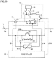
- FIG. 10 is a circuit block diagram showing a configuration of a DC circuit breaker in a seventh embodiment of the present invention, which is to be contrasted with FIG. 6 .
- this DC circuit breaker differs from the DC circuit breaker in FIG. 6 in that the former additionally includes a lighting arrester 25.
- Lighting arrester 25 is connected in parallel with semiconductor switch 20B and absorbs circuit energy after semiconductor switch 20B is made nonconductive to interrupt the direct current.
- the direct current is commutated from semiconductor switch 20B to lighting arrester 25.
- lighting arrester 25 a voltage is generated between terminals depending on the speed of response to a transient change of current during the commutation.
- the direct current is successfully commutated to lighting arrester 25 if each of gas disconnector 3 and semiconductor switch 20B has a voltage withstanding capability to withstand the voltage generated between the terminals of lighting arrester 25.
- the current flowing through lighting arrester 25 is attenuated in accordance with a time constant which is determined by the reactors of lighting arrester 25 and the electrical path. When the current becomes substantially zero, interruption of the direct current is completed.
- the circuit energy can speedily be attenuated after semiconductor switch 20B is made nonconductive.
- FIG. 11 is a circuit block diagram showing a configuration of a DC circuit breaker in an eighth embodiment of the present invention, which is to be contrasted with FIG. 10 .
- this DC circuit breaker differs from the DC circuit breaker in FIG. 10 in that semiconductor switch 20B is replaced with a semiconductor switch 20C.
- Semiconductor switch 20C additionally includes a diode 24 relative to semiconductor switch 20B.
- Diode 24 is connected in antiparallel with IGBT 21. Namely, the anode and the cathode of diode 24 are connected respectively to the emitter and the collector of IGBT 21.
- the current flowing from capacitor 11 to diode 24 is the remaining current.
- the remaining current can be attenuated to be extinguished by resistance element 17 in FIG. 8 for example.
- gas disconnector 3 may be opened. Then, no arc is generated in gas disconnector 3. Similar effects to those of the first embodiment are thus obtained.
- gas disconnector 3 may be designed so that an arc can be extinguished even when a small current like the remaining current flows. In this case, the opening operation can be started without waiting for extinguishing of the arc. Thus, the time to completion of interruption can be shortened, and a fast DC circuit breaker can be obtained. Further, gas disconnector 3 can reliably be interrupted by providing means for assisting arc extinguishing. Specifically, in order to interrupt a small current, a permanent magnet or electromagnet may be used to generate a magnetic force which drives an arc and thereby assists arc extinguishing.
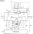
- FIG. 12 is a circuit block diagram showing a configuration of a DC circuit breaker in a ninth embodiment of the present invention, which is to be contrasted with FIG. 11 .
- this DC circuit breaker differs from the DC circuit breaker in FIG. 11 in that the former additionally includes a saturable reactor 26.
- the saturable reactor 26 is connected between the electrode, on the downstream electrical path 1b side, of vacuum circuit breaker 4, and the terminal, on the downstream electrical path 1b side, of switch 13.
- the saturable reactor 26 has its inductance non-linearly changed with respect to the current value, and has a feature that the inductance decreases as the current value increases while the inductance increases as the current value decreases. Since the saturable reactor 26 is provided, the change of the current with time is reduced when the reverse current is supplied from capacitor 11 to vacuum circuit breaker 4 through reactor 12 and switch 13 to thereby cause the current flowing in vacuum circuit breaker 4 to be substantially 0 A. Accordingly, interruption of vacuum circuit breaker 4 is facilitated and commutation of the direct current from vacuum circuit breaker 4 to semiconductor switch 20 is ensured.
Landscapes
- Engineering & Computer Science (AREA)
- Power Engineering (AREA)
- Driving Mechanisms And Operating Circuits Of Arc-Extinguishing High-Tension Switches (AREA)
- Keying Circuit Devices (AREA)
Abstract
Description
- The present invention relates to a DC circuit breaker device, and particularly relates to a DC circuit breaker which opens to interrupt or closes to pass a load current of a DC electric power system in normal state, and interrupts a short-circuit current or a ground-fault current upon occurrence of a fault to thereby protect load equipment.
- An electric power system is equipped with a circuit breaker which interrupts a fault current upon occurrence of a fault. A mechanical AC circuit breaker such as gas circuit breaker, vacuum circuit breaker, and air circuit breaker commonly used in an AC electric power system cannot interrupt the current unless the current value becomes zero. Therefore, the AC circuit breaker interrupts the fault current at a timing when the current value becomes zero which occurs every half cycle of AC.
- Therefore, in order for a mechanical circuit breaker to interrupt a direct current which does not have a zero point due to its nature, it is necessary to take measures to force the current value to become zero.
- There is also a method of interrupting a direct current by means of a semiconductor switch. For this method, the measures to force the current value to become zero are unnecessary, and the current can be interrupted by opening the semiconductor switch. When, however, a load current is conducted through the semiconductor switch in normal conducting state, namely in closed state, Joule heat is generated due to a resistance component of the semiconductor switch and accordingly a power loss is generated. In contrast, a mechanical switch conducts current through its metal contacts, and the power loss is therefore small.
- In a DC circuit breaker for example of Japanese Patent Laid-Open
JP 58-034 525 A - In order to interrupt an extra-high-voltage direct current by semiconductor switches, a DC circuit breaker of
WO2011/057675 includes: a large number of series-connected main semiconductor switches; a smaller number of series-connected auxiliary semiconductor switches relative to the number of the series-connected main semiconductor switches; and a mechanical disconnector connected in series with the auxiliary semiconductor switches and opening at high speed. - Normally, the auxiliary semiconductor switches conduct current. Upon occurrence of a fault, a fault current is commutated from the auxiliary semiconductor switches to the main semiconductor switches and accordingly the fault current is interrupted by the main semiconductor switches.
-
- PTD 1:
- Japanese Patent Laid-Open
JP 58-034 525 A - PTD 2:
-
WO2011/057675 A1 - In order to use the DC circuit breaker of
PTD 1 for an extra-high-voltage power transmission system, it is necessary to connect a large number of GTOs in series and thereby obtain an adequate withstand voltage. In order to commutate a current from the mechanical switch to the series-connected GTOs upon occurrence of a fault, it is necessary to generate, across the mechanical switch, an arc voltage higher than a voltage (ON voltage) at which the series-connected GTOs are turned on. In the case of a vacuum contactor used as the mechanical switch ofPTD 1, however, a sufficient arc voltage may not be generated across the vacuum contactor in some cases. - Moreover, in the DC circuit breaker of
PTD 1, a mechanical disconnector is connected in series with the GTO. The disconnector is opened when a current flowing through a surge absorption device becomes zero. Therefore, a voltage applied across the two terminals of the surge absorption circuit, namely at least a system voltage, is applied to the mechanical switch. The mechanical switch is therefore required to allow an arc voltage to be generated across the mechanical switch and also required to have an inter-electrode voltage withstanding capability in order to withstand an extra high voltage. Accordingly, there arises the need to use an expensive circuit breaker. - In the DC circuit breaker of
PTD 2, a large number of semiconductor switches are connected in series to thereby solve the problem occurring toPTD 1, by use of a disconnector and an auxiliary semiconductor switch, rather than a single mechanical switch. Namely, the DC circuit breaker ofPTD 2 enables commutation to the main semiconductor switches without the need to generate a zero point of the current and enables the disconnector to withstand an extra high voltage. - In this way, the need for the auxiliary semiconductor switch to withstand an extra high voltage applied across the auxiliary semiconductor switch is eliminated. However, while a normal current is flowing through the auxiliary semiconductor switch, a power loss is generated from the auxiliary semiconductor switch.
- A principal object of the present invention is therefore to provide a low-cost DC circuit breaker with a small power loss.
- A DC circuit breaker according to the present invention comprises: a mechanical switch provided on an electrical path through which a direct current flows; and a semiconductor switch connected in parallel with the mechanical switch. The mechanical switch comprises a disconnector and a circuit breaker connected in series. Normally, the direct current flows through the mechanical switch. When interrupting the direct current, the mechanical switch is made nonconductive to allow the direct current to be commutated to the semiconductor switch, and subsequently the semiconductor switch is made nonconductive.
- The DC circuit breaker according to the present invention normally allows a direct current to flow through the mechanical disconnector and circuit breaker, and thus the power loss can be reduced. Moreover, as this circuit breaker, a circuit breaker having a relatively low voltage withstanding capability may be used, and thus the price of the DC circuit breaker can be reduced. Further, the disconnector can be formed with a short gap, and thus the size and the price of the DC circuit breaker can be reduced. In addition, when a direct current is to be interrupted, the direct current is commutated to the semiconductor switch where the current is interrupted. The time taken for interrupting the current can thus be shortened.
-
- FIG. 1
- is a circuit block diagram showing a configuration of a DC circuit breaker in a first embodiment of the present invention.
- FIG. 2
- is a cross-sectional view showing main components of a gas disconnector shown in
FIG. 1 . - FIG. 3
- is a time chart showing an operation of the DC circuit breaker shown in
FIG. 1 . - FIG. 4
- is a time chart showing an operation of a DC circuit breaker in a second embodiment of the present invention.
- FIG. 5
- is a circuit block diagram showing a configuration of a DC circuit breaker in a third embodiment of the present invention.
- FIG. 6
- is a circuit block diagram showing a configuration of a DC circuit breaker in a fourth embodiment of the present invention.
- FIG. 7
- is a circuit block diagram showing a modification of the fourth embodiment.
- FIG. 8
- is a circuit block diagram showing a configuration of a DC circuit breaker in a fifth embodiment of the present invention.
- FIG. 9
- is a circuit block diagram showing a configuration of a DC circuit breaker in a sixth embodiment of the present invention.
- FIG. 10
- is a circuit block diagram showing a configuration of a DC circuit breaker in a seventh embodiment of the present invention.
- FIG. 11
- is a circuit block diagram showing a configuration of a DC circuit breaker in an eighth embodiment of the present invention.
- FIG. 12
- is a circuit block diagram showing a configuration of a DC circuit breaker in a ninth embodiment of the present invention.
-
FIG. 1 is a circuit block diagram showing a configuration of a DC circuit breaker in a first embodiment of the present invention. InFIG. 1 , this DC circuit breaker is provided on anelectrical path 1 of a DC power transmission system, and comprises amechanical switch 2, a forcedcommutating circuit 10, asemiconductor switch 20, and acontroller 30.Mechanical switch 2 comprises agas disconnector 3 and avacuum circuit breaker 4 connected in series between an upstreamelectrical path 1a and a downstreamelectrical path 1b. - The
gas disconnector 3 is controlled by a control signal φ3 from thecontroller 30. Normally, thegas disconnector 3 is caused to be in closed state (conducting state) to pass a direct current. For interruption of the direct current, the direct current is commutated to thesemiconductor switch 20 and thereafter thegas disconnector 3 is caused to be in an opened state (non-conducting state). - The
gas disconnector 3 comprises a tank filled with insulating gas such as SF6, dry air, nitrogen, argon, or carbon dioxide, two electrodes provided in the tank, and a driver causing contacts of the two electrodes to be connected to conduct the current or causing the contacts thereof to be disconnected to interrupt the current. Thegas disconnector 3 has an insulation capability (voltage withstanding capability) which is a capability to withstand a voltage applied to the DC circuit breaker when the distance between the contacts becomes equal to or more than a certain distance. - The driver drives the electrodes using a high speed spring, a hydraulic pressure, an electromagnetic force, or the like. The driver which uses the electromagnetic force may be configured to supplement its driving force with an electromagnetic force generated from a large DC fault current, using an electromagnetic repulsion plate, a driving coil, or the like.
-
FIG. 2 is a cross-sectional view showing main components ofgas disconnector 3. InFIG. 2 , two electrodes EL1 and EL2 are provided so that respective contacts face each other in the tank (not shown) filled with the insulating gas. The contacts of electrodes EL1 and EL2 are caused to be connected to each other or disconnected from each other by the driver (not shown).FIG. 2 shows the state where the contacts of electrodes EL1 and EL2 are disconnected from each other. - In order for a sufficient insulation capability to be exhibited even when the distance between the contacts of electrodes EL1 and EL2 is shortened, electrodes EL1 and EL2 are covered with
respective shields insulator 7 is applied to respective portions ofshields - Referring back to
FIG. 1 , thevacuum circuit breaker 4 is controlled by a control signal φ4 fromcontroller 30. Normally,vacuum circuit breaker 4 is caused to be in closed state (conducting state) to pass a direct current. For interruption of the direct current,vacuum circuit breaker 4 is caused to be in opened state (non-conducting state) to commutate the direct current tosemiconductor switch 20. -
Vacuum circuit breaker 4 comprises a vacuum vessel called vacuum bulb, two electrodes provided in the vacuum vessel, and a driver causing the two electrodes to be connected to conduct the current or causing the two electrodes to be disconnected to interrupt the current. The driver drives the electrodes using a high speed spring, a hydraulic pressure, an electromagnetic force, or the like. - In
vacuum circuit breaker 4, an arc is generated when contacts of the two electrodes are disconnected from each other while the current is conducted. When the distance between the contacts becomes equal to or more than a certain distance, the current can be interrupted by forcing the current to reach the zero value. The insulation capability ofvacuum circuit breaker 4 may be inferior to the insulation capability ofgas disconnector 3. - As the insulation capability between the two electrodes, a capability to withstand a voltage generated between the electrodes while a fault current is allowed to flow through
semiconductor switch 20 in ON state may be enough. As the insulation capability between the electrodes and ground, a capability to withstand a voltage of the DC power transmission system may be enough. - For interruption of a direct current, forced commutating
circuit 10 forces a current to flow tovacuum circuit breaker 4 in the opposite direction to the direction of the direct current flowing throughvacuum circuit breaker 4, to thereby generate a zero current point invacuum circuit breaker 4 and thus causevacuum circuit breaker 4 to be in non-conducting state.Commutation forcing circuit 10 comprises acapacitor 11, areactor 12, switches 13 to 15, and acharger 16.Capacitor 11,reactor 12, and switch 13 are connected in series between an upstream electrode and a downstream electrode ofvacuum circuit breaker 4. -
Capacitor 11 andreactor 12 constitute a resonant circuit.Reactor 12 may be replaced with an inductance component of the electrical path of the circuit in some cases. Asswitch 13, a switch such as vacuum circuit breaker or gas circuit breaker may be used, a gas or vacuum gap switch may be used, or a semiconductor element such as thyristor or IGBT (Insulated Gate Bipolar Transistor) may be used. -
Switch 13 is controlled by control signal φ13 fromcontroller 30. Normally, switch 13 is controlled to be nonconductive. For interruption of a direct current,switch 13 is controlled to be in conducting state. Whenswitch 13 is caused to be in conducting state, a current in the opposite direction to the direction of the direct current is caused to flow fromcapacitor 11 tovacuum circuit breaker 4 through the reactor and switch 13 to thereby force the direct current flowing invacuum circuit breaker 4 to reach zero. In this way,vacuum circuit breaker 4 is caused to be nonconductive. - The negative terminal of
charger 16 is connected throughswitch 14 to the negative electrode ofcapacitor 11, and the positive terminal ofcharger 16 is connected throughswitch 15 to the positive electrode ofcapacitor 11.Switches charger 16 are controlled for example bycontroller 30. For charging, switches 14 and 15 are controlled to be in conducting state, andcharger 16 is controlled to chargecapacitor 11 to a predetermined DC voltage throughswitches - Between upstream
electrical path 1a and downstreamelectrical path 1b,semiconductor switch 20 is connected in parallel withmechanical switch 2.Semiconductor switch 20 is controlled by control signal φ20 fromcontroller 30. For interruption of a direct current,semiconductor switch 20 is caused to be in non-conducting state after allowing flow of the current commutated frommechanical switch 2.Semiconductor switch 20 includes for example a semiconductor element such as IGBT or GTO formed of a semiconductor such as SiC for example, and a driver which causes the semiconductor element to be conductive or nonconductive in response to control signal φ20, and configured in the form of a module.Semiconductor switch 20 may comprise a plurality of parallel or series-connected semiconductor elements.FIG. 1 showssemiconductor switch 20 including oneIGBT 21. -
FIGS. 3(a) and 3(b) disclose a time chart showing an operation of the current circuit breaker.FIG. 3(a) shows respective changes with time of current 14 flowing throughvacuum circuit breaker 4, current I20 flowing throughsemiconductor switch 20, stroke ST4 of the driver included invacuum circuit breaker 4, and stroke ST3 of the driver included ingas disconnector 3.FIG. 3(b) shows respective changes with time of control signals φ3, φ4, φ13, and φ20 forgas disconnector 3,vacuum circuit breaker 4,semiconductor switch 20, and switch 13, respectively. -
FIGS. 3 (a) and 3(b) shows that for normal conduction (initial state), all of the control signals φ3, φ4, φ13, and φ20 are set to "L" level to causegas disconnector 3,vacuum circuit breaker 4, andsemiconductor switch 20 to be in conducting state, and causeswitch 13 to be in non-conducting state. It is supposed that charging ofcapacitor 11 has been completed and switches 14 and 15 are in non-conducting state. - In this condition, a direct current flows through mechanical switch 2 (namely
gas disconnector 3 and vacuum circuit breaker 4) while the direct current does not flow throughsemiconductor switch 20 because a voltage across the terminals ofmechanical switch 2 is lower than an ON voltage ofsemiconductor switch 20. It should be noted, when the voltage across the terminals ofmechanical switch 2 exceeds the ON voltage ofsemiconductor switch 20, the direct current flows throughsemiconductor switch 20. - When a fault occurs in the DC power transmission system, an open command for causing the DC circuit breaker to be in non-conducting state to interrupt the direct current is given from an external protection relay to
controller 30. Initially, at time t1,controller 30 raises control signal φ4 from "L" level to "H" level to cause the driver ofvacuum circuit breaker 4 to start opening operation.Semiconductor switch 20 may normally be in non-conducting state, andsemiconductor switch 20 may be caused to be in conducting state at this time (time t1). - At time t2, stroke ST4 of the driver in
vacuum circuit breaker 4 reaches contacts-open position P1. Then, the contacts of the two electrodes are disconnected from each other and a vacuum arc is generated between the contacts. Since the vacuum arc voltage is on the order of a few volts or less, simple disconnection of the contacts may not be able to cause the vacuum arc voltage to exceed the ON voltage ofsemiconductor switch 20 and the current may not be commutated fromvacuum circuit breaker 4 tosemiconductor switch 20 in some cases. - Next, at time t3,
controller 30 raises control signal φ13 from "L" level to "H" level to makeswitch 13 conductive. Accordingly a current in the opposite direction to the direction of the direct current flows fromcapacitor 11 throughreactor 12 and switch 13 tovacuum circuit breaker 4 to generate a zero current point and thereby extinguish the vacuum arc and causevacuum circuit breaker 4 to be in non-conducting state. Accordingly, the voltage across the terminals ofvacuum circuit breaker 4 exceeds the ON voltage ofsemiconductor switch 20 and the direct current is commutated fromvacuum circuit breaker 4 to semiconductor switch 20 (time t4). - Namely, when the inter-contact distance which is the distance between the contacts of
vacuum circuit breaker 4 reaches a distance that enables current interruption (time t3), control signal φ13 is set to "H" level to causeswitch 13 of forced commutatingcircuit 10 to be conductive.Capacitor 11 is charged bycharger 16 in advance to a voltage value and a polarity that allows flow of a current in the opposite direction to the direction of the fault direct current flowing throughvacuum circuit breaker 4. Therefore, whenswitch 13 is caused to be in conducting state, discharging ofcapacitor 11 is started and the inverse current is applied tovacuum circuit breaker 4. - In
vacuum circuit breaker 4, superimposition of the fault direct current and the inverse current generates a zero current point. At the zero current point,vacuum circuit breaker 4 interrupts the current flowing intovacuum circuit breaker 4. Accordingly, the fault direct current is commutated fromvacuum circuit breaker 4 tosemiconductor switch 20. In order for interruption of the fault direct current to be successful, the withstand voltage between the contacts ofvacuum circuit breaker 4 may be at least a voltage on the order of a voltage higher than the ON voltage ofsemiconductor switch 20. - When the fault direct current is commutated to
semiconductor switch 20 and accordingly no current flows throughgas disconnector 3,controller 30 raises at time t5 control signal φ3 from "L" level to "H" level to cause the driver ofgas disconnector 3 to start opening operation. At time t6, stroke ST3 of the driver ofgas disconnector 3 reaches contacts-open position P2. - When the inter-contact distance of
gas disconnector 3 reaches a distance that is enough forgas disconnector 3 to withstand a voltage which is applied from the system to the DC circuit breaker upon interruption of the fault current by opening of semiconductor switch 20 (time t7),controller 30 raises control signal φ20 from "L" level to "H" level to causesemiconductor switch 20 to be in non-conducting state. - At this time, almost the entire voltage applied to the DC circuit breaker is applied to
gas disconnector 3. Therefore, the voltage withstanding capability ofvacuum circuit breaker 4 may be lower than the voltage withstanding capability ofgas disconnector 3. As long assemiconductor switch 20 is configured to have a capability to withstand the voltage applied from the DC power transmission system, interruption of the direct current is completed. - Thus, in the first embodiment, normally the direct current is allowed to flow through mechanical switch 2 (namely
gas disconnector 3 and vacuum circuit breaker 4) and the power loss can therefore be reduced. Moreover,vacuum circuit breaker 4 having a relatively low voltage withstanding capability may be used and the price of the DC circuit breaker can therefore be reduced. - Moreover, since the opening operation of
gas disconnector 3 is started after current 14 flowing invacuum circuit breaker 4 becomes zero, no arc is generated between the contacts ofgas disconnector 3. The arc is an extremely-high-temperature plasma which reaches 20000 K. Therefore, if a large current arc is maintained for a long time, the contacts are worn to be damaged. In addition, because the gas or air serving as an insulating medium reaches a high temperature, the insulation capability is deteriorated immediately after the arc is extinguished, relative to the case where the contacts are opened without arcing. - However, when the opening operation as described above is performed, no arc is generated in
gas disconnector 3, and therefore, there is no wear or damage of the contacts or no deterioration of the insulation capability. Accordingly, even with a short gap length, a sufficient insulation distance can be obtained. Thus, not only reduction of the size of the DC circuit breaker but also reduction of the time taken for opening the contacts can be achieved and the opening operation can thus be made faster. - Moreover, the above-described configuration enables a fast and low-cost DC circuit breaker to be obtained. Specifically, a DC circuit breaker which is applicable even to a DC power transmission system of an extra high voltage of 300 kV or more for example and which is capable of interrupting even a fault current of 10 kA or more for example can be obtained.
- In the first embodiment, a disconnector in which a gas insulating medium such as SF6 gas is used is employed as
gas disconnector 3. However, a vacuum disconnector having its contacts in a vacuum vessel may also be used instead ofgas disconnector 3 as long as the vacuum disconnector has a sufficient inter-contact distance that is enough for the vacuum disconnector to withstand a voltage applied to the DC circuit breaker. - Moreover, instead of a
vacuum circuit breaker 4, a gas circuit breaker in which an insulating arc-extinguishing medium such as SF6 gas, nitrogen, argon, air, carbon dioxide, or the like is used may be employed, or a circuit breaker in which a magnetic field of a permanent magnet or electromagnet drives an arc and with this magnetic drive the arc is extinguished may be employed. - In the first embodiment,
vacuum circuit breaker 4 is made nonconductive to allow the direct current to be commutated tosemiconductor switch 20,gas disconnector 3 is then made nonconductive, and thereaftersemiconductor switch 20 is made nonconductive. In this way, the DC circuit breaker is made nonconductive. - Namely, as shown in
FIG. 3 ,vacuum circuit breaker 4 is caused to start the opening operation (time t1), the two contacts ofvacuum circuit breaker 4 are then disconnected from each other (time t2), accordinglygas disconnector 3 is caused to start the opening operation (time t5), the two contacts ofgas disconnector 3 are then disconnected from each other (time t6), and accordinglysemiconductor switch 20 is made nonconductive (time t7). In this way, the DC circuit breaker is made nonconductive. - However, time T1 (time t1 to t2) from the start of the opening operation of
vacuum circuit breaker 4 to the disconnection of its two contacts differs from time T2 (time t5 to t6) from the start of the opening operation ofgas disconnector 3 to the disconnection of its two contacts.FIG. 3 shows that time T1 and T2 meet T1 < T2. - Then, in the second embodiment, when the condition T1 < T2 is met, control signals φ4 and φ3 are raised simultaneously to "H" level as shown in
FIGS. 4(a) and 4(b) to causevacuum circuit breaker 4 andgas disconnector 3 to simultaneously start respective opening operations (time t1). Even in this case, the two contacts ofvacuum circuit breaker 4 can be disconnected from each other and thereafter the two contacts ofgas disconnector 3 can be disconnected from each other, from which the same effects as those of the first embodiment are obtained. Moreover, the time taken for interrupting a fault current can be shortened by the time by which the opening operation ofgas disconnector 3 is made earlier. - In the second embodiment, control signals φ4 and φ3 are raised simultaneously to "H" level to cause
vacuum circuit breaker 4 andgas disconnector 3 to simultaneously start respective opening operations. However, the opening operations may not necessarily be started exactly simultaneously. Within a range of an error due to the performance ofcontroller 30 or the like, there may be some difference in time between the start of one opening operation and the start of the other opening operation. - In the second embodiment,
vacuum circuit breaker 4 andgas disconnector 3 are caused to start respective opening operations simultaneously. However, if it is possible to disconnect the two contacts ofvacuum circuit breaker 4 and thereafter disconnect the two contacts ofgas disconnector 3,gas disconnector 3 may be caused to start its opening operation and thereaftervacuum circuit breaker 4 may be caused to start its opening operation, orvacuum circuit breaker 4 may be caused to start its opening operation and thereaftergas disconnector 3 may be caused to start is opening operation. -
FIG. 5 is a circuit block diagram showing a configuration of a DC circuit breaker in a third embodiment of the present invention, which is to be contrasted withFIG. 1 . Referring toFIG. 5 , this DC circuit breaker differs from the DC circuit breaker inFIG. 1 in thatvacuum circuit breaker 4 is replaced with agas circuit breaker 4A,semiconductor switch 20 is replaced with asemiconductor switch 20A, and forcedcommutating circuit 10 is eliminated. Ingas circuit breaker 4A, an insulating arc-extinguishing medium such as SF6 gas, nitrogen, argon, air, carbon dioxide, or the like fills the space between electrodes. - When
gas circuit breaker 4A is caused to perform the opening operation, an arc is generated between its contacts and a higher arc voltage thanvacuum circuit breaker 4 is obtained.Semiconductor switch 20A includes anIGBT 21A formed of SiC.IGBT 21A has a relatively low ON voltage. It is therefore possible to make the arc voltage ofgas circuit breaker 4A sufficiently higher than the ON voltage ofsemiconductor switch 20A (namely the arc resistance ofgas circuit breaker 4A can be made sufficiently higher than the ON resistance (the resistance value when the switch is turned on)). Then, without generating a zero current point ingas circuit breaker 4A, the direct current can be commutated tosemiconductor switch 20A.Commutation forcing circuit 10 is therefore unnecessary and the price of the DC circuit breaker can be reduced. -
FIG. 6 is a circuit block diagram showing a configuration of a DC circuit breaker in a fourth embodiment of the present invention, which is to be contrasted withFIG. 1 . Referring toFIG. 6 , this DC circuit breaker differs from the DC circuit breaker inFIG. 1 in thatsemiconductor switch 20 is replaced with asemiconductor switch 20B. -
Semiconductor switch 20B additionally includes acapacitor 22 and aresistance element 23 relative tosemiconductor switch 20.Capacitor 22 andresistance element 23 are connected in series between the collector and the emitter ofIGBT 21 to form a snubber circuit for absorbing a surge voltage. In this fourth embodiment as well, the same effects as those of the first embodiment are obtained. - As shown in
FIG. 7 , a plurality of (four inFIG. 7 ) semiconductor switches 20B may be connected in series between upstreamelectrical path 1a and downstreamelectrical path 1b. -
FIG. 8 is a circuit block diagram showing a configuration of a DC circuit breaker in a fifth embodiment of the present invention, which is to be contrasted withFIG. 6 . Referring toFIG. 8 , this DC circuit breaker differs from the DC circuit breaker inFIG. 6 in that forced commutatingcircuit 10 is replaced with a forcedcommutating circuit 10A. -
Commutation forcing circuit 10A additionally includes aresistance element 17 relative to forced commutatingcircuit 10. Between thegas disconnector 3 side electrode ofvacuum circuit breaker 4 and the downstreamelectrical path 1b side electrode ofvacuum circuit breaker 4,resistance element 17,capacitor 11,reactor 12, and switch 13 are connected in series. - In the fifth embodiment, when
vacuum circuit breaker 4 is caused to be in non-conducting state, a reverse current applied fromcapacitor 11 tovacuum circuit breaker 4 throughreactor 12 and switch 13 can be attenuated byresistance element 17. -
Resistance element 17 may be replaced withreactor 12 or a resistance component of the electrical path in some cases. -
FIG. 9 is a circuit block diagram showing a configuration of a DC circuit breaker in a sixth embodiment of the present invention, which is to be contrasted withFIG. 8 . Referring toFIG. 9 , this DC circuit breaker differs from the DC circuit breaker inFIG. 8 in that forced commutatingcircuit 10A is replaced with a forcedcommutating circuit 10B. -
Commutation forcing circuit 10B corresponds to forcedcommutating circuit 10A from which switches 14 and 15 andcharger 16 are removed and to which abattery 18 is added. The positive electrode ofbattery 18 is connected to the electrode, on the downstreamelectrical path 1b side, ofvacuum circuit breaker 4, throughcapacitor 11,reactor 12, and switch 13, and the negative electrode ofbattery 18 is connected to the electrode, on the upstreamelectrical path 1a side, ofvacuum circuit breaker 4 throughresistance element 17. Whenvacuum circuit breaker 4 is caused to be in non-conducting state, switch 13 is caused to be in conducting state and a current in the opposite direction to the direction of the direct current is allowed to flow frombattery 18 tovacuum circuit breaker 4 throughcapacitor 11,reactor 12, andswitch 13. - In the sixth embodiment, switches 14 and 15 and
charger 16 are unnecessary, and the size of the DC circuit breaker can therefore be reduced. -
FIG. 10 is a circuit block diagram showing a configuration of a DC circuit breaker in a seventh embodiment of the present invention, which is to be contrasted withFIG. 6 . Referring toFIG. 10 , this DC circuit breaker differs from the DC circuit breaker inFIG. 6 in that the former additionally includes alighting arrester 25.Lighting arrester 25 is connected in parallel withsemiconductor switch 20B and absorbs circuit energy aftersemiconductor switch 20B is made nonconductive to interrupt the direct current. - Namely, when
semiconductor switch 20B is made nonconductive, the direct current is commutated fromsemiconductor switch 20B tolighting arrester 25. Inlighting arrester 25, a voltage is generated between terminals depending on the speed of response to a transient change of current during the commutation. When the voltage between the terminals is higher than the system voltage, the direct current is successfully commutated tolighting arrester 25 if each ofgas disconnector 3 andsemiconductor switch 20B has a voltage withstanding capability to withstand the voltage generated between the terminals oflighting arrester 25. The current flowing throughlighting arrester 25 is attenuated in accordance with a time constant which is determined by the reactors oflighting arrester 25 and the electrical path. When the current becomes substantially zero, interruption of the direct current is completed. - In the seventh embodiment, the circuit energy can speedily be attenuated after
semiconductor switch 20B is made nonconductive. -
FIG. 11 is a circuit block diagram showing a configuration of a DC circuit breaker in an eighth embodiment of the present invention, which is to be contrasted withFIG. 10 . Referring toFIG. 11 , this DC circuit breaker differs from the DC circuit breaker inFIG. 10 in thatsemiconductor switch 20B is replaced with a semiconductor switch 20C. - Semiconductor switch 20C additionally includes a
diode 24 relative tosemiconductor switch 20B.Diode 24 is connected in antiparallel withIGBT 21. Namely, the anode and the cathode ofdiode 24 are connected respectively to the emitter and the collector ofIGBT 21. - When a reverse current is allowed to flow from
capacitor 11 tovacuum circuit breaker 4 throughreactor 12 andswitch 13, the current flows through a path from the positive electrode ofcapacitor 11 to the negative electrode ofcapacitor 11 throughreactor 12,switch 13,diode 24, andgas disconnector 3. Therefore, a remaining voltage ofcapacitor 11 is not applied toIGBT 21. The stress onIGBT 21 is thus reduced. - The current flowing from
capacitor 11 todiode 24 is the remaining current. The remaining current can be attenuated to be extinguished byresistance element 17 inFIG. 8 for example. After the remaining current is extinguished,gas disconnector 3 may be opened. Then, no arc is generated ingas disconnector 3. Similar effects to those of the first embodiment are thus obtained. - Moreover,
gas disconnector 3 may be designed so that an arc can be extinguished even when a small current like the remaining current flows. In this case, the opening operation can be started without waiting for extinguishing of the arc. Thus, the time to completion of interruption can be shortened, and a fast DC circuit breaker can be obtained. Further,gas disconnector 3 can reliably be interrupted by providing means for assisting arc extinguishing. Specifically, in order to interrupt a small current, a permanent magnet or electromagnet may be used to generate a magnetic force which drives an arc and thereby assists arc extinguishing. -
FIG. 12 is a circuit block diagram showing a configuration of a DC circuit breaker in a ninth embodiment of the present invention, which is to be contrasted withFIG. 11 . Referring toFIG. 12 , this DC circuit breaker differs from the DC circuit breaker inFIG. 11 in that the former additionally includes asaturable reactor 26. Thesaturable reactor 26 is connected between the electrode, on the downstreamelectrical path 1b side, ofvacuum circuit breaker 4, and the terminal, on the downstreamelectrical path 1b side, ofswitch 13. - The
saturable reactor 26 has its inductance non-linearly changed with respect to the current value, and has a feature that the inductance decreases as the current value increases while the inductance increases as the current value decreases. Since thesaturable reactor 26 is provided, the change of the current with time is reduced when the reverse current is supplied fromcapacitor 11 tovacuum circuit breaker 4 throughreactor 12 and switch 13 to thereby cause the current flowing invacuum circuit breaker 4 to be substantially 0 A. Accordingly, interruption ofvacuum circuit breaker 4 is facilitated and commutation of the direct current fromvacuum circuit breaker 4 tosemiconductor switch 20 is ensured. - It should be noted that the above-described first to ninth embodiments may of course be combined appropriately.
- It should be construed that the embodiments disclosed herein are given by way of illustration in all respects, not by way of limitation. It is intended that the scope of the present invention is defined by claims, not by the description above, and encompasses all modifications and variations equivalent in meaning and scope to the claims.
-
- 1
- electrical path
- 1a
- upstream electrical path
- 1b
- downstream electrical path
- 3
- gas disconnector
- 4
- vacuum circuit breaker
- 4A
- gas circuit breaker
- EL1, EL2
- electrodes
- 5,6
- shields
- 7
- insulator
- 10, 10A, 10B
- forced commutating circuit
- 11, 22
- capacitor
- 12
- reactor
- 13-15
- switch
- 16
- charger
- 17, 23
- resistance element
- 18
- battery
- 20
- semiconductor switch
- 20A to 20C
- semiconductor switch
- 21
- IGBT
- 21A
- IGBT
- 24
- diode
- 25
- lighting arrester
- 26
- saturable reactor
- 30
- controller
Claims (16)
- A DC circuit breaker comprising:- a mechanical switch provided on an electrical path through which a direct current flows; and- a semiconductor switch connected in parallel with the mechanical switch, the mechanical switch including a disconnector and a circuit breaker connected in series,normally, the direct current flowing through the mechanical switch,
when interrupting the direct current, the mechanical switch being made nonconductive to allow the direct current to be commutated to the semiconductor switch, and subsequently the semiconductor switch being made nonconductive. - The DC circuit breaker according to claim 1,
wherein when interrupting the direct current, the circuit breaker is made nonconductive to allow the direct current to be commutated to the semiconductor switch, and subsequently the disconnector and the semiconductor switch are made nonconductive. - The DC circuit breaker according to claim 2,
wherein contacts of the circuit breaker are disconnected from each other and subsequently contacts of the disconnector are disconnected from each other. - The DC circuit breaker according to claim 3,
wherein opening operation of the circuit breaker is started and subsequently opening operation of the disconnector is started. - The DC circuit breaker according to claim 3,
wherein opening operation of the circuit breaker and opening operation of the disconnector are started simultaneously. - The DC circuit breaker according to claim 1,
wherein an inter-electrode withstand voltage of the circuit breaker is lower than an inter-electrode withstand voltage of the disconnector. - The DC circuit breaker according to claim 1,
further comprising a forced commutating circuit configured to force a current in an opposite direction to a direction of the direct current to flow to the circuit breaker when interrupting the direct current. - The DC circuit breaker according to claim 7,
wherein the forced commutating circuit includes:- a resonance circuit including a capacitor and a reactor connected in series;- a charger configured to charge the capacitor in charging operation; and- a switch configured to connect, in interrupting operation for interrupting the circuit breaker, the resonance circuit to the circuit breaker to allow the current in the opposite direction to the direction of the direct current to flow from the capacitor to the circuit breaker through the reactor. - The DC circuit breaker according to claim 7,
wherein the forced commutating circuit includes:- a battery;- a resonance circuit including a capacitor and a reactor which are connected in series with the battery; and- a switch configured to connect, in interrupting operation for interrupting the circuit breaker, the battery and the resonance circuit to the circuit breaker to allow the current in the opposite direction to the direction of the direct current to flow from the battery to the circuit breaker through the capacitor and the reactor. - The DC circuit breaker according to claim 7,
wherein the forced commutating circuit further includes a resistance element configured to attenuate the current in the opposite direction to the direction of the direct current after the circuit breaker is made nonconductive. - The DC circuit breaker according to claim 7,
further comprising a saturable reactor provided on the electrical path and connected in series with the circuit breaker,
wherein the forced commutating circuit is configured to force the current in the opposite direction to the direction of the direct current to flow to the circuit breaker through the saturable reactor when interrupting the direct current. - The DC circuit breaker according to claim 7,
wherein the circuit breaker is made nonconductive and subsequently the current in the opposite direction to the direction of the direct current is interrupted by the disconnector. - The DC circuit breaker according to claim 1,
wherein the semiconductor switch includes a transistor. - The DC circuit breaker according to claim 13,
wherein the semiconductor switch includes a plurality of the transistors connected in series. - The DC circuit breaker according to claim 13,
wherein the semiconductor switch further includes a diode connected in antiparallel with the transistor. - The DC circuit breaker according to claim 1,
further comprising a lighting arrester connected in parallel with the semiconductor switch and configured to absorb electrical energy after the semiconductor switch is made nonconductive.
Applications Claiming Priority (2)
| Application Number | Priority Date | Filing Date | Title |
|---|---|---|---|
| JP2014196670 | 2014-09-26 | ||
| PCT/JP2015/066291 WO2016047209A1 (en) | 2014-09-26 | 2015-06-05 | Direct current circuit breaker |
Publications (3)
| Publication Number | Publication Date |
|---|---|
| EP3200213A1 true EP3200213A1 (en) | 2017-08-02 |
| EP3200213A4 EP3200213A4 (en) | 2018-06-13 |
| EP3200213B1 EP3200213B1 (en) | 2020-07-22 |
Family
ID=55580750
Family Applications (1)
| Application Number | Title | Priority Date | Filing Date |
|---|---|---|---|
| EP15844233.5A Active EP3200213B1 (en) | 2014-09-26 | 2015-06-05 | Direct current circuit breaker |
Country Status (6)
| Country | Link |
|---|---|
| US (1) | US10910817B2 (en) |
| EP (1) | EP3200213B1 (en) |
| JP (1) | JP6049957B2 (en) |
| CN (1) | CN106716583B (en) |
| DK (1) | DK3200213T3 (en) |
| WO (1) | WO2016047209A1 (en) |
Families Citing this family (15)
| Publication number | Priority date | Publication date | Assignee | Title |
|---|---|---|---|---|
| JP6029772B2 (en) * | 2013-12-11 | 2016-11-24 | 三菱電機株式会社 | DC breaker |
| WO2016042601A1 (en) * | 2014-09-16 | 2016-03-24 | 三菱電機株式会社 | Wind power generation system and dc power feeding system |
| KR101630093B1 (en) * | 2014-12-29 | 2016-06-13 | 주식회사 효성 | High-voltage DC circuit breaker |
| JP6386955B2 (en) * | 2015-03-24 | 2018-09-05 | 株式会社東芝 | DC cutoff device and DC cutoff method |
| JP6448431B2 (en) * | 2015-03-24 | 2019-01-09 | 株式会社東芝 | DC breaker |
| WO2016152147A1 (en) * | 2015-03-24 | 2016-09-29 | 株式会社 東芝 | Direct current interruption device |
| KR102615108B1 (en) * | 2016-12-21 | 2023-12-15 | 한국전기연구원 | Device and method for interrupting dc current by injection of reverse current using vacuum gap switch |
| EP4160641B1 (en) * | 2017-07-11 | 2024-02-28 | Mitsubishi Electric Corporation | Direct-current circuit breaker |
| CN109003851B (en) * | 2017-07-24 | 2020-01-14 | 广州市金矢电子有限公司 | Direct current arc extinguishing circuit and device |
| WO2019117324A1 (en) * | 2017-12-11 | 2019-06-20 | 공주대학교 산학협력단 | Hybrid high-voltage direct current circuit breaker |
| EP3522196B1 (en) * | 2018-01-31 | 2020-11-25 | General Electric Technology GmbH | Switching apparatus |
| JP7183421B2 (en) * | 2019-07-11 | 2022-12-05 | 三菱電機株式会社 | DC distribution board |
| JP7214893B2 (en) * | 2019-11-29 | 2023-01-30 | 株式会社東芝 | DC circuit breaker |
| JP7242575B2 (en) * | 2020-01-06 | 2023-03-20 | 東芝エネルギーシステムズ株式会社 | DC current interrupter |
| CN114788129A (en) * | 2020-11-10 | 2022-07-22 | 东芝三菱电机产业系统株式会社 | Power supply device |
Family Cites Families (25)
| Publication number | Priority date | Publication date | Assignee | Title |
|---|---|---|---|---|
| US3868550A (en) * | 1973-02-16 | 1975-02-25 | Hughes Aircraft Co | Circuit breaker |
| JPS54132776A (en) * | 1978-04-05 | 1979-10-16 | Hitachi Ltd | Dc breaker |
| JPS54149873A (en) | 1978-05-18 | 1979-11-24 | Tokyo Shibaura Electric Co | Breaker |
| JPS55126923A (en) * | 1979-03-22 | 1980-10-01 | Tokyo Shibaura Electric Co | Dc breaker |
| JPS5834525A (en) | 1981-08-21 | 1983-03-01 | 株式会社東芝 | Dc switch |
| JPH0514690Y2 (en) | 1985-06-29 | 1993-04-19 | ||
| US4740858A (en) * | 1985-08-06 | 1988-04-26 | Mitsubishi Denki Kabushiki Kaisha | Zero-current arc-suppression dc circuit breaker |
| JP3135338B2 (en) * | 1992-02-21 | 2001-02-13 | 株式会社日立製作所 | Commutation type DC circuit breaker |
| JPH07161264A (en) | 1993-12-08 | 1995-06-23 | Hitachi Ltd | Large current breaker |
| DE19619437C2 (en) | 1996-05-14 | 2003-01-16 | Abb Schweiz Ag | switchgear |
| JPH10126961A (en) * | 1996-10-17 | 1998-05-15 | Fuji Electric Co Ltd | Current limiting apparatus |
| JP2000048686A (en) * | 1998-07-29 | 2000-02-18 | Hitachi Ltd | Commutation type dc circuit breaker |
| JP2003317582A (en) * | 2002-04-23 | 2003-11-07 | Mitsubishi Electric Corp | Switching device |
| DE202009004198U1 (en) | 2009-03-25 | 2010-08-12 | Ellenberger & Poensgen Gmbh | Isolation switch for galvanic DC interruption |
| NZ599794A (en) | 2009-11-16 | 2013-07-26 | Abb Technology Ag | Direct current circuit breaker with parallel connection of main breaker, auxiliary breaker and non-linear resistor |
| DE102011082568A1 (en) * | 2011-09-13 | 2013-03-14 | Siemens Aktiengesellschaft | DC circuit breaker |
| US8891209B2 (en) * | 2011-11-18 | 2014-11-18 | Abb Technology Ag | HVDC hybrid circuit breaker with snubber circuit |
| ES2911756T3 (en) * | 2011-12-22 | 2022-05-20 | Siemens Energy Global Gmbh & Co Kg | dc hybrid breaker device |
| EP2846342B1 (en) * | 2012-05-01 | 2019-02-06 | Mitsubishi Electric Corporation | Dc circuit breaker |
| DE102012217280A1 (en) * | 2012-09-25 | 2014-03-27 | Siemens Aktiengesellschaft | Separating arrangement for a high voltage direct current network |
| EP3026688B1 (en) * | 2013-07-24 | 2021-01-20 | Mitsubishi Electric Corporation | Semiconductor switch circuit |
| KR101521545B1 (en) * | 2013-10-07 | 2015-05-19 | 한국전기연구원 | Device and method to interrupt high voltage direct current |
| KR20150078491A (en) * | 2013-12-30 | 2015-07-08 | 주식회사 효성 | High-voltage DC circuit breaker |
| KR101550374B1 (en) * | 2013-12-31 | 2015-09-04 | 주식회사 효성 | High-voltage DC circuit breaker |
| CN103762547A (en) * | 2014-01-08 | 2014-04-30 | 西安交通大学 | Modular high-voltage vacuum direct current on-off device based on artificial zero crossing |
-
2015
- 2015-06-05 DK DK15844233.5T patent/DK3200213T3/en active
- 2015-06-05 WO PCT/JP2015/066291 patent/WO2016047209A1/en active Application Filing
- 2015-06-05 US US15/513,858 patent/US10910817B2/en active Active
- 2015-06-05 EP EP15844233.5A patent/EP3200213B1/en active Active
- 2015-06-05 CN CN201580051612.6A patent/CN106716583B/en active Active
- 2015-06-05 JP JP2016549981A patent/JP6049957B2/en active Active
Also Published As
| Publication number | Publication date |
|---|---|
| CN106716583B (en) | 2019-11-22 |
| CN106716583A (en) | 2017-05-24 |
| JP6049957B2 (en) | 2016-12-21 |
| WO2016047209A1 (en) | 2016-03-31 |
| EP3200213A4 (en) | 2018-06-13 |
| US10910817B2 (en) | 2021-02-02 |
| EP3200213B1 (en) | 2020-07-22 |
| US20170288388A1 (en) | 2017-10-05 |
| DK3200213T3 (en) | 2020-08-24 |
| JPWO2016047209A1 (en) | 2017-04-27 |
Similar Documents
| Publication | Publication Date | Title |
|---|---|---|
| EP3200213B1 (en) | Direct current circuit breaker | |
| KR101521545B1 (en) | Device and method to interrupt high voltage direct current | |
| US9948089B2 (en) | DC circuit breaker device | |
| EP3091626B1 (en) | High-voltage dc circuit breaker | |
| JP4913761B2 (en) | Current limiting circuit breaker | |
| US10395866B2 (en) | High voltage DC circuit breaker | |
| US9478974B2 (en) | DC voltage circuit breaker | |
| KR101483084B1 (en) | Device and method to interrupt direct current | |
| CN104137211A (en) | Hvdc hybrid circuit breaker with snubber circuit | |
| Kapoor et al. | State of art of power electronics in circuit breaker technology | |
| KR101766229B1 (en) | Apparatus and method for interrupting high voltage direct current using gap switch | |
| CN108879620B (en) | Direct current breaker based on mechanical switch arc voltage transfer and use method thereof | |
| CN109997208B (en) | Low-voltage circuit breaker device | |
| WO2015166600A1 (en) | Direct current shutoff device | |
| CA3000574A1 (en) | Mechatronic circuit-breaker device | |
| JPWO2019202703A1 (en) | DC circuit breaker | |
| EP3309809B1 (en) | Direct-current interruption apparatus, direct-current interruption method | |
| JP7465997B2 (en) | Solid Isolation Switch | |
| JP2018195565A (en) | Direct current shut-down device | |
| JP2016181382A (en) | Dc cutoff device and dc cutoff method | |
| CN113922330A (en) | Generator outlet circuit breaker based on composite current conversion mode and control method thereof | |
| KR102615108B1 (en) | Device and method for interrupting dc current by injection of reverse current using vacuum gap switch | |
| WO2016199407A1 (en) | Direct-current interruption apparatus, direct-current interruption method | |
| JP2018195547A (en) | Opening/closing device for dc power system | |
| JP2024012743A (en) | Dc component correction part |
Legal Events
| Date | Code | Title | Description |
|---|---|---|---|
| STAA | Information on the status of an ep patent application or granted ep patent |
Free format text: STATUS: THE INTERNATIONAL PUBLICATION HAS BEEN MADE |
|
| PUAI | Public reference made under article 153(3) epc to a published international application that has entered the european phase |
Free format text: ORIGINAL CODE: 0009012 |
|
| STAA | Information on the status of an ep patent application or granted ep patent |
Free format text: STATUS: REQUEST FOR EXAMINATION WAS MADE |
|
| 17P | Request for examination filed |
Effective date: 20170306 |
|
| AK | Designated contracting states |
Kind code of ref document: A1 Designated state(s): AL AT BE BG CH CY CZ DE DK EE ES FI FR GB GR HR HU IE IS IT LI LT LU LV MC MK MT NL NO PL PT RO RS SE SI SK SM TR |
|
| AX | Request for extension of the european patent |
Extension state: BA ME |
|
| DAV | Request for validation of the european patent (deleted) | ||
| DAX | Request for extension of the european patent (deleted) | ||
| A4 | Supplementary search report drawn up and despatched |
Effective date: 20180516 |
|
| RIC1 | Information provided on ipc code assigned before grant |
Ipc: H01H 33/59 20060101AFI20180509BHEP |
|
| GRAP | Despatch of communication of intention to grant a patent |
Free format text: ORIGINAL CODE: EPIDOSNIGR1 |
|
| STAA | Information on the status of an ep patent application or granted ep patent |
Free format text: STATUS: GRANT OF PATENT IS INTENDED |
|
| INTG | Intention to grant announced |
Effective date: 20200206 |
|
| GRAS | Grant fee paid |
Free format text: ORIGINAL CODE: EPIDOSNIGR3 |
|
| GRAA | (expected) grant |
Free format text: ORIGINAL CODE: 0009210 |
|
| STAA | Information on the status of an ep patent application or granted ep patent |
Free format text: STATUS: THE PATENT HAS BEEN GRANTED |
|
| AK | Designated contracting states |
Kind code of ref document: B1 Designated state(s): AL AT BE BG CH CY CZ DE DK EE ES FI FR GB GR HR HU IE IS IT LI LT LU LV MC MK MT NL NO PL PT RO RS SE SI SK SM TR |
|
| REG | Reference to a national code |
Ref country code: GB Ref legal event code: FG4D |
|
| REG | Reference to a national code |
Ref country code: CH Ref legal event code: EP |
|
| REG | Reference to a national code |
Ref country code: DE Ref legal event code: R096 Ref document number: 602015056301 Country of ref document: DE |
|
| REG | Reference to a national code |
Ref country code: AT Ref legal event code: REF Ref document number: 1294194 Country of ref document: AT Kind code of ref document: T Effective date: 20200815 |
|
| REG | Reference to a national code |
Ref country code: IE Ref legal event code: FG4D |
|
| REG | Reference to a national code |
Ref country code: DK Ref legal event code: T3 Effective date: 20200818 |
|
| REG | Reference to a national code |
Ref country code: LT Ref legal event code: MG4D |
|
| REG | Reference to a national code |
Ref country code: AT Ref legal event code: MK05 Ref document number: 1294194 Country of ref document: AT Kind code of ref document: T Effective date: 20200722 |
|
| PG25 | Lapsed in a contracting state [announced via postgrant information from national office to epo] |
Ref country code: FI Free format text: LAPSE BECAUSE OF FAILURE TO SUBMIT A TRANSLATION OF THE DESCRIPTION OR TO PAY THE FEE WITHIN THE PRESCRIBED TIME-LIMIT Effective date: 20200722 Ref country code: ES Free format text: LAPSE BECAUSE OF FAILURE TO SUBMIT A TRANSLATION OF THE DESCRIPTION OR TO PAY THE FEE WITHIN THE PRESCRIBED TIME-LIMIT Effective date: 20200722 Ref country code: HR Free format text: LAPSE BECAUSE OF FAILURE TO SUBMIT A TRANSLATION OF THE DESCRIPTION OR TO PAY THE FEE WITHIN THE PRESCRIBED TIME-LIMIT Effective date: 20200722 Ref country code: SE Free format text: LAPSE BECAUSE OF FAILURE TO SUBMIT A TRANSLATION OF THE DESCRIPTION OR TO PAY THE FEE WITHIN THE PRESCRIBED TIME-LIMIT Effective date: 20200722 Ref country code: LT Free format text: LAPSE BECAUSE OF FAILURE TO SUBMIT A TRANSLATION OF THE DESCRIPTION OR TO PAY THE FEE WITHIN THE PRESCRIBED TIME-LIMIT Effective date: 20200722 Ref country code: BG Free format text: LAPSE BECAUSE OF FAILURE TO SUBMIT A TRANSLATION OF THE DESCRIPTION OR TO PAY THE FEE WITHIN THE PRESCRIBED TIME-LIMIT Effective date: 20201022 Ref country code: PT Free format text: LAPSE BECAUSE OF FAILURE TO SUBMIT A TRANSLATION OF THE DESCRIPTION OR TO PAY THE FEE WITHIN THE PRESCRIBED TIME-LIMIT Effective date: 20201123 Ref country code: GR Free format text: LAPSE BECAUSE OF FAILURE TO SUBMIT A TRANSLATION OF THE DESCRIPTION OR TO PAY THE FEE WITHIN THE PRESCRIBED TIME-LIMIT Effective date: 20201023 Ref country code: NO Free format text: LAPSE BECAUSE OF FAILURE TO SUBMIT A TRANSLATION OF THE DESCRIPTION OR TO PAY THE FEE WITHIN THE PRESCRIBED TIME-LIMIT Effective date: 20201022 Ref country code: AT Free format text: LAPSE BECAUSE OF FAILURE TO SUBMIT A TRANSLATION OF THE DESCRIPTION OR TO PAY THE FEE WITHIN THE PRESCRIBED TIME-LIMIT Effective date: 20200722 |
|
| PG25 | Lapsed in a contracting state [announced via postgrant information from national office to epo] |
Ref country code: LV Free format text: LAPSE BECAUSE OF FAILURE TO SUBMIT A TRANSLATION OF THE DESCRIPTION OR TO PAY THE FEE WITHIN THE PRESCRIBED TIME-LIMIT Effective date: 20200722 Ref country code: RS Free format text: LAPSE BECAUSE OF FAILURE TO SUBMIT A TRANSLATION OF THE DESCRIPTION OR TO PAY THE FEE WITHIN THE PRESCRIBED TIME-LIMIT Effective date: 20200722 Ref country code: PL Free format text: LAPSE BECAUSE OF FAILURE TO SUBMIT A TRANSLATION OF THE DESCRIPTION OR TO PAY THE FEE WITHIN THE PRESCRIBED TIME-LIMIT Effective date: 20200722 Ref country code: IS Free format text: LAPSE BECAUSE OF FAILURE TO SUBMIT A TRANSLATION OF THE DESCRIPTION OR TO PAY THE FEE WITHIN THE PRESCRIBED TIME-LIMIT Effective date: 20201122 |
|
| PG25 | Lapsed in a contracting state [announced via postgrant information from national office to epo] |
Ref country code: NL Free format text: LAPSE BECAUSE OF FAILURE TO SUBMIT A TRANSLATION OF THE DESCRIPTION OR TO PAY THE FEE WITHIN THE PRESCRIBED TIME-LIMIT Effective date: 20200722 |
|
| REG | Reference to a national code |
Ref country code: DE Ref legal event code: R097 Ref document number: 602015056301 Country of ref document: DE |
|
| PG25 | Lapsed in a contracting state [announced via postgrant information from national office to epo] |
Ref country code: RO Free format text: LAPSE BECAUSE OF FAILURE TO SUBMIT A TRANSLATION OF THE DESCRIPTION OR TO PAY THE FEE WITHIN THE PRESCRIBED TIME-LIMIT Effective date: 20200722 Ref country code: SM Free format text: LAPSE BECAUSE OF FAILURE TO SUBMIT A TRANSLATION OF THE DESCRIPTION OR TO PAY THE FEE WITHIN THE PRESCRIBED TIME-LIMIT Effective date: 20200722 Ref country code: EE Free format text: LAPSE BECAUSE OF FAILURE TO SUBMIT A TRANSLATION OF THE DESCRIPTION OR TO PAY THE FEE WITHIN THE PRESCRIBED TIME-LIMIT Effective date: 20200722 Ref country code: IT Free format text: LAPSE BECAUSE OF FAILURE TO SUBMIT A TRANSLATION OF THE DESCRIPTION OR TO PAY THE FEE WITHIN THE PRESCRIBED TIME-LIMIT Effective date: 20200722 Ref country code: CZ Free format text: LAPSE BECAUSE OF FAILURE TO SUBMIT A TRANSLATION OF THE DESCRIPTION OR TO PAY THE FEE WITHIN THE PRESCRIBED TIME-LIMIT Effective date: 20200722 |
|
| PLBE | No opposition filed within time limit |
Free format text: ORIGINAL CODE: 0009261 |
|
| STAA | Information on the status of an ep patent application or granted ep patent |
Free format text: STATUS: NO OPPOSITION FILED WITHIN TIME LIMIT |
|
| PG25 | Lapsed in a contracting state [announced via postgrant information from national office to epo] |
Ref country code: AL Free format text: LAPSE BECAUSE OF FAILURE TO SUBMIT A TRANSLATION OF THE DESCRIPTION OR TO PAY THE FEE WITHIN THE PRESCRIBED TIME-LIMIT Effective date: 20200722 |
|
| 26N | No opposition filed |
Effective date: 20210423 |
|
| PG25 | Lapsed in a contracting state [announced via postgrant information from national office to epo] |
Ref country code: SK Free format text: LAPSE BECAUSE OF FAILURE TO SUBMIT A TRANSLATION OF THE DESCRIPTION OR TO PAY THE FEE WITHIN THE PRESCRIBED TIME-LIMIT Effective date: 20200722 |
|
| PG25 | Lapsed in a contracting state [announced via postgrant information from national office to epo] |
Ref country code: SI Free format text: LAPSE BECAUSE OF FAILURE TO SUBMIT A TRANSLATION OF THE DESCRIPTION OR TO PAY THE FEE WITHIN THE PRESCRIBED TIME-LIMIT Effective date: 20200722 |
|
| REG | Reference to a national code |
Ref country code: NL Ref legal event code: MP Effective date: 20200722 |
|
| PG25 | Lapsed in a contracting state [announced via postgrant information from national office to epo] |
Ref country code: MC Free format text: LAPSE BECAUSE OF FAILURE TO SUBMIT A TRANSLATION OF THE DESCRIPTION OR TO PAY THE FEE WITHIN THE PRESCRIBED TIME-LIMIT Effective date: 20200722 |
|
| REG | Reference to a national code |
Ref country code: CH Ref legal event code: PL |
|
| REG | Reference to a national code |
Ref country code: BE Ref legal event code: MM Effective date: 20210630 |
|
| PG25 | Lapsed in a contracting state [announced via postgrant information from national office to epo] |
Ref country code: LU Free format text: LAPSE BECAUSE OF NON-PAYMENT OF DUE FEES Effective date: 20210605 |
|
| PG25 | Lapsed in a contracting state [announced via postgrant information from national office to epo] |
Ref country code: LI Free format text: LAPSE BECAUSE OF NON-PAYMENT OF DUE FEES Effective date: 20210630 Ref country code: IE Free format text: LAPSE BECAUSE OF NON-PAYMENT OF DUE FEES Effective date: 20210605 Ref country code: CH Free format text: LAPSE BECAUSE OF NON-PAYMENT OF DUE FEES Effective date: 20210630 |
|
| PG25 | Lapsed in a contracting state [announced via postgrant information from national office to epo] |
Ref country code: FR Free format text: LAPSE BECAUSE OF NON-PAYMENT OF DUE FEES Effective date: 20210630 |
|
| PG25 | Lapsed in a contracting state [announced via postgrant information from national office to epo] |
Ref country code: BE Free format text: LAPSE BECAUSE OF NON-PAYMENT OF DUE FEES Effective date: 20210630 |
|
| PG25 | Lapsed in a contracting state [announced via postgrant information from national office to epo] |
Ref country code: HU Free format text: LAPSE BECAUSE OF FAILURE TO SUBMIT A TRANSLATION OF THE DESCRIPTION OR TO PAY THE FEE WITHIN THE PRESCRIBED TIME-LIMIT; INVALID AB INITIO Effective date: 20150605 |
|
| P01 | Opt-out of the competence of the unified patent court (upc) registered |
Effective date: 20230512 |
|
| PG25 | Lapsed in a contracting state [announced via postgrant information from national office to epo] |
Ref country code: CY Free format text: LAPSE BECAUSE OF FAILURE TO SUBMIT A TRANSLATION OF THE DESCRIPTION OR TO PAY THE FEE WITHIN THE PRESCRIBED TIME-LIMIT Effective date: 20200722 |
|
| REG | Reference to a national code |
Ref country code: DE Ref legal event code: R084 Ref document number: 602015056301 Country of ref document: DE |
|
| REG | Reference to a national code |
Ref country code: GB Ref legal event code: 746 Effective date: 20240327 |
|
| PG25 | Lapsed in a contracting state [announced via postgrant information from national office to epo] |
Ref country code: MK Free format text: LAPSE BECAUSE OF FAILURE TO SUBMIT A TRANSLATION OF THE DESCRIPTION OR TO PAY THE FEE WITHIN THE PRESCRIBED TIME-LIMIT Effective date: 20200722 |
|
| PGFP | Annual fee paid to national office [announced via postgrant information from national office to epo] |
Ref country code: GB Payment date: 20240502 Year of fee payment: 10 |
|
| PGFP | Annual fee paid to national office [announced via postgrant information from national office to epo] |
Ref country code: DE Payment date: 20240502 Year of fee payment: 10 |
|
| PGFP | Annual fee paid to national office [announced via postgrant information from national office to epo] |
Ref country code: DK Payment date: 20240612 Year of fee payment: 10 |