EP3199351A1 - Inkjet head and inkjet head manufacturing method - Google Patents
Inkjet head and inkjet head manufacturing method Download PDFInfo
- Publication number
- EP3199351A1 EP3199351A1 EP15843126.2A EP15843126A EP3199351A1 EP 3199351 A1 EP3199351 A1 EP 3199351A1 EP 15843126 A EP15843126 A EP 15843126A EP 3199351 A1 EP3199351 A1 EP 3199351A1
- Authority
- EP
- European Patent Office
- Prior art keywords
- electrode unit
- piezoelectric element
- connecting member
- adjustment member
- lead
- Prior art date
- Legal status (The legal status is an assumption and is not a legal conclusion. Google has not performed a legal analysis and makes no representation as to the accuracy of the status listed.)
- Granted
Links
Images



Classifications
-
- B—PERFORMING OPERATIONS; TRANSPORTING
- B41—PRINTING; LINING MACHINES; TYPEWRITERS; STAMPS
- B41J—TYPEWRITERS; SELECTIVE PRINTING MECHANISMS, i.e. MECHANISMS PRINTING OTHERWISE THAN FROM A FORME; CORRECTION OF TYPOGRAPHICAL ERRORS
- B41J2/00—Typewriters or selective printing mechanisms characterised by the printing or marking process for which they are designed
- B41J2/005—Typewriters or selective printing mechanisms characterised by the printing or marking process for which they are designed characterised by bringing liquid or particles selectively into contact with a printing material
- B41J2/01—Ink jet
- B41J2/135—Nozzles
- B41J2/14—Structure thereof only for on-demand ink jet heads
- B41J2/14201—Structure of print heads with piezoelectric elements
- B41J2/14233—Structure of print heads with piezoelectric elements of film type, deformed by bending and disposed on a diaphragm
-
- B—PERFORMING OPERATIONS; TRANSPORTING
- B41—PRINTING; LINING MACHINES; TYPEWRITERS; STAMPS
- B41J—TYPEWRITERS; SELECTIVE PRINTING MECHANISMS, i.e. MECHANISMS PRINTING OTHERWISE THAN FROM A FORME; CORRECTION OF TYPOGRAPHICAL ERRORS
- B41J2/00—Typewriters or selective printing mechanisms characterised by the printing or marking process for which they are designed
- B41J2/005—Typewriters or selective printing mechanisms characterised by the printing or marking process for which they are designed characterised by bringing liquid or particles selectively into contact with a printing material
- B41J2/01—Ink jet
- B41J2/135—Nozzles
- B41J2/16—Production of nozzles
- B41J2/1607—Production of print heads with piezoelectric elements
- B41J2/161—Production of print heads with piezoelectric elements of film type, deformed by bending and disposed on a diaphragm
-
- B—PERFORMING OPERATIONS; TRANSPORTING
- B41—PRINTING; LINING MACHINES; TYPEWRITERS; STAMPS
- B41J—TYPEWRITERS; SELECTIVE PRINTING MECHANISMS, i.e. MECHANISMS PRINTING OTHERWISE THAN FROM A FORME; CORRECTION OF TYPOGRAPHICAL ERRORS
- B41J2/00—Typewriters or selective printing mechanisms characterised by the printing or marking process for which they are designed
- B41J2/005—Typewriters or selective printing mechanisms characterised by the printing or marking process for which they are designed characterised by bringing liquid or particles selectively into contact with a printing material
- B41J2/01—Ink jet
- B41J2/135—Nozzles
- B41J2/16—Production of nozzles
- B41J2/1621—Manufacturing processes
- B41J2/1623—Manufacturing processes bonding and adhesion
-
- B—PERFORMING OPERATIONS; TRANSPORTING
- B41—PRINTING; LINING MACHINES; TYPEWRITERS; STAMPS
- B41J—TYPEWRITERS; SELECTIVE PRINTING MECHANISMS, i.e. MECHANISMS PRINTING OTHERWISE THAN FROM A FORME; CORRECTION OF TYPOGRAPHICAL ERRORS
- B41J2/00—Typewriters or selective printing mechanisms characterised by the printing or marking process for which they are designed
- B41J2/005—Typewriters or selective printing mechanisms characterised by the printing or marking process for which they are designed characterised by bringing liquid or particles selectively into contact with a printing material
- B41J2/01—Ink jet
- B41J2/135—Nozzles
- B41J2/16—Production of nozzles
- B41J2/1621—Manufacturing processes
- B41J2/1626—Manufacturing processes etching
-
- B—PERFORMING OPERATIONS; TRANSPORTING
- B41—PRINTING; LINING MACHINES; TYPEWRITERS; STAMPS
- B41J—TYPEWRITERS; SELECTIVE PRINTING MECHANISMS, i.e. MECHANISMS PRINTING OTHERWISE THAN FROM A FORME; CORRECTION OF TYPOGRAPHICAL ERRORS
- B41J2/00—Typewriters or selective printing mechanisms characterised by the printing or marking process for which they are designed
- B41J2/005—Typewriters or selective printing mechanisms characterised by the printing or marking process for which they are designed characterised by bringing liquid or particles selectively into contact with a printing material
- B41J2/01—Ink jet
- B41J2/135—Nozzles
- B41J2/16—Production of nozzles
- B41J2/1621—Manufacturing processes
- B41J2/1632—Manufacturing processes machining
-
- B—PERFORMING OPERATIONS; TRANSPORTING
- B41—PRINTING; LINING MACHINES; TYPEWRITERS; STAMPS
- B41J—TYPEWRITERS; SELECTIVE PRINTING MECHANISMS, i.e. MECHANISMS PRINTING OTHERWISE THAN FROM A FORME; CORRECTION OF TYPOGRAPHICAL ERRORS
- B41J2/00—Typewriters or selective printing mechanisms characterised by the printing or marking process for which they are designed
- B41J2/005—Typewriters or selective printing mechanisms characterised by the printing or marking process for which they are designed characterised by bringing liquid or particles selectively into contact with a printing material
- B41J2/01—Ink jet
- B41J2/135—Nozzles
- B41J2/14—Structure thereof only for on-demand ink jet heads
- B41J2002/14362—Assembling elements of heads
-
- B—PERFORMING OPERATIONS; TRANSPORTING
- B41—PRINTING; LINING MACHINES; TYPEWRITERS; STAMPS
- B41J—TYPEWRITERS; SELECTIVE PRINTING MECHANISMS, i.e. MECHANISMS PRINTING OTHERWISE THAN FROM A FORME; CORRECTION OF TYPOGRAPHICAL ERRORS
- B41J2/00—Typewriters or selective printing mechanisms characterised by the printing or marking process for which they are designed
- B41J2/005—Typewriters or selective printing mechanisms characterised by the printing or marking process for which they are designed characterised by bringing liquid or particles selectively into contact with a printing material
- B41J2/01—Ink jet
- B41J2/135—Nozzles
- B41J2/14—Structure thereof only for on-demand ink jet heads
- B41J2002/14491—Electrical connection
-
- B—PERFORMING OPERATIONS; TRANSPORTING
- B41—PRINTING; LINING MACHINES; TYPEWRITERS; STAMPS
- B41J—TYPEWRITERS; SELECTIVE PRINTING MECHANISMS, i.e. MECHANISMS PRINTING OTHERWISE THAN FROM A FORME; CORRECTION OF TYPOGRAPHICAL ERRORS
- B41J2202/00—Embodiments of or processes related to ink-jet or thermal heads
- B41J2202/01—Embodiments of or processes related to ink-jet heads
- B41J2202/18—Electrical connection established using vias
Definitions
- the present invention relates to an inkjet head and a method for manufacturing the inkjet head, particularly relates to the inkjet head capable of reliably achieving electrical connection, with a simple method, in performing electrical connection between an electrode on a head chip and wiring on a wiring substrate by equalizing a height of a contact surface.
- Patent Literature 2 discloses a technique of equalizing the contact state of each of electrical connecting sites and preventing a partial contact failure by allowing the position where the first electrode unit comes in contact with the wiring and the position where the second electrode unit comes in contact with the wiring to have a same height in order to achieve reliable electrical connection between each of the first electrode unit and the second electrode unit formed on the piezoelectric element, with the wiring of the wiring substrate.
- Patent Literatures 1 and 2 has a configuration in which the bump is built on the first electrode unit formed on the piezoelectric element, and thus, an attempt to use high pressure to reliably achieve electrical connection in bonding when the wiring substrate is mutually pasted might cause the pressure to be concentrated on the bump on the surface of the first electrode unit and the damage the piezoelectric element. This leads to a problem of occurrence of demands for high-accuracy pressure control at the time of pressure bonding.
- Patent Literature 2 because of the configuration in which a bump provided on the first electrode unit and a bump provided on the second electrode unit, of the piezoelectric element, are connected with the wiring of the wiring substrate, there may be a case where bonding heights are not even and electrical connection becomes uncertain when the pressure at pressure bonding is not even.
- an object of the present invention is to provide an inkjet head capable of reliably performing electrical connection using a novel and simple configuration that equalizes the height of the contact surface on the electrical connection between the electrode on the head chip and the wiring on the wiring substrate, and a method for manufacturing the inkjet head.
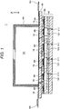
- Fig. 1 is a cross-sectional diagram illustrating an exemplary inkjet head according to the present invention.
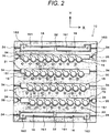
- Fig. 2 is a plan view of a head chip of the inkjet head.
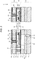
- Fig. 3 is a partially enlarged cross-sectional diagram of the inkjet head.
- An inkjet head 1 has an integrated stacked configuration formed with a head chip 10 and a wiring substrate 20, having a spacer substrate 30 therebetween. On an upper surface of the wiring substrate 20, a box-shaped manifold 40 is arranged. The inside of the manifold 40 is an ink storage chamber 41.
- a Z-direction indicated with an arrow represents “lower” and the opposite direction thereof represents “upper”, relative to a state of the inkjet head 1 in Figs. 1 and 3 .
- the direction with “above” or “up” represents a direction opposite to the Z-direction of the inkjet head 1 and the direction with “below “ or “down” represent a direction along the Z-direction.
- “upper surface” represents a surface arranged in the direction opposite to the Z-direction of the inkjet head 1 and "lower surface” is a direction arranged in the Z-direction.
- the head chip 10 is configured with a nozzle plate 11, an intermediate plate 12, a pressure chamber plate 13, and a vibration plate layer 14, stacked from the lower side in Fig. 3 .
- the pressure chamber plate 13 is formed of a silicon (Si) substrate, for example.
- the pressure chamber plate 13 includes a pressure chamber 131 that contains ink ejected from a nozzle 111 formed on the nozzle plate 11.
- the number of pressure chambers 131 may be any, that is, it is sufficient to have at least one.
- the present embodiment exemplifies the inkjet head 1 including a plurality of the pressure chambers 131.
- the plurality of pressure chambers 131 is arrayed in the X-Y direction of the head chip 10 (refer to Fig. 2 ) when the head chip 10 is seen in plan view.
- the pressure chamber 131 is formed so as to penetrate the pressure chamber plate 13. Accordingly, an upper wall of the pressure chamber 131 is formed with the vibration plate layer 14 and a lower wall is formed with the intermediate plate 12.
- the vibration plate layer 14 is formed of a silicon oxide (SiO2) film, for example.
- the vibration plate layer 14 includes, corresponding to the pressure chamber 131, an ink inflow port 132 that opens onto an upper surface of the head chip 10.
- the intermediate plate 12 is formed of a glass substrate, for example.
- the intermediate plate 12 includes, corresponding to the pressure chamber 131, a plurality of communication passages 121 that communicates with the inside of the pressure chamber 131.
- the nozzle plate 11 is formed of a Si substrate, for example.
- the nozzle plate 11 includes, corresponding to each of the communication passages 121 of the intermediate plate 12, a plurality of nozzles 111 opening onto a lower surface of the nozzle plate 11. Accordingly, the inkjet head 1 according to the present embodiment ejects ink downward from the nozzle 111.
- the piezoelectric element 15 is provided on the upper surface of the head chip 10. Corresponding to each of the pressure chambers 131, the piezoelectric element 15 is arranged on an upper surface of the vibration plate layer 14 that forms an upper wall of the pressure chamber 131.
- the piezoelectric element 15 according to the present embodiment is formed of a PZT thin film having a predetermined thickness. Since it is possible to etch the PZT thin film using a photolithography technology, making it possible to easily form a plurality of piezoelectric elements 15 arrayed in a predetermined pattern.
- the piezoelectric element 15 includes a first electrode unit 151 and a second electrode unit 152.
- the first electrode unit 151 is an individual electrode provided individually for each of the piezoelectric elements 15, formed on an upper surface of the piezoelectric element 15.
- the second electrode unit 152 is a shared electrode for GND provided for the shared use by the plurality of piezoelectric elements 15, formed on a lower surface of the piezoelectric element 15.
- the second electrode unit 152 is formed on the upper surface of the vibration plate layer 14, and the piezoelectric element 15 is mounted on an upper surface of the second electrode unit 152.
- an upper surface of the first electrode unit 151 is arranged at a predetermined height H1 (refer to Fig. 3 ).
- the height H1 at which the upper surface of the first electrode unit 151 is arranged is defined as a height from the upper surface of the vibration plate layer 14 just below the piezoelectric element 15 to the upper surface of the first electrode unit 151, relative to the upper surface of the vibration plate layer 14. There is no bump provided on the upper surface of the first electrode unit 151
- the second electrode unit 152 is formed so as to significantly protrude to the outside of a forming region of the piezoelectric element 15. Specifically, the second electrode unit 152 is formed toward an end portion arranged in a Y-direction of the head chip 10 and toward an end portion arranged in a direction opposite to the Y-direction, illustrated in Fig. 2 , so as to protrude to the outside of the forming region of piezoelectric element 15. With this configuration, a lead-out unit 153 is formed on the upper surface of the vibration plate layer 14. The lead-out unit 153 is formed of an electrode film same as that of the second electrode unit 152 (refer to Fig. 3 ). That is, the second electrode unit 152 is electrically drawn to the outside of the forming region of the piezoelectric element 15 by the lead-out unit 153, on the upper surface of the vibration plate layer 14.
- the second electrode unit 152 is electrically drawn from the lead-out unit 153 shared by the plurality of piezoelectric elements 15. This configuration can integrate the second electrode unit 152 formed on the plurality of piezoelectric elements 15, onto the lead-out unit 153, making it possible to simplify electrical connection toward a plurality of the second electrode units 152.
- An adjustment member 16 is provided on an upper surface of the lead-out unit 153.
- the adjustment member 16 is a member for adjusting the height of an electrical connecting site for achieving electrical continuity between the lead-out unit 153 and a connecting member of the wiring substrate 20 to be described below.
- the adjustment member 16 according to the present embodiment is formed so as to extend along the X-direction illustrated in Fig. 2 , on the upper surface of the lead-out unit 153 drawn in the vicinity of both end portions of the head chip 10.
- the adjustment member 16 may be formed of a single member on the upper surface of the lead-out unit 153, or may be formed by stacking a plurality of layers on the upper surface of the lead-out unit 153.
- Each of the adjustment members 16 in the vicinity of the both end portions of the head chip 10 is divided into two in the X-direction. With this configuration, it is possible to prevent the adjustment member 16 from being deformed or damaged by becoming too elongated. However, it is sufficient to have at least one adjustment member 16 in the present invention.
- the adjustment member 16 is preferably formed of a material having Poisson's ratio of 0.4 or below. Typical Poisson's ratio of the piezoelectric element 15 is approximately 0.3. In addition, Poisson's ratio of gold bump typically used as a first connecting member 25 and a second connecting member 26, to be described below, of the wiring substrate 20 is approximately 0.44. Accordingly, it is possible to allow the first connecting member 25 and the second connecting member 26, connected with the piezoelectric element 15 and the adjustment member 16, to be more easily crushed compared with the piezoelectric element 15 and the adjustment member 16. With this configuration, it is possible to enhance reliability of electrical connection and reduce the load on the piezoelectric element 15.
- a more preferable value is defined as the Poisson' s ratio of the above-described material used as the adjustment member 16, in relation with the piezoelectric element 15. That is, it is more preferable that the adjustment member 16 uses a material having Poisson's ratio substantially equal to the Poisson's ratio of the piezoelectric element 15. This enables the degree of crush in both the connecting members 25 and 26 to be about the same degree when each of the first connecting member 25 and the second connecting member 26 is electrically connected with each of the upper surface of the first electrode unit 151 of the piezoelectric element 15 and an upper surface of the adjustment member 16. Accordingly, it is possible to substantially equalize the pressure applied to the piezoelectric element 15 and the pressure applied to the adjustment member 16, and thus to further enhance reliability of electrical connection and to further reduce the load on the piezoelectric element 15.
- the adjustment member 16 exemplifies a preferred mode using a piezoelectric element of a same material as the piezoelectric element 15 provided for each of the pressure chambers 131, that is, using the PZT thin film. This makes it possible to easily substantially equalize the Poisson' s ratio of the material used as the adjustment member 16 and the piezoelectric element 15. Moreover, it is possible to pattern the both with a same step.
- the adjustment member 16 is formed by providing a third electrode unit 161 on the upper surface of the piezoelectric element.
- the third electrode unit 161 can be formed with a step same as the steps of forming the first electrode unit 151 on the upper surface of the piezoelectric element 15.
- the piezoelectric element 15 and the adjustment member 16 are patterned with a same step, including the first electrode unit 151 and the third electrode unit 161.
- the first electrode unit 151 is provided on the upper surface of the piezoelectric element 15 and the third electrode unit 161 is provided on the upper surface of the adjustment member 16, these electrode units 151 and 161 are formed into sufficiently thin films compared with the piezoelectric element positioned below. Therefore, existence of these electrode units 151 and 161 can be disregarded in the hardness (Poisson's ratio) of the piezoelectric element 15 and the adjustment member 16 in a case where each of the first connecting member 25 and the second connecting member 26 of the wiring substrate 20 is connected with each of the first electrode unit 151 and the third electrode unit 161, respectively.
- the upper surface of the adjustment member 16 is arranged to be substantially equal to the height H1 of the upper surface of the first electrode unit 151. If both surfaces can be patterned with a same step, it would be easy to form the both surfaces such that the height of the upper surfaces of the both can be arranged at a substantially equal height. Accordingly, it is possible to equalize, with a simple method, the height of the upper surface of the first electrode unit 151 and the height of the upper surface of the third electrode unit 161, on the head chip 10 electrically connected with the wiring of the wiring substrate 20.
- the height of the upper surface of the adjustment member 16 is defined as a height from the upper surface of the vibration plate layer 14 just below the piezoelectric element 15 to the upper surface of the third electrode unit 161 of the adjustment member 16, relative to the height of the upper surface of the vibration plate layer 14. There is no bump provided on the upper surface of the third electrode unit 161.
- the height of the upper surface of the adjustment member 16 being “substantially equal” to the height H1 of the upper surface of the first electrode unit 151 means that there may be variation in the height between the two heights, to the degree that can solve the problem of the present invention. Specifically, this mean that the value obtained by subtracting the height of the upper surface of the adjustment member 16 from the value of the height H1 of the upper surface of the first electrode unit 151 is within ⁇ 3% of the value of the height H1 of the upper surface of the first electrode unit 151. Of course, it is preferable that the height of the upper surface of the adjustment member 16 is equal to the height H1 of the upper surface of the first electrode unit 151.
- the height of the upper surface of each of the first electrode unit 151 and the adjustment member 16 corresponds to an individual average value.
- the upper surface of the adjustment member 16 has sufficiently a large area.
- the third electrode unit 161 on the upper surface of the adjustment member 16 has an area equal or greater than the area of the first electrode unit 151 on the upper surface of one piezoelectric element 15. This facilitates positioning in the X-Y direction at the time of performing electrical connection with the connecting member of the wiring substrate 20 to be described below, making it possible to perform bonding operation of the wiring substrate 20 easily.
- a through hole 162 that vertically penetrates the adjustment member 16 is formed on at least a part of the adjustment member 16. This configuration causes the lead-out unit 153 to face the inside of the through hole 162.
- a sufficient amount of conductive material 163 is filled inside the through hole 162.
- the conductive material 163 is a conductive material that is pasty when being filled and that is cured by heating after being filled, and more preferably, the conductive material 163 is conductive adhesive.
- Part of the filled conductive material 163 overflows from the through hole 162, expanding over the third electrode unit 161 around the through hole 162. This allows electrical continuity between the third electrode unit 161 and the lead-out unit 153 via the conductive material 163. There is electrical continuity between the lead-out unit 153 and the second electrode unit 152 on the lower surface of the piezoelectric element 15, leading to electrical continuity between the third electrode unit 161 and second electrode unit 152 via the lead-out unit 153. Note that the conductive material 163 filled within the through hole 162 is cured after bonding of the wiring substrate 20.
- the wiring substrate 20 includes a substrate main body 21 formed of a Si substrate, for example. On the lower surface of the substrate main body 21, there are first wiring 22 and second wiring 23.
- the first wiring 22 is used to achieve electrical connection individually toward the first electrode unit 151 of the plurality of piezoelectric elements 15.
- the second wiring 23 is used to achieve electrical connection that is shared by the second electrode unit 152 of the plurality of piezoelectric elements 15.
- the first wiring 22 is drawn to the upper surface of the substrate main body 21 via a penetrating wiring unit 221 that penetrates the substrate main body 21, and is electrically connected to a first upper wiring unit 222.
- the second wiring 23 is drawn to the upper surface of the substrate main body 21 via a penetrating wiring unit 231 that penetrates the substrate main body 21, and is electrically connected to a second upper wiring unit 232.
- the first upper wiring unit 222 and the second upper wiring unit 232 are electrically connected with an FPC 50 illustrated in Fig. 1 .
- a reference sign 24 represents a protection layer formed of SiO2 and polyimide, for example, provided on upper and lower surfaces of the substrate main body 21 and used for protecting the first wiring 22, the second wiring 23, the first upper wiring unit 222, and the second upper wiring unit 232.
- the first connecting member 25 and the second connecting member 26 are provided on the lower surface of the wiring substrate 20.
- the first connecting member 25 is an electrical connection member connected with the first electrode unit 151 on the head chip 10.
- the second connecting member 26 is an electrical connection member connected with the second electrode unit 152 via the third electrode unit 161 and the lead-out unit 153 on the head chip 10.
- the protection film 24 for the sites on which the first connecting member 25 and the second connecting member 26 are provided is removed, and the first wiring 22 and the second wiring 23 are exposed on the lower surface of the wiring substrate 20.
- the first connecting member 25 has electrical continuity with the first wiring 22 and the second connecting member 26 has electrical continuity with the second wiring 23.
- Each of the first connecting member 25 and the second connecting member 26 is formed in a shape of protrusion, from the lower surface of the wiring substrate 20, in the Z-direction in which the head chip 10 is arranged. Moreover, each of the tip position of the first connecting member 25 and the tip position of the second connecting member 26 is arranged to have a substantially equal height H2 (refer to Fig. 3 ) in the Z-direction in which the head chip 10 is arranged. This configuration facilitates electrical connection with the first electrode unit 151 and the third electrode unit 161, on the head chip 10.
- the height of the tip position of each of the first connecting member 25 and the second connecting member 26 is defined, relative to a contact surface between the first connecting member 25 and the lower surface of the first wiring 22, as a height from the contact surface to the tip position of the first connecting member 25, and a height from the contact surface to the tip position of the second connecting member 26.
- the tip position of the first connecting member 25 and the tip position of the second connecting member 26 being “substantially equal” means that there may be variation in the height between them, to the degree that can solve the problem of the present invention. Specifically, this means that the value obtained by subtracting the height of the tip position of the second connecting member 26 from the height of the tip position of the first connecting member 25 falls within ⁇ 10% of the height of the tip position of the first connecting member 25. Of course, it is preferable that the height of the tip positions of the first connecting member 25 is equal to the height of the second connecting member 26.
- the height of each of the first connecting member 25 and the second connecting member 26 corresponds to an individual average value.
- Each of the first connecting member 25 and the second connecting member 26 is formed of a conductive member.
- the conductive member is preferably a bump, more preferably, a stud bump.
- An exemplary stud bump is formed by first making a metal ball by applying electric discharge and melting to a tip of thin wire of metal such as Au, bonding the metal ball with the surface of each of the first wiring 22 and the second wiring 23 using heat and ultrasound, and tearing the metal thin wire off the metal ball so as to form the bump at a predetermined height of protrusion. This achieve a shape of the stud bump, including, at its base, a plateau-shaped or knob-shaped shoulder portion derived from the metal ball, and a conical shaped side surface.
- the tip portion side of the stud bump includes a protrusion formed of a portion of metal thin wire protruding from the shoulder portion.
- the protrusion is easily plastically deformable and therefore is free from the risk of damaging the piezoelectric element.
- the stud bumping can easily form bumps with various heights of shoulder portion by varying the size of the metal ball, the size of the tip portion and the shoulder portion might differ depending on the size of the stud bump, leading to a difference in the degree of plastic deformation. Accordingly, in view of performing electrical connection more reliably by making plastic deformation on the first connecting member and the second connecting member to be on a similar level at the time of performing electrical connection, it would be preferable that the sizes of the first connecting member and the second connecting member are on a similar level.
- the tip position of the stud bump is a tip position of the protrusion, formed by the metal thin wire torn off from the metal ball.
- each of conductive materials 251 and 261 is applied onto each of the first connecting member 25 and a second connecting portion 26, respectively.
- this configuration even when there is a slight error between the height of the first connecting member 25 and the height of the second connecting portion 26, it is possible to absorb the error, and thus, to further ensure electrical connection between the first connecting member 25 and the first electrode unit 151, and between the second connecting portion 26 and the third electrode unit 161. Moreover, there would be no need to apply excessive pressure at electrical connection.
- each of the conductive materials 251 and 261 is a conductive material that is pasty when being applied and that is cured by heating after being applied, and more preferably, each of the conductive materials 251 and 261 is conductive adhesive.
- conductive adhesive By using conductive adhesive, simultaneous pasting is possible between the first connecting member 25 and the first electrode unit 151, and between the second connecting portion 26 and the third electrode unit 161, in addition to electrical connection between them. This leads to further facilitation of the production steps of the inkjet head 1, including connection of the head chip 10 with the wiring substrate 20.
- a reference sign 27 indicates an ink flow path for supplying the ink within the ink storage chamber 41 (refer to Fig. 1 ) to each of the pressure chambers 131 of the head chip 10 after penetrating the wiring substrate 20.
- the spacer substrate 30 maintains a space between the head chip 10 and the wiring substrate 20 to a predetermined space and ensures a connection region therebetween, for connecting the piezoelectric element 15 with the first connecting member 25, and for connecting the adjustment member 16 with the second connecting member 26.
- the spacer substrate 30 includes openings 31 and 32.
- the opening 31 is formed corresponding to the arrangement position of the piezoelectric element 15 on the head chip 10.
- the opening 32 is formed corresponding to the arrangement position of the adjustment member 16.
- the openings 31 and 32 penetrate the spacer substrate 30, as illustrated in Fig. 3 .
- the piezoelectric element 15 on the head chip 10 and the first connecting member 25 on the wiring substrate 20 are contained within the opening 31.
- the adjustment member 16 on the head chip 10 and the second connecting member 26 on the wiring substrate 20 are contained within the opening 32.
- each of the openings 32 is formed into a size that includes the two adjustment members 16 near each of the end portions of the head chip 10.
- the spacer substrate 30 includes a through hole 33 configured to connect the ink inflow port 132 that opens onto the upper surface of the head chip 10, with the ink flow path 27 formed on the wiring substrate 20.
- the spacer substrate 30 may be formed of any material.
- the spacer substrate 30 uses alloy formed of 42 alloy (42Ni). Suitable surface treatment such as insulation treatment and rustproofing is applied to the spacer substrate 30.
- a reference sign 34 indicates an air release groove for releasing the air within the openings 31 and 32 at the time of bonding of the head chip 10 and the wiring substrate 20, with the spacer member 30 sandwiched therebetween.
- a reference sign 35 indicates a suction groove for sucking the spacer substrate 30 when moving the spacer substrate 30 by a moving apparatus (not illustrated). The air release groove 34 and the suction groove 35 are formed at a depth that would not penetrate the spacer substrate 30, from the upper surface of the spacer substrate 30.
- the head chip 10 and the wiring substrate 20 are bonded with each other, sandwiching the spacer substrate 30 therebetween.
- This bonding enables contact of the first connecting member 25 on the wiring substrate 20 onto the first electrode unit 151 on the piezoelectric element 15 so as to allow electrical connection, and at the same time, and simultaneously enables contact of the second connecting member 26 on the wiring substrate 20 onto the third electrode unit 161 of the adjustment member 16 so as to allow electrical connection.
- the upper surface of the first electrode unit 151 of the piezoelectric element 15 and the upper surface of the third electrode unit 161 of the adjustment member 16 are arranged at the substantially equal height H1, and thus, the heights of the contact surfaces of both are substantially even. Moreover, there is no bump provided on the upper surface of each of the first electrode unit 151 and the third electrode unit 161. Accordingly, at pressure bonding of the head chip 10 with the wiring substrate 20, no uneven pressure is applied to the first electrode unit 151 and the third electrode unit 161. With this configuration, there is no need to perform high-accuracy pressure control to prevent damage on the piezoelectric element 15, or the like, leading to facilitation of reliable electrical connection.
- the tip position of the first connecting member 25 and the tip position of the second connecting member 26 are arranged at a substantially equal height H2, making it possible to further facilitate reliable electrical connection.
- the number of the second connecting member 26 electrically connected with the third electrode unit 161 of one adjustment member 16 is preferably more than one, as illustrated in Fig. 4(a) .
- the plurality of second connecting members 26 it is possible to reduce current density. It is also possible to prevent the pressure at the time of pressure bonding of the second connecting member 26 with the third electrode unit 161 from being concentrated at one point.
- a part of the second connecting members 26 among the plurality of second connecting members 26 is arranged so as to come in contact solely with the conductive material 163 filled into the through hole 162 to achieve electrical connection, as illustrated in Fig. 4(b) .
- a removal portion 241 is formed on the protection layer 24 covering the second wiring 23 so as to expose the second wiring 23 of a site that corresponds to the conductive material 163.
- the conductive material 163 is formed at a height sufficient enough to be able to come in contact with the second wiring 23 exposed within the removal portion 241 when the second connecting portion 26 is electrically connected with the third electrode unit 161.
- the wiring substrate 20 within which the first wiring 22 and the second wiring 23 are formed on the substrate main body 21, is prepared ( Fig. 5(a) ).
- a first connecting portion 25 and the second connecting portion 26 are formed ( Fig. 5(b) ) respectively for each of the first wiring 22 and the second wiring 23 exposed on the lower surface of the wiring substrate 20.
- the first connecting member 25 and the second connecting member 26 are formed (connecting member formation step) such that they have protruding shapes in the direction of arrangement of the head chip 10, and that the tip position of the first connecting portion 25 and the tip position of the second connecting portion 26 are arranged at the substantially equal height H2 in the Z-direction in which the head chip 10 is arranged.
- each of the conductive materials 251 and 261 is applied to each of the first connecting member 25 and the second connecting member 26, as illustrated in Fig. 5(c) .
- the conductive materials 251 and 261 can be applied in the following manner, for example. First, a film, with a predetermined thickness, of the conductive material is formed on a glass substrate. Then, the wiring substrate 20 is stacked on the glass substrate, allowing the tips of the first connecting member 25 and the second connecting member 26 to come in contact with the film of the conductive material. Thereafter, the conductive material on the glass substrate is transferred to the tip of the first connecting member 25 and the second connecting member 26 by separating the wiring substrate 20 from the glass substrate. With this procedure, it is possible to apply conductive material collectively onto tips of a plurality of the first connecting member 25 and a plurality of the second connecting member 26.
- the head chip 10 on which the nozzle plate 11, the intermediate plate 12, the pressure chamber plate 13, and the vibration plate layer 14 are stacked, is prepared ( Fig. 6(a) ).
- the second electrode unit 152 is stacked on the upper surface of the vibration plate layer 14 of the head chip 10.
- the second electrode unit 152 can be formed by a sputtering method, for example, to have a predetermined pattern.
- the lead-out unit 153 electrically drawn from the second electrode unit 152 to the outside of the forming region of the piezoelectric element 15 is simultaneously formed (lead-out unit formation step; Fig. 6(b) ) by extending the pattern of the second electrode unit 152 up to the neighborhood of the both end portions of the head chip 10. This can simplify the lead-out unit formation step.
- the piezoelectric element 15 is stacked on the upper surface of the second electrode unit 152, and adjustment member 16 is stacked on an upper surface of the lead-out unit 153.
- a PZT thin film with a predetermined thickness is stacked on the upper surface of the second electrode unit 152, and then, an electrode film to be the first electrode unit 151 is stacked with a predetermined thickness on a whole upper surface of the PZT thin film.
- the PZT thin film and the electrode film are simultaneously stacked also on the upper surface of the lead-out unit 153.
- the first electrode unit 151 and the third electrode unit 161 are patterned by etching the electrode film so as to achieve arrangement modes and shapes of the piezoelectric element 15 and the adjustment member 16, illustrated in Fig. 2 .
- the piezoelectric element 15 on the pressure chamber 131 and the adjustment member 16 on the lead-out unit 153 are formed (piezoelectric element formation step, adjustment member formation step; Fig. 6(c) ) by etching the PZT thin film using the first electrode unit 151 and the third electrode unit 161 as masks.
- the piezoelectric element 15 and the first electrode unit 151 on the second electrode unit 152, and the adjustment member 16 on the lead-out unit 153 are simultaneously formed with a same step, on the upper surface of the head chip 10.
- This can simplify the manufacturing steps and easily form the piezoelectric element 15 and the adjustment member 16, for which the height of the upper surface of the first electrode unit 151 and the height of the upper surface of the third electrode unit 161 are equalized at the substantially equal height H1.
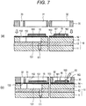
- the spacer substrate 30 is bonded onto the upper surface of the head chip 10 ( Fig. 7(a) ).
- the openings 31 and 32, and the through hole 33, are formed on the spacer substrate 30 beforehand.
- the piezoelectric element 15 and the adjustment member 16 on the head chip 10 are contained within the openings 33 and 32, and the through hole 33 communicates with the ink inflow hole 132.
- a conductive material 162 is filled into the through hole 162 of the adjustment member 16 using a needle 60, for example ( Fig. 7(b) ).
- a needle 60 for example ( Fig. 7(b) ).
- the adjustment member 16 is arranged within the opening 32, the adjustment member 16 is surrounded by a spacer member 30. This configuration can keep the conductive material 162 within the opening 32 even when it overflows from the upper surface of the adjustment member 16 and thus, can prevent a short circuit.
- the wiring substrate 20 is bonded to the stack of the head chip 10 and the spacer substrate 30, from above (bonding step; Fig. 8 ).
- the first connecting member 25 on the wiring substrate 20 comes in contact with the first electrode unit 151 on the piezoelectric element 15, and the second connecting member 26 comes in contact with the third electrode unit 161 of the adjustment member 16, leading to electrical connection respectively.
- the upper surface of the first electrode unit 151 on the piezoelectric element 15 and the upper surface of the third electrode unit 161 of the adjustment member 16 have substantially an equal height on the head chip 10.
- the tip position of the first connecting member 25 and the tip position of the second connecting member 26 have substantially an equal height on the wiring substrate 20. Therefore, these contact surfaces have a substantially even height. Accordingly, when the head chip 10 is pressure bonded with the wiring substrate 20, no uneven pressure is applied to each of electrical connecting sites. With this configuration, there is no need to perform high-accuracy pressure control to prevent damage on the piezoelectric element 15, or the like, leading to further facilitation of reliable electrical connection.
- the manifold 40 illustrated in Fig. 1 is bonded on the upper surface of the wiring substrate 20, such that all ink supply holes 27 that open onto the upper surface of the wiring substrate 20 face the ink storage chamber 41 within the manifold 40.
- This configuration completes the inkjet head 1 in which ink is supplied to all the pressure chambers 131 in a shared manner from the ink storage chamber 41.
- adjustment member 16 forms the through hole 162
- the conductive material 163 is filled into the groove 164 such that the lead-out unit 153 is electrically connected with the third electrode unit 161.
- the piezoelectric element 15 may be a bulk piezoelectric element formed into a predetermined size and thickness in advance.
- the bulk piezoelectric element is individually pasted at a position that corresponds to the pressure chamber 131 on the vibration plate layer 14.
- a bulk piezoelectric element having a thickness equal to the thickness of the piezoelectric element 15 is preferably used as the piezoelectric element used in the adjustment member 16, and the adjustment member 16 is preferably formed by pasting the bulk piezoelectric element on the upper surface of the lead-out unit 153. This makes it possible to easily align the height of the upper surface of the first electrode unit 151 of the piezoelectric element 15 with the height of the upper surface of the adjustment member 16, at a substantially equal height.
- the adjustment member 16 is made from a single material, it is possible to form with metal as a whole.
- a metallic material formed into a predetermined shape with a predetermined thickness using metal such as Ni, Cu, and Al, on the lead-out unit 153 it is possible to provide electrical continuity between the adjustment member 16 itself and the lead-out unit 153.
- metal such as Ni, Cu, and Al
Landscapes
- Engineering & Computer Science (AREA)
- Manufacturing & Machinery (AREA)
- Particle Formation And Scattering Control In Inkjet Printers (AREA)
Abstract
Description
- The present invention relates to an inkjet head and a method for manufacturing the inkjet head, particularly relates to the inkjet head capable of reliably achieving electrical connection, with a simple method, in performing electrical connection between an electrode on a head chip and wiring on a wiring substrate by equalizing a height of a contact surface.
- In recent years, high accuracy and high quality are demanded for images formed by ink ejection from an inkjet head. In a case, for example, where an image is formed by using a line head including a plurality of recording heads arranged across a width direction of a recording medium and by conveying the recording medium to a recording region of the line head, an ejection defect on a nozzle on the line head might cause a stripe and unevenness and degrade the image. Therefore, in order to prevent image degradation and provide a high-accuracy and high-quality image, it is needed to prevent the ejection defect, or the like, in individual nozzles provided on the inkjet head.
- There are various techniques for preventing ejection defects in the nozzle. In a case of an inkjet head that ejects the ink by pressurizing the ink within a pressure chamber communicating with the nozzle by driving piezoelectric elements, it is necessary to reliably supply power to each of the piezoelectric elements in order to reliably drive the piezoelectric elements. Therefore, it is important to achieve reliable electrical connection between each of a first electrode unit (individual electrode) into which driving potential is input and a second electrode unit (shared electrode) into which GND potential is input, formed so as to sandwich the piezoelectric element, with each of wiring of the wiring substrate stacked above the piezoelectric element.
- Specifically, there is a known technique for reliably connecting the first electrode unit of the piezoelectric element with the wiring of the wiring substrate, for example, that uses a partition member formed of resin material to enclose the piezoelectric element so as to maintain a constant space between a head chip with a piezoelectric element and the wiring substrate including wiring, and that performs electrical connection between each of the wiring on the wiring substrate and the electrode formed on each of the piezoelectric elements by allowing a bump provided on a surface of the electrode formed on the piezoelectric element to come in contact with the wiring (Patent Literature 1).
- There is another technique of performing electrical connection by building a bump on a lead-out unit electrically drawn from the second electrode unit formed on the piezoelectric element and allowing the bump to come in contact with the wiring of the wiring substrate, in addition to performing electrical connection by building a bump on the first electrode unit formed on the piezoelectric element and allowing the bump to come in contact with the wiring of the wiring substrate (Patent Literature 2).
- Patent Literature 2 discloses a technique of equalizing the contact state of each of electrical connecting sites and preventing a partial contact failure by allowing the position where the first electrode unit comes in contact with the wiring and the position where the second electrode unit comes in contact with the wiring to have a same height in order to achieve reliable electrical connection between each of the first electrode unit and the second electrode unit formed on the piezoelectric element, with the wiring of the wiring substrate.
-
- Patent Literature 1:
JP 2014-83705 A - Patent Literature 2:
WO 2012/176875 A - Any of
Patent Literatures 1 and 2, however, has a configuration in which the bump is built on the first electrode unit formed on the piezoelectric element, and thus, an attempt to use high pressure to reliably achieve electrical connection in bonding when the wiring substrate is mutually pasted might cause the pressure to be concentrated on the bump on the surface of the first electrode unit and the damage the piezoelectric element. This leads to a problem of occurrence of demands for high-accuracy pressure control at the time of pressure bonding. - Furthermore, in Patent Literature 2, because of the configuration in which a bump provided on the first electrode unit and a bump provided on the second electrode unit, of the piezoelectric element, are connected with the wiring of the wiring substrate, there may be a case where bonding heights are not even and electrical connection becomes uncertain when the pressure at pressure bonding is not even.
- Moreover, even when the pressure is applied evenly, since there are differences in size and height between the bump provided on the first electrode unit and the bump provided on the second electrode unit, this might lead to a different in a deforming amount when pressure bonding is performed. It is, however, difficult to equalize the height of individual contact surfaces by performing pressure control in consideration of the deforming amount.
- Accordingly, an object of the present invention is to provide an inkjet head capable of reliably performing electrical connection using a novel and simple configuration that equalizes the height of the contact surface on the electrical connection between the electrode on the head chip and the wiring on the wiring substrate, and a method for manufacturing the inkjet head.
- Other problems regarding the present invention will be made clear by the following description.
- The above-described problem will be solved by the following invention.
- 1. An inkjet head including:
- a head chip including a pressure chamber configured to contain ink ejected from a nozzle, a piezoelectric element that is provided corresponding to the pressure chamber and includes a first electrode unit on an upper surface and a second electrode unit on a lower surface, and a lead-out unit electrically drawn from the second electrode unit to the outside of the piezoelectric element; and
- a wiring substrate arranged above the head chip and including a first connecting member formed with a stud bump electrically connected with the first electrode unit of the head chip, and a second connecting member formed with a stud bump electrically connected with the second electrode unit via the lead-out unit,
- wherein the lead-out unit includes an adjustment member that includes an upper surface arranged at a height substantially equal to the height of the first electrode unit and in which at least the upper surface has electrical continuity with the lead-out unit, and
- the first connecting member of the wiring substrate is electrically connected with the first electrode unit by coming into contact with an upper surface of the first electrode unit, and the second connecting member is electrically connected with the second electrode unit via the adjustment member and the lead-out unit by coming into contact with the upper surface of the adjustment member.
- 2. The inkjet head according to the above-described 1, wherein the adjustment member is formed of a material having Poisson's ratio of 0.4 or below.
- 3. The inkjet head according to the above-described 1 or 2, wherein the upper surface of the adjustment member has an area that is equal to or larger than the area of the first electrode unit on the upper surface of the piezoelectric element provided corresponding to the pressure chamber.
- 4 . The inkjet head according to the above-described 1, 2, or 3, wherein the adjustment member is formed with the piezoelectric element including, on an upper surface, a third electrode unit having electrical continuity with the lead-out unit.
- 5. The inkjet head according to the above-described 4, wherein the piezoelectric element used in the adjustment member includes a hole penetrating in a height direction or a groove cut across the height direction, and
the third electrode unit and the lead-out unit are electrically connected with each other via a conductive material by filling the conductive material into the hole or the groove. - 6. The inkjet head according to the above-described 5, wherein there is a plurality of the second connecting members, and a part of the second connecting members among the plurality of second connecting members is in contact solely with the conductive material filled into the hole or the groove.
- 7. The inkjet head according to any one of the above-described 1 to 5, wherein there is a plurality of the second connecting members, and the plurality of second connecting members is electrically connected with the upper surface of the adjustment member shared by the plurality of second connecting members.
- 8. The inkjet head according to any one of the above-described 1 to 7, wherein there is a plurality of the pressure chambers, and the individual second electrode units formed on a plurality of the piezoelectric elements provided corresponding to the pressure chambers are electrically drawn by the lead-out unit that is shared by the plurality of second electrode units.
- 9. The inkjet head according to any one of the above-described 1 to 8, wherein tip positions of the first connecting member and the second connecting member are arranged at substantially equal heights in a direction of arrangement of the head chip.
- 10. The inkjet head according to any one of the above-described 1 to 9, wherein each of the first connecting member and the second connecting member has a conductive material applied, and is electrically connected with the upper surface of the first electrode unit and the upper surface of the adjustment member, via the conductive material.
- 11. A method for manufacturing an inkjet head including:
- a head chip including a pressure chamber configured to contain ink ejected from a nozzle, a piezoelectric element that is provided corresponding to the pressure chamber and includes a first electrode unit on an upper surface and a second electrode unit on a lower surface, and a lead-out unit electrically drawn from the second electrode unit to the outside of the piezoelectric element; and
- a wiring substrate arranged above the head chip and including a first connecting member electrically connected with the first electrode unit of the head chip, and a second connecting member electrically connected with the second electrode unit via the lead-out unit,
- the method including:
- a piezoelectric element formation step of forming, on the head chip, the piezoelectric element including the first electrode unit and the second electrode unit, corresponding to the pressure chamber;
- a lead-out unit formation step of forming the lead-out unit on the head chip;
- an adjustment member formation step of forming, on the lead-out unit, an adjustment member that includes an upper surface arranged at a height substantially equal to the height of the first electrode unit, the upper surface having electrical continuity with the lead-out unit; and
- a bonding step of bonding the wiring substrate with the head chip so as to cause the first connecting member to be electrically connected with the first electrode unit by bringing the first connecting member into contact with an upper surface of the first electrode unit, and to cause the second connecting member to be electrically connected with the second electrode unit via the adjustment member by bringing the second connecting member into contact with the upper surface of the adjustment member.
- 12. The method for manufacturing an inkjet head according to the above-described 11,
wherein the adjustment member is formed with the piezoelectric element including, on an upper surface, a third electrode unit that has electrical continuity with the lead-out unit, and
the piezoelectric element used in the adjustment member is formed, in the adjustment member formation step, simultaneously at the time of forming the piezoelectric element corresponding to the pressure chamber by the piezoelectric element formation step. - 13. The method for manufacturing an inkjet head according to the above-described 12,
wherein the piezoelectric element is a PZT thin film, and the piezoelectric element corresponding to the pressure chamber and the piezoelectric element used in the adjustment member are patterned simultaneously by etching the PZT thin film. - 14. The method for manufacturing an inkjet head according to the above-described 11, 12, or 13, further including:
- a connecting member formation step of forming, on the wiring substrate, the first connecting member and the second connecting member so as to have protruding shapes in a direction of arrangement of the head chip, and so as to allow tip positions of the connecting members to be arranged at substantially equal heights in the direction of arrangement of the head chip.
-
-
Fig. 1 is a cross-sectional diagram illustrating an exemplary inkjet head according to the present invention. -
Fig. 2 is a plan view of a head chip of the inkjet head. -
Fig. 3 is a partially enlarged cross-sectional diagram of the inkjet head. -
Figs. 4(a) to 4(c) are cross-sectional diagrams illustrating other modes of connection configurations between a second connecting member of a wiring substrate and an adjustment member. -
Figs. 5(a) to 5(c) are diagrams illustrating manufacturing steps of the inkjet head according to the present invention. -
Figs. 6(a) to 6(c) are diagrams illustrating manufacturing steps of the inkjet head according to the present invention. -
Figs. 7(a) and 7(b) are diagrams illustrating a method for manufacturing the inkjet head according to the present invention. -
Fig. 8 is a diagram illustrating a method for manufacturing the inkjet head according to the present invention. -
Fig. 9 is a partial plan view illustrating other mode of the adjustment member. - Hereinafter, an embodiment of the present invention will be described in detail with reference to the drawings.
-
Fig. 1 is a cross-sectional diagram illustrating an exemplary inkjet head according to the present invention.Fig. 2 is a plan view of a head chip of the inkjet head.Fig. 3 is a partially enlarged cross-sectional diagram of the inkjet head. - An
inkjet head 1 has an integrated stacked configuration formed with ahead chip 10 and awiring substrate 20, having aspacer substrate 30 therebetween. On an upper surface of thewiring substrate 20, a box-shapedmanifold 40 is arranged. The inside of the manifold 40 is anink storage chamber 41. - Note that, in a case where "upper" or "lower" is indicated in the present invention, a Z-direction indicated with an arrow represents "lower" and the opposite direction thereof represents "upper", relative to a state of the
inkjet head 1 inFigs. 1 and3 . Accordingly, the direction with "above" or "up" represents a direction opposite to the Z-direction of theinkjet head 1 and the direction with "below " or "down" represent a direction along the Z-direction. Moreover, "upper surface" represents a surface arranged in the direction opposite to the Z-direction of theinkjet head 1 and "lower surface" is a direction arranged in the Z-direction. - The
head chip 10 is configured with anozzle plate 11, anintermediate plate 12, apressure chamber plate 13, and avibration plate layer 14, stacked from the lower side inFig. 3 . - The
pressure chamber plate 13 is formed of a silicon (Si) substrate, for example. Thepressure chamber plate 13 includes apressure chamber 131 that contains ink ejected from anozzle 111 formed on thenozzle plate 11. The number ofpressure chambers 131 may be any, that is, it is sufficient to have at least one. The present embodiment exemplifies theinkjet head 1 including a plurality of thepressure chambers 131. - The plurality of
pressure chambers 131 is arrayed in the X-Y direction of the head chip 10 (refer toFig. 2 ) when thehead chip 10 is seen in plan view. Thepressure chamber 131 is formed so as to penetrate thepressure chamber plate 13. Accordingly, an upper wall of thepressure chamber 131 is formed with thevibration plate layer 14 and a lower wall is formed with theintermediate plate 12. - The
vibration plate layer 14 is formed of a silicon oxide (SiO2) film, for example. Thevibration plate layer 14 includes, corresponding to thepressure chamber 131, anink inflow port 132 that opens onto an upper surface of thehead chip 10. - The
intermediate plate 12 is formed of a glass substrate, for example. Theintermediate plate 12 includes, corresponding to thepressure chamber 131, a plurality ofcommunication passages 121 that communicates with the inside of thepressure chamber 131. - The
nozzle plate 11 is formed of a Si substrate, for example. Thenozzle plate 11 includes, corresponding to each of thecommunication passages 121 of theintermediate plate 12, a plurality ofnozzles 111 opening onto a lower surface of thenozzle plate 11. Accordingly, theinkjet head 1 according to the present embodiment ejects ink downward from thenozzle 111. - The
piezoelectric element 15 is provided on the upper surface of thehead chip 10. Corresponding to each of thepressure chambers 131, thepiezoelectric element 15 is arranged on an upper surface of thevibration plate layer 14 that forms an upper wall of thepressure chamber 131. Thepiezoelectric element 15 according to the present embodiment is formed of a PZT thin film having a predetermined thickness. Since it is possible to etch the PZT thin film using a photolithography technology, making it possible to easily form a plurality ofpiezoelectric elements 15 arrayed in a predetermined pattern. - The
piezoelectric element 15 includes afirst electrode unit 151 and asecond electrode unit 152. Thefirst electrode unit 151 is an individual electrode provided individually for each of thepiezoelectric elements 15, formed on an upper surface of thepiezoelectric element 15. Thesecond electrode unit 152 is a shared electrode for GND provided for the shared use by the plurality ofpiezoelectric elements 15, formed on a lower surface of thepiezoelectric element 15. Thesecond electrode unit 152 is formed on the upper surface of thevibration plate layer 14, and thepiezoelectric element 15 is mounted on an upper surface of thesecond electrode unit 152. - With this configuration, an upper surface of the
first electrode unit 151 is arranged at a predetermined height H1 (refer toFig. 3 ). Note that, in the present invention, the height H1 at which the upper surface of thefirst electrode unit 151 is arranged is defined as a height from the upper surface of thevibration plate layer 14 just below thepiezoelectric element 15 to the upper surface of thefirst electrode unit 151, relative to the upper surface of thevibration plate layer 14. There is no bump provided on the upper surface of thefirst electrode unit 151 - The
second electrode unit 152 is formed so as to significantly protrude to the outside of a forming region of thepiezoelectric element 15. Specifically, thesecond electrode unit 152 is formed toward an end portion arranged in a Y-direction of thehead chip 10 and toward an end portion arranged in a direction opposite to the Y-direction, illustrated inFig. 2 , so as to protrude to the outside of the forming region ofpiezoelectric element 15. With this configuration, a lead-outunit 153 is formed on the upper surface of thevibration plate layer 14. The lead-outunit 153 is formed of an electrode film same as that of the second electrode unit 152 (refer toFig. 3 ). That is, thesecond electrode unit 152 is electrically drawn to the outside of the forming region of thepiezoelectric element 15 by the lead-outunit 153, on the upper surface of thevibration plate layer 14. - Moreover, the
second electrode unit 152 is electrically drawn from the lead-outunit 153 shared by the plurality ofpiezoelectric elements 15. This configuration can integrate thesecond electrode unit 152 formed on the plurality ofpiezoelectric elements 15, onto the lead-outunit 153, making it possible to simplify electrical connection toward a plurality of thesecond electrode units 152. - An
adjustment member 16 is provided on an upper surface of the lead-outunit 153. Theadjustment member 16 is a member for adjusting the height of an electrical connecting site for achieving electrical continuity between the lead-outunit 153 and a connecting member of thewiring substrate 20 to be described below. For example, theadjustment member 16 according to the present embodiment is formed so as to extend along the X-direction illustrated inFig. 2 , on the upper surface of the lead-outunit 153 drawn in the vicinity of both end portions of thehead chip 10. - The
adjustment member 16 may be formed of a single member on the upper surface of the lead-outunit 153, or may be formed by stacking a plurality of layers on the upper surface of the lead-outunit 153. - Each of the
adjustment members 16 in the vicinity of the both end portions of thehead chip 10 is divided into two in the X-direction. With this configuration, it is possible to prevent theadjustment member 16 from being deformed or damaged by becoming too elongated. However, it is sufficient to have at least oneadjustment member 16 in the present invention. - The
adjustment member 16 is preferably formed of a material having Poisson's ratio of 0.4 or below. Typical Poisson's ratio of thepiezoelectric element 15 is approximately 0.3. In addition, Poisson's ratio of gold bump typically used as a first connectingmember 25 and a second connectingmember 26, to be described below, of thewiring substrate 20 is approximately 0.44. Accordingly, it is possible to allow the first connectingmember 25 and the second connectingmember 26, connected with thepiezoelectric element 15 and theadjustment member 16, to be more easily crushed compared with thepiezoelectric element 15 and theadjustment member 16. With this configuration, it is possible to enhance reliability of electrical connection and reduce the load on thepiezoelectric element 15. - A more preferable value is defined as the Poisson' s ratio of the above-described material used as the
adjustment member 16, in relation with thepiezoelectric element 15. That is, it is more preferable that theadjustment member 16 uses a material having Poisson's ratio substantially equal to the Poisson's ratio of thepiezoelectric element 15. This enables the degree of crush in both the connectingmembers member 25 and the second connectingmember 26 is electrically connected with each of the upper surface of thefirst electrode unit 151 of thepiezoelectric element 15 and an upper surface of theadjustment member 16. Accordingly, it is possible to substantially equalize the pressure applied to thepiezoelectric element 15 and the pressure applied to theadjustment member 16, and thus to further enhance reliability of electrical connection and to further reduce the load on thepiezoelectric element 15. - The
adjustment member 16 according to the present embodiment exemplifies a preferred mode using a piezoelectric element of a same material as thepiezoelectric element 15 provided for each of thepressure chambers 131, that is, using the PZT thin film. This makes it possible to easily substantially equalize the Poisson' s ratio of the material used as theadjustment member 16 and thepiezoelectric element 15. Moreover, it is possible to pattern the both with a same step. - The
adjustment member 16 according to the present embodiment is formed by providing athird electrode unit 161 on the upper surface of the piezoelectric element. Thethird electrode unit 161 can be formed with a step same as the steps of forming thefirst electrode unit 151 on the upper surface of thepiezoelectric element 15. Specifically, thepiezoelectric element 15 and theadjustment member 16 are patterned with a same step, including thefirst electrode unit 151 and thethird electrode unit 161. - Note that, while the
first electrode unit 151 is provided on the upper surface of thepiezoelectric element 15 and thethird electrode unit 161 is provided on the upper surface of theadjustment member 16, theseelectrode units electrode units piezoelectric element 15 and theadjustment member 16 in a case where each of the first connectingmember 25 and the second connectingmember 26 of thewiring substrate 20 is connected with each of thefirst electrode unit 151 and thethird electrode unit 161, respectively. - The upper surface of the
adjustment member 16 is arranged to be substantially equal to the height H1 of the upper surface of thefirst electrode unit 151. If both surfaces can be patterned with a same step, it would be easy to form the both surfaces such that the height of the upper surfaces of the both can be arranged at a substantially equal height. Accordingly, it is possible to equalize, with a simple method, the height of the upper surface of thefirst electrode unit 151 and the height of the upper surface of thethird electrode unit 161, on thehead chip 10 electrically connected with the wiring of thewiring substrate 20. - Note that, in the present invention, the height of the upper surface of the
adjustment member 16 is defined as a height from the upper surface of thevibration plate layer 14 just below thepiezoelectric element 15 to the upper surface of thethird electrode unit 161 of theadjustment member 16, relative to the height of the upper surface of thevibration plate layer 14. There is no bump provided on the upper surface of thethird electrode unit 161. - Note that, the height of the upper surface of the
adjustment member 16 being "substantially equal" to the height H1 of the upper surface of thefirst electrode unit 151 means that there may be variation in the height between the two heights, to the degree that can solve the problem of the present invention. Specifically, this mean that the value obtained by subtracting the height of the upper surface of theadjustment member 16 from the value of the height H1 of the upper surface of thefirst electrode unit 151 is within ±3% of the value of the height H1 of the upper surface of thefirst electrode unit 151. Of course, it is preferable that the height of the upper surface of theadjustment member 16 is equal to the height H1 of the upper surface of thefirst electrode unit 151. - Note that, in a case where the number of each of the
piezoelectric element 15 and theadjustment member 16 is more than one, the height of the upper surface of each of thefirst electrode unit 151 and theadjustment member 16 corresponds to an individual average value. - As illustrated in
Fig. 2 , the upper surface of theadjustment member 16 has sufficiently a large area. Specifically, thethird electrode unit 161 on the upper surface of theadjustment member 16 has an area equal or greater than the area of thefirst electrode unit 151 on the upper surface of onepiezoelectric element 15. This facilitates positioning in the X-Y direction at the time of performing electrical connection with the connecting member of thewiring substrate 20 to be described below, making it possible to perform bonding operation of thewiring substrate 20 easily. - A through
hole 162 that vertically penetrates theadjustment member 16 is formed on at least a part of theadjustment member 16. This configuration causes the lead-outunit 153 to face the inside of the throughhole 162. In addition, a sufficient amount ofconductive material 163 is filled inside the throughhole 162. Preferably, theconductive material 163 is a conductive material that is pasty when being filled and that is cured by heating after being filled, and more preferably, theconductive material 163 is conductive adhesive. - Part of the filled
conductive material 163 overflows from the throughhole 162, expanding over thethird electrode unit 161 around the throughhole 162. This allows electrical continuity between thethird electrode unit 161 and the lead-outunit 153 via theconductive material 163. There is electrical continuity between the lead-outunit 153 and thesecond electrode unit 152 on the lower surface of thepiezoelectric element 15, leading to electrical continuity between thethird electrode unit 161 andsecond electrode unit 152 via the lead-outunit 153. Note that theconductive material 163 filled within the throughhole 162 is cured after bonding of thewiring substrate 20. - The
wiring substrate 20 includes a substratemain body 21 formed of a Si substrate, for example. On the lower surface of the substratemain body 21, there arefirst wiring 22 andsecond wiring 23. Thefirst wiring 22 is used to achieve electrical connection individually toward thefirst electrode unit 151 of the plurality ofpiezoelectric elements 15. Thesecond wiring 23 is used to achieve electrical connection that is shared by thesecond electrode unit 152 of the plurality ofpiezoelectric elements 15. - The
first wiring 22 is drawn to the upper surface of the substratemain body 21 via a penetratingwiring unit 221 that penetrates the substratemain body 21, and is electrically connected to a firstupper wiring unit 222. Moreover, thesecond wiring 23 is drawn to the upper surface of the substratemain body 21 via a penetratingwiring unit 231 that penetrates the substratemain body 21, and is electrically connected to a secondupper wiring unit 232. On an end portion of thewiring substrate 20, the firstupper wiring unit 222 and the secondupper wiring unit 232 are electrically connected with anFPC 50 illustrated inFig. 1 . - In
Fig. 3 , areference sign 24 represents a protection layer formed of SiO2 and polyimide, for example, provided on upper and lower surfaces of the substratemain body 21 and used for protecting thefirst wiring 22, thesecond wiring 23, the firstupper wiring unit 222, and the secondupper wiring unit 232. - The first connecting
member 25 and the second connectingmember 26 are provided on the lower surface of thewiring substrate 20. The first connectingmember 25 is an electrical connection member connected with thefirst electrode unit 151 on thehead chip 10. The second connectingmember 26 is an electrical connection member connected with thesecond electrode unit 152 via thethird electrode unit 161 and the lead-outunit 153 on thehead chip 10. Theprotection film 24 for the sites on which the first connectingmember 25 and the second connectingmember 26 are provided is removed, and thefirst wiring 22 and thesecond wiring 23 are exposed on the lower surface of thewiring substrate 20. The first connectingmember 25 has electrical continuity with thefirst wiring 22 and the second connectingmember 26 has electrical continuity with thesecond wiring 23. - Each of the first connecting
member 25 and the second connectingmember 26 is formed in a shape of protrusion, from the lower surface of thewiring substrate 20, in the Z-direction in which thehead chip 10 is arranged. Moreover, each of the tip position of the first connectingmember 25 and the tip position of the second connectingmember 26 is arranged to have a substantially equal height H2 (refer toFig. 3 ) in the Z-direction in which thehead chip 10 is arranged. This configuration facilitates electrical connection with thefirst electrode unit 151 and thethird electrode unit 161, on thehead chip 10. - Note that the height of the tip position of each of the first connecting
member 25 and the second connectingmember 26 is defined, relative to a contact surface between the first connectingmember 25 and the lower surface of thefirst wiring 22, as a height from the contact surface to the tip position of the first connectingmember 25, and a height from the contact surface to the tip position of the second connectingmember 26. - Note that the tip position of the first connecting
member 25 and the tip position of the second connectingmember 26 being "substantially equal" means that there may be variation in the height between them, to the degree that can solve the problem of the present invention. Specifically, this means that the value obtained by subtracting the height of the tip position of the second connectingmember 26 from the height of the tip position of the first connectingmember 25 falls within ±10% of the height of the tip position of the first connectingmember 25. Of course, it is preferable that the height of the tip positions of the first connectingmember 25 is equal to the height of the second connectingmember 26. - Note that, in a case where there is a plurality of the first connecting
member 25 and a plurality of the second connectingmembers 26, the height of each of the first connectingmember 25 and the second connectingmember 26 corresponds to an individual average value. - Each of the first connecting
member 25 and the second connectingmember 26 is formed of a conductive member. The conductive member is preferably a bump, more preferably, a stud bump. An exemplary stud bump is formed by first making a metal ball by applying electric discharge and melting to a tip of thin wire of metal such as Au, bonding the metal ball with the surface of each of thefirst wiring 22 and thesecond wiring 23 using heat and ultrasound, and tearing the metal thin wire off the metal ball so as to form the bump at a predetermined height of protrusion. This achieve a shape of the stud bump, including, at its base, a plateau-shaped or knob-shaped shoulder portion derived from the metal ball, and a conical shaped side surface. Additionally, the tip portion side of the stud bump includes a protrusion formed of a portion of metal thin wire protruding from the shoulder portion. The protrusion is easily plastically deformable and therefore is free from the risk of damaging the piezoelectric element. While the stud bumping can easily form bumps with various heights of shoulder portion by varying the size of the metal ball, the size of the tip portion and the shoulder portion might differ depending on the size of the stud bump, leading to a difference in the degree of plastic deformation. Accordingly, in view of performing electrical connection more reliably by making plastic deformation on the first connecting member and the second connecting member to be on a similar level at the time of performing electrical connection, it would be preferable that the sizes of the first connecting member and the second connecting member are on a similar level. Note that the tip position of the stud bump is a tip position of the protrusion, formed by the metal thin wire torn off from the metal ball. - It would be preferable, as illustrated in
Fig. 3 , each ofconductive materials member 25 and a second connectingportion 26, respectively. With this configuration, even when there is a slight error between the height of the first connectingmember 25 and the height of the second connectingportion 26, it is possible to absorb the error, and thus, to further ensure electrical connection between the first connectingmember 25 and thefirst electrode unit 151, and between the second connectingportion 26 and thethird electrode unit 161. Moreover, there would be no need to apply excessive pressure at electrical connection. - Preferably, each of the
conductive materials conductive materials member 25 and thefirst electrode unit 151, and between the second connectingportion 26 and thethird electrode unit 161, in addition to electrical connection between them. This leads to further facilitation of the production steps of theinkjet head 1, including connection of thehead chip 10 with thewiring substrate 20. - Note that in
Fig. 3 , areference sign 27 indicates an ink flow path for supplying the ink within the ink storage chamber 41 (refer toFig. 1 ) to each of thepressure chambers 131 of thehead chip 10 after penetrating thewiring substrate 20. - The
spacer substrate 30 maintains a space between thehead chip 10 and thewiring substrate 20 to a predetermined space and ensures a connection region therebetween, for connecting thepiezoelectric element 15 with the first connectingmember 25, and for connecting theadjustment member 16 with the second connectingmember 26. In order to ensure this connection region, thespacer substrate 30 includesopenings opening 31 is formed corresponding to the arrangement position of thepiezoelectric element 15 on thehead chip 10. Theopening 32 is formed corresponding to the arrangement position of theadjustment member 16. - The
openings spacer substrate 30, as illustrated inFig. 3 . Thepiezoelectric element 15 on thehead chip 10 and the first connectingmember 25 on thewiring substrate 20 are contained within theopening 31. Theadjustment member 16 on thehead chip 10 and the second connectingmember 26 on thewiring substrate 20 are contained within theopening 32. - In the
head chip 10 according to the present embodiment, as illustrated inFig. 2 , eightpiezoelectric elements 15 are arrayed in the X-direction, and four rows of the eightpiezoelectric elements 15 are arrayed in the Y-direction. Oneopening 31 is formed in a size that includes the eightpiezoelectric elements 15 arrayed in the X-direction. Accordingly, the fouropenings 31 are arrayed in the Y-direction. Moreover, each of theopenings 32 is formed into a size that includes the twoadjustment members 16 near each of the end portions of thehead chip 10. - Additionally, the
spacer substrate 30 includes a throughhole 33 configured to connect theink inflow port 132 that opens onto the upper surface of thehead chip 10, with theink flow path 27 formed on thewiring substrate 20. - The
spacer substrate 30 may be formed of any material. Herein, thespacer substrate 30 uses alloy formed of 42 alloy (42Ni). Suitable surface treatment such as insulation treatment and rustproofing is applied to thespacer substrate 30. - In
Fig. 2 , areference sign 34 indicates an air release groove for releasing the air within theopenings head chip 10 and thewiring substrate 20, with thespacer member 30 sandwiched therebetween. Moreover, areference sign 35 indicates a suction groove for sucking thespacer substrate 30 when moving thespacer substrate 30 by a moving apparatus (not illustrated). Theair release groove 34 and thesuction groove 35 are formed at a depth that would not penetrate thespacer substrate 30, from the upper surface of thespacer substrate 30. - The
head chip 10 and thewiring substrate 20 are bonded with each other, sandwiching thespacer substrate 30 therebetween. This bonding enables contact of the first connectingmember 25 on thewiring substrate 20 onto thefirst electrode unit 151 on thepiezoelectric element 15 so as to allow electrical connection, and at the same time, and simultaneously enables contact of the second connectingmember 26 on thewiring substrate 20 onto thethird electrode unit 161 of theadjustment member 16 so as to allow electrical connection. - At this time, the upper surface of the
first electrode unit 151 of thepiezoelectric element 15 and the upper surface of thethird electrode unit 161 of theadjustment member 16 are arranged at the substantially equal height H1, and thus, the heights of the contact surfaces of both are substantially even. Moreover, there is no bump provided on the upper surface of each of thefirst electrode unit 151 and thethird electrode unit 161. Accordingly, at pressure bonding of thehead chip 10 with thewiring substrate 20, no uneven pressure is applied to thefirst electrode unit 151 and thethird electrode unit 161. With this configuration, there is no need to perform high-accuracy pressure control to prevent damage on thepiezoelectric element 15, or the like, leading to facilitation of reliable electrical connection. - Moreover, the tip position of the first connecting
member 25 and the tip position of the second connectingmember 26 are arranged at a substantially equal height H2, making it possible to further facilitate reliable electrical connection. - The number of the second connecting
member 26 electrically connected with thethird electrode unit 161 of oneadjustment member 16 is preferably more than one, as illustrated inFig. 4(a) . By using the plurality of second connectingmembers 26, it is possible to reduce current density. It is also possible to prevent the pressure at the time of pressure bonding of the second connectingmember 26 with thethird electrode unit 161 from being concentrated at one point. - It would be also preferable that a part of the second connecting
members 26 among the plurality of second connectingmembers 26 is arranged so as to come in contact solely with theconductive material 163 filled into the throughhole 162 to achieve electrical connection, as illustrated inFig. 4(b) . By allowing a part of the second connectingmember 26 to come in contact with theconductive material 163 prior to curing, it is possible to achieve electrical connection between the second connectingportion 26 and thethird electrode unit 161 and simultaneously achieve ensured fixing between the second connectingportion 26 and thethird electrode unit 161. - Furthermore, in addition to allowing the second connecting
member 26 to come in contact with the upper surface of thethird electrode unit 161, it would be also allowable to achieve electrical connection of thesecond wiring 23 of thewiring substrate 20 with theconductive material 163 of theadjustment member 16 by direct contact, as illustrated inFig. 4(c) . In this case, aremoval portion 241 is formed on theprotection layer 24 covering thesecond wiring 23 so as to expose thesecond wiring 23 of a site that corresponds to theconductive material 163. Moreover, theconductive material 163 is formed at a height sufficient enough to be able to come in contact with thesecond wiring 23 exposed within theremoval portion 241 when the second connectingportion 26 is electrically connected with thethird electrode unit 161. - Next, an exemplary method for manufacturing an inkjet head will be described with reference to
Figs. 5 to 8 . - First, the
wiring substrate 20 will be described. - Using a known method, the
wiring substrate 20 within which thefirst wiring 22 and thesecond wiring 23 are formed on the substratemain body 21, is prepared (Fig. 5(a) ). - Subsequently, using the stud bump, a first connecting
portion 25 and the second connectingportion 26 are formed (Fig. 5(b) ) respectively for each of thefirst wiring 22 and thesecond wiring 23 exposed on the lower surface of thewiring substrate 20. Specifically, the first connectingmember 25 and the second connectingmember 26 are formed (connecting member formation step) such that they have protruding shapes in the direction of arrangement of thehead chip 10, and that the tip position of the first connectingportion 25 and the tip position of the second connectingportion 26 are arranged at the substantially equal height H2 in the Z-direction in which thehead chip 10 is arranged. - After formation of the stud bump, each of the
conductive materials member 25 and the second connectingmember 26, as illustrated inFig. 5(c) . - The
conductive materials wiring substrate 20 is stacked on the glass substrate, allowing the tips of the first connectingmember 25 and the second connectingmember 26 to come in contact with the film of the conductive material. Thereafter, the conductive material on the glass substrate is transferred to the tip of the first connectingmember 25 and the second connectingmember 26 by separating thewiring substrate 20 from the glass substrate. With this procedure, it is possible to apply conductive material collectively onto tips of a plurality of the first connectingmember 25 and a plurality of the second connectingmember 26. - Next, the
head chip 10 will be described. - First, using a known method, the
head chip 10 on which thenozzle plate 11, theintermediate plate 12, thepressure chamber plate 13, and thevibration plate layer 14 are stacked, is prepared (Fig. 6(a) ). - Subsequently, the
second electrode unit 152 is stacked on the upper surface of thevibration plate layer 14 of thehead chip 10. Thesecond electrode unit 152 can be formed by a sputtering method, for example, to have a predetermined pattern. At this time, the lead-outunit 153 electrically drawn from thesecond electrode unit 152 to the outside of the forming region of thepiezoelectric element 15 is simultaneously formed (lead-out unit formation step;Fig. 6(b) ) by extending the pattern of thesecond electrode unit 152 up to the neighborhood of the both end portions of thehead chip 10. This can simplify the lead-out unit formation step. - Next, the
piezoelectric element 15 is stacked on the upper surface of thesecond electrode unit 152, andadjustment member 16 is stacked on an upper surface of the lead-outunit 153. Specifically, a PZT thin film with a predetermined thickness is stacked on the upper surface of thesecond electrode unit 152, and then, an electrode film to be thefirst electrode unit 151 is stacked with a predetermined thickness on a whole upper surface of the PZT thin film. The PZT thin film and the electrode film are simultaneously stacked also on the upper surface of the lead-outunit 153. - Thereafter, the
first electrode unit 151 and thethird electrode unit 161 are patterned by etching the electrode film so as to achieve arrangement modes and shapes of thepiezoelectric element 15 and theadjustment member 16, illustrated inFig. 2 . Subsequently, thepiezoelectric element 15 on thepressure chamber 131 and theadjustment member 16 on the lead-outunit 153 are formed (piezoelectric element formation step, adjustment member formation step;Fig. 6(c) ) by etching the PZT thin film using thefirst electrode unit 151 and thethird electrode unit 161 as masks. - With this procedure, corresponding to the
pressure chamber 131, thepiezoelectric element 15 and thefirst electrode unit 151 on thesecond electrode unit 152, and theadjustment member 16 on the lead-outunit 153 are simultaneously formed with a same step, on the upper surface of thehead chip 10. This can simplify the manufacturing steps and easily form thepiezoelectric element 15 and theadjustment member 16, for which the height of the upper surface of thefirst electrode unit 151 and the height of the upper surface of thethird electrode unit 161 are equalized at the substantially equal height H1. - Next, the
spacer substrate 30 is bonded onto the upper surface of the head chip 10 (Fig. 7(a) ). Theopenings hole 33, are formed on thespacer substrate 30 beforehand. Thepiezoelectric element 15 and theadjustment member 16 on thehead chip 10 are contained within theopenings hole 33 communicates with theink inflow hole 132. - Thereafter, a
conductive material 162 is filled into the throughhole 162 of theadjustment member 16 using aneedle 60, for example (Fig. 7(b) ). By filling a sufficient amount of theconductive material 162, it is possible to allow it to overflow from the upper end of the throughhole 162 and to expand over thethird electrode unit 161 around the throughhole 162. - This allows electrical continuity between the
third electrode unit 161 and the lead-outunit 153 easily via theconductive material 163. Moreover, since theadjustment member 16 is arranged within theopening 32, theadjustment member 16 is surrounded by aspacer member 30. This
configuration can keep theconductive material 162 within theopening 32 even when it overflows from the upper surface of theadjustment member 16 and thus, can prevent a short circuit. - Next, the
wiring substrate 20 is bonded to the stack of thehead chip 10 and thespacer substrate 30, from above (bonding step;Fig. 8 ). At this time, the first connectingmember 25 on thewiring substrate 20 comes in contact with thefirst electrode unit 151 on thepiezoelectric element 15, and the second connectingmember 26 comes in contact with thethird electrode unit 161 of theadjustment member 16, leading to electrical connection respectively. - The upper surface of the
first electrode unit 151 on thepiezoelectric element 15 and the upper surface of thethird electrode unit 161 of theadjustment member 16 have
substantially an equal height on thehead chip 10. Moreover, the tip position of the first connectingmember 25 and the tip position of the second connectingmember 26 have substantially an equal height on thewiring substrate 20. Therefore, these contact surfaces have a substantially even height.
Accordingly, when thehead chip 10 is pressure bonded with thewiring substrate 20, no uneven pressure is applied to each of electrical connecting sites. With this configuration, there is no need to perform high-accuracy pressure control to prevent damage on thepiezoelectric element 15, or the like, leading to further facilitation of reliable electrical connection. - Thereafter, the manifold 40 illustrated in
Fig. 1 is bonded on the upper surface of thewiring substrate 20, such that all ink supply holes 27 that open onto the upper surface of thewiring substrate 20 face theink storage chamber 41 within themanifold 40. This configuration completes theinkjet head 1 in which ink is supplied to all thepressure chambers 131 in a shared manner from theink storage chamber 41. - While the above-described
adjustment member 16 forms the throughhole 162, it would also allowable to form, in place of the throughhole 162, agroove 164 cut across a height direction of theadjustment member 16 such that it forms a recess inwardly from a side surface of theadjustment member 16, as illustrated inFig. 9 . In this case, theconductive material 163 is filled into thegroove 164 such that the lead-outunit 153 is electrically connected with thethird electrode unit 161. - Moreover, the
piezoelectric element 15 may be a bulk piezoelectric element formed into a predetermined size and thickness in advance. The bulk piezoelectric element is individually pasted at a position that corresponds to thepressure chamber 131 on thevibration plate layer 14. In this case, a bulk piezoelectric element having a thickness equal to the thickness of thepiezoelectric element 15 is preferably used as the piezoelectric element used in theadjustment member 16, and theadjustment member 16 is preferably formed by pasting the bulk piezoelectric element on the upper surface of the lead-outunit 153. This makes it possible to easily align the height of the upper surface of thefirst electrode unit 151 of thepiezoelectric element 15 with the height of the upper surface of theadjustment member 16, at a substantially equal height. - Moreover, in a case where the
adjustment member 16 is made from a single material, it is possible to form with metal as a whole. By stacking a metallic material formed into a predetermined shape with a predetermined thickness using metal such as Ni, Cu, and Al, on the lead-outunit 153, it is possible to provide electrical continuity between theadjustment member 16 itself and the lead-outunit 153. By providing a metallic material on the upper surface of the lead-outunit 153 and thereafter grinding it so as to be a height substantially equal to the height of the upper surface of thepiezoelectric element 15, it is possible to adjust the height of the upper surface of theadjustment member 16 to be a height substantially equal to the height of the upper surface of thefirst electrode unit 151 of thepiezoelectric element 15. By forming the whole of theadjustment member 16 with metal, operation of filling theconductive material 163 can be omitted. -
- 1
- inkjet head
- 10
- head chip
- 11
- nozzle plate
- 111
- nozzle
- 12
- intermediate plate
- 121
- communication passage
- 13
- pressure chamber plate
- 131
- pressure chamber
- 132
- ink inflow hole
- 14
- vibration plate layer
- 15
- piezoelectric element
- 151
- first electrode unit
- 152
- second electrode unit
- 153
- lead-out unit
- 16
- adjustment member
- 161
- third electrode unit
- 162
- through hole
- 163
- conductive material
- 164
- groove
- 20
- wiring substrate
- 21
- substrate main body
- 22
- first wiring
- 221
- penetrating wiring unit
- 222
- first upper wiring unit
- 23
- second wiring
- 231
- penetrating wiring unit
- 232
- second upper wiring unit
- 24
- protection layer
- 241
- removal portion
- 25
- first connecting member
- 251
- conductive material
- 26
- second connecting member
- 261
- conductive material
- 27
- ink supply hole
- 30
- spacer substrate
- 31, 32
- opening
- 33
- through hole
- 34
- air release groove
- 35
- suction groove
- 40
- manifold
- 41
- ink storage chamber
- 50
- FPC
- 60
- needle
Claims (14)
- An inkjet head comprising:a head chip including a pressure chamber configured to contain ink ejected from a nozzle, a piezoelectric element that is provided corresponding to the pressure chamber and includes a first electrode unit on an upper surface and a second electrode unit on a lower surface, and a lead-out unit electrically drawn from the second electrode unit to the outside of the piezoelectric element; anda wiring substrate arranged above the head chip and including a first connecting member formed with a stud bump electrically connected with the first electrode unit of the head chip, and a second connecting member formed with a stud bump electrically connected with the second electrode unit via the lead-out unit,wherein the lead-out unit includes an adjustment member that includes an upper surface arranged at a height substantially equal to the height of the first electrode unit and in which at least the upper surface has electrical continuity with the lead-out unit, andthe first connecting member of the wiring substrate is electrically connected with the first electrode unit by coming into contact with an upper surface of the first electrode unit, and the second connecting member is electrically connected with the second electrode unit via the adjustment member and the lead-out unit by coming into contact with the upper surface of the adjustment member.
- The inkjet head according to claim 1,
wherein the adjustment member is formed of a material having Poisson's ratio of 0.4 or below. - The inkjet head according to claim 1 or 2,
wherein the upper surface of the adjustment member has an area that is equal to or larger than the area of the first electrode unit on the upper surface of the piezoelectric element provided corresponding to the pressure chamber. - The inkjet head according to claim 1, 2, or 3,
wherein the adjustment member is formed with the piezoelectric element including, on an upper surface, a third electrode unit having electrical continuity with the lead-out unit. - The inkjet head according to claim 4,
wherein the piezoelectric element used in the adjustment member includes a hole penetrating in a height direction or a groove cut across the height direction, and
the third electrode unit and the lead-out unit are electrically connected with each other via a conductive material by filling the conductive material into the hole or the groove. - The inkjet head according to claim 5,
wherein there is a plurality of the second connecting members, and a part of the second connecting members among the plurality of second connecting members is in contact solely with the conductive material filled into the hole or the groove. - The inkjet head according to any one of claims 1 to 5,
wherein there is a plurality of the second connecting members, and the plurality of second connecting members is electrically connected with the upper surface of the adjustment member shared by the plurality of second connecting members. - The inkjet head according to any one of claims 1 to 7,
wherein there is a plurality of the pressure chambers, and the individual second electrode units formed on a plurality of the piezoelectric elements provided corresponding to the pressure chambers are electrically drawn by the lead-out unit that is shared by the plurality of second electrode units. - The inkjet head according to any one of claims 1 to 8,
wherein tip positions of the first connecting member and the second connecting member are arranged at substantially equal heights in a direction of arrangement of the head chip. - The inkjet head according to any one of claims 1 to 9,
wherein each of the first connecting member and the second connecting member has a conductive material applied, and is electrically connected with the upper surface of the first electrode unit and the upper surface of the adjustment member, via the conductive material. - A method for manufacturing an inkjet head comprising:a head chip including a pressure chamber configured to contain ink ejected from a nozzle, a piezoelectric element that is provided corresponding to the pressure chamber and includes a first electrode unit on an upper surface and a second electrode unit on a lower surface, and a lead-out unit electrically drawn from the second electrode unit to the outside of the piezoelectric element; anda wiring substrate arranged above the head chip and including a first connecting member electrically connected with the first electrode unit of the head chip, and a second connecting member electrically connected with the second electrode unit via the lead-out unit,the method comprising:a piezoelectric element formation step of forming, on the head chip, the piezoelectric element including the first electrode unit and the second electrode unit, corresponding to the pressure chamber;a lead-out unit formation step of forming the lead-out unit on the head chip;an adjustment member formation step of forming, on the lead-out unit, an adjustment member that includes an upper surface arranged at a height substantially equal to the height of the first electrode unit, the upper surface having electrical continuity with the lead-out unit; anda bonding step of bonding the wiring substrate with the head chip so as to cause the first connecting member to be electrically connected with the first electrode unit by bringing the first connecting member into contact with an upper surface of the first electrode unit, and to cause the second connecting member to be electrically connected with the second electrode unit via the adjustment member by bringing the second connecting member into contact with the upper surface of the adjustment member.
- The method for manufacturing an inkjet head according to claim 11,
wherein the adjustment member is formed with the piezoelectric element including, on an upper surface, a third electrode unit that has electrical continuity with the lead-out unit, and
the piezoelectric element used in the adjustment member is formed, in the adjustment member formation step, simultaneously at the time of forming the piezoelectric element corresponding to the pressure chamber by the piezoelectric element formation step. - The method for manufacturing an inkjet head according to claim 12,
wherein the piezoelectric element is a PZT thin film, and the piezoelectric element corresponding to the pressure chamber and the piezoelectric element used in the adjustment member are patterned simultaneously by etching the PZT thin film. - The method for manufacturing an inkjet head according to claim 11, 12, or 13, further comprising:a connecting member formation step of forming, on the wiring substrate, the first connecting member and the second connecting member so as to have protruding shapes in a direction of arrangement of the head chip, and so as to allow tip positions of the connecting members to be arranged at substantially equal heights in the direction of arrangement of the head chip.
Applications Claiming Priority (2)
| Application Number | Priority Date | Filing Date | Title |
|---|---|---|---|
| JP2014194386 | 2014-09-24 | ||
| PCT/JP2015/060020 WO2016047178A1 (en) | 2014-09-24 | 2015-03-30 | Inkjet head and inkjet head manufacturing method |
Publications (3)
| Publication Number | Publication Date |
|---|---|
| EP3199351A1 true EP3199351A1 (en) | 2017-08-02 |
| EP3199351A4 EP3199351A4 (en) | 2018-05-23 |
| EP3199351B1 EP3199351B1 (en) | 2021-06-09 |
Family
ID=55580720
Family Applications (1)
| Application Number | Title | Priority Date | Filing Date |
|---|---|---|---|
| EP15843126.2A Active EP3199351B1 (en) | 2014-09-24 | 2015-03-30 | Inkjet head and inkjet head manufacturing method |
Country Status (3)
| Country | Link |
|---|---|
| EP (1) | EP3199351B1 (en) |
| JP (1) | JP6332465B2 (en) |
| WO (1) | WO2016047178A1 (en) |
Families Citing this family (2)
| Publication number | Priority date | Publication date | Assignee | Title |
|---|---|---|---|---|
| JP6879138B2 (en) * | 2017-09-08 | 2021-06-02 | コニカミノルタ株式会社 | Inkjet head and inkjet recording device |
| JP2020203446A (en) * | 2019-06-18 | 2020-12-24 | コニカミノルタ株式会社 | Inkjet head and manufacturing method for the same |
Family Cites Families (11)
| Publication number | Priority date | Publication date | Assignee | Title |
|---|---|---|---|---|
| JP2002057187A (en) * | 2000-08-09 | 2002-02-22 | Fujitsu Ten Ltd | Electronic component mounting structure and electronic component mounting method |
| JP2002248765A (en) * | 2000-12-19 | 2002-09-03 | Fuji Xerox Co Ltd | Ink-jet recording head and ink-jet recording apparatus |
| JP4362996B2 (en) * | 2001-08-22 | 2009-11-11 | 富士ゼロックス株式会社 | Piezoelectric / electrostrictive actuator having lattice arrangement and manufacturing method thereof |
| JP2003072068A (en) * | 2001-08-31 | 2003-03-12 | Fuji Xerox Co Ltd | Ink jet recording head and ink jet recorder |
| JP4485139B2 (en) * | 2003-03-31 | 2010-06-16 | 京セラ株式会社 | Piezoelectric actuator, ink jet recording head and manufacturing method thereof |
| US8220905B2 (en) * | 2006-08-23 | 2012-07-17 | Brother Kogyo Kabushiki Kaisha | Liquid transporting apparatus and method of producing liquid transporting apparatus |
| CN102481789B (en) * | 2009-07-10 | 2015-06-17 | 富士胶卷迪马蒂克斯股份有限公司 | MEMS Injection Structures for Dense Packing |
| JP5476901B2 (en) * | 2009-09-30 | 2014-04-23 | ブラザー工業株式会社 | Method for manufacturing piezoelectric actuator and piezoelectric actuator |
| WO2012176875A1 (en) * | 2011-06-22 | 2012-12-27 | コニカミノルタホールディングス株式会社 | Ink jet head and ink jet drawing device |
| JP2013035193A (en) * | 2011-08-05 | 2013-02-21 | Konica Minolta Holdings Inc | Bonding method of electronic circuit board and method of manufacturing inkjet head |
| JP6044258B2 (en) * | 2012-10-19 | 2016-12-14 | コニカミノルタ株式会社 | Inkjet head |
-
2015
- 2015-03-30 JP JP2016549970A patent/JP6332465B2/en not_active Expired - Fee Related
- 2015-03-30 EP EP15843126.2A patent/EP3199351B1/en active Active
- 2015-03-30 WO PCT/JP2015/060020 patent/WO2016047178A1/en not_active Ceased
Also Published As
| Publication number | Publication date |
|---|---|
| WO2016047178A1 (en) | 2016-03-31 |
| EP3199351A4 (en) | 2018-05-23 |
| JPWO2016047178A1 (en) | 2017-07-06 |
| JP6332465B2 (en) | 2018-05-30 |
| EP3199351B1 (en) | 2021-06-09 |
Similar Documents
| Publication | Publication Date | Title |
|---|---|---|
| US7686423B2 (en) | Liquid discharge head and manufacturing method thereof | |
| JP5975030B2 (en) | Inkjet head manufacturing method and inkjet drawing apparatus manufacturing method | |
| JP6295684B2 (en) | Inkjet head and inkjet recording apparatus | |
| JP6897089B2 (en) | MEMS device, liquid injection head, liquid injection device, method for manufacturing MEMS device, method for manufacturing liquid injection head, and method for manufacturing liquid injection device. | |
| CN105398220B (en) | Method for manufacturing liquid jetting apparatus and liquid jetting apparatus | |
| JP2006012992A (en) | Circuit board electrode connection structure | |
| JP2009239023A (en) | Electrode connection structure and electrode connection method | |
| US8746849B2 (en) | Liquid discharge head and method for manufacturing the same | |
| EP3199351B1 (en) | Inkjet head and inkjet head manufacturing method | |
| JP2004304025A (en) | Piezoelectric actuator, ink jet recording head, and manufacturing method thereof | |
| JP6044258B2 (en) | Inkjet head | |
| JP6772594B2 (en) | Connection structure, manufacturing method of connection structure, inkjet head, and inkjet printer | |
| JP4353670B2 (en) | Inkjet head manufacturing method | |
| JP2010000704A (en) | Recording head and manufacturing method of recording head | |
| JP2021088158A (en) | Recording element substrate, liquid discharge head and method for manufacturing them | |
| JP4077344B2 (en) | Inkjet head, inkjet head module, and manufacturing method thereof | |
| JP2003318218A (en) | Curved chip substrate, manufacturing method thereof, and bump forming apparatus | |
| JP4173681B2 (en) | Device connection method | |
| JP2020203446A (en) | Inkjet head and manufacturing method for the same | |
| US11345149B2 (en) | Ink jet recording head and ink jet recording apparatus | |
| US8152278B2 (en) | Liquid jet head chip and manufacturing method therefor | |
| JP4034053B2 (en) | Inkjet head, electrode connection structure thereof, and method of manufacturing inkjet head | |
| JP2003025593A (en) | Electrode connection structure of inkjet head, method of connecting the electrode, and method of manufacturing inkjet head | |
| JP2003211655A (en) | Ink jet head and method of manufacturing the same | |
| JP2025134106A (en) | Substrate for liquid ejection head, liquid ejection head, liquid ejection device, and method for manufacturing substrate for liquid ejection head |
Legal Events
| Date | Code | Title | Description |
|---|---|---|---|
| STAA | Information on the status of an ep patent application or granted ep patent |
Free format text: STATUS: THE INTERNATIONAL PUBLICATION HAS BEEN MADE |
|
| PUAI | Public reference made under article 153(3) epc to a published international application that has entered the european phase |
Free format text: ORIGINAL CODE: 0009012 |
|
| STAA | Information on the status of an ep patent application or granted ep patent |
Free format text: STATUS: REQUEST FOR EXAMINATION WAS MADE |
|
| 17P | Request for examination filed |
Effective date: 20170317 |
|
| AK | Designated contracting states |
Kind code of ref document: A1 Designated state(s): AL AT BE BG CH CY CZ DE DK EE ES FI FR GB GR HR HU IE IS IT LI LT LU LV MC MK MT NL NO PL PT RO RS SE SI SK SM TR |
|
| AX | Request for extension of the european patent |
Extension state: BA ME |
|
| DAV | Request for validation of the european patent (deleted) | ||
| DAX | Request for extension of the european patent (deleted) | ||
| A4 | Supplementary search report drawn up and despatched |
Effective date: 20180424 |
|
| RIC1 | Information provided on ipc code assigned before grant |
Ipc: B41J 2/16 20060101ALI20180418BHEP Ipc: B41J 2/14 20060101AFI20180418BHEP |
|
| GRAP | Despatch of communication of intention to grant a patent |
Free format text: ORIGINAL CODE: EPIDOSNIGR1 |
|
| STAA | Information on the status of an ep patent application or granted ep patent |
Free format text: STATUS: GRANT OF PATENT IS INTENDED |
|
| INTG | Intention to grant announced |
Effective date: 20210114 |
|
| GRAS | Grant fee paid |
Free format text: ORIGINAL CODE: EPIDOSNIGR3 |
|
| GRAA | (expected) grant |
Free format text: ORIGINAL CODE: 0009210 |
|
| STAA | Information on the status of an ep patent application or granted ep patent |
Free format text: STATUS: THE PATENT HAS BEEN GRANTED |
|
| AK | Designated contracting states |
Kind code of ref document: B1 Designated state(s): AL AT BE BG CH CY CZ DE DK EE ES FI FR GB GR HR HU IE IS IT LI LT LU LV MC MK MT NL NO PL PT RO RS SE SI SK SM TR |
|
| REG | Reference to a national code |
Ref country code: GB Ref legal event code: FG4D |
|
| REG | Reference to a national code |
Ref country code: CH Ref legal event code: EP Ref country code: AT Ref legal event code: REF Ref document number: 1400135 Country of ref document: AT Kind code of ref document: T Effective date: 20210615 |
|
| REG | Reference to a national code |
Ref country code: DE Ref legal event code: R096 Ref document number: 602015070317 Country of ref document: DE |
|
| REG | Reference to a national code |
Ref country code: IE Ref legal event code: FG4D |
|
| REG | Reference to a national code |
Ref country code: LT Ref legal event code: MG9D |
|
| PG25 | Lapsed in a contracting state [announced via postgrant information from national office to epo] |
Ref country code: FI Free format text: LAPSE BECAUSE OF FAILURE TO SUBMIT A TRANSLATION OF THE DESCRIPTION OR TO PAY THE FEE WITHIN THE PRESCRIBED TIME-LIMIT Effective date: 20210609 Ref country code: LT Free format text: LAPSE BECAUSE OF FAILURE TO SUBMIT A TRANSLATION OF THE DESCRIPTION OR TO PAY THE FEE WITHIN THE PRESCRIBED TIME-LIMIT Effective date: 20210609 Ref country code: HR Free format text: LAPSE BECAUSE OF FAILURE TO SUBMIT A TRANSLATION OF THE DESCRIPTION OR TO PAY THE FEE WITHIN THE PRESCRIBED TIME-LIMIT Effective date: 20210609 Ref country code: BG Free format text: LAPSE BECAUSE OF FAILURE TO SUBMIT A TRANSLATION OF THE DESCRIPTION OR TO PAY THE FEE WITHIN THE PRESCRIBED TIME-LIMIT Effective date: 20210909 |
|
| REG | Reference to a national code |
Ref country code: AT Ref legal event code: MK05 Ref document number: 1400135 Country of ref document: AT Kind code of ref document: T Effective date: 20210609 |
|
| REG | Reference to a national code |
Ref country code: NL Ref legal event code: MP Effective date: 20210609 |
|
| PG25 | Lapsed in a contracting state [announced via postgrant information from national office to epo] |
Ref country code: NO Free format text: LAPSE BECAUSE OF FAILURE TO SUBMIT A TRANSLATION OF THE DESCRIPTION OR TO PAY THE FEE WITHIN THE PRESCRIBED TIME-LIMIT Effective date: 20210909 Ref country code: RS Free format text: LAPSE BECAUSE OF FAILURE TO SUBMIT A TRANSLATION OF THE DESCRIPTION OR TO PAY THE FEE WITHIN THE PRESCRIBED TIME-LIMIT Effective date: 20210609 Ref country code: SE Free format text: LAPSE BECAUSE OF FAILURE TO SUBMIT A TRANSLATION OF THE DESCRIPTION OR TO PAY THE FEE WITHIN THE PRESCRIBED TIME-LIMIT Effective date: 20210609 Ref country code: GR Free format text: LAPSE BECAUSE OF FAILURE TO SUBMIT A TRANSLATION OF THE DESCRIPTION OR TO PAY THE FEE WITHIN THE PRESCRIBED TIME-LIMIT Effective date: 20210910 Ref country code: LV Free format text: LAPSE BECAUSE OF FAILURE TO SUBMIT A TRANSLATION OF THE DESCRIPTION OR TO PAY THE FEE WITHIN THE PRESCRIBED TIME-LIMIT Effective date: 20210609 |
|
| PG25 | Lapsed in a contracting state [announced via postgrant information from national office to epo] |
Ref country code: AT Free format text: LAPSE BECAUSE OF FAILURE TO SUBMIT A TRANSLATION OF THE DESCRIPTION OR TO PAY THE FEE WITHIN THE PRESCRIBED TIME-LIMIT Effective date: 20210609 Ref country code: PT Free format text: LAPSE BECAUSE OF FAILURE TO SUBMIT A TRANSLATION OF THE DESCRIPTION OR TO PAY THE FEE WITHIN THE PRESCRIBED TIME-LIMIT Effective date: 20211011 Ref country code: NL Free format text: LAPSE BECAUSE OF FAILURE TO SUBMIT A TRANSLATION OF THE DESCRIPTION OR TO PAY THE FEE WITHIN THE PRESCRIBED TIME-LIMIT Effective date: 20210609 Ref country code: RO Free format text: LAPSE BECAUSE OF FAILURE TO SUBMIT A TRANSLATION OF THE DESCRIPTION OR TO PAY THE FEE WITHIN THE PRESCRIBED TIME-LIMIT Effective date: 20210609 Ref country code: ES Free format text: LAPSE BECAUSE OF FAILURE TO SUBMIT A TRANSLATION OF THE DESCRIPTION OR TO PAY THE FEE WITHIN THE PRESCRIBED TIME-LIMIT Effective date: 20210609 Ref country code: SM Free format text: LAPSE BECAUSE OF FAILURE TO SUBMIT A TRANSLATION OF THE DESCRIPTION OR TO PAY THE FEE WITHIN THE PRESCRIBED TIME-LIMIT Effective date: 20210609 Ref country code: SK Free format text: LAPSE BECAUSE OF FAILURE TO SUBMIT A TRANSLATION OF THE DESCRIPTION OR TO PAY THE FEE WITHIN THE PRESCRIBED TIME-LIMIT Effective date: 20210609 Ref country code: CZ Free format text: LAPSE BECAUSE OF FAILURE TO SUBMIT A TRANSLATION OF THE DESCRIPTION OR TO PAY THE FEE WITHIN THE PRESCRIBED TIME-LIMIT Effective date: 20210609 Ref country code: EE Free format text: LAPSE BECAUSE OF FAILURE TO SUBMIT A TRANSLATION OF THE DESCRIPTION OR TO PAY THE FEE WITHIN THE PRESCRIBED TIME-LIMIT Effective date: 20210609 |
|
| PG25 | Lapsed in a contracting state [announced via postgrant information from national office to epo] |
Ref country code: PL Free format text: LAPSE BECAUSE OF FAILURE TO SUBMIT A TRANSLATION OF THE DESCRIPTION OR TO PAY THE FEE WITHIN THE PRESCRIBED TIME-LIMIT Effective date: 20210609 |
|
| REG | Reference to a national code |
Ref country code: DE Ref legal event code: R097 Ref document number: 602015070317 Country of ref document: DE |
|
| PLBE | No opposition filed within time limit |
Free format text: ORIGINAL CODE: 0009261 |
|
| STAA | Information on the status of an ep patent application or granted ep patent |
Free format text: STATUS: NO OPPOSITION FILED WITHIN TIME LIMIT |
|
| PG25 | Lapsed in a contracting state [announced via postgrant information from national office to epo] |
Ref country code: DK Free format text: LAPSE BECAUSE OF FAILURE TO SUBMIT A TRANSLATION OF THE DESCRIPTION OR TO PAY THE FEE WITHIN THE PRESCRIBED TIME-LIMIT Effective date: 20210609 |
|
| 26N | No opposition filed |
Effective date: 20220310 |
|
| PG25 | Lapsed in a contracting state [announced via postgrant information from national office to epo] |
Ref country code: AL Free format text: LAPSE BECAUSE OF FAILURE TO SUBMIT A TRANSLATION OF THE DESCRIPTION OR TO PAY THE FEE WITHIN THE PRESCRIBED TIME-LIMIT Effective date: 20210609 |
|
| PG25 | Lapsed in a contracting state [announced via postgrant information from national office to epo] |
Ref country code: IT Free format text: LAPSE BECAUSE OF FAILURE TO SUBMIT A TRANSLATION OF THE DESCRIPTION OR TO PAY THE FEE WITHIN THE PRESCRIBED TIME-LIMIT Effective date: 20210609 |
|
| PG25 | Lapsed in a contracting state [announced via postgrant information from national office to epo] |
Ref country code: MC Free format text: LAPSE BECAUSE OF FAILURE TO SUBMIT A TRANSLATION OF THE DESCRIPTION OR TO PAY THE FEE WITHIN THE PRESCRIBED TIME-LIMIT Effective date: 20210609 |
|
| REG | Reference to a national code |
Ref country code: CH Ref legal event code: PL |
|
| REG | Reference to a national code |
Ref country code: BE Ref legal event code: MM Effective date: 20220331 |
|
| PG25 | Lapsed in a contracting state [announced via postgrant information from national office to epo] |
Ref country code: LU Free format text: LAPSE BECAUSE OF NON-PAYMENT OF DUE FEES Effective date: 20220330 Ref country code: LI Free format text: LAPSE BECAUSE OF NON-PAYMENT OF DUE FEES Effective date: 20220331 Ref country code: IE Free format text: LAPSE BECAUSE OF NON-PAYMENT OF DUE FEES Effective date: 20220330 Ref country code: CH Free format text: LAPSE BECAUSE OF NON-PAYMENT OF DUE FEES Effective date: 20220331 |
|
| PG25 | Lapsed in a contracting state [announced via postgrant information from national office to epo] |
Ref country code: BE Free format text: LAPSE BECAUSE OF NON-PAYMENT OF DUE FEES Effective date: 20220331 |
|
| PGFP | Annual fee paid to national office [announced via postgrant information from national office to epo] |
Ref country code: FR Payment date: 20230208 Year of fee payment: 9 |
|
| PGFP | Annual fee paid to national office [announced via postgrant information from national office to epo] |
Ref country code: DE Payment date: 20230131 Year of fee payment: 9 |
|
| P01 | Opt-out of the competence of the unified patent court (upc) registered |
Effective date: 20230510 |
|
| PG25 | Lapsed in a contracting state [announced via postgrant information from national office to epo] |
Ref country code: HU Free format text: LAPSE BECAUSE OF FAILURE TO SUBMIT A TRANSLATION OF THE DESCRIPTION OR TO PAY THE FEE WITHIN THE PRESCRIBED TIME-LIMIT; INVALID AB INITIO Effective date: 20150330 |
|
| PG25 | Lapsed in a contracting state [announced via postgrant information from national office to epo] |
Ref country code: MK Free format text: LAPSE BECAUSE OF FAILURE TO SUBMIT A TRANSLATION OF THE DESCRIPTION OR TO PAY THE FEE WITHIN THE PRESCRIBED TIME-LIMIT Effective date: 20210609 Ref country code: CY Free format text: LAPSE BECAUSE OF FAILURE TO SUBMIT A TRANSLATION OF THE DESCRIPTION OR TO PAY THE FEE WITHIN THE PRESCRIBED TIME-LIMIT Effective date: 20210609 |
|
| PG25 | Lapsed in a contracting state [announced via postgrant information from national office to epo] |
Ref country code: MT Free format text: LAPSE BECAUSE OF FAILURE TO SUBMIT A TRANSLATION OF THE DESCRIPTION OR TO PAY THE FEE WITHIN THE PRESCRIBED TIME-LIMIT Effective date: 20210609 |
|
| REG | Reference to a national code |
Ref country code: DE Ref legal event code: R119 Ref document number: 602015070317 Country of ref document: DE |
|
| PG25 | Lapsed in a contracting state [announced via postgrant information from national office to epo] |
Ref country code: DE Free format text: LAPSE BECAUSE OF NON-PAYMENT OF DUE FEES Effective date: 20241001 |
|
| PG25 | Lapsed in a contracting state [announced via postgrant information from national office to epo] |
Ref country code: FR Free format text: LAPSE BECAUSE OF NON-PAYMENT OF DUE FEES Effective date: 20240331 |
|
| PG25 | Lapsed in a contracting state [announced via postgrant information from national office to epo] |
Ref country code: FR Free format text: LAPSE BECAUSE OF NON-PAYMENT OF DUE FEES Effective date: 20240331 Ref country code: DE Free format text: LAPSE BECAUSE OF NON-PAYMENT OF DUE FEES Effective date: 20241001 |
|
| PG25 | Lapsed in a contracting state [announced via postgrant information from national office to epo] |
Ref country code: TR Free format text: LAPSE BECAUSE OF FAILURE TO SUBMIT A TRANSLATION OF THE DESCRIPTION OR TO PAY THE FEE WITHIN THE PRESCRIBED TIME-LIMIT Effective date: 20210609 |
|
| PGFP | Annual fee paid to national office [announced via postgrant information from national office to epo] |
Ref country code: GB Payment date: 20260106 Year of fee payment: 12 |