JP2010000704A - Recording head and manufacturing method of recording head - Google Patents
Recording head and manufacturing method of recording head Download PDFInfo
- Publication number
- JP2010000704A JP2010000704A JP2008161810A JP2008161810A JP2010000704A JP 2010000704 A JP2010000704 A JP 2010000704A JP 2008161810 A JP2008161810 A JP 2008161810A JP 2008161810 A JP2008161810 A JP 2008161810A JP 2010000704 A JP2010000704 A JP 2010000704A
- Authority
- JP
- Japan
- Prior art keywords
- bump
- recording element
- recording head
- ultrasonic vibration
- connection
- Prior art date
- Legal status (The legal status is an assumption and is not a legal conclusion. Google has not performed a legal analysis and makes no representation as to the accuracy of the status listed.)
- Granted
Links
- 238000004519 manufacturing process Methods 0.000 title claims description 16
- 238000000034 method Methods 0.000 claims description 33
- 239000007788 liquid Substances 0.000 claims description 15
- 230000015572 biosynthetic process Effects 0.000 claims 1
- 239000000758 substrate Substances 0.000 abstract description 62
- 230000006866 deterioration Effects 0.000 abstract description 2
- PCHJSUWPFVWCPO-UHFFFAOYSA-N gold Chemical compound [Au] PCHJSUWPFVWCPO-UHFFFAOYSA-N 0.000 description 9
- 238000007796 conventional method Methods 0.000 description 5
- 239000010931 gold Substances 0.000 description 5
- 229910052737 gold Inorganic materials 0.000 description 5
- 239000002184 metal Substances 0.000 description 4
- 229910052751 metal Inorganic materials 0.000 description 4
- 238000000059 patterning Methods 0.000 description 4
- 238000001816 cooling Methods 0.000 description 3
- 238000012360 testing method Methods 0.000 description 3
- RYGMFSIKBFXOCR-UHFFFAOYSA-N Copper Chemical compound [Cu] RYGMFSIKBFXOCR-UHFFFAOYSA-N 0.000 description 2
- 230000008878 coupling Effects 0.000 description 2
- 238000010168 coupling process Methods 0.000 description 2
- 238000005859 coupling reaction Methods 0.000 description 2
- 238000007599 discharging Methods 0.000 description 2
- 238000009499 grossing Methods 0.000 description 2
- 239000011347 resin Substances 0.000 description 2
- 229920005989 resin Polymers 0.000 description 2
- 229910052710 silicon Inorganic materials 0.000 description 2
- 239000010703 silicon Substances 0.000 description 2
- 239000004642 Polyimide Substances 0.000 description 1
- ATJFFYVFTNAWJD-UHFFFAOYSA-N Tin Chemical compound [Sn] ATJFFYVFTNAWJD-UHFFFAOYSA-N 0.000 description 1
- 239000000919 ceramic Substances 0.000 description 1
- 238000004891 communication Methods 0.000 description 1
- 239000004020 conductor Substances 0.000 description 1
- 229910052802 copper Inorganic materials 0.000 description 1
- 239000010949 copper Substances 0.000 description 1
- 239000011889 copper foil Substances 0.000 description 1
- 230000006378 damage Effects 0.000 description 1
- 238000010586 diagram Methods 0.000 description 1
- 239000004744 fabric Substances 0.000 description 1
- 239000000835 fiber Substances 0.000 description 1
- 238000005187 foaming Methods 0.000 description 1
- 239000011888 foil Substances 0.000 description 1
- 239000011521 glass Substances 0.000 description 1
- 230000010354 integration Effects 0.000 description 1
- 239000010985 leather Substances 0.000 description 1
- 238000002844 melting Methods 0.000 description 1
- 230000008018 melting Effects 0.000 description 1
- 238000000206 photolithography Methods 0.000 description 1
- 239000004033 plastic Substances 0.000 description 1
- 238000007747 plating Methods 0.000 description 1
- 229920001721 polyimide Polymers 0.000 description 1
- 238000012545 processing Methods 0.000 description 1
- 229910000679 solder Inorganic materials 0.000 description 1
- 229910052718 tin Inorganic materials 0.000 description 1
- 239000002023 wood Substances 0.000 description 1
Images


Classifications
-
- B—PERFORMING OPERATIONS; TRANSPORTING
- B41—PRINTING; LINING MACHINES; TYPEWRITERS; STAMPS
- B41J—TYPEWRITERS; SELECTIVE PRINTING MECHANISMS, i.e. MECHANISMS PRINTING OTHERWISE THAN FROM A FORME; CORRECTION OF TYPOGRAPHICAL ERRORS
- B41J2/00—Typewriters or selective printing mechanisms characterised by the printing or marking process for which they are designed
- B41J2/005—Typewriters or selective printing mechanisms characterised by the printing or marking process for which they are designed characterised by bringing liquid or particles selectively into contact with a printing material
- B41J2/01—Ink jet
- B41J2/135—Nozzles
- B41J2/14—Structure thereof only for on-demand ink jet heads
- B41J2/14016—Structure of bubble jet print heads
- B41J2/14072—Electrical connections, e.g. details on electrodes, connecting the chip to the outside...
-
- B—PERFORMING OPERATIONS; TRANSPORTING
- B41—PRINTING; LINING MACHINES; TYPEWRITERS; STAMPS
- B41J—TYPEWRITERS; SELECTIVE PRINTING MECHANISMS, i.e. MECHANISMS PRINTING OTHERWISE THAN FROM A FORME; CORRECTION OF TYPOGRAPHICAL ERRORS
- B41J2/00—Typewriters or selective printing mechanisms characterised by the printing or marking process for which they are designed
- B41J2/005—Typewriters or selective printing mechanisms characterised by the printing or marking process for which they are designed characterised by bringing liquid or particles selectively into contact with a printing material
- B41J2/01—Ink jet
- B41J2/135—Nozzles
- B41J2/16—Production of nozzles
- B41J2/1601—Production of bubble jet print heads
- B41J2/1603—Production of bubble jet print heads of the front shooter type
-
- B—PERFORMING OPERATIONS; TRANSPORTING
- B41—PRINTING; LINING MACHINES; TYPEWRITERS; STAMPS
- B41J—TYPEWRITERS; SELECTIVE PRINTING MECHANISMS, i.e. MECHANISMS PRINTING OTHERWISE THAN FROM A FORME; CORRECTION OF TYPOGRAPHICAL ERRORS
- B41J2/00—Typewriters or selective printing mechanisms characterised by the printing or marking process for which they are designed
- B41J2/005—Typewriters or selective printing mechanisms characterised by the printing or marking process for which they are designed characterised by bringing liquid or particles selectively into contact with a printing material
- B41J2/01—Ink jet
- B41J2/135—Nozzles
- B41J2/16—Production of nozzles
- B41J2/1621—Manufacturing processes
- B41J2/1632—Manufacturing processes machining
Abstract
Description
本発明は、記録ヘッド及びその製造方法に関し、特に、記録素子基板の電極端子とそれに対応するリード端子とを接続する記録ヘッドの製造方法及びその製造方法によって製造される記録ヘッドに関するものである。 The present invention relates to a recording head and a manufacturing method thereof, and more particularly to a manufacturing method of a recording head for connecting an electrode terminal of a recording element substrate and a corresponding lead terminal and a recording head manufactured by the manufacturing method.
近年、記録ヘッドからインク滴を吐出して記録を行うインクジェット記録装置が急速に普及している。このようなインクジェット記録装置は小型化が容易であり、また比較的簡単にカラー記録を行うことができるなどの利点を有している。 In recent years, ink jet recording apparatuses that perform recording by ejecting ink droplets from a recording head have been rapidly spreading. Such an ink jet recording apparatus is advantageous in that it can be easily miniaturized and can perform color recording relatively easily.
インクジェット記録装置に用いられる記録ヘッドの製造方法において、スタッドバンプを介して電極端子としての電極パッドとフレキシブルフィルム配線基板とを電気的に接続する方法が知られている。この方法では、電極パッド上に配置されたバンプを介して、電極パッドと、TABやFPC等のフレキシブルフィルム配線基板に形成されている配線とが電気的に接続される。 In a manufacturing method of a recording head used in an ink jet recording apparatus, a method of electrically connecting an electrode pad as an electrode terminal and a flexible film wiring board via a stud bump is known. In this method, the electrode pad and the wiring formed on the flexible film wiring board such as TAB or FPC are electrically connected via the bumps disposed on the electrode pad.
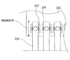
図4は、このようなフレキシブルフィルム配線基板を用いたインクジェット記録ヘッドの一例を示す図である。図4(a)は平面図であり、図4(b)は図4(a)のB−B線に沿う断面図である。 FIG. 4 is a diagram showing an example of an ink jet recording head using such a flexible film wiring board. 4A is a plan view, and FIG. 4B is a cross-sectional view taken along line BB in FIG. 4A.
図4(a)、(b)において、101はシリコン等からなる記録素子基板であり、ウエハの状態から個別にダイシングにより切り出されたものである。102はその内部の電気配線パターンとなるリード端子としてのインナーリード105が形成されたフレキシブルフィルム配線基板である。これらの記録素子基板101及びフレキシブルフィルム配線基板102が支持部材110に高精度に位置決めされて配置されている。フレキシブルフィルム配線基板102には記録素子基板101を固定する長方形のデバイスホール103が形成されている。また、フレキシブルフィルム配線基板102の上面には、ポリイミド等の絶縁性の樹脂からなる平板状のベースフィルム104が形成されている。インナーリード105は、ベースフィルム104の下に銅箔等の導電性材料からなる金属箔を接着し、フォトリソグラフィ技術を用いて所望の形状をパターンニングする事で得られる。パターンニング後のインナーリード105の表面には金や錫やハンダ等のメッキ処理が行なわれ、更に金属面を露出したくない領域にはレジスト層108等により被覆保護される。このとき、配線電極や、本体接続用電極パッド等も形成される。
4A and 4B,
インナーリード105は、フレキシブルフィルム配線基板102からデバイスホール103の開口内に延びて形成されている。記録素子基板101の表面には、複数の電極パッド106が形成されている。電極パッド106は、スタッドバンプ107を介して、デバイスホール103の開口内に延びて存在しているインナーリード105の先端部と電気的に接続されている。
The
電極パッド106には、予め金属により形成されたスタッドバンプ107が配置されて接続される。スタッドバンプ107による端子との接続は、スタッドバンプ107の結合部が溶融され、その後スタッドバンプ107が端子に接触した状態でその結合部が固化して一体化することで行われる。
A
スタッドバンプは、記録素子基板がウエハの状態のときに、記録素子基板の電極パッド上に配置されて結合される。それから、直径数十ミクロンの金ワイヤに放電を行うことで金ワイヤの先端部分をボール状にし、そのボール状にした金ワイヤの先端部分を金ワイヤから離間させることで電極パッド上に配置する。このとき、金ボールにはバンプツールを介して超音波振動が加えられながらスタッドバンプが電極パッド上に配置される。このように、電極パッド上に金ボールが一つずつ形成されるシングルバンプ方式と呼ばれる方式がある。また、これとは別に、電極パッド上にスタッドバンプを形成する方法として、金メッキにより記録素子基板の全ての電極パッド上に一括でバンプを形成するギャングボンディング方式がある。これらの方式によって、スタッドバンプ107が電極パッド上に配置されると、スタッドバンプ107に対応した位置に、これから接続するインナーリード105を位置させる。そして、その状態で支持部材110にフレキシブルフィルム配線基板を接着固定する。その後にインナーリード105の上方よりボンディングツールを用いて、インナーリード105とスタッドバンプ107が接合される。これによりインナーリード105と電極パッド106とが電気的に接続される。通常このような接続方法はILB(Inner Lead Bonding)と呼ばれている。
The stud bump is disposed and bonded on the electrode pad of the recording element substrate when the recording element substrate is in a wafer state. Then, by discharging the gold wire having a diameter of several tens of microns, the tip portion of the gold wire is made into a ball shape, and the tip portion of the gold wire made into the ball shape is placed on the electrode pad by being separated from the gold wire. At this time, stud bumps are arranged on the electrode pads while ultrasonic vibration is applied to the gold balls via the bump tool. Thus, there is a method called a single bump method in which one gold ball is formed on each electrode pad. In addition, as a method of forming stud bumps on electrode pads, there is a gang bonding method in which bumps are collectively formed on all electrode pads of a recording element substrate by gold plating. When the
このように、ILBの方式としては、シングルポイントボンディング方式とギャングボンディング方式との二つの方式が良く知られている。これらのILBの方式は、どちらの方式においてもインナーリード105とスタッドバンプ107との少なくともいずれかが高温に加熱されて溶融された状態で両者の間の接続が行われる。これらの間の接続を、表面が金メッキされたインナーリード105と金のポールから形成されたスタッドバンプ107とを用いてギャングボンディング方式で行う場合には、ボンディングツールの温度は500℃前後まで加熱することが必要とされる。また、これらの間の接続を上述したようなシングルポイントボンディング方式によって行う場合には、ボンディングツールを200℃前後の温度に加熱することが必要とされる。
As described above, two methods, the single point bonding method and the gang bonding method, are well known as ILB methods. In either of these methods, the connection between the
そして、スタッドバンプとインナーリードが一旦加熱されて高温になった後に冷却されて常温に戻されると、高温となることによって一旦膨張した結合部分が冷却されて収縮する。ここで、結合する部材同士で熱膨張係数を比較すると、絶縁性有機樹脂を主体とするベースフィルム104や銅を主体とするインナーリード105の熱膨張係数は、シリコン等からなる記録素子基板101の熱膨張係数に比べてはるかに大きい。従って、加熱した状態で記録素子基板101の電極パッド106上に形成されたスタッドバンプ107とインナーリード105を接続し、その後常温まで冷却されると、冷却後に応力が生じ、その応力が接続部に作用する虞がある。
When the stud bump and the inner lead are once heated to a high temperature and then cooled and returned to room temperature, the joint portion once expanded due to the high temperature is cooled and contracted. Here, when the thermal expansion coefficients of the members to be joined are compared, the thermal expansion coefficient of the
この応力が電極パッド106とスタッドバンプ107との接合強度もしくは、スタッドバンプ107とインナーリード105との接合強度を上回った時には、接合部分に剥がれを生じさせる。すなわち、この応力によりインナーリード105と電極パッド106の接続部の信頼性が低下する虞がある。
When this stress exceeds the bonding strength between the
特に、インクジェット記録ヘッドのような高い位置精度を要求される装置における実装の場合には、記録素子基板101を支持部材110に精度良く固定されることが必要とされている。従って、前述のような残留応力が結合部に残った場合には、それぞれの部材の位置精度を高く保てない虞がある。
In particular, in the case of mounting in an apparatus that requires high positional accuracy such as an ink jet recording head, it is necessary to fix the
このような課題を解決するために、特許文献1には、図5(a)、(b)、(c)に示されるように、インナーリードが変形し易い形状に形成されている記録ヘッドが提案されている。このようにインナーリードが変形し易いような形状に形成されることで、応力が生じたとしてもインナーリードが弾性変形することによってその応力を吸収している。これにより、結合部が加熱されて冷却された際に生じる応力によって結合部の信頼性を低下させ、また、部材の位置精度を低下させることを抑えることができる。 In order to solve such a problem, Patent Document 1 discloses a recording head in which the inner lead is formed in a shape that easily deforms, as shown in FIGS. 5 (a), 5 (b), and 5 (c). Proposed. By forming the inner lead in such a shape that it is easily deformed, even if stress is generated, the inner lead is elastically deformed to absorb the stress. As a result, it is possible to reduce the reliability of the joint portion due to the stress generated when the joint portion is heated and cooled, and to prevent the positional accuracy of the member from being lowered.
しかしながら、特許文献1に開示されている記録ヘッドは、変形を許容する形状とするために、インナーリードの幅を一部小さくし、インナーリードと電極パッドとの接合部以外の領域の断面積を小さくしている。インナーリードの幅を小さくすることでスタッドバンプと電極パッドの接合面以外の領域の断面積を小さくすると、その部分の電気的な抵抗が大きくなる。そのため、記録を行う際にインクジェット記録ヘッドにおける記録素子を駆動させるために通電を行うと、その度にその部分が加熱される。従って、記録が長期間継続して行われた場合、インナーリードに過度の熱が発生する可能性がある。また、加熱された状態でインナーリードが変形を繰り返すので、インナーリードの耐久性が低下する虞がある。このように、インナーリードが変形することにより電気的な接続部での応力が吸収されたとしても、インナーリード自体が変形を繰り返していることから、インナーリードの耐久性が低下する虞が生じる。また、インナーリードの形状が変形し易く複雑になることで、フレキシブルフィルム配線基板を実装する際の工程で、インナーリードを変形させてしまうことも考えられる。さらに、インナーリードの形状が複雑になることで、フレキシブルフィルム配線基板を製造するコストが上昇する虞がある。 However, in the recording head disclosed in Patent Document 1, in order to obtain a shape that allows deformation, the width of the inner lead is partially reduced, and the cross-sectional area of the region other than the joint portion between the inner lead and the electrode pad is reduced. It is small. If the cross-sectional area of the region other than the joint surface between the stud bump and the electrode pad is reduced by reducing the width of the inner lead, the electrical resistance at that portion increases. Therefore, when energization is performed to drive the recording element in the ink jet recording head during recording, the portion is heated each time. Therefore, when recording is performed continuously for a long period of time, excessive heat may be generated in the inner lead. In addition, since the inner lead is repeatedly deformed in a heated state, the durability of the inner lead may be reduced. As described above, even if the stress at the electrical connection portion is absorbed by the deformation of the inner lead, the inner lead itself is repeatedly deformed, which may reduce the durability of the inner lead. In addition, since the shape of the inner lead is easily deformed and complicated, the inner lead may be deformed in the process of mounting the flexible film wiring board. Furthermore, since the shape of the inner lead is complicated, the cost for manufacturing the flexible film wiring board may increase.
さらに、近年ではインクジェット記録装置の小型化が進められている。そのため、記録素子基板の小型化や高集積化が行なわれている。その分電極パッドの大きさが小さくなり、電極パッド間のピッチも狭くなってきている。従って、インナーリードの幅もそれに伴い狭くなってきている。これにより、通電の際にインナーリードに生じる熱がさらに高まる虞がある。 Further, in recent years, miniaturization of ink jet recording apparatuses has been promoted. For this reason, downsizing and higher integration of recording element substrates have been performed. Accordingly, the size of the electrode pads is reduced, and the pitch between the electrode pads is also reduced. Accordingly, the width of the inner lead is becoming narrower accordingly. This may further increase the heat generated in the inner lead when energized.
また、一方で、電極パッドの信頼性の低下について、インナーリードとフレキシブルフィルム配線基板の熱膨張差により発生している以外に、結合部に印加される超音波振動の方向が関係していることが分かっている。 On the other hand, the deterioration of the reliability of the electrode pad is related to the direction of ultrasonic vibration applied to the joint, in addition to the difference in thermal expansion between the inner lead and the flexible film wiring board. I know.
図6(a)には記録素子基板にスタッドバンプを配置して結合させる際に、ウエハ内に複数の記録素子基板が並べられた際のウエハについての平面図が示されている。また、図6(b)には、記録素子基板に形成された電極パッド及びその上に配置されたスタッドバンプの平面図が示されている。図6(c)には、記録素子基板上に配置されたスタッドバンプのC−C線に沿う断面図が示されている。また、図7(a)には、超音波振動の方向が示された記録素子基板の平面図が示されている。また図7(b)には、超音波振動によって上部が平滑化されたスタッドバンプ107のB−B線に沿う断面図が示されている。図8にはスタッドバンプとインナーリードをILBによって接合されている際の平面図が示されている。
FIG. 6A is a plan view of the wafer when a plurality of recording element substrates are arranged in the wafer when the stud bumps are arranged and bonded to the recording element substrate. FIG. 6B shows a plan view of electrode pads formed on the recording element substrate and stud bumps disposed thereon. FIG. 6C shows a cross-sectional view taken along line CC of the stud bump disposed on the recording element substrate. FIG. 7A is a plan view of the recording element substrate showing the direction of ultrasonic vibration. FIG. 7B shows a cross-sectional view along the line BB of the
図6(b)に示されるように、ウエハ内に、パターニングによって複数配置されている記録素子基板の電極パッド106上に、シングルポイント方式でスタッドバンプ107が形成されて接合される。その際、記録素子基板101の長手方向に沿ってスタッドバンプ107に超音波振動が印加される。その後、スタッドバンプ107の頭頂部を平滑化するためのレベリングが行われる。その際にも、図7に示されるように、スタッドバンプ形成時と同様に記録素子基板の長手方向に沿ってスタッドバンプ107に超音波振動が印加される。その後インナーリード105とスタッドバンプ107がILBにより接合される。ILBによるスタッドバンプ107とインナーリード105との間の結合の際にも、図8に示されるように、記録素子基板の長手方向に超音波振動が印加される。
As shown in FIG. 6B, stud bumps 107 are formed and bonded in a single point manner on
これらの工程を経て、記録素子基板101とフレキシブルフィルム配線基板102が電気的に接続される。このときに電気的な接続に用いられる超音波振動は、一般に、全ての工程で記録素子基板101の長手方向に沿って同じ方向に行われる。従って、記録素子基板101に超音波振動による接合後の冷却時に生じる応力と前述の熱膨張差による結合部での応力とが相まって電極パッドに比較的大きな応力が生じる可能性がある。そのため、インナーリードの形状を変形し易い形状とし、これによって冷却時に残った応力を吸収することとしても、超音波振動による接続の後に生じる応力によって吸収可能な分の応力を上回り記録ヘッドの信頼性を低下させる虞がある。
Through these steps, the
本発明は上記の問題点に鑑みてなされたものであり、記録素子基板側の電極端子とリード端子との間の結合部が一旦加熱されて冷却された際に応力が生じても、結合部での信頼性の低下が抑えられる記録ヘッドを提供することを目的とする。 The present invention has been made in view of the above problems, and even if a stress occurs when the joint between the electrode terminal on the recording element substrate side and the lead terminal is once heated and cooled, the joint An object of the present invention is to provide a recording head in which a decrease in reliability is suppressed.
本発明の記録ヘッドによれば、吐出口から液体を吐出するために当該液体にエネルギーを付与する記録素子と、前記記録素子に電気エネルギーを伝送するために前記記録素子から延びている配線の端部に形成されている電極端子と、前記記録素子を駆動させるための駆動信号の伝送を行うために前記電極端子に対応して配置されたリード端子とを有する記録ヘッドにおいて、前記電極端子と前記リード端子とがバンプを介して接続されており、前記電極端子と前記バンプとの間の接続は、前記電極端子と前記バンプとが接触した状態で超音波振動が接続部に第一の方向に印加されることで行われ、前記リード端子と前記バンプとの間の接続は、前記リード端子と前記バンプとが接触した状態で超音波振動が接続部に前記第一の方向に交差する第二の方向に印加されることで行われることを特徴とする。 According to the recording head of the present invention, a recording element that imparts energy to the liquid in order to discharge the liquid from the discharge port, and an end of a wiring that extends from the recording element to transmit electric energy to the recording element In a recording head having an electrode terminal formed in a portion, and a lead terminal arranged corresponding to the electrode terminal to transmit a drive signal for driving the recording element, the electrode terminal and the A lead terminal is connected via a bump, and the connection between the electrode terminal and the bump is such that ultrasonic vibration is applied to the connection portion in a first direction while the electrode terminal and the bump are in contact with each other. The connection between the lead terminal and the bump is performed by applying the ultrasonic vibration to the connection portion in the first direction in a state where the lead terminal and the bump are in contact with each other. Characterized in that it is carried out by being applied to the second direction.
また、本発明の記録ヘッドの製造方法によれば、吐出口から液体を吐出するために当該液体にエネルギーを付与する記録素子と、前記記録素子に電気エネルギーを伝送するために前記記録素子から延びている配線の端部に形成されている電極端子と、前記記録素子を駆動させるための駆動信号の伝送を行うために前記電極端子に対応して配置されたリード端子とを有し、前記電極端子と前記リード端子とがバンプを介して接続された記録ヘッドを製造する記録ヘッドの製造方法において、前記電極端子と前記バンプとが接触した状態で超音波振動を接続部に第一の方向に印加して前記電極端子と前記バンプとの間の接続を行う電極端子接続工程と、前記リード端子と前記バンプとが接触した状態で超音波振動を接続部に前記第一の方向に交差する第二の方向に印加して前記リード端子と前記バンプとの間の接続を行うリード端子接続工程とを具えることを特徴とする。 According to the recording head manufacturing method of the present invention, a recording element that imparts energy to the liquid in order to discharge the liquid from the discharge port, and an extension from the recording element to transmit electric energy to the recording element. An electrode terminal formed at an end portion of the wiring, and a lead terminal arranged corresponding to the electrode terminal for transmitting a drive signal for driving the recording element, and the electrode In a recording head manufacturing method for manufacturing a recording head in which a terminal and the lead terminal are connected via a bump, ultrasonic vibration is applied to the connecting portion in a first direction in a state where the electrode terminal and the bump are in contact with each other. An electrode terminal connection step of applying and connecting between the electrode terminal and the bump, and crossing the ultrasonic vibration in the first direction at the connection portion in a state where the lead terminal and the bump are in contact with each other. Is applied in a second direction, characterized in that it comprises a lead terminal connecting step for connecting between the lead terminals and the bumps that.
本発明によれば、記録素子基板側の電極端子とリード端子との間の結合部での信頼性が向上されるので、結果的に信頼性の向上された記録ヘッドを提供することができる。 According to the present invention, the reliability at the joint between the electrode terminal on the recording element substrate side and the lead terminal is improved, and as a result, a recording head with improved reliability can be provided.
以下、本発明を実施するための実施形態について添付図面を参照しながら説明する。 Embodiments for carrying out the present invention will be described below with reference to the accompanying drawings.
本実施形態の記録ヘッドは、インクジェット記録装置に適用され、記録媒体に対して液体としてのインクを吐出する。この記録ヘッドの構成について図1を参照して説明する。この記録ヘッドは、液室に貯留されるインクを吐出するためにインクにエネルギーを付与する記録素子203が設けられた記録素子基板101と、この記録素子基板101に接合されるオリフィスプレート201とを備えている。オリフィスプレート201は、インクとしての液滴を吐出する複数の吐出口202を有している。また、オリフィスプレート201が記録素子基板101に接合されることによって吐出口202が連通するエネルギー作用室として内部にインクを貯留可能な液室204及びこれに連通するインク流路等が形成される。液室204の内部空間を画成する壁のうち記録素子基板101の内部には、記録素子203が埋設されている。そして、記録素子203の駆動によって液室204の内部で気泡を発生させ、その発泡圧によって吐出口202から液室204に貯留されるインクが吐出される。また、記録素子基板101には、オリフィスプレート201に接する主面からその反対側の裏面にかけて記録素子基板101を貫通するようにインク供給口205が形成されている。
The recording head of this embodiment is applied to an ink jet recording apparatus, and ejects ink as a liquid to a recording medium. The configuration of this recording head will be described with reference to FIG. The recording head includes a
図2に示されるように、記録素子基板101には、インクを吐出するための電気エネルギーを伝送するために記録素子203から延びている配線の端部に形成されている電極端子としての電極パッド106が形成されている。また、電極パッド106に対応した位置には、記録素子203を駆動させるための駆動信号の伝送を行うために配置されたリード端子としてのインナーリード105が形成されている。本実施形態では、電極パッド106とインナーリード105とがバンプとしてのスタッドバンプ107を介して接続されている。
As shown in FIG. 2, an electrode pad as an electrode terminal formed on an end portion of a wiring extending from the
本実施形態の記録ヘッドの製造方法について図2(a)、(b)、(c)に基づいて説明する。図2(a)は本実施形態のスタッドバンプ107が電極パッド106に結合される際の記録素子基板101を示す平面図である。図2(b)は、スタッドバンプ107の頭頂部を平滑化するレベリングが行われた後の、スタッドバンプ107及び記録素子基板101を示す平面図である。図2(c)は、スタッドバンプ107とインナーリード105とをILBによって接合する際の電極パッド106とインナーリード105との接合部を示す平面図である。
A method for manufacturing the recording head of this embodiment will be described with reference to FIGS. 2 (a), 2 (b), and 2 (c). FIG. 2A is a plan view showing the
本実施形態では、まず、複数の記録素子基板101がウエハ内に形成されている段階で電極パッド106とスタッドバンプ107との接続が行われる(電極端子接続工程)。本実施形態では、電極端子接続工程では、電極パッド106がウエハ内に形成されている。ウエハ内に複数パターニングにより配置された記録素子基板101の電極パッド106に、シングルポイント方式でスタッドバンプ107を形成し接続する。その際に、ウエハ内の全ての領域で図2(a)の矢印で示す通り、振動方向を記録素子基板101の長手方向に対し60度の角度を付けた状態で超音波振動を結合部に印加する。このように、電極端子接続工程としての電極パッド接続工程で、電極パッド106とスタッドバンプ107とが接触した状態で超音波振動を接続部へ第一の方向に印加して電極パッド106とスタッドバンプ107との間の接続を行う。
In the present embodiment, first, the
本実施形態では、電極パッド接続工程でスタッドバンプ107が電極パッド106に接続されるのは、電極パッド106がウエハ内に形成されている段階である。そして、ウエハ内の全ての電極パッド106とスタッドバンプ107との間の接続部に対して超音波振動が第一の方向に印加される。本実施形態では、このようにウエハ内の全ての記録素子基板101について一括して電極パッド106とスタッドバンプ107との接続が行われるので、記録ヘッドの製造工程が短縮化される。
In the present embodiment, the
次に、本実施形態では後述するバンプ形成工程が行われる。バンプ形成工程が行われている際のスタッドバンプ107と電極パッド106との結合部についての平面図を図2(b)に示す。
Next, in the present embodiment, a bump forming process described later is performed. FIG. 2B shows a plan view of the joint portion between the
その後、スタッドバンプ107が形成された記録素子基板101が、ダイシングにより個別に切り出される。そして取り出された記録素子基板101が、支持部材に対して高精度に位置決めが行われて配置される。
Thereafter, the
そして次に、リード端子接続工程としてのインナーリード接続工程で、インナーリード105とスタッドバンプ107とが接触した状態で接続部に超音波振動を第二の方向に印加してインナーリード105とスタッドバンプ107との間の接続を行う。ここで、第二の方向は、第一の方向に交差する方向である。このとき、図2(c)に示されるように、インナーリード105の上方よりボンディングツールを用いて、インナーリード105とスタッドバンプ107をILBで接合させる。ILB時の超音波振動方向は、図2(c)の矢印で示す通り記録素子基板101の長手方向とする。このとき、フレキシブルフィルム配線基板102におけるインナーリード105の中心が記録素子基板101の電極パッド中心と重なるような位置で、フレキシブルフィルム配線基板102と記録素子基板101とが接合される。
Next, in the inner lead connecting step as the lead terminal connecting step, the
ここで、電極端子接続工程とインナーリード接続工程との間のバンプ形成工程について説明する。本実施形態では、電極端子接続工程でスタッドバンプ107が電極パッド106に接続された後にスタッドバンプ107の頭頂部を平滑化するために超音波振動と荷重をスタッドバンプ107に与えてレベリングを行なう。このように、スタッドバンプ107は、超音波振動が印加されて所定の形状に形成される。そして、スタッドバンプ107を所定の形状とするために印加される超音波振動は、第一の方向及び第二の方向に交差する第三の方向に印加される。このとき、ウエハ内の全ての領域で図2(b)の矢印で示す方向に、超音波振動が行われる。すなわち、本実施形態では、超音波振動は、記録素子基板101の長手方向に対し120度傾けた方向に行われる。これにより、ウエハ内の全ての領域で、スタッドバンプ107と電極パッド106との間の接続時における超音波振動と、レベリングの際の超音波振動の方向が交差する。このように、電極端子接続工程の後のバンプ形成工程で、電極パッド106に接続されたスタッドバンプ107に、第一の方向及び第二の方向に交差する第三の方向に超音波振動を印加してスタッドバンプ107を所定の形状に形成する。
Here, a bump forming process between the electrode terminal connecting process and the inner lead connecting process will be described. In the present embodiment, after the
本実施形態では、記録素子基板101の長手方向に沿った方向を基準とすると、第一の方向は、基準とした記録素子基板101の長手方向から60度傾いた方向である(図2(a))。また、第三の方向は、第一の方向から基準の方向に対してさらに60度傾いた方向である(図2(b))。また、第二の方向は、第三の方向から基準の方向に対してさらに60度傾いた方向である(図2(c))。
In this embodiment, when the direction along the longitudinal direction of the
これにより、本実施形態では、スタッドバンプと電極パッドとの接続・スタッドバンプのレベリング・ILBと三回の超音波振動をスタッドバンプ107及び結合部に対して印加する。その際に、三回の超音波振動の方向はそれぞれ60°の角度を持って交差するので、応力の生じる方向が集中せずに交差する。従って、それぞれの工程で生じた応力の方向が分散される。それに伴い応力が集中することが抑えられて記録ヘッドの信頼性が向上する。
Thereby, in this embodiment, the connection between the stud bump and the electrode pad, the leveling of the stud bump, the ILB, and the three times of ultrasonic vibration are applied to the
本実施形態における記録ヘッドは、上記のように記録素子基板101の電極パッド106とフレキシブルフィルム配線基板102のインナーリード105とが接続されて製造される。従って、本実施形態の記録ヘッドは、電極パッド106とインナーリード105とがスタッドバンプ107を介して接続されている。そして、電極パッド106とスタッドバンプ107との間の接続は、電極パッド106とスタッドバンプ107とが接触した状態で超音波振動が接続部に第一の方向に印加されることで行われている。そして、インナーリード105とスタッドバンプ107との間の接続は、インナーリード105とスタッドバンプ107とが接触した状態で超音波振動が接続部に第一の方向に交差する第二の方向に印加されることで行われている。
The recording head in this embodiment is manufactured by connecting the
また、記録ヘッドの製造の際には、スタッドバンプ107は、超音波振動が印加されて所定の形状に形成される。そして、スタッドバンプ107を所定の形状とするために印加される超音波振動は、第一の方向及び第二の方向に交差する第三の方向に印加されて行われている。
Further, when the recording head is manufactured, the
図3は、通常用いられている超音波出力よりも高い値の設定による超音波出力で超音波振動が印加されてILBを行なった後に、インナーリードを引っ張り上げ、クレタリングの発生率を確認した際の比較結果である。ここで、クレタリングは、電極パッドとインナーリードとの間で電気的な接続が行われている部分で生じる破壊のことをいうものとする。この試験は、無負荷の状態からインナーリードを引っ張り上げる力を徐々に増加させ、電極パッドとインナーリードとの間の電気的な接続が分断されるまで行われる。そして、そのときに電極パッド、スタッドバンプ及びインナーリードの間の接続部分が破壊されている場合にはクレタリングが発生したものとする。これに対して、これらの間の接続部分以外の部分が破壊されたとき、例えば、インナーリードにおける接続部分以外の部分等が破壊されている場合には、クレタリングは発生していないものとする。図3のテーブルでは、本実施形態における電極パッドとインナーリードとの電気的な接続が行われた場合と、従来方式による接続が行われた場合とで、プル試験が行われた際のクレタリングの発生率を比較している。 FIG. 3 shows the occurrence rate of cretering by pulling up the inner lead after performing the ILB by applying ultrasonic vibration with an ultrasonic output set to a value higher than that of a normal ultrasonic output. It is a comparison result. Here, cretering refers to destruction that occurs at a portion where electrical connection is made between the electrode pad and the inner lead. This test is performed until the electric connection between the electrode pad and the inner lead is broken by gradually increasing the pulling force of the inner lead from the unloaded state. Then, if the connection portion between the electrode pad, stud bump, and inner lead is broken at that time, it is assumed that cretering has occurred. On the other hand, when a part other than the connection part between them is destroyed, for example, when a part other than the connection part in the inner lead is destroyed, no cretering occurs. . In the table of FIG. 3, the cretering when the pull test is performed between the case where the electrode pad and the inner lead in the present embodiment are electrically connected and the case where the connection according to the conventional method is made. The incidence rate is compared.
通常よりも強い超音波出力でILBが行われた場合、通常の超音波振動が印加される場合よりも大きな応力が残ると考えられるが、本実施形態のように超音波振動を印加する方向を一回ごとに変えることで、応力のかかる方向が分散される。従って、本実施形態の記録ヘッドでは、通常よりも強い超音波出力でILBが行われた場合であっても、この条件では、従来の方式の記録ヘッドと比較して約半分のクレタリングの発生率に抑えることが可能となっている。 When ILB is performed with an ultrasonic output stronger than normal, it is considered that a larger stress remains than when normal ultrasonic vibration is applied. However, the direction in which ultrasonic vibration is applied is changed as in this embodiment. By changing each time, the direction in which the stress is applied is dispersed. Therefore, in the recording head of this embodiment, even when ILB is performed with an ultrasonic output stronger than usual, under this condition, about half of the cretering occurs as compared with the conventional recording head. It is possible to limit to the rate.
なお、本発明の記録ヘッドは、プリンタ、複写機、通信システムを有するファクシミリ、プリンタ部を有するワードプロセッサなどの装置、さらには各種処理装置と複合的に組み合わせた産業記録装置に搭載可能である。そして、この記録ヘッドを用いることによって、紙、糸、繊維、布帛、皮革、金属、プラスチック、ガラス、木材、セラミックスなど種々の記録媒体に記録を行うことができる。なお、本明細書内で用いられる「記録」とは、文字や図形などの意味を持つ画像を記録媒体に対して付与することだけでなく、パターンなどの意味を持たない画像を付与することも意味することとする。 The recording head of the present invention can be mounted on an apparatus such as a printer, a copying machine, a facsimile having a communication system, a word processor having a printer unit, or an industrial recording apparatus combined with various processing apparatuses. By using this recording head, recording can be performed on various recording media such as paper, thread, fiber, fabric, leather, metal, plastic, glass, wood, and ceramics. Note that “recording” used in the present specification not only applies an image having a meaning such as a character or a figure to a recording medium but also an image having no meaning such as a pattern. I mean.
101 記録素子基板
105 インナーリード
106 電極パッド
107 スタッドバンプ
202 吐出口
203 記録素子
204 液室
101
Claims (5)
前記記録素子に電気エネルギーを伝送するために前記記録素子から延びている配線の端部に形成されている電極端子と、
前記記録素子を駆動させるための駆動信号の伝送を行うために前記電極端子に対応して配置されたリード端子と
を有する記録ヘッドにおいて、
前記電極端子と前記リード端子とがバンプを介して接続されており、
前記電極端子と前記バンプとの間の接続は、前記電極端子と前記バンプとが接触した状態で超音波振動が接続部に第一の方向に印加されることで行われ、
前記リード端子と前記バンプとの間の接続は、前記リード端子と前記バンプとが接触した状態で超音波振動が接続部に前記第一の方向に交差する第二の方向に印加されることで行われることを特徴とする記録ヘッド。 A recording element for applying energy to the liquid in order to discharge the liquid from the discharge port;
An electrode terminal formed at an end of a wiring extending from the recording element to transmit electric energy to the recording element;
In a recording head having a lead terminal arranged corresponding to the electrode terminal for transmitting a drive signal for driving the recording element,
The electrode terminal and the lead terminal are connected via a bump,
The connection between the electrode terminal and the bump is performed by applying ultrasonic vibration in a first direction to the connection portion in a state where the electrode terminal and the bump are in contact with each other,
The connection between the lead terminal and the bump is such that ultrasonic vibration is applied to the connection portion in a second direction intersecting the first direction in a state where the lead terminal and the bump are in contact with each other. A recording head characterized by being performed.
前記バンプを所定の形状とするために印加される超音波振動は、前記第一の方向及び前記第二の方向に交差する第三の方向に印加されることで行われることを特徴とする請求項1に記載の記録ヘッド。 The bump is formed in a predetermined shape by applying ultrasonic vibration,
The ultrasonic vibration applied to make the bump a predetermined shape is performed by being applied in a third direction that intersects the first direction and the second direction. Item 2. The recording head according to Item 1.
前記記録素子に電気エネルギーを伝送するために前記記録素子から延びている配線の端部に形成されている電極端子と、
前記記録素子を駆動させるための駆動信号の伝送を行うために前記電極端子に対応して配置されたリード端子とを有し、
前記電極端子と前記リード端子とがバンプを介して接続された記録ヘッドを製造する記録ヘッドの製造方法において、
前記電極端子と前記バンプとが接触した状態で超音波振動を接続部に第一の方向に印加して前記電極端子と前記バンプとの間の接続を行う電極端子接続工程と、
前記リード端子と前記バンプとが接触した状態で超音波振動を接続部に前記第一の方向に交差する第二の方向に印加して前記リード端子と前記バンプとの間の接続を行うリード端子接続工程と
を具えることを特徴とする記録ヘッドの製造方法。 A recording element for applying energy to the liquid in order to discharge the liquid from the discharge port;
An electrode terminal formed at an end of a wiring extending from the recording element to transmit electric energy to the recording element;
A lead terminal arranged corresponding to the electrode terminal for transmitting a drive signal for driving the recording element;
In a manufacturing method of a recording head for manufacturing a recording head in which the electrode terminal and the lead terminal are connected via a bump,
An electrode terminal connection step of applying ultrasonic vibration in a first direction to a connection portion in a state where the electrode terminal and the bump are in contact with each other to connect the electrode terminal and the bump;
A lead terminal for applying a connection between the lead terminal and the bump by applying ultrasonic vibration to the connecting portion in a second direction intersecting the first direction in a state where the lead terminal and the bump are in contact with each other. A recording head manufacturing method comprising: a connecting step.
所定の形状に形成されたバンプが前記リード端子接続工程で前記リード端子に接続されることを特徴とする請求項3に記載の記録ヘッドの製造方法。 After the electrode terminal connecting step, ultrasonic vibration is applied to the bumps connected to the electrode terminals in a third direction intersecting the first direction and the second direction so that the bumps have a predetermined shape. The bump formation process to form in
4. The method of manufacturing a recording head according to claim 3, wherein the bump formed in a predetermined shape is connected to the lead terminal in the lead terminal connecting step.
前記バンプが前記電極端子に接続されるのは、前記電極端子がウエハ内に形成されている段階であり、
前記ウエハ内の全ての前記電極端子と前記バンプとの間の接続部に対して超音波振動が第一の方向に印加されることを特徴とする請求項3または4に記載の記録ヘッドの製造方法。 In the electrode terminal connection step, the electrode terminal is formed in the wafer,
The bumps are connected to the electrode terminals when the electrode terminals are formed in the wafer,
5. The recording head according to claim 3, wherein ultrasonic vibration is applied in a first direction to connection portions between all the electrode terminals and the bumps in the wafer. Method.
Priority Applications (2)
| Application Number | Priority Date | Filing Date | Title |
|---|---|---|---|
| JP2008161810A JP5173624B2 (en) | 2008-06-20 | 2008-06-20 | Recording head and manufacturing method of recording head |
| US12/485,257 US8210652B2 (en) | 2008-06-20 | 2009-06-16 | Printing head and method of manufacturing printing head |
Applications Claiming Priority (1)
| Application Number | Priority Date | Filing Date | Title |
|---|---|---|---|
| JP2008161810A JP5173624B2 (en) | 2008-06-20 | 2008-06-20 | Recording head and manufacturing method of recording head |
Publications (2)
| Publication Number | Publication Date |
|---|---|
| JP2010000704A true JP2010000704A (en) | 2010-01-07 |
| JP5173624B2 JP5173624B2 (en) | 2013-04-03 |
Family
ID=41430789
Family Applications (1)
| Application Number | Title | Priority Date | Filing Date |
|---|---|---|---|
| JP2008161810A Active JP5173624B2 (en) | 2008-06-20 | 2008-06-20 | Recording head and manufacturing method of recording head |
Country Status (2)
| Country | Link |
|---|---|
| US (1) | US8210652B2 (en) |
| JP (1) | JP5173624B2 (en) |
Cited By (3)
| Publication number | Priority date | Publication date | Assignee | Title |
|---|---|---|---|---|
| CN102233732A (en) * | 2010-04-15 | 2011-11-09 | 佳能株式会社 | Liquid discharge head and method for manufacturing the same |
| JP2012152984A (en) * | 2011-01-25 | 2012-08-16 | Canon Inc | Liquid ejection head and method of manufacturing the same |
| JP2020527485A (en) * | 2017-07-26 | 2020-09-10 | ヒューレット−パッカード デベロップメント カンパニー エル.ピー.Hewlett‐Packard Development Company, L.P. | Die contact formation |
Families Citing this family (2)
| Publication number | Priority date | Publication date | Assignee | Title |
|---|---|---|---|---|
| US8767351B1 (en) * | 2013-01-31 | 2014-07-01 | Seagate Technology Llc | Ambient temperature ball bond |
| TWI814839B (en) * | 2018-07-30 | 2023-09-11 | 瑞士商西克帕控股有限公司 | A multi-chip module (mcm) assembly and a printing bar |
Citations (8)
| Publication number | Priority date | Publication date | Assignee | Title |
|---|---|---|---|---|
| JPH0799219A (en) * | 1993-09-29 | 1995-04-11 | Nec Kansai Ltd | Method and system for manufacturing semiconductor device |
| JPH1197493A (en) * | 1997-09-19 | 1999-04-09 | Toshiba Corp | Bonding method and device |
| JPH11284028A (en) * | 1998-03-27 | 1999-10-15 | Toshiba Corp | Bonding method and its device |
| JP2000021917A (en) * | 1998-07-02 | 2000-01-21 | Sanyo Electric Co Ltd | Method for forming bump contact point |
| JP2002154208A (en) * | 2000-07-10 | 2002-05-28 | Canon Inc | Ink jet recording head and recorder |
| JP2002252253A (en) * | 2001-02-23 | 2002-09-06 | Matsushita Electric Ind Co Ltd | Method and apparatus for jointing component |
| JP2003347336A (en) * | 2002-05-24 | 2003-12-05 | Murata Mfg Co Ltd | Mounting method of electronic component |
| JP2005159372A (en) * | 2005-01-28 | 2005-06-16 | Seiko Epson Corp | Bump structure and manufacturing method of bump |
Family Cites Families (5)
| Publication number | Priority date | Publication date | Assignee | Title |
|---|---|---|---|---|
| JP2631013B2 (en) * | 1989-04-17 | 1997-07-16 | 株式会社新川 | Bump forming method |
| JPH10230611A (en) * | 1997-02-19 | 1998-09-02 | Canon Inc | Liquid ejection recording head and manufacture thereof |
| EP1172215B1 (en) * | 2000-07-10 | 2017-09-20 | Canon Kabushiki Kaisha | Ink jet recording head and recording apparatus |
| JP4393303B2 (en) | 2003-09-05 | 2010-01-06 | キヤノン株式会社 | Manufacturing method of semiconductor device |
| JP4290154B2 (en) * | 2004-12-08 | 2009-07-01 | キヤノン株式会社 | Liquid discharge recording head and ink jet recording apparatus |
-
2008
- 2008-06-20 JP JP2008161810A patent/JP5173624B2/en active Active
-
2009
- 2009-06-16 US US12/485,257 patent/US8210652B2/en active Active
Patent Citations (8)
| Publication number | Priority date | Publication date | Assignee | Title |
|---|---|---|---|---|
| JPH0799219A (en) * | 1993-09-29 | 1995-04-11 | Nec Kansai Ltd | Method and system for manufacturing semiconductor device |
| JPH1197493A (en) * | 1997-09-19 | 1999-04-09 | Toshiba Corp | Bonding method and device |
| JPH11284028A (en) * | 1998-03-27 | 1999-10-15 | Toshiba Corp | Bonding method and its device |
| JP2000021917A (en) * | 1998-07-02 | 2000-01-21 | Sanyo Electric Co Ltd | Method for forming bump contact point |
| JP2002154208A (en) * | 2000-07-10 | 2002-05-28 | Canon Inc | Ink jet recording head and recorder |
| JP2002252253A (en) * | 2001-02-23 | 2002-09-06 | Matsushita Electric Ind Co Ltd | Method and apparatus for jointing component |
| JP2003347336A (en) * | 2002-05-24 | 2003-12-05 | Murata Mfg Co Ltd | Mounting method of electronic component |
| JP2005159372A (en) * | 2005-01-28 | 2005-06-16 | Seiko Epson Corp | Bump structure and manufacturing method of bump |
Cited By (5)
| Publication number | Priority date | Publication date | Assignee | Title |
|---|---|---|---|---|
| CN102233732A (en) * | 2010-04-15 | 2011-11-09 | 佳能株式会社 | Liquid discharge head and method for manufacturing the same |
| JP2012152984A (en) * | 2011-01-25 | 2012-08-16 | Canon Inc | Liquid ejection head and method of manufacturing the same |
| JP2020527485A (en) * | 2017-07-26 | 2020-09-10 | ヒューレット−パッカード デベロップメント カンパニー エル.ピー.Hewlett‐Packard Development Company, L.P. | Die contact formation |
| US11135839B2 (en) | 2017-07-26 | 2021-10-05 | Hewlett-Packard Development Company, L.P. | Die contact formations |
| JP7053786B2 (en) | 2017-07-26 | 2022-04-12 | ヒューレット-パッカード デベロップメント カンパニー エル.ピー. | Die contact formation |
Also Published As
| Publication number | Publication date |
|---|---|
| US8210652B2 (en) | 2012-07-03 |
| JP5173624B2 (en) | 2013-04-03 |
| US20090315947A1 (en) | 2009-12-24 |
Similar Documents
| Publication | Publication Date | Title |
|---|---|---|
| US7390079B2 (en) | Device mounting structure, device mounting method, electronic apparatus, liquid droplet ejection head, and liquid droplet ejection apparatus | |
| JP5975030B2 (en) | Inkjet head manufacturing method and inkjet drawing apparatus manufacturing method | |
| JP5173624B2 (en) | Recording head and manufacturing method of recording head | |
| US7954690B2 (en) | Inkjet print head, inkjet print head manufacturing method and inkjet print head mounting tool | |
| JP4393303B2 (en) | Manufacturing method of semiconductor device | |
| US8746849B2 (en) | Liquid discharge head and method for manufacturing the same | |
| JP3459726B2 (en) | Ink jet recording head and method of manufacturing the same | |
| JP3972639B2 (en) | Method for joining components of inkjet head | |
| JP2009298118A (en) | Recording head, and manufacturing method for recording head | |
| JP4687410B2 (en) | Device mounting structure and droplet discharge head | |
| JP5147382B2 (en) | SEMICONDUCTOR ELEMENT SUBSTRATE, INK JET HEAD USING THE ELEMENT SUBSTRATE, AND SEMICONDUCTOR ELEMENT SUBSTRATE ELECTROCONNECTION METHOD | |
| JP2004074740A (en) | Liquid jetting head member | |
| JP4403955B2 (en) | Wire bonding method | |
| JP7309449B2 (en) | Semiconductor element, method for manufacturing semiconductor element, and liquid ejection head | |
| JP2005041158A (en) | Inkjet recoding head chip | |
| JP2005197488A (en) | Projection electrode, bonding capillary and semiconductor chip | |
| JP2006121045A (en) | Bonding structure, actuator equipment, and liquid injection head | |
| JP2010041061A (en) | Liquid jet head | |
| JP7309518B2 (en) | inkjet recording head | |
| JP2010240851A (en) | Liquid droplet ejection head, method for manufacturing the liquid droplet ejection head, and liquid droplet ejection device | |
| JP2008143132A (en) | Inkjet recording head | |
| JP2007083401A (en) | Manufacturing method for wiring substrate, and liquid delivering head | |
| JP2005219238A (en) | Inkjet recording head, its manufacturing method, and inkjet recording apparatus | |
| JPH07285219A (en) | Ink jet head | |
| JP2004262190A (en) | Electrical connection structure, ink jet recording head using the same, and recording device |
Legal Events
| Date | Code | Title | Description |
|---|---|---|---|
| RD02 | Notification of acceptance of power of attorney |
Free format text: JAPANESE INTERMEDIATE CODE: A7422 Effective date: 20101106 |
|
| A621 | Written request for application examination |
Free format text: JAPANESE INTERMEDIATE CODE: A621 Effective date: 20110606 |
|
| A977 | Report on retrieval |
Free format text: JAPANESE INTERMEDIATE CODE: A971007 Effective date: 20121128 |
|
| TRDD | Decision of grant or rejection written | ||
| A01 | Written decision to grant a patent or to grant a registration (utility model) |
Free format text: JAPANESE INTERMEDIATE CODE: A01 Effective date: 20121204 |
|
| A61 | First payment of annual fees (during grant procedure) |
Free format text: JAPANESE INTERMEDIATE CODE: A61 Effective date: 20121227 |
|
| R151 | Written notification of patent or utility model registration |
Ref document number: 5173624 Country of ref document: JP Free format text: JAPANESE INTERMEDIATE CODE: R151 |
|
| FPAY | Renewal fee payment (event date is renewal date of database) |
Free format text: PAYMENT UNTIL: 20160111 Year of fee payment: 3 |