EP3196995B1 - Bandmaterial mit kaschierter struktur zur herstellung einer zündkerzenelektrode - Google Patents
Bandmaterial mit kaschierter struktur zur herstellung einer zündkerzenelektrode Download PDFInfo
- Publication number
- EP3196995B1 EP3196995B1 EP15841466.4A EP15841466A EP3196995B1 EP 3196995 B1 EP3196995 B1 EP 3196995B1 EP 15841466 A EP15841466 A EP 15841466A EP 3196995 B1 EP3196995 B1 EP 3196995B1
- Authority
- EP
- European Patent Office
- Prior art keywords
- metal layer
- electrode
- tape material
- tape
- ignition plug
- Prior art date
- Legal status (The legal status is an assumption and is not a legal conclusion. Google has not performed a legal analysis and makes no representation as to the accuracy of the status listed.)
- Active
Links
Images


Classifications
-
- H—ELECTRICITY
- H01—ELECTRIC ELEMENTS
- H01T—SPARK GAPS; OVERVOLTAGE ARRESTERS USING SPARK GAPS; SPARKING PLUGS; CORONA DEVICES; GENERATING IONS TO BE INTRODUCED INTO NON-ENCLOSED GASES
- H01T13/00—Sparking plugs
- H01T13/20—Sparking plugs characterised by features of the electrodes or insulation
- H01T13/39—Selection of materials for electrodes
-
- B—PERFORMING OPERATIONS; TRANSPORTING
- B23—MACHINE TOOLS; METAL-WORKING NOT OTHERWISE PROVIDED FOR
- B23K—SOLDERING OR UNSOLDERING; WELDING; CLADDING OR PLATING BY SOLDERING OR WELDING; CUTTING BY APPLYING HEAT LOCALLY, e.g. FLAME CUTTING; WORKING BY LASER BEAM
- B23K11/00—Resistance welding; Severing by resistance heating
- B23K11/002—Resistance welding; Severing by resistance heating specially adapted for particular articles or work
-
- H—ELECTRICITY
- H01—ELECTRIC ELEMENTS
- H01T—SPARK GAPS; OVERVOLTAGE ARRESTERS USING SPARK GAPS; SPARKING PLUGS; CORONA DEVICES; GENERATING IONS TO BE INTRODUCED INTO NON-ENCLOSED GASES
- H01T21/00—Apparatus or processes specially adapted for the manufacture or maintenance of spark gaps or sparking plugs
- H01T21/02—Apparatus or processes specially adapted for the manufacture or maintenance of spark gaps or sparking plugs of sparking plugs
Definitions
- the present invention relates to a tape material which is used as a member for forming an ignition plug electrode (center electrode or earth electrode) and which has a clad structure.
- the present invention relates to a clad tape material including a precious metal layer and a base metal layer, where the base metal layer is bonded to an ignition plug, and the precious metal layer serves as an electrode surface.
- Precious metals and alloys of the precious metals are used in ignition plug electrodes (center electrodes and earth electrodes) to be used in internal combustion engines.
- ignition plug electrodes center electrodes and earth electrodes
- a chip-shaped precious metal material has been commonly bonded to a base material including a heat-resistant material such as a Ni alloy on the ignition plug side.
- laser welding is known and described e.g. in US 2004/092193 A1 .
- the outer peripheral surface of a part at which a precious metal chip and a base material are in contact with each other is irradiated with a laser beam to melt the irradiated part, so that the precious metal chip and the base material are bonded to each other.
- Laser welding melts the outer peripheral surface of a bonded part between a precious metal chip and a base material, but a part inside the bonded surface may be unmelted.
- a void may remain at the bonded interface, and when the temperature is elevated during use, a gas in the void is expanded, so that cracks tend to be generated, leading to separation of the precious metal chip from the base material.
- a molten zone is generated on the outer peripheral surface of a bonded part.
- the molten zone is a region formed by melting/solidification of a material.
- the molten zone is different in composition of the material and structures from a precious metal parent material, and is fragile and poor in electrical properties. In other words, the molten zone is not a portion that is effective as a plug material.
- the precious metal chip is required to have an excessive length, which is not preferable from the viewpoint of a cost based on the use amount of a precious metal, or resource saving.
- documents US 2014/0265813 A1 and CN 103094842 A describe resistance welding of a metal chip to an electrode base material of a spark plug.
- GB 2068814 A and JP 2009302066 A describe projection-welding of a metal substrate carrying at least one spot-like projection on the surface to be welded.
- the present inventors recommend application of an electrode chip formed from a precious metal layer and a substrate and having a clad structure in place of a conventional metal chip including a precious metal.
- the electrode chip for a plug electrode is formed by bonding a thin precious metal layer to a substrate including, for example, Ni or a Ni alloy by diffusive bonding under controlled bonding conditions.
- the electrode chip contributes to reduction of the use amount of a precious metal because a precious metal layer and a substrate are bonded to each other with optimum bonding conditions determined beforehand, so that the thickness of the precious metal layer can be minimized while the electrode characteristics and life are secured. Further, bonding for mounting of a chip can be facilitated because a Ni alloy etc. that is identical to a base material for the plug electrode is used as the substrate.
- Formation of a plug electrode by use of an electrode chip by the present inventors has the above-mentioned advantages, but is required to be further improved. Particularly, improvement production efficiency associated with handling characteristics of an electrode chip is pointed out.
- an electrode chip In production of a plug, an electrode chip is positioned and placed on a surface of a base material of a fixed plug body, and bonding is then performed to form an electrode part. This operation is complicated because electrode chips are handled one by one. This improvement request is also pointed out for conventional precious metal chips, but efficiency is hardly improved.
- the present invention provides a member and process for efficiently forming a plug electrode having a clad structure in which a thin precious metal layer is combined with a substrate while making use of the form of the clad structure.
- the present invention provides a tape material according to claim 1 (whose preferred embodiments are defined in dependent claims) and a method for manufacturing a spark plug according to claim 4.
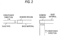
- the present invention provides a tape material for manufacturing an ignition plug electrode, the tape material being a member for forming an electrode chip, in which a base metal layer and a precious metal layer are cladded, on a bonded region set on an electrode base material of an ignition plug, the tape material being in the form of a long tape in which the base metal layer that is suitable for being in contact with the bonded region is cladded with the precious metal layer that is in contact with the base metal layer, the base metal layer having a width substantially equal to one of the longitudinal width, lateral width and diameter of the bonded region.
- electrode chips are individually produced, and individually bonded to a base material of a plug.
- the present invention uses a clad-shaped tape material in which chips having the same structure as that of the above-mentioned electrode chips are continuously connected.
- a tape material is conveyed to an electrode base material of a plug, and bonded to the electrode base material by resistance welding etc., and the tape material is cut to form electrode chips ( Fig. 1 ).
- the series of operations are more efficient than handling very small electrode chips one by one, and can contribute to reduction of equipment costs.
- the present invention provides a tape-shaped member in which a base metal layer to be bonded to a base material of a plug electrode and a precious metal layer that is in contact with the base metal layer are cladded.
- the precious metal layer includes a metal that is charged and discharged as an electrode of a plug, and the metal is preferably Pt or a Pt alloy, or Ir or an Ir alloy.
- the Pt alloy include Pt-Rh alloys, Pt-lr alloys, Pt-Ni alloys and Pt-Cu alloys.
- the Pt concentration here is preferably not less than 60% by mass and not more than 97% by mass.
- Specific examples of the Ir alloy include Ir-Rh alloys, Ir-Fe alloys, Ir-FeNi alloys and Ir-Cr alloys.
- the Ir concentration of the Ir alloy is preferably not less than 50% by mass and not more than 99% by mass.
- an alloy of Ir and Pt i.e. an Ir-Pt alloy (having a Pt concentration of not less than 3% by mass and not more than 40% by mass) can also be applied.
- the base metal layer is preferably one including Ni or a Ni alloy, or Cu or a Cu alloy.
- the Ni alloy or Cu alloy include Ni-Cr alloys, Ni-Fe-Al alloys, Ni-Fe-Co alloys, Ni-Pt alloys, Ni-Pd alloys, Ni-Ir alloys, Cu-Cr alloys, Cu-Ni alloys, Cu-W alloys, Cu-Pt alloys, Cu-Ir alloys and Cu-Pd alloys.
- a heat-resistance Ni-based alloy such as an inconel alloy can be suitably used.
- the width of the tape material may be such that the width of the base metal layer bonded to the base material of the electrode is substantially equal to that of the bonded region of the base material.
- the bonded region is a rectangular or circular region which is defined on a surface of the base material, and defines the bottom surface of an electrode chip formed on the base material.
- the longitudinal width, lateral width or diameter of the bonded region is smaller in size than each of the longitudinal width and the lateral width of the base material.
- the width of the base metal layer of the tape material is equal to the longitudinal width or the lateral width of the bonded region is determined by a conveyance direction of the tape material with respect to the base material (see Fig. 2 ).
- the width of the precious metal layer may be equal to that of the base metal layer, or may be smaller than that of the base metal layer.
- the thickness of each of the precious metal layer and the base metal layer is not particularly limited.
- the precious metal layer is an consumable part that is subject to loads of charge and discharge, and the thickness of the precious metal layer is appropriately determined with consideration given to the electrode life and electric characteristics.
- the thickness of the base metal layer is preferably not less than 1.5 times and not more than 5 times as large as the thickness of the precious metal layer.
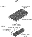
- the direction of the precious metal layer/base metal layer may be a longitudinal or lateral direction.
- a configuration (referred to as an overlay) is employed in which the precious metal layer and the base metal layer are laminated vertically (in a perpendicular direction).
- a plug with an earth electrode having a shape in which the precious metal part is protruded has been also developed, and for this application, a configuration (referred to as an edge-lay) may be employed in which the base metal layer and the precious metal layer are laminated laterally (in a horizontal direction) ( Fig. 3 ).
- an intermediate layer may be formed between the precious metal layer and the base metal layer.
- the intermediate layer includes an alloy of Ni and a precious metal or an alloy of Cu and a precious metal.
- the intermediate layer is a diffusion layer formed through a heat history in bonding of the precious metal layer and the base metal layer in the process for producing the tape material.
- the intermediate layer is an alloy metal layer having a gradient composition (precious metal concentration). Existence of the intermediate layer improves the bonding strength between the precious metal layer and the base metal layer.
- the thickness of the diffusion layer is preferably not less than 5 ⁇ m and not more than 150 ⁇ m.
- a tape material is supplied and bonded to an electrode base material of a plug, and cut to form an electrode chip on the electrode base material.
- bonding of the tape material to the electrode base material is preferably performed by resistance welding. Resistance welding allows an efficient bonding of the tape material to a very small region in a short time, and is suitable for formation of a plug electrode.
- At least one protrusion is formed on a surface of the base metal layer on the bonded region side in the cross-section shape.
- the projection(s) resistance heat generation can be concentrated to perform efficient welding in resistance welding.
- one projection, or a plurality of projections may be formed. Since the member according to the present invention is a tape-shaped member, the actual shape of the formed projection is in the form of a line.
- Production of the tape material for a plug electrode according to the present invention is essentially based on a process for producing a tape material having a usual clad structure. Specifically, a tape material for each of a precious metal layer and a base metal layer is processed, and both the tape materials are laid on each other, and rolled to produce a tape material having a clad structure. When a projection is formed on a surface of the base metal layer on the bonded region side, processing into a tape material and formation of the projection can be performed at the same time by using a roll with an appropriate pattern in production of a tape material for the base metal layer.
- a heat treatment is performed after the tape material for the precious metal layer and the tape material for the base metal layer are cladded.
- the heat treatment is performed for the purpose of improving the bonding strength by forming an intermediate layer (diffusion layer) at the interface between the precious metal layer and the base metal layer.
- the heat treatment is performed by heating at a temperature of not lower than 800°C and not higher than 1200°C in a non-oxidizing atmosphere (vacuum atmosphere, inert gas atmosphere or the like).
- the bonding strength between the precious metal layer and the base metal layer can be further improved.
- the plating is useful when a Ni alloy such as inconel, or a Cu alloy is used in the base metal layer.
- the thickness of the Ni plating or Cu plating is preferably not less than 0.5 ⁇ m and not more than 20 ⁇ m.
- the above-described tape material for a plug electrode according to the present invention is suitable for production of ignition plug electrode chips.
- the electrode chip is formed by cutting the tape material according to the present invention to an arbitrary length.
- An ignition plug including the electrode chip on a base material is excellent in production efficiency.
- the specific process of a method or producing an electrode chip and an ignition plug includes the step of supplying a tape material according to the present invention to an electrode base material of an ignition plug, positioning the tape material, then bonding a base metal layer of the tape material to the electrode base material by resistance welding etc., and then cutting the tape material.
- the tape material is bonded in the form of electrode chips. After the bonding, molding processing may be performed by use of a mold.
- electrode chips each including a precious metal layer and a base metal layer have been individually separated and isolated heretofore, and the present invention provides a member including these electrode chips in the form of a tape. According to the present invention, electrode chips can be efficiently produced by using a member having improved handling characteristics.
- a tape material was produced in which a precious metal layer including a Pt alloy and a base metal layer including a Ni alloy were cladded.
- a wire formed of a Pt alloy (Pt-20 wt% Ir) (line diameter: 1.0 mm, total length: 100 mm), and a wire formed of a Ni alloy (inconel 600) (line diameter: 1.0 mm, a total length: 100 mm) were provided, and were each drawing-processed to a diameter of 0.86 mm.
- the processed Pt alloy wire and Ni alloy wire were each rolling-processed into a 0.2 mm-thick tape material.
- a projection was formed by use of a roll with a groove on one surface side.
- the bonded surface of the Ni alloy was plated with Ni in a thickness of 1 ⁇ m.
- the Pt alloy tape and the Ni alloy tape were cladded by a roll.
- the tape material was fed into a nitrogen furnace, and heat-treated at 1000°C for 1 hour. Thereafter, finishing molding processing was performed to produce a tape material of clad structure having a trapezoidal cross-section.
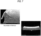
- Fig. 5 which is a photograph showing cross-section structures, shows that a favorable bonded part free from delamination and abnormal deformation at the interface between the precious metal layer and the base metal layer is obtained.
- the element distribution was analyzed by EPMA for the bonded interface, results as shown in Fig. 6 were obtained. It is apparent that at the bonded interface between the precious metal layer and the base metal layer, a diffusion layer including a precious metal (Pt, Ir) and components of a Ni alloy (Ni, Cr and Fe) exists as an intermediate layer.
- the diffusion layer had a thickness of about 20 ⁇ m.
- the bonding strength under a heat cycle load was evaluated for the produced clad tape.
- a sample obtained by cutting the tape material was put in an electric furnace, a cycle of operation including holding the sample at a heating temperature of 900°C for 360 seconds and at a cooling temperature of 70°C for 360 seconds was carried out 200 times, the sample was then taken out from the furnace, and its external appearance and bonded interface were observed.
- Results of the heat cycle test are shown in Fig. 7 .
- the tape material was oxidized at or near the end of the bonded interface as a result of receiving the heat cycle, but was not delaminated at the interface, and maintained a favorable state.
- the tape material When used with a plug electrode, the tape material may be in a favorable state with a reduced possibility of falling-off of the precious metal part.
- bonding between a precious metal chip and a substrate can be reliably maintained to prolong the life of an ignition plug, and therefore precious metals can be efficiently used to save resources.
Landscapes
- Engineering & Computer Science (AREA)
- Manufacturing & Machinery (AREA)
- Mechanical Engineering (AREA)
- Spark Plugs (AREA)
Claims (4)
- Bandmaterial zur Herstellung einer Zündkerzenelektrode, wobei das Bandmaterial zur Bildung von Elektrodenchips verwendet wird, in denen eine Grundmetallschicht und eine Edelmetallschicht auf einen Bondbereich, der auf einem Elektrodengrundmaterial einer Zündkerze aufgesetzt ist, aufgetragen sind, wobei die Elektrodenchips ununterbrochen verbunden sind, wobei das Bandmaterial in Form eines langen Bandes vorliegt, in dem die Grundmetallschicht, die geeignet ist, mit dem Bondbereich in Kontakt zu stehen, mit der Edelmetallschicht, die mit der Grundmetallschicht in Kontakt steht, aufgetragen ist, wobei die Grundmetallschicht des Bandmaterials eine Breite aufweist, die im Wesentlichen gleich zu einer der Längsbreite, Querbreite und dem Durchmesser des Bondbereichs ist,
dadurch gekennzeichnet, dass mindestens
ein Vorsprung auf einer Oberfläche der Grundmetallschicht auf der Seite des Bondbereichs in der Querschnittsform des Bandmaterials gebildet ist, wobei der Vorsprung in Form einer Linie vorliegt. - Bandmaterial zur Herstellung einer Zündkerzenelektrode nach Anspruch 1, wobei die Grundmetallschicht Ni oder eine Ni-Legierung oder Cu oder eine Cu-Legierung umfasst.
- Bandmaterial zur Herstellung einer Zündkerzenelektrode nach Anspruch 1 oder 2, wobei die Edelmetallschicht Pt oder eine Pt-Legierung oder Ir oder eine Ir-Legierung umfasst.
- Verfahren zur Herstellung einer Zündkerze, umfassend den Schritt Verbinden eines Elektrodenchips mit einem Elektrodengrundmaterial einer Zündkerze durch Verwendung des Bandmaterials zur Herstellung einer Zündkerze wie in einem der Ansprüche 1 bis 3 definiert, wobei das Verfahren den Schritt Zuführen des Bandmaterials zu dem Elektrodengrundmaterial der Zündkerze, Positionieren des Bandmaterials, Verbinden einer Grundmetallschicht des Bandmaterials mit dem Elektrodengrundmaterial durch Widerstandsschweißen, und dann Schneiden des Bandmaterials umfasst.
Applications Claiming Priority (2)
| Application Number | Priority Date | Filing Date | Title |
|---|---|---|---|
| JP2014191382A JP5948385B2 (ja) | 2014-09-19 | 2014-09-19 | 点火プラグ用電極を製造するためのクラッド構造を有するテープ材 |
| PCT/JP2015/075794 WO2016043130A1 (ja) | 2014-09-19 | 2015-09-11 | 点火プラグ用電極を製造するためのクラッド構造を有するテープ材 |
Publications (3)
| Publication Number | Publication Date |
|---|---|
| EP3196995A1 EP3196995A1 (de) | 2017-07-26 |
| EP3196995A4 EP3196995A4 (de) | 2018-04-25 |
| EP3196995B1 true EP3196995B1 (de) | 2020-03-18 |
Family
ID=55533168
Family Applications (1)
| Application Number | Title | Priority Date | Filing Date |
|---|---|---|---|
| EP15841466.4A Active EP3196995B1 (de) | 2014-09-19 | 2015-09-11 | Bandmaterial mit kaschierter struktur zur herstellung einer zündkerzenelektrode |
Country Status (6)
| Country | Link |
|---|---|
| US (1) | US9806500B2 (de) |
| EP (1) | EP3196995B1 (de) |
| JP (1) | JP5948385B2 (de) |
| KR (1) | KR101909402B1 (de) |
| CN (1) | CN107078469B (de) |
| WO (1) | WO2016043130A1 (de) |
Families Citing this family (9)
| Publication number | Priority date | Publication date | Assignee | Title |
|---|---|---|---|---|
| CA3133822A1 (en) | 2019-03-22 | 2020-10-01 | Dmc Global Inc. | Cladded article with clad layer having varying thickness |
| US11870222B2 (en) | 2021-05-04 | 2024-01-09 | Federal-Mogul Ignition Gmbh | Spark plug electrode and method of manufacturing the same |
| US11901705B2 (en) | 2021-07-22 | 2024-02-13 | Federal-Mogul Ignition Gmbh | Electrode tip assembly for a spark plug and method of manufacturing the same |
| US11621544B1 (en) | 2022-01-14 | 2023-04-04 | Federal-Mogul Ignition Gmbh | Spark plug electrode and method of manufacturing the same |
| DE102023107904A1 (de) | 2022-03-29 | 2023-10-05 | Federal-Mogul Ignition Gmbh | Zündkerze, zündkerzenelektrode und verfahren zur herstellung derselben |
| AT526189A1 (de) * | 2022-05-25 | 2023-12-15 | Swacrit Systems Gmbh | Verfahren zur Herstellung einer Elektrode für eine Zündvorrichtung |
| US11837852B1 (en) | 2022-07-27 | 2023-12-05 | Federal-Mogul Ignition Gmbh | Spark plug electrode with electrode tip directly thermally coupled to heat dissipating core and method of manufacturing the same |
| US12027826B2 (en) * | 2022-10-24 | 2024-07-02 | Federal-Mogul Ignition Llc | Spark plug |
| US12191637B1 (en) | 2024-06-14 | 2025-01-07 | Federal-Mogul Ignition Gmbh | Spark plug with cooling features and method of manufacturing the same |
Family Cites Families (13)
| Publication number | Priority date | Publication date | Assignee | Title |
|---|---|---|---|---|
| DE3100677A1 (de) * | 1980-02-11 | 1981-11-26 | Opprecht, Paul, 8962 Bergdietikon, Aargau | Buckel zum elektrischen widerstandsschweissen von aluminiumblechen und verfahren zu seiner herstellung |
| JPH04329286A (ja) * | 1991-04-30 | 1992-11-18 | Nippondenso Co Ltd | スパークプラグの製造方法 |
| JP3196352B2 (ja) * | 1992-09-01 | 2001-08-06 | 株式会社デンソー | 内燃機関用スパークプラグの製造方法 |
| US20040092193A1 (en) * | 2001-02-13 | 2004-05-13 | Mamoru Musasa | Method of manufacturing spark plug |
| JP2002343533A (ja) * | 2001-03-15 | 2002-11-29 | Denso Corp | 内燃機関用スパークプラグ |
| JP4402871B2 (ja) | 2002-10-10 | 2010-01-20 | 日本特殊陶業株式会社 | スパークプラグの製造方法 |
| US7164225B2 (en) * | 2003-09-11 | 2007-01-16 | Ngk Spark Plug Co., Ltd. | Small size spark plug having side spark prevention |
| JP4603005B2 (ja) * | 2007-03-28 | 2010-12-22 | 日本特殊陶業株式会社 | スパークプラグの製造方法 |
| US8294343B2 (en) * | 2008-12-31 | 2012-10-23 | Fram Group Ip Llc | Method of producing a spark plug via flared tip attachment |
| JP2009302066A (ja) * | 2009-09-24 | 2009-12-24 | Ngk Spark Plug Co Ltd | スパークプラグの製造方法 |
| WO2013015262A1 (ja) * | 2011-07-28 | 2013-01-31 | 田中貴金属工業株式会社 | 点火プラグ用クラッド電極及びその製造方法 |
| CN103094842A (zh) * | 2013-01-18 | 2013-05-08 | 株洲湘火炬火花塞有限责任公司 | 一种火花塞复合电极头制作方法及复合电极头带 |
| US9368943B2 (en) * | 2013-03-12 | 2016-06-14 | Federal-Mogul Ignition Company | Spark plug having multi-layer sparking component attached to ground electrode |
-
2014
- 2014-09-19 JP JP2014191382A patent/JP5948385B2/ja active Active
-
2015
- 2015-09-11 WO PCT/JP2015/075794 patent/WO2016043130A1/ja not_active Ceased
- 2015-09-11 KR KR1020177010225A patent/KR101909402B1/ko active Active
- 2015-09-11 EP EP15841466.4A patent/EP3196995B1/de active Active
- 2015-09-11 CN CN201580049738.XA patent/CN107078469B/zh active Active
- 2015-09-11 US US15/504,500 patent/US9806500B2/en active Active
Non-Patent Citations (1)
| Title |
|---|
| None * |
Also Published As
| Publication number | Publication date |
|---|---|
| US20170264082A1 (en) | 2017-09-14 |
| US9806500B2 (en) | 2017-10-31 |
| EP3196995A1 (de) | 2017-07-26 |
| JP2016062825A (ja) | 2016-04-25 |
| KR101909402B1 (ko) | 2018-10-17 |
| JP5948385B2 (ja) | 2016-07-06 |
| KR20170054510A (ko) | 2017-05-17 |
| CN107078469B (zh) | 2020-07-24 |
| CN107078469A (zh) | 2017-08-18 |
| WO2016043130A1 (ja) | 2016-03-24 |
| EP3196995A4 (de) | 2018-04-25 |
Similar Documents
| Publication | Publication Date | Title |
|---|---|---|
| EP3196995B1 (de) | Bandmaterial mit kaschierter struktur zur herstellung einer zündkerzenelektrode | |
| KR101562151B1 (ko) | 점화 플러그용 클래드 전극 및 그 제조 방법 | |
| US6306523B1 (en) | Method of manufacturing porous electrode wire for electric discharge machining and structure of the electrode wire | |
| JP5221231B2 (ja) | 太陽電池用リード線の製造方法 | |
| JP4430119B2 (ja) | スパークプラグ用の貴金属合金及びその製造加工方法 | |
| KR102493928B1 (ko) | 냉간 금속 이행 공정에 의해 제조되는 점화 장치 구성요소 | |
| JP2010205792A (ja) | 太陽電池用リード線およびその製造方法並びにそれを用いた太陽電池 | |
| JP5161734B2 (ja) | 太陽電池用リード線及びその製造方法並びに太陽電池 | |
| KR100921704B1 (ko) | 판상형 복합 전기접점소자의 제조방법 | |
| TWI446372B (zh) | Metal plate low resistance chip resistor and manufacturing method thereof | |
| JP6298247B2 (ja) | 抵抗溶接用電極 | |
| TW202228168A (zh) | 加熱嘴及加熱嘴單元 | |
| KR100758013B1 (ko) | 전기접점 및 그 제조방법 | |
| JP6344605B2 (ja) | 半導体装置の製造方法 | |
| CN118299202A (zh) | 一种通过双面原位还原制备AgCuO/AgCu片状电触头的方法 | |
| CN119480475A (zh) | 一种层状复合电接触材料及其制备方法 | |
| JP2014007223A (ja) | 接続材料の供給方法及びそれを用いた半導体装置の製造方法 | |
| JP2019202322A (ja) | 複合金属材の製造方法 |
Legal Events
| Date | Code | Title | Description |
|---|---|---|---|
| STAA | Information on the status of an ep patent application or granted ep patent |
Free format text: STATUS: THE INTERNATIONAL PUBLICATION HAS BEEN MADE |
|
| PUAI | Public reference made under article 153(3) epc to a published international application that has entered the european phase |
Free format text: ORIGINAL CODE: 0009012 |
|
| STAA | Information on the status of an ep patent application or granted ep patent |
Free format text: STATUS: REQUEST FOR EXAMINATION WAS MADE |
|
| 17P | Request for examination filed |
Effective date: 20170222 |
|
| AK | Designated contracting states |
Kind code of ref document: A1 Designated state(s): AL AT BE BG CH CY CZ DE DK EE ES FI FR GB GR HR HU IE IS IT LI LT LU LV MC MK MT NL NO PL PT RO RS SE SI SK SM TR |
|
| AX | Request for extension of the european patent |
Extension state: BA ME |
|
| DAV | Request for validation of the european patent (deleted) | ||
| DAX | Request for extension of the european patent (deleted) | ||
| A4 | Supplementary search report drawn up and despatched |
Effective date: 20180328 |
|
| RIC1 | Information provided on ipc code assigned before grant |
Ipc: H01T 13/39 20060101AFI20180322BHEP Ipc: H01T 21/02 20060101ALI20180322BHEP |
|
| REG | Reference to a national code |
Ref country code: DE Ref legal event code: R079 Ref document number: 602015049137 Country of ref document: DE Free format text: PREVIOUS MAIN CLASS: H01T0013200000 Ipc: H01T0013390000 |
|
| RIC1 | Information provided on ipc code assigned before grant |
Ipc: H01T 21/02 20060101ALI20190821BHEP Ipc: H01T 13/39 20060101AFI20190821BHEP |
|
| GRAP | Despatch of communication of intention to grant a patent |
Free format text: ORIGINAL CODE: EPIDOSNIGR1 |
|
| STAA | Information on the status of an ep patent application or granted ep patent |
Free format text: STATUS: GRANT OF PATENT IS INTENDED |
|
| INTG | Intention to grant announced |
Effective date: 20191011 |
|
| GRAS | Grant fee paid |
Free format text: ORIGINAL CODE: EPIDOSNIGR3 |
|
| GRAA | (expected) grant |
Free format text: ORIGINAL CODE: 0009210 |
|
| STAA | Information on the status of an ep patent application or granted ep patent |
Free format text: STATUS: THE PATENT HAS BEEN GRANTED |
|
| AK | Designated contracting states |
Kind code of ref document: B1 Designated state(s): AL AT BE BG CH CY CZ DE DK EE ES FI FR GB GR HR HU IE IS IT LI LT LU LV MC MK MT NL NO PL PT RO RS SE SI SK SM TR |
|
| REG | Reference to a national code |
Ref country code: GB Ref legal event code: FG4D |
|
| REG | Reference to a national code |
Ref country code: DE Ref legal event code: R096 Ref document number: 602015049137 Country of ref document: DE |
|
| REG | Reference to a national code |
Ref country code: AT Ref legal event code: REF Ref document number: 1247033 Country of ref document: AT Kind code of ref document: T Effective date: 20200415 Ref country code: IE Ref legal event code: FG4D |
|
| PG25 | Lapsed in a contracting state [announced via postgrant information from national office to epo] |
Ref country code: NO Free format text: LAPSE BECAUSE OF FAILURE TO SUBMIT A TRANSLATION OF THE DESCRIPTION OR TO PAY THE FEE WITHIN THE PRESCRIBED TIME-LIMIT Effective date: 20200618 Ref country code: FI Free format text: LAPSE BECAUSE OF FAILURE TO SUBMIT A TRANSLATION OF THE DESCRIPTION OR TO PAY THE FEE WITHIN THE PRESCRIBED TIME-LIMIT Effective date: 20200318 Ref country code: RS Free format text: LAPSE BECAUSE OF FAILURE TO SUBMIT A TRANSLATION OF THE DESCRIPTION OR TO PAY THE FEE WITHIN THE PRESCRIBED TIME-LIMIT Effective date: 20200318 |
|
| REG | Reference to a national code |
Ref country code: NL Ref legal event code: MP Effective date: 20200318 |
|
| PG25 | Lapsed in a contracting state [announced via postgrant information from national office to epo] |
Ref country code: GR Free format text: LAPSE BECAUSE OF FAILURE TO SUBMIT A TRANSLATION OF THE DESCRIPTION OR TO PAY THE FEE WITHIN THE PRESCRIBED TIME-LIMIT Effective date: 20200619 Ref country code: HR Free format text: LAPSE BECAUSE OF FAILURE TO SUBMIT A TRANSLATION OF THE DESCRIPTION OR TO PAY THE FEE WITHIN THE PRESCRIBED TIME-LIMIT Effective date: 20200318 Ref country code: BG Free format text: LAPSE BECAUSE OF FAILURE TO SUBMIT A TRANSLATION OF THE DESCRIPTION OR TO PAY THE FEE WITHIN THE PRESCRIBED TIME-LIMIT Effective date: 20200618 Ref country code: SE Free format text: LAPSE BECAUSE OF FAILURE TO SUBMIT A TRANSLATION OF THE DESCRIPTION OR TO PAY THE FEE WITHIN THE PRESCRIBED TIME-LIMIT Effective date: 20200318 Ref country code: LV Free format text: LAPSE BECAUSE OF FAILURE TO SUBMIT A TRANSLATION OF THE DESCRIPTION OR TO PAY THE FEE WITHIN THE PRESCRIBED TIME-LIMIT Effective date: 20200318 |
|
| REG | Reference to a national code |
Ref country code: LT Ref legal event code: MG4D |
|
| PG25 | Lapsed in a contracting state [announced via postgrant information from national office to epo] |
Ref country code: NL Free format text: LAPSE BECAUSE OF FAILURE TO SUBMIT A TRANSLATION OF THE DESCRIPTION OR TO PAY THE FEE WITHIN THE PRESCRIBED TIME-LIMIT Effective date: 20200318 |
|
| PG25 | Lapsed in a contracting state [announced via postgrant information from national office to epo] |
Ref country code: EE Free format text: LAPSE BECAUSE OF FAILURE TO SUBMIT A TRANSLATION OF THE DESCRIPTION OR TO PAY THE FEE WITHIN THE PRESCRIBED TIME-LIMIT Effective date: 20200318 Ref country code: LT Free format text: LAPSE BECAUSE OF FAILURE TO SUBMIT A TRANSLATION OF THE DESCRIPTION OR TO PAY THE FEE WITHIN THE PRESCRIBED TIME-LIMIT Effective date: 20200318 Ref country code: PT Free format text: LAPSE BECAUSE OF FAILURE TO SUBMIT A TRANSLATION OF THE DESCRIPTION OR TO PAY THE FEE WITHIN THE PRESCRIBED TIME-LIMIT Effective date: 20200812 Ref country code: SM Free format text: LAPSE BECAUSE OF FAILURE TO SUBMIT A TRANSLATION OF THE DESCRIPTION OR TO PAY THE FEE WITHIN THE PRESCRIBED TIME-LIMIT Effective date: 20200318 Ref country code: CZ Free format text: LAPSE BECAUSE OF FAILURE TO SUBMIT A TRANSLATION OF THE DESCRIPTION OR TO PAY THE FEE WITHIN THE PRESCRIBED TIME-LIMIT Effective date: 20200318 Ref country code: IS Free format text: LAPSE BECAUSE OF FAILURE TO SUBMIT A TRANSLATION OF THE DESCRIPTION OR TO PAY THE FEE WITHIN THE PRESCRIBED TIME-LIMIT Effective date: 20200718 Ref country code: RO Free format text: LAPSE BECAUSE OF FAILURE TO SUBMIT A TRANSLATION OF THE DESCRIPTION OR TO PAY THE FEE WITHIN THE PRESCRIBED TIME-LIMIT Effective date: 20200318 Ref country code: SK Free format text: LAPSE BECAUSE OF FAILURE TO SUBMIT A TRANSLATION OF THE DESCRIPTION OR TO PAY THE FEE WITHIN THE PRESCRIBED TIME-LIMIT Effective date: 20200318 |
|
| REG | Reference to a national code |
Ref country code: AT Ref legal event code: MK05 Ref document number: 1247033 Country of ref document: AT Kind code of ref document: T Effective date: 20200318 |
|
| REG | Reference to a national code |
Ref country code: DE Ref legal event code: R097 Ref document number: 602015049137 Country of ref document: DE |
|
| PLBE | No opposition filed within time limit |
Free format text: ORIGINAL CODE: 0009261 |
|
| STAA | Information on the status of an ep patent application or granted ep patent |
Free format text: STATUS: NO OPPOSITION FILED WITHIN TIME LIMIT |
|
| PG25 | Lapsed in a contracting state [announced via postgrant information from national office to epo] |
Ref country code: ES Free format text: LAPSE BECAUSE OF FAILURE TO SUBMIT A TRANSLATION OF THE DESCRIPTION OR TO PAY THE FEE WITHIN THE PRESCRIBED TIME-LIMIT Effective date: 20200318 Ref country code: DK Free format text: LAPSE BECAUSE OF FAILURE TO SUBMIT A TRANSLATION OF THE DESCRIPTION OR TO PAY THE FEE WITHIN THE PRESCRIBED TIME-LIMIT Effective date: 20200318 Ref country code: AT Free format text: LAPSE BECAUSE OF FAILURE TO SUBMIT A TRANSLATION OF THE DESCRIPTION OR TO PAY THE FEE WITHIN THE PRESCRIBED TIME-LIMIT Effective date: 20200318 |
|
| 26N | No opposition filed |
Effective date: 20201221 |
|
| PG25 | Lapsed in a contracting state [announced via postgrant information from national office to epo] |
Ref country code: PL Free format text: LAPSE BECAUSE OF FAILURE TO SUBMIT A TRANSLATION OF THE DESCRIPTION OR TO PAY THE FEE WITHIN THE PRESCRIBED TIME-LIMIT Effective date: 20200318 |
|
| PG25 | Lapsed in a contracting state [announced via postgrant information from national office to epo] |
Ref country code: MC Free format text: LAPSE BECAUSE OF FAILURE TO SUBMIT A TRANSLATION OF THE DESCRIPTION OR TO PAY THE FEE WITHIN THE PRESCRIBED TIME-LIMIT Effective date: 20200318 |
|
| REG | Reference to a national code |
Ref country code: CH Ref legal event code: PL |
|
| GBPC | Gb: european patent ceased through non-payment of renewal fee |
Effective date: 20200911 |
|
| PG25 | Lapsed in a contracting state [announced via postgrant information from national office to epo] |
Ref country code: SI Free format text: LAPSE BECAUSE OF FAILURE TO SUBMIT A TRANSLATION OF THE DESCRIPTION OR TO PAY THE FEE WITHIN THE PRESCRIBED TIME-LIMIT Effective date: 20200318 |
|
| REG | Reference to a national code |
Ref country code: BE Ref legal event code: MM Effective date: 20200930 |
|
| PG25 | Lapsed in a contracting state [announced via postgrant information from national office to epo] |
Ref country code: LU Free format text: LAPSE BECAUSE OF NON-PAYMENT OF DUE FEES Effective date: 20200911 |
|
| PG25 | Lapsed in a contracting state [announced via postgrant information from national office to epo] |
Ref country code: LI Free format text: LAPSE BECAUSE OF NON-PAYMENT OF DUE FEES Effective date: 20200930 Ref country code: GB Free format text: LAPSE BECAUSE OF NON-PAYMENT OF DUE FEES Effective date: 20200911 Ref country code: IE Free format text: LAPSE BECAUSE OF NON-PAYMENT OF DUE FEES Effective date: 20200911 Ref country code: CH Free format text: LAPSE BECAUSE OF NON-PAYMENT OF DUE FEES Effective date: 20200930 Ref country code: BE Free format text: LAPSE BECAUSE OF NON-PAYMENT OF DUE FEES Effective date: 20200930 |
|
| PG25 | Lapsed in a contracting state [announced via postgrant information from national office to epo] |
Ref country code: TR Free format text: LAPSE BECAUSE OF FAILURE TO SUBMIT A TRANSLATION OF THE DESCRIPTION OR TO PAY THE FEE WITHIN THE PRESCRIBED TIME-LIMIT Effective date: 20200318 Ref country code: MT Free format text: LAPSE BECAUSE OF FAILURE TO SUBMIT A TRANSLATION OF THE DESCRIPTION OR TO PAY THE FEE WITHIN THE PRESCRIBED TIME-LIMIT Effective date: 20200318 Ref country code: CY Free format text: LAPSE BECAUSE OF FAILURE TO SUBMIT A TRANSLATION OF THE DESCRIPTION OR TO PAY THE FEE WITHIN THE PRESCRIBED TIME-LIMIT Effective date: 20200318 |
|
| PG25 | Lapsed in a contracting state [announced via postgrant information from national office to epo] |
Ref country code: MK Free format text: LAPSE BECAUSE OF FAILURE TO SUBMIT A TRANSLATION OF THE DESCRIPTION OR TO PAY THE FEE WITHIN THE PRESCRIBED TIME-LIMIT Effective date: 20200318 Ref country code: AL Free format text: LAPSE BECAUSE OF FAILURE TO SUBMIT A TRANSLATION OF THE DESCRIPTION OR TO PAY THE FEE WITHIN THE PRESCRIBED TIME-LIMIT Effective date: 20200318 |
|
| PGFP | Annual fee paid to national office [announced via postgrant information from national office to epo] |
Ref country code: DE Payment date: 20250919 Year of fee payment: 11 |
|
| PGFP | Annual fee paid to national office [announced via postgrant information from national office to epo] |
Ref country code: IT Payment date: 20250923 Year of fee payment: 11 |
|
| PGFP | Annual fee paid to national office [announced via postgrant information from national office to epo] |
Ref country code: FR Payment date: 20250922 Year of fee payment: 11 |