EP3195428B1 - Dispositif laser a cavite externe verticale a emission par la surface a double frequences, pour la generation de thz et procede de generation de thz. - Google Patents
Dispositif laser a cavite externe verticale a emission par la surface a double frequences, pour la generation de thz et procede de generation de thz. Download PDFInfo
- Publication number
- EP3195428B1 EP3195428B1 EP15775115.7A EP15775115A EP3195428B1 EP 3195428 B1 EP3195428 B1 EP 3195428B1 EP 15775115 A EP15775115 A EP 15775115A EP 3195428 B1 EP3195428 B1 EP 3195428B1
- Authority
- EP
- European Patent Office
- Prior art keywords
- transverse
- optical wave
- modes
- optical
- laser
- Prior art date
- Legal status (The legal status is an assumption and is not a legal conclusion. Google has not performed a legal analysis and makes no representation as to the accuracy of the status listed.)
- Active
Links
Images


Classifications
-
- H—ELECTRICITY
- H01—ELECTRIC ELEMENTS
- H01S—DEVICES USING THE PROCESS OF LIGHT AMPLIFICATION BY STIMULATED EMISSION OF RADIATION [LASER] TO AMPLIFY OR GENERATE LIGHT; DEVICES USING STIMULATED EMISSION OF ELECTROMAGNETIC RADIATION IN WAVE RANGES OTHER THAN OPTICAL
- H01S5/00—Semiconductor lasers
- H01S5/10—Construction or shape of the optical resonator, e.g. extended or external cavity, coupled cavities, bent-guide, varying width, thickness or composition of the active region
- H01S5/14—External cavity lasers
-
- H—ELECTRICITY
- H01—ELECTRIC ELEMENTS
- H01S—DEVICES USING THE PROCESS OF LIGHT AMPLIFICATION BY STIMULATED EMISSION OF RADIATION [LASER] TO AMPLIFY OR GENERATE LIGHT; DEVICES USING STIMULATED EMISSION OF ELECTROMAGNETIC RADIATION IN WAVE RANGES OTHER THAN OPTICAL
- H01S3/00—Lasers, i.e. devices using stimulated emission of electromagnetic radiation in the infrared, visible or ultraviolet wave range
- H01S3/05—Construction or shape of optical resonators; Accommodation of active medium therein; Shape of active medium
- H01S3/08—Construction or shape of optical resonators or components thereof
- H01S3/08018—Mode suppression
- H01S3/0804—Transverse or lateral modes
-
- H—ELECTRICITY
- H01—ELECTRIC ELEMENTS
- H01S—DEVICES USING THE PROCESS OF LIGHT AMPLIFICATION BY STIMULATED EMISSION OF RADIATION [LASER] TO AMPLIFY OR GENERATE LIGHT; DEVICES USING STIMULATED EMISSION OF ELECTROMAGNETIC RADIATION IN WAVE RANGES OTHER THAN OPTICAL
- H01S3/00—Lasers, i.e. devices using stimulated emission of electromagnetic radiation in the infrared, visible or ultraviolet wave range
- H01S3/10—Controlling the intensity, frequency, phase, polarisation or direction of the emitted radiation, e.g. switching, gating, modulating or demodulating
- H01S3/106—Controlling the intensity, frequency, phase, polarisation or direction of the emitted radiation, e.g. switching, gating, modulating or demodulating by controlling devices placed within the cavity
- H01S3/1065—Controlling the intensity, frequency, phase, polarisation or direction of the emitted radiation, e.g. switching, gating, modulating or demodulating by controlling devices placed within the cavity using liquid crystals
-
- H—ELECTRICITY
- H01—ELECTRIC ELEMENTS
- H01S—DEVICES USING THE PROCESS OF LIGHT AMPLIFICATION BY STIMULATED EMISSION OF RADIATION [LASER] TO AMPLIFY OR GENERATE LIGHT; DEVICES USING STIMULATED EMISSION OF ELECTROMAGNETIC RADIATION IN WAVE RANGES OTHER THAN OPTICAL
- H01S5/00—Semiconductor lasers
- H01S5/005—Optical components external to the laser cavity, specially adapted therefor, e.g. for homogenisation or merging of the beams or for manipulating laser pulses, e.g. pulse shaping
- H01S5/0078—Optical components external to the laser cavity, specially adapted therefor, e.g. for homogenisation or merging of the beams or for manipulating laser pulses, e.g. pulse shaping for frequency filtering
-
- H—ELECTRICITY
- H01—ELECTRIC ELEMENTS
- H01S—DEVICES USING THE PROCESS OF LIGHT AMPLIFICATION BY STIMULATED EMISSION OF RADIATION [LASER] TO AMPLIFY OR GENERATE LIGHT; DEVICES USING STIMULATED EMISSION OF ELECTROMAGNETIC RADIATION IN WAVE RANGES OTHER THAN OPTICAL
- H01S5/00—Semiconductor lasers
- H01S5/10—Construction or shape of the optical resonator, e.g. extended or external cavity, coupled cavities, bent-guide, varying width, thickness or composition of the active region
- H01S5/1092—Multi-wavelength lasing
- H01S5/1096—Multi-wavelength lasing in a single cavity
-
- H—ELECTRICITY
- H01—ELECTRIC ELEMENTS
- H01S—DEVICES USING THE PROCESS OF LIGHT AMPLIFICATION BY STIMULATED EMISSION OF RADIATION [LASER] TO AMPLIFY OR GENERATE LIGHT; DEVICES USING STIMULATED EMISSION OF ELECTROMAGNETIC RADIATION IN WAVE RANGES OTHER THAN OPTICAL
- H01S5/00—Semiconductor lasers
- H01S5/10—Construction or shape of the optical resonator, e.g. extended or external cavity, coupled cavities, bent-guide, varying width, thickness or composition of the active region
- H01S5/11—Comprising a photonic bandgap structure
-
- H—ELECTRICITY
- H01—ELECTRIC ELEMENTS
- H01S—DEVICES USING THE PROCESS OF LIGHT AMPLIFICATION BY STIMULATED EMISSION OF RADIATION [LASER] TO AMPLIFY OR GENERATE LIGHT; DEVICES USING STIMULATED EMISSION OF ELECTROMAGNETIC RADIATION IN WAVE RANGES OTHER THAN OPTICAL
- H01S5/00—Semiconductor lasers
- H01S5/10—Construction or shape of the optical resonator, e.g. extended or external cavity, coupled cavities, bent-guide, varying width, thickness or composition of the active region
- H01S5/18—Surface-emitting [SE] lasers, e.g. having both horizontal and vertical cavities
- H01S5/183—Surface-emitting [SE] lasers, e.g. having both horizontal and vertical cavities having only vertical cavities, e.g. vertical cavity surface-emitting lasers [VCSEL]
- H01S5/18361—Structure of the reflectors, e.g. hybrid mirrors
-
- H—ELECTRICITY
- H01—ELECTRIC ELEMENTS
- H01S—DEVICES USING THE PROCESS OF LIGHT AMPLIFICATION BY STIMULATED EMISSION OF RADIATION [LASER] TO AMPLIFY OR GENERATE LIGHT; DEVICES USING STIMULATED EMISSION OF ELECTROMAGNETIC RADIATION IN WAVE RANGES OTHER THAN OPTICAL
- H01S2301/00—Functional characteristics
- H01S2301/16—Semiconductor lasers with special structural design to influence the modes, e.g. specific multimode
-
- H—ELECTRICITY
- H01—ELECTRIC ELEMENTS
- H01S—DEVICES USING THE PROCESS OF LIGHT AMPLIFICATION BY STIMULATED EMISSION OF RADIATION [LASER] TO AMPLIFY OR GENERATE LIGHT; DEVICES USING STIMULATED EMISSION OF ELECTROMAGNETIC RADIATION IN WAVE RANGES OTHER THAN OPTICAL
- H01S2302/00—Amplification / lasing wavelength
- H01S2302/02—THz - lasers, i.e. lasers with emission in the wavelength range of typically 0.1 mm to 1 mm
-
- H—ELECTRICITY
- H01—ELECTRIC ELEMENTS
- H01S—DEVICES USING THE PROCESS OF LIGHT AMPLIFICATION BY STIMULATED EMISSION OF RADIATION [LASER] TO AMPLIFY OR GENERATE LIGHT; DEVICES USING STIMULATED EMISSION OF ELECTROMAGNETIC RADIATION IN WAVE RANGES OTHER THAN OPTICAL
- H01S5/00—Semiconductor lasers
- H01S5/04—Processes or apparatus for excitation, e.g. pumping, e.g. by electron beams
- H01S5/041—Optical pumping
-
- H—ELECTRICITY
- H01—ELECTRIC ELEMENTS
- H01S—DEVICES USING THE PROCESS OF LIGHT AMPLIFICATION BY STIMULATED EMISSION OF RADIATION [LASER] TO AMPLIFY OR GENERATE LIGHT; DEVICES USING STIMULATED EMISSION OF ELECTROMAGNETIC RADIATION IN WAVE RANGES OTHER THAN OPTICAL
- H01S5/00—Semiconductor lasers
- H01S5/10—Construction or shape of the optical resonator, e.g. extended or external cavity, coupled cavities, bent-guide, varying width, thickness or composition of the active region
- H01S5/18—Surface-emitting [SE] lasers, e.g. having both horizontal and vertical cavities
- H01S5/183—Surface-emitting [SE] lasers, e.g. having both horizontal and vertical cavities having only vertical cavities, e.g. vertical cavity surface-emitting lasers [VCSEL]
- H01S5/18308—Surface-emitting [SE] lasers, e.g. having both horizontal and vertical cavities having only vertical cavities, e.g. vertical cavity surface-emitting lasers [VCSEL] having a special structure for lateral current or light confinement
- H01S5/18319—Surface-emitting [SE] lasers, e.g. having both horizontal and vertical cavities having only vertical cavities, e.g. vertical cavity surface-emitting lasers [VCSEL] having a special structure for lateral current or light confinement comprising a periodical structure in lateral directions
-
- H—ELECTRICITY
- H01—ELECTRIC ELEMENTS
- H01S—DEVICES USING THE PROCESS OF LIGHT AMPLIFICATION BY STIMULATED EMISSION OF RADIATION [LASER] TO AMPLIFY OR GENERATE LIGHT; DEVICES USING STIMULATED EMISSION OF ELECTROMAGNETIC RADIATION IN WAVE RANGES OTHER THAN OPTICAL
- H01S5/00—Semiconductor lasers
- H01S5/10—Construction or shape of the optical resonator, e.g. extended or external cavity, coupled cavities, bent-guide, varying width, thickness or composition of the active region
- H01S5/18—Surface-emitting [SE] lasers, e.g. having both horizontal and vertical cavities
- H01S5/183—Surface-emitting [SE] lasers, e.g. having both horizontal and vertical cavities having only vertical cavities, e.g. vertical cavity surface-emitting lasers [VCSEL]
- H01S5/18361—Structure of the reflectors, e.g. hybrid mirrors
- H01S5/18369—Structure of the reflectors, e.g. hybrid mirrors based on dielectric materials
Definitions
- the present invention relates to vertical external cavity surface emitting laser devices (VeCSEL for "Vertical External Cavity Surface Emitting Laser”), and more specifically the generation of two stabilized transverse modes with such devices.
- VeCSEL Vertical External Cavity Surface Emitting Laser
- the field of the invention is, without limitation, that of semiconductor laser terahertz (THz) sources as well as their applications.
- THz waves cover the electromagnetic spectrum between microwaves and infrared.
- the field of application is very broad with some promising applications, such as for example in astronomy, in radar systems, in time-frequency metrology, in biomedical detection and imaging, in high-speed wireless communications or in Security.
- bandwidth in the upper range of the THz spectrum, the sources are generally of the pulsed type and / or require operation at low temperature; and in the lower range of the THz spectrum, electronic sources usually operate easily at room temperature continuously and at a determined transmission frequency.
- multiple frequency sources offer increased tunability but do not simultaneously provide both sufficient output power and large bandwidth modulation, but also good compactness or reasonable cost.
- Another technique is an external cavity laser diode using a spectral (spectral) filter (s) which can produce two stable frequencies, but at the expense of output power, complex cavities, sensitivity / robustness. Degraded alignment, beam quality and coherence because the laser tends to exploit two sets of longitudinal modes rather than two modes.
- spectral filter s
- VeCSEL Surface Emitting Vertical External Cavity Laser
- VeCSEL is described in Gaya Baili et al., “Experimental demonstration of a tunable dual-frequency semiconductor laser free of relaxation oscillations”, Optics Letters, Vol. 34, Issue 21, pages 3421-3423 (2009 ). It deals with the use of a VeCSEL in the GHz range and is based on a dual polarization beam with intracavity beam splitting on the amplifier chip.
- the aim of the present invention is to respond to the problems mentioned above and also to lead to other advantages.
- An objective of the invention consists in generating a laser effect with two transverse modes, stable and robust / controlled within a single cavity.
- Another object of the present invention is to provide laser sources exhibiting a very high stability (that is to say a high coherence or a low phase noise) of the beat frequency.
- Another objective of the present invention is to provide laser sources suitable for high power operations with good consistency and good stability.
- Another objective of the invention consists in providing laser sources having continuous or fine tunability over a wide range of frequencies.
- Another objective of the invention consists in providing compact laser sources operating at ambient temperature in continuous mode.
- the light intensity shaping means comprise at least one mask, each mask being arranged with a surface having non-uniform absorbance, said surface including at least one absorption zone and / or at least a transmission area;
- the means for shaping the phase profile of the optical wave are arranged to adjust the at least two transverse modes of the optical wave, and in particular comprise at least one photonic crystal and / or a diffraction grating located at least one end of the gain region and arranged to shape the transverse phase and / or the transverse intensity of the optical wave, to select at least two transverse modes.
- the (any) gain region may be a separate element from the second mirror.
- the number of stabilized frequencies emitted by the laser according to the invention corresponds to the number of transverse modes selected.
- the means for pumping the gain region may include optical and electrical means.
- the first element can be a semiconductor element of half-VCSEL type, or any other type of laser in which the transverse modes can resonate inside the cavity.
- the laser device according to the present invention takes advantage of the VeCSEL structures in terms of output power, stability and robustness.
- the use of half a VCSEL allows the laser device according to the present invention to be used at room temperature and in a continuous mode, which greatly simplifies its use and makes it more versatile.
- the intrinsic optical qualities of the cavity are very good and are particularly suitable for such applications: the optical losses are low and there is no amplified spontaneous emission, which leads to a highly coherent wave.
- the at least two selected transverse modes of the optical wave according to the present invention can be chosen between (i) the stabilized Laguerre-Gauss modes, and / or (ii) the stabilized Hermite-Gauss modes and / or (iii) stabilized Bessel-Gauss modes or any other laser emission state: other transverse mode bases of the cavity (eigenstates of light) - or unstable modes of the cavity - can be used, provided they are generated simultaneously.
- the means for spatial filtering of the optical wave can be chosen from (i) means for diffraction of light, (ii) means for scattering light and (iii) means for absorption light.
- the means for spatial filtering of the optical wave can be located at a belly of the stationary longitudinal field inside the cavity.
- the light absorption means can comprise a single mask, said mask being arranged to select the at least two transverse modes of the optical wave.
- the means for absorption or diffraction of light mentioned above can be integrated on the semiconductor element.
- the present invention makes it possible to stabilize resonant modes inside the cavity by selecting these isolated transverse modes and by preventing coupling with certain undesired modes: the laser source according to the invention provides a very stable beat frequency.
- the thickness of each mask may be of the order of a few nanometers or less than the wavelength.
- the absorption zone provides an absorbance at least twice as high as the absorbance of the transmission zone.
- the transmitting areas can transmit more than 99% of the light intensity of the wave, and the absorption areas can absorb between 5% and 100% of the light intensity of the wave. .
- each mask can be located at the level of a belly of the optical wave inside the cavity, or close to said belly.
- the means for shaping the longitudinal phase profile has a non-uniform transverse distribution of the gain inside the optical cavity, in order to transversely modulate the intensity of the emission wavelength of the gain and to adjust the frequency difference between the at least two transverse modes of the optical wave.
- the means for shaping the longitudinal phase profile may further comprise at least one loss mask which is not uniform transversely between the two modes in order to adjust the frequency difference between the two modes by locally adjusting the carriers injected into the gain zones to modify the emission length of the gain on these zones.
- the fine adjustment of the oscillating transverse modes inside the cavity can be obtained using a means for shaping the phase profile comprising a heat source arranged to generate inside the cavity optically a non-uniform transverse distribution of temperature, in order to determine and control the frequency difference between the at least two transverse modes of the optical wave.
- the means for shaping the phase profile comprises a spectral filter having a non-uniform optical length along its transverse section in order to adjust the frequency difference between the two transverse modes of said wave optical.
- the means for shaping the phase profile can be arranged to modify the index of refraction “seen” by the optical wave and by at least one of the transverse modes oscillating inside. the cavity.
- the refractive index is, in the first order, sensitive to the temperature, to the pressure and to the hygrometry of the medium through which the optical wave passes
- such a means for shaping the phase profile can consist of a means which varies the pressure and / or the hygrometry and / or the temperature of at least part of the path taken by the optical wave inside the cavity.
- the means for shaping the phase profile may comprise a means for heating at least part of the optical cavity, using for example an electrical resistance, placed nearby in order to dissipate thermal energy by conduction and / or convection and / or radiation.
- the spatial filtering means comprises a two-dimensional array of micro-etchings (ie a photonic crystal)
- the characteristic dimensions such as the diameter and the periodicity of their repetition, can be adjusted so as to generate a predetermined transverse profile. optical length of said spatial filtering means and a phase shift of each oscillating transverse mode in the cavity, allowing thus to fix the value of a frequency difference between said at least two transverse modes.
- This configuration advantageously makes it possible to define any phase profiles by varying one and / or the other characteristic dimension of the network.
- This variation can be monotonic or non-monotonic, and / or continuous or discontinuous: it is thus possible to precisely control the filtering carried out using the variations in dimensions of a network of microcavities.
- the spectral filter can also comprise dynamic means for controlling the transverse profile of the optical length of said spectral filter, such as for example a matrix of controllable liquid crystal pixels: it is thus possible to control during operation of said device the frequency difference between the two transverse modes in order to vary it and / or to achieve a slaving in order to stabilize it.
- dynamic means for controlling the transverse profile of the optical length of said spectral filter such as for example a matrix of controllable liquid crystal pixels: it is thus possible to control during operation of said device the frequency difference between the two transverse modes in order to vary it and / or to achieve a slaving in order to stabilize it.
- the means for pumping the gain region may comprise (i) a pump laser emitting a pump laser beam and (ii) means arranged for the spatial shaping of the light intensity of the pump laser beam; and the means for selecting at least two transverse modes of the optical wave may comprise the means for spatially shaping the light intensity of the pump laser beam and may be arranged to project an intensity pattern of the beam of the pump. pumping on the output region of the first element corresponding to the at least two selected transverse modes of the optical wave.
- the second mirror may be a concave mirror or a phase conjugate mirror.
- a spectral filter can be inserted inside the cavity, on the surface of one of the mirrors, or in free space.
- the laser device according to the invention may further comprise tuning means making it possible to move the second mirror so as to change the length of the optical cavity.
- tuning means making it possible to move the second mirror so as to change the length of the optical cavity.
- the laser device according to the invention may further comprise means for tuning the frequency difference between the at least two modes of the optical wave.
- the means for tuning the frequency difference may be thermal tuning means arranged to establish a thermal gradient in the transverse direction of the semiconductor element, or preferably a non-homogeneous transverse distribution of heat.
- Thermal tuning is a very fine way to change the temperature of the optical cavity (i.e. the length of the optical path) and thus the present embodiment of the invention achieves frequency shifts. very thin: the laser device according to the invention is thus continuously tunable.
- the step of selecting the at least two transverse modes of the optical wave can consist in the spatial filtering of the intensity of the optical wave.
- the method according to the invention may further comprise a step consisting in tuning the length of the optical cavity in order to shift the at least two frequencies of the optical wave.
- the method according to the invention may further comprise a step consisting in tuning the frequency difference between the at least two modes.
- the laser device according to the invention for the techniques for generating THz by photon coupling, in which the at least two selected modes are injected into a waveguide.
- FIGURE 16 schematically illustrates an embodiment of the device according to the invention, in which a non-uniform gain medium makes it possible to adjust the frequency difference between the two selected transverse modes. While the invention is described in conjunction with a certain number of modes Of embodiment, it is obvious that many alternatives, modifications and variations appear or would appear to those skilled in the art in the applicable fields. Accordingly, the present invention purports to encompass all alternatives, modifications, equivalents and variations which fall within the scope and spirit of the present invention.
- the adjective “longitudinal” refers to the direction which corresponds to that of the propagation of the optical wave 107 or of the axis of the cavity.
- the adjective “transverse” refers to a direction orthogonal to the longitudinal direction.
- the first element 111 is considered as a semiconductor element, without limiting the present invention.
- This mode makes it possible to obtain stable and compact laser modules, operating at room temperature, with robust, stabilized and tunable dual-frequency transverse modes.
- the present invention is based on a well-known VeCSEL technology and integrates functionalities using III-V technologies as well as an external optical cavity of the concave type.
- the VeCSEL technology comprises a semiconductor element with a gain region making it possible to generate optical radiation and a first mirror 103.
- the gain region can comprise, for example, quantum wells and it can be electrically or optically pumped.
- the first mirror 103 can comprise a succession of layers constituting a Bragg grating which reflects the optical waves 107.
- the semiconductor element is mounted on a heat sink with Pelletier modules in order to stabilize and regulate the temperature.
- the following table illustrates the constituent layers of the half-VeCSEL in a first embodiment: Description Thickness A InGaP cap layer 350 GaAs 150 AlAs 300 GaAs 919 GaAsP 286 PQ InGaAs 80 GaAsP 286 GaAs 479 GaAsP 286 PQ InGaAs 80 GaAsP 286 GaAs 479 GaAsP 286 PQ InGaAs 80 GaAsP 286 GaAs 1964 GaAsP 286 PQ InGaAs 80 GaAsP 286 GaAs 1964 GaAsP 286 PQ InGaAs 80 GaAsP 286 GaAs 1964 GaAsP 286 PQ InGaAs 80 GaAsP 286 GaAs 3449 GaAsP 286 PQ InGaAs 80 GaAsP 286 GaAs 3952 AlAs 873 GaAs 733 AlAs 873 GaAs-N +
- the Bragg mirror has a high reflectivity, greater than 99% or more than that of the output mirror; for example, it may consist of 27.5 pairs of AlAs / GaAs quarter wave layers.
- the gain region 104 is, for example, made up of six InGaAs / GaAs (P) quantum wells with compensated constraints and situated at the level of the belly of the field of the intra-cavity laser.
- the total optical thickness of the active region between the Bragg grating and the air is 13/2 half-wave layers.
- Such a semiconductor element is manufactured using well-known semiconductor manufacturing technologies, such as molecular beam epitaxy (MBE for "Molecular Beam Epitaxy”), electron lithography, dry etching and chemical etching. .
- MBE molecular beam epitaxy
- electron lithography etching
- dry etching dry etching
- chemical etching chemical etching
- a second external mirror of concave shape is provided and arranged so as to form an external optical cavity with the first mirror 103 and to stabilize certain transverse modes. It should be noted that the present invention may be able to stabilize the Laguerre-Gauss modes and / or the Hermite-Gauss modes and / or the Bessel-Gauss modes.
- the external optical cavity is qualified as “external” because it comprises a part which is distinct from the semiconductor element. It does not require any additional components inside for nominal laser operation. Preferably, its external part comprises air, but in certain other embodiments, the optical cavity of the laser device 100 according to the invention may include a solid spacer between the exit region and the second mirror 106 to form a monolithic cavity.
- a monolithic cavity could be made of a sapphire or glass monolith.
- the outer cavity has axial symmetry.
- the second mirror 106 may be a dielectric glass-based mirror or may include photonic crystals on a semiconductor or etched surface. Its transmittance is a few percent so as to allow the laser beam to exit the device. Typically, the second outer mirror is located 1mm from the semiconductor element, and it has a radius of curvature of about 10mm. In the example shown on FIGURE 1 , a free space 105 separates the external mirror of concave shape from the semiconductor element.
- optical pumping is used to excite low energy electrons to certain higher levels, using a single mode laser diode.
- its wavelength can be 785 nm and the output power 300 mW.
- the pumping laser beam 110 is focused on the half-VeCSEL surface with a diameter of 50 to 100 ⁇ m.
- the VeCSEL has been designed to generate a stable laser state composed of at least two transverse modes, each transverse mode operating in a single longitudinal mode with a linear polarization state, and therefore at a well-defined frequency.
- the tuning capabilities of the laser device 100 according to the invention are detailed below.
- the FIGURE 2 illustrates the transverse temperature profile 201 which could be measured inside the semiconductor element 111 and the intensity of certain transverse Laguerre-Gauss (LG) modes 202, 203 and 204.
- the transverse temperature profile is Gaussian and the LG 00 202, LG 02 203 and LG 03 204 modes are shown.
- the beat frequency between two transverse LG modes are based on a thermal effect, and more precisely on the radial thermal gradient 201 generated by optical pumping (or preferably a non-homogeneous transverse heat distribution): as the pumping beam is focused on the half-VCSEL with a lack of quantum efficiency, a radial thermal gradient is then generated.
- the average wavelength of the gain spectrum of the semiconductor is shifted in a manner proportional to this gradient and according to a coefficient typically of 100 GHz / K. Consequently, the frequency difference between the transverse modes depends on the thermal spatial distribution (or modal temperature) and the more confined mode has the highest operating wavelength.
- the tuning of the device by the power of the optical pump thus makes it possible to tune the beat frequency of said device.
- the FIGURE 3 is a schematic representation of the thermal tuning on the semiconductor element 111.
- the pump laser beam 110 focused on the top surface 112 of the semiconductor element 111 induces a thermal gradient 301.
- the index of refraction varies inside the cavity, and can be different between two axial optical paths (corresponding for example to two modes).
- Thermal tuning can be accomplished by any means and any method.
- thermal tuning is provided by the optical pump laser beam 110.
- the temperature therein can be controlled. of the semiconductor element.
- the thermal pumping can be carried out by means of a local metallic heating device deposited on the surface of the semiconductor element. Thin metallic layers are placed transversely in order to generate a thermal gradient during heating, or preferably an inhomogeneous transverse distribution of heat.
- the FIGURE 4 illustrates a schematic view of optical transmission spectra for a dual frequency VeCSEL device. Due to their intrinsic characteristics, transverse modes have different resonant frequencies which are located in separate frequency domains 401, 402, and 403. Thus, as shown in Figure FIGURE 4 , the N th order mode 401 is located on the left side of the spectra, while the N + 1 th and N + M th orders 402, 403 are located on the right side. Thus, for each order, the transverse modes of Laguerre-Gauss exist in a comb of frequencies 411, 412, 413 which is separated from the following order by a distance corresponding to approximately the free spectral interval 402 plus the difference in phase shift from Gouy. Passage between these frequency combs can be accomplished by tuning the cavity length. However, this type of tuning does not affect the beat frequency.
- the present invention proposes an original and innovative solution which consists of means for shaping the light intensity and / or the phase of the optical wave 107 which resonates inside the optical cavity, in order to select two transverse modes and to avoid the appearance of other harmful transverse modes.
- the intensity shaping means may be spatial filtering means of the optical wave 107 of the resonator. It may for example be at least one mask located on or inside the semiconductor element 111 - preferably at the level of a belly of the field of the laser wave - and with a specific shape in order to to provide first areas through which the optical wave 107 can be transmitted, and other areas through which the propagation of the optical wave 107 can be mainly interrupted.
- the transverse spatial filter according to the invention induces high losses for unwanted cavity modes and low losses for the desired modes.
- these devices can be manufactured by chemical vapor deposition by organometallic compounds (MOCVD for “Metal Organic Chemical Vapor Deposition”) and electron beam lithography, without the present invention being limited to these. manufacturing processes.
- MOCVD Metal Organic Chemical Vapor Deposition
- the means for shaping the intensity of the optical wave 107 inside the resonator may be a laser beam pump device the intensity of which is profiled.
- the laser device 100 is stable and highly tunable: since the tuning of the beat frequency is based on thermal effects, the tuning capacity can be adjusted to a certain extent by regulating the temperature gradient at l. 'inside the semiconductor element, for example by regulating the power of the pump laser beam 110 and / or certain additional heaters on the semiconductor element.
- the devices according to the embodiment of the present invention are suitable for filtering the transverse Laguerre-Gauss modes.
- a subwavelength absorbing filter is described.
- the overall dimensions of said filter are compatible with the semiconductor element, as it can be deposited on the top surface of said semiconductor element.
- the structured absorbent layer can be deposited at any location inside the cavity, between the first mirror 103 and the exit region.
- the intensity of the undesired transverse modes of the optical wave 107 which resonate inside the cavity can be absorbed between 5 % and 100% by absorption areas 530, while transmission areas 520 tend to reduce losses as much as possible, and typically less than 1%.
- the shapes of these areas are designed to correspond with the transverse profile of the transverse modes that one seeks to select.
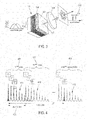
- the FIGURE 5 illustrates a masking file used for lithography of a wafer 500 intended to design the laser device 100 according to the present invention and incorporating a spatial filter on the top surface of the semiconductor element 111.
- Many types of patterns are designed on the wafer 500 with different dimensional characteristics. Some of them are bigger than others in order to optimize the selection of transverse modes, depending on the size of the beam and the pumping laser 110.
- these drawings are almost equivalent. They make it possible to filter various orders of transverse modes.
- FIGURE 6 illustrates an optical microscope image of metal masks in chromium 610, 620, 630, 640 according to the invention as well as the corresponding transverse Laguerre-Gauss modes obtained by simulation with such filters 615, 625, 635, 645 respectively.
- the images 6.a and 6.b illustrate metal masks 610, 620, 630, 640 for two different filtering orders of the transverse Laguerre-Gauss modes.
- the cross pattern 610, 630 and the flower-shaped pattern 620, 640 are equivalent, as can be seen in the images 6.c and 6.d respectively.
- the images 6.c and 6.d illustrate the corresponding transverse LG modes which can be obtained with these absorbent masks: the mask 610 and 620 makes it possible to filter the modes LG00 + LG02 (615 and 625) while the mask 630 and 640 are used to filter the LG00 + LG03 (635 and 645) modes.
- Laguerre-Gauss modes are designed based on certain physical parameters. By knowing the optical parameters of the cavity, the corresponding Laguerre-Gauss modes can be calculated. Several of these modes cannot achieve sufficient operation for laser emission because the Gaussian pump beam is focused at the center of the structure, thus only allowing (and thus selecting) the existence of low order transverse modes. For a given geometry of the mask, the losses can be calculated for each Laguerre-Gauss mode and the lowest losses should be obtained for the selected modes LG 00 and LG 02 for example. Thanks to their almost complementary transverse distributions, these two modes should coexist due to the burning of transverse spatial holes (“transverse spatial hole burning”).
- the present invention covers all the configurations for stabilizing / selecting at least two transverse modes: a mask may be able to select one, two or more than two transverse modes. As described below on FIGURE 8 , two masks 820, 830 can be combined so that each selects at least one different transverse mode.
- the mask is formed by depositing a 10 nm layer of chromium with a width of a few microns on the half-VeCSEL.
- the transverse dimensional characteristics are about a few microns, depending on the beam diameter, and, with regard to the longitudinal dimensions, the masks must be thin enough not to absorb transverse modes which one seeks to propagate to the inside the cavity. They must be thin enough to achieve light diffraction.
- a thickness of 10 nm is optimal for chromium for example, but it depends on the absorption coefficient of the material chosen. More generally, the thickness is less than the wavelength of the corresponding optical wave 107.
- the mask is deposited at a belly of the optical wave 107 which oscillates inside the optical cavity.
- the deposition material is not limiting in the present invention. Depending on the applications, the desired wavelength, the technologies and / or the desired performances, it is possible to deposit a metallic material, a doped semiconductor material, or a chemically etched material and / or a dielectric.
- the FIGURE 7 illustrates the implementation of such an absorbent mask 710 according to the invention, on the top surface 701 of a half-VeCSEL 111. Thanks to the absorption areas and the transmission areas, two transverse modes 720, 730 are selected and are - finally - stabilized inside the optical laser cavity thanks to the phenomenon known as the burning of transverse spatial holes (“transverse spatial hole burning”) in the gain region 104. These modes oscillate between the Bragg mirror 103 located inside the semiconductor element 111 and the second external concave mirror 106.
- FIG. 7 a diagram illustrates the propagation of the intensity of the field 740 inside the cavity: it shows the propagating wave inside the Bragg mirror and resonating through the active zone and the gain region 104 during d 'optical pumping.
- the FIGURE 8 illustrates a schematic view of a laser device 800 according to another embodiment of the invention with two masks metallic 820, 830. Each mask is deposited, one after the other.
- the Bragg mirror 103 is deposited on the substrate 102.
- the active area with the gain region 104 is deposited and lithographed on the Bragg mirror.
- a first mask 810 with a first pattern is deposited on the surface; in the example illustrated, this is a chrome mask whose thickness is 10 nm.
- a spacer 820 is deposited with a thickness which depends on the wavelength. In the example illustrated, its thickness is equal to half the wavelength.
- a second metal absorbent mask 830 with a second pattern which may be different from the first is deposited on the spacer.
- each mask is located on a belly of the optical wave 107 which is generated by the present laser device.
- the FIGURE 9 shows a view of the far-field intensity of the laser according to the invention, with an integrated metallic absorbent mask.
- the FIGURE 9 also illustrates the coexistence of the two Laguerre-Gauss modes.
- the FIGURE 10 illustrates the optical spectrum of the laser according to the invention. It shows that the laser according to the present invention provides dual-frequency operation, illustrated by the two peaks plotted and exhibiting a frequency difference between the two modes of 162 GHz. By changing the patterns of the absorbent masks, it is possible to change the beat frequency up to 450 GHz.
- the FIGURE 11 illustrates laser output power as a function of optical pump power.
- the output power of the laser is linear with a first slope up to a threshold value which corresponds to the second transverse mode and from which the slope of the power of output of the laser increases: the efficiency of the laser according to the invention increases when the second mode appears.
- the threshold value of the pumping power is, for the first mode, around 150 mW, and the threshold value for the second mode is around 250 mW.
- the FIGURE 12 is a laser device 100 according to the invention with a diffractive mask on the semiconductor element 111 in accordance with the previous description. It consists of a single layer of Si 3 N 4 1210 completed by a 2D network of holes 1220 of diameters d arranged along a square grid of period a. The diameter of the holes can be constant or variable, depending on the desired effects.
- the single layer of Si 3 N 4 is a photonic crystal mirror and deposited on the top surface of the half-VeCSEL 111, as for absorbent masks. The principle is close to that of absorption masks but it is based on diffraction effects instead of absorption effects. Thus, the light is diffracted in order to diffract the Laguerre-Gauss modes which are not desired.
- the FIGURE 13 illustrates another diffractive mask pattern which introduces losses on the optical wave 107 which oscillates inside the laser cavity.
- the diffractive mask 1310 according to this embodiment is composed of four diffraction gratings 1320, 1340, 1360, 1380 etched on the two axes of symmetry of the spatial filter 1310.
- the pitch is 1 ⁇ m and the size of each mark is 200 nm.
- Two modes are selected thanks to this diffractive photonic crystal type mask: the main mode TEMoo 1305 represented by a circular line centered on the mask and the LG 02 mode represented by a concave and closed curve (1301 to 1304) at each corner of the mask .
- the typical thickness of the dielectric deposit on which the diffractive structures are etched is between about half the wavelength and one-eighth of the wavelength.
- Diffractive masks can be made by certain microelectronic techniques, such as absorbent masks.
- the shaping of the intensity of the optical wave 107 which resonates inside the laser cavity is no longer carried out by an absorption mask; it is now carried out by optical pumping.
- the optical pumping is completely homogeneous over the zone corresponding to the desired beam - profile of either Gaussian or top hat type - on the active surface of the semiconductor element on which pumping is carried out.
- the spatial transverse filter is mounted on the optical components which focus the pumping laser beam 110 on the active surface of the semiconductor element, in order to decrease its intensity in certain zones, called absorption zones, and to allow transmission. light in certain other areas, called transmission areas.
- the shape and location of these areas on the pump laser beam 110 are arranged to be projected onto the active surface onto the semiconductor element, and so that they overlap with the transverse Laguerre-Gauss modes that the we are trying to intercept. Only those corresponding to the transverse Laguerre-Gauss modes which one seeks to select will be effectively pumped by this pumping laser of non-homogeneous intensity.
- another optical pump shaping technique can be achieved by focusing two elliptical pump beams (the two ellipses being transverse to each other) on the chip. semiconductor to produce a so-called pumping area similar in shape to that of a petal.
- the FIGURE 14 illustrates the THz spectrum of the dual-frequency Laguerre-Gauss VeCSEL by photo-coupling and the temporal evolution of its intensity of fashion. It shows the simultaneous laser generation of two mutually coherent optical waves (i.e. showing low relative phase noise) inside a single VeCSEL cavity, in continuous wave operation at 300K and power. moderate (35 mW).
- the FIGURE 14 thus illustrates the generation of coherent THz wave by photo-coupling of the two-frequency Laguerre-Gauss VeCSEL in a UTC photodiode, and confirms the theoretical study of the laser dynamics, showing the simultaneous emission of the two LG modes, in steady state , dual frequency VeCSEL.
- the FIGURE 15 describes a diagram of a spectral filter making it possible to shape the phase profile of the optical wave oscillating in the optical cavity, in a complementary manner to the means for selecting the at least two transverse modes.
- Diagram (a) illustrates an optical cavity in which two transverse modes have been selected (means not shown) and incorporating a spectral filter in order to adjust the frequency difference between the two modes
- diagram (b) illustrates a front view of said spectral filter
- diagram (c) illustrates on the one hand the passband of such a filter, for the two transverse oscillating modes in the optical cavity and on the other hand the gain of the amplifying medium.
- the device according to the invention can comprise between the two mirrors M1 and M2 forming the optical cavity - in a complementary manner to the means for selecting at least two transverse modes not shown - a spectral filter absorption and / or an amplifying spectral filter 1503 arranged to generate a phase shift between the two transverse modes and thus grant the frequency difference between the two oscillating transverse modes ( ⁇ 1, ⁇ 2) inside the cavity.
- the intensity of the oscillating transverse modes inside the cavity is illustrated in 1504.
- This filtering can for example be obtained using a Lyot or Farby-Perot filter comprising a gain medium and / or a loss medium.
- the adjustment of the cavity can thus be achieved by adjusting said filter so that each oscillating transverse mode ⁇ 1, ⁇ 2 passes through a different optical length through the filter.
- the spectral filter is designed to have a refractive index, or even a non-uniform transverse optical length so as to generate a phase shift between the two oscillating transverse modes.
- such a filter can be obtained using a Bragg mirror (1-10 pairs) with low reflectivity and located on the structure of the semiconductor element (ie the VCSEL by example).
- a Bragg mirror (1-10 pairs) with low reflectivity and located on the structure of the semiconductor element (ie the VCSEL by example).
- Such a mirror can be produced by well-known microelectronic deposition processes.
- Such a spectral filter advantageously makes it possible to obtain a “factory setting” of the frequency difference between the two oscillating transverse modes.
- such a spectral filter can also be dynamic in order to provide a means of controlling the frequency difference between the two oscillating transverse modes inside the cavity. It may for example be a matrix of controllable liquid crystal pixels.
- the adjustment of the characteristic dimensions of such a mirror makes it possible to control the refractive index “perceived” by each transverse mode oscillating in the cavity; and it is possible, for example, by increasing the optical thickness of the material crossed by a first mode, relative to that crossed by the second mode, to very precisely control the frequency deviation desired for the device according to the invention. More particularly, an attempt will be made to modify the values of refractive indices (and therefore of thickness) of the central zone of said filter with respect to the peripheral zone. For example, it is possible to etch on the upper surface of the Bragg mirror a phase-shifting overlayer with a thickness typically less than ⁇ / 2 on one of the transverse modes with respect to the other transverse mode.
- phase-shifting structure for example a photonic crystal or a meta-material whose refractive index is spatially controlled by the characteristic dimensions of a network.
- a phase-shifting structure for example a photonic crystal or a meta-material whose refractive index is spatially controlled by the characteristic dimensions of a network.
- it may be a two-dimensional network of holes whose diameters and periodicity evolve according to a particular profile which determines the phase profile of the transverse modes. It is therefore possible to produce "on demand" particular phase profiles, and in particular continuous, making it possible to obtain very fine adjustments between the modes.
- FIGURE 16 schematically illustrates an embodiment of the device according to the invention, in which a non-uniform gain medium makes it possible to adjust the frequency difference between the two transverse modes selected by said device, the means making it possible to select the two transverse modes n ' being not represented.
- Diagram (a) illustrates an optical cavity integrating a non-uniform gain medium
- diagram (b) illustrates a front view of said gain medium
- diagram (c) illustrates the passband of the gain medium.
- the device according to the invention can comprise between the two mirrors M1 and M2 forming the optical cavity at least one gain medium 1601, 1602 arranged to match the frequency difference between the two oscillating transverse modes ( ⁇ 1, ⁇ 2) inside the cavity.
- the intensity of the oscillating transverse modes inside the cavity is illustrated in 1603.
- such an adjustment can be obtained by means of a non-uniform transverse distribution of the losses at the level of the gain medium, and / or by a non-uniform distribution of the carriers of charge in said gain medium.
- the intensity of the emission length of the gain varies transversely and makes it possible to adjust the frequency difference between the two transverse modes.
- the device according to the invention can comprise at least one non-uniform loss mask transversely between the two modes in order to adjust the frequency difference between the two modes.
Landscapes
- Physics & Mathematics (AREA)
- Electromagnetism (AREA)
- Optics & Photonics (AREA)
- Condensed Matter Physics & Semiconductors (AREA)
- General Physics & Mathematics (AREA)
- Engineering & Computer Science (AREA)
- Plasma & Fusion (AREA)
- Chemical & Material Sciences (AREA)
- Crystallography & Structural Chemistry (AREA)
- Semiconductor Lasers (AREA)
- Optical Modulation, Optical Deflection, Nonlinear Optics, Optical Demodulation, Optical Logic Elements (AREA)
Applications Claiming Priority (2)
| Application Number | Priority Date | Filing Date | Title |
|---|---|---|---|
| FR1402058A FR3025948B1 (fr) | 2014-09-15 | 2014-09-15 | Dispositif laser a cavite externe verticale a emission par la surface a double frequence pour la generation de thz et procede de generation de thz |
| PCT/EP2015/071139 WO2016041993A1 (fr) | 2014-09-15 | 2015-09-15 | Dispositif laser a cavite externe verticale a emission par la surface a double frequences, pour la generation de thz et procede de generation de thz |
Publications (2)
| Publication Number | Publication Date |
|---|---|
| EP3195428A1 EP3195428A1 (fr) | 2017-07-26 |
| EP3195428B1 true EP3195428B1 (fr) | 2020-07-22 |
Family
ID=52684255
Family Applications (1)
| Application Number | Title | Priority Date | Filing Date |
|---|---|---|---|
| EP15775115.7A Active EP3195428B1 (fr) | 2014-09-15 | 2015-09-15 | Dispositif laser a cavite externe verticale a emission par la surface a double frequences, pour la generation de thz et procede de generation de thz. |
Country Status (5)
| Country | Link |
|---|---|
| US (1) | US10141718B2 (https=) |
| EP (1) | EP3195428B1 (https=) |
| JP (1) | JP6805149B2 (https=) |
| FR (1) | FR3025948B1 (https=) |
| WO (1) | WO2016041993A1 (https=) |
Families Citing this family (10)
| Publication number | Priority date | Publication date | Assignee | Title |
|---|---|---|---|---|
| DE102017129173A1 (de) * | 2017-12-07 | 2019-06-13 | Osram Opto Semiconductors Gmbh | Strahlungsquelle zur Emission von Terahertz-Strahlung |
| FR3078834B1 (fr) * | 2018-03-08 | 2020-03-27 | Commissariat A L'energie Atomique Et Aux Energies Alternatives | Dispositif d’emission lumineuse comportant au moins un vcsel et une lentille de diffusion |
| CN108535891B (zh) * | 2018-04-11 | 2020-01-10 | 雄安华讯方舟科技有限公司 | 一种太赫兹波波前相位调制方法 |
| CN109031241B (zh) * | 2018-06-27 | 2021-03-23 | 森思泰克河北科技有限公司 | 激光雷达发射系统 |
| CN109586146B (zh) * | 2019-01-10 | 2019-10-15 | 北京邮电大学 | 一种太赫兹波发生器 |
| KR102745348B1 (ko) | 2019-09-23 | 2024-12-23 | 삼성전자주식회사 | 광 변조 소자, 이를 포함하는 빔 스티어링 장치 및 빔 스티어링 장치를 포함하는 전자 장치 |
| US11588298B2 (en) | 2020-06-23 | 2023-02-21 | Hewlett Packard Enterprise Development Lp | Coupled-cavity VCSELs for enhanced modulation bandwidth |
| US12212113B2 (en) | 2022-03-31 | 2025-01-28 | Xemed Llc | Gaseous laser systems with edge-defining element and related techniques |
| US12548968B2 (en) | 2022-03-31 | 2026-02-10 | Xemed Llc | Gaseous laser systems with edge-defining element and related techniques |
| US11855406B2 (en) * | 2022-03-31 | 2023-12-26 | Xemed Llc | Gaseous laser systems with edge-defining element and related techniques |
Family Cites Families (10)
| Publication number | Priority date | Publication date | Assignee | Title |
|---|---|---|---|---|
| US6711203B1 (en) | 2000-09-22 | 2004-03-23 | Blueleaf, Inc. | Optical transmitter comprising a stepwise tunable laser |
| US6658034B2 (en) | 2000-12-13 | 2003-12-02 | Picarro, Inc. | Surface-emitting semiconductor laser |
| JP4232475B2 (ja) * | 2003-02-03 | 2009-03-04 | ソニー株式会社 | 面発光レーザ素子 |
| DE10339980B4 (de) * | 2003-08-29 | 2011-01-05 | Osram Opto Semiconductors Gmbh | Halbleiterlaser mit reduzierter Verlustwärme |
| JP4944788B2 (ja) * | 2004-11-29 | 2012-06-06 | アライト フォトニックス エイピーエス | 単一モードフォトニック結晶vcsel |
| KR100657963B1 (ko) * | 2005-06-28 | 2006-12-14 | 삼성전자주식회사 | 고출력 수직외부공진형 표면발광 레이저 |
| WO2008135903A2 (en) * | 2007-05-07 | 2008-11-13 | Philips Intellectual Property & Standards Gmbh | Laser sensor for self-mixing interferometry with increased detection range |
| DE102008021791A1 (de) * | 2008-04-30 | 2009-11-26 | ARIZONA BOARD OF REGENTS, on behalf of THE UNIVERSITY OF ARIZONA, Tucson | Laserbasierte Quelle für Terahertz- und Millimeterwellen |
| EP2369696A1 (en) * | 2010-03-23 | 2011-09-28 | ETH Zurich | Surface-Emitting semiconductor laser and method of manufacture thereof |
| WO2012035621A1 (ja) * | 2010-09-14 | 2012-03-22 | キヤノン株式会社 | フォトニック結晶面発光レーザ、該レーザを用いたレーザアレイ、該レーザアレイを用いた画像形成装置 |
-
2014
- 2014-09-15 FR FR1402058A patent/FR3025948B1/fr active Active
-
2015
- 2015-09-15 EP EP15775115.7A patent/EP3195428B1/fr active Active
- 2015-09-15 US US15/511,199 patent/US10141718B2/en not_active Expired - Fee Related
- 2015-09-15 JP JP2017534003A patent/JP6805149B2/ja not_active Expired - Fee Related
- 2015-09-15 WO PCT/EP2015/071139 patent/WO2016041993A1/fr not_active Ceased
Non-Patent Citations (1)
| Title |
|---|
| None * |
Also Published As
| Publication number | Publication date |
|---|---|
| JP2017528008A (ja) | 2017-09-21 |
| US10141718B2 (en) | 2018-11-27 |
| WO2016041993A1 (fr) | 2016-03-24 |
| FR3025948A1 (https=) | 2016-03-18 |
| EP3195428A1 (fr) | 2017-07-26 |
| FR3025948B1 (fr) | 2018-03-16 |
| US20170256913A1 (en) | 2017-09-07 |
| JP6805149B2 (ja) | 2020-12-23 |
Similar Documents
| Publication | Publication Date | Title |
|---|---|---|
| EP3195428B1 (fr) | Dispositif laser a cavite externe verticale a emission par la surface a double frequences, pour la generation de thz et procede de generation de thz. | |
| CN107258040B (zh) | 具有携带受控轨道角动量的光束的激光装置 | |
| US9065246B2 (en) | Infrared laser | |
| EP0821451A1 (fr) | Microlaser solide, à pompage optique par laser semi-conducteur à cavité verticale | |
| JP6895903B2 (ja) | 半導体レーザ素子、回折格子構造、および回折格子 | |
| WO2019002763A1 (fr) | Source laser à semi-conducteur | |
| EP1125347B1 (fr) | Filtres auto-adaptes pour l'affinement de l'emission laser | |
| EP3211736B1 (en) | Semiconductor laser diode and method of manufacture thereof | |
| WO2012101367A1 (fr) | Cavite laser bifrequences accordable et procede de reglage de la difference de frequence entre une onde ordinaire et une onde extraordinaire d'un laser bifrequences | |
| FR2842037A1 (fr) | Laser dfb a reflecteur distribue a bande photonique interdite | |
| EP3140888B1 (fr) | Laser a etat solide faible bruit | |
| EP4053603A1 (fr) | Emetteur optoelectronique a balayage angulaire rapide | |
| Chen et al. | Optically pumped distributed feedback laser from organo-lead iodide perovskite thin films | |
| EP1031172A1 (fr) | Realisation d'emetteurs hyperfrequences et applications aux radars et aux telecommunications | |
| Büttner et al. | Folded diffractive laser resonators with user-defined fundamental mode | |
| FR2825524A1 (fr) | Laser amplificateur a cavite verticale | |
| FR3111023A1 (fr) | Dispositif de génération de trains d'impulsions radiofréquences | |
| WO2017202815A1 (fr) | Reseau de lasers a cascade quantique a antiguidage enterre dans un materiau de type iv et a emission monolobe | |
| FR3009628A1 (fr) | Reflecteur optique accordable en longuer d'onde |
Legal Events
| Date | Code | Title | Description |
|---|---|---|---|
| STAA | Information on the status of an ep patent application or granted ep patent |
Free format text: STATUS: THE INTERNATIONAL PUBLICATION HAS BEEN MADE |
|
| PUAI | Public reference made under article 153(3) epc to a published international application that has entered the european phase |
Free format text: ORIGINAL CODE: 0009012 |
|
| STAA | Information on the status of an ep patent application or granted ep patent |
Free format text: STATUS: REQUEST FOR EXAMINATION WAS MADE |
|
| 17P | Request for examination filed |
Effective date: 20170412 |
|
| AK | Designated contracting states |
Kind code of ref document: A1 Designated state(s): AL AT BE BG CH CY CZ DE DK EE ES FI FR GB GR HR HU IE IS IT LI LT LU LV MC MK MT NL NO PL PT RO RS SE SI SK SM TR |
|
| AX | Request for extension of the european patent |
Extension state: BA ME |
|
| STAA | Information on the status of an ep patent application or granted ep patent |
Free format text: STATUS: EXAMINATION IS IN PROGRESS |
|
| 17Q | First examination report despatched |
Effective date: 20190730 |
|
| GRAP | Despatch of communication of intention to grant a patent |
Free format text: ORIGINAL CODE: EPIDOSNIGR1 |
|
| STAA | Information on the status of an ep patent application or granted ep patent |
Free format text: STATUS: GRANT OF PATENT IS INTENDED |
|
| INTG | Intention to grant announced |
Effective date: 20200214 |
|
| RIN1 | Information on inventor provided before grant (corrected) |
Inventor name: SELLAHI, MOHAMED Inventor name: PAQUET, ROMAIN Inventor name: BLIN, STEPHANE Inventor name: BEAUDOIN, GREGOIRE Inventor name: SAGNES, ISABELLE Inventor name: GARNACHE-CREUILLOT, ARNAUD Inventor name: MYARA, MIKHAEL |
|
| GRAS | Grant fee paid |
Free format text: ORIGINAL CODE: EPIDOSNIGR3 |
|
| GRAA | (expected) grant |
Free format text: ORIGINAL CODE: 0009210 |
|
| STAA | Information on the status of an ep patent application or granted ep patent |
Free format text: STATUS: THE PATENT HAS BEEN GRANTED |
|
| AK | Designated contracting states |
Kind code of ref document: B1 Designated state(s): AL AT BE BG CH CY CZ DE DK EE ES FI FR GB GR HR HU IE IS IT LI LT LU LV MC MK MT NL NO PL PT RO RS SE SI SK SM TR |
|
| AX | Request for extension of the european patent |
Extension state: BA ME |
|
| REG | Reference to a national code |
Ref country code: GB Ref legal event code: FG4D Free format text: NOT ENGLISH |
|
| REG | Reference to a national code |
Ref country code: CH Ref legal event code: EP |
|
| REG | Reference to a national code |
Ref country code: DE Ref legal event code: R096 Ref document number: 602015056194 Country of ref document: DE |
|
| REG | Reference to a national code |
Ref country code: AT Ref legal event code: REF Ref document number: 1294283 Country of ref document: AT Kind code of ref document: T Effective date: 20200815 |
|
| REG | Reference to a national code |
Ref country code: IE Ref legal event code: FG4D Free format text: LANGUAGE OF EP DOCUMENT: FRENCH |
|
| REG | Reference to a national code |
Ref country code: CH Ref legal event code: NV Representative=s name: DENNEMEYER AG, CH |
|
| PGFP | Annual fee paid to national office [announced via postgrant information from national office to epo] |
Ref country code: GB Payment date: 20200921 Year of fee payment: 6 |
|
| REG | Reference to a national code |
Ref country code: SE Ref legal event code: TRGR |
|
| PGFP | Annual fee paid to national office [announced via postgrant information from national office to epo] |
Ref country code: CH Payment date: 20200921 Year of fee payment: 6 |
|
| REG | Reference to a national code |
Ref country code: LT Ref legal event code: MG4D |
|
| REG | Reference to a national code |
Ref country code: AT Ref legal event code: MK05 Ref document number: 1294283 Country of ref document: AT Kind code of ref document: T Effective date: 20200722 |
|
| PG25 | Lapsed in a contracting state [announced via postgrant information from national office to epo] |
Ref country code: FI Free format text: LAPSE BECAUSE OF FAILURE TO SUBMIT A TRANSLATION OF THE DESCRIPTION OR TO PAY THE FEE WITHIN THE PRESCRIBED TIME-LIMIT Effective date: 20200722 Ref country code: AT Free format text: LAPSE BECAUSE OF FAILURE TO SUBMIT A TRANSLATION OF THE DESCRIPTION OR TO PAY THE FEE WITHIN THE PRESCRIBED TIME-LIMIT Effective date: 20200722 Ref country code: LT Free format text: LAPSE BECAUSE OF FAILURE TO SUBMIT A TRANSLATION OF THE DESCRIPTION OR TO PAY THE FEE WITHIN THE PRESCRIBED TIME-LIMIT Effective date: 20200722 Ref country code: GR Free format text: LAPSE BECAUSE OF FAILURE TO SUBMIT A TRANSLATION OF THE DESCRIPTION OR TO PAY THE FEE WITHIN THE PRESCRIBED TIME-LIMIT Effective date: 20201023 Ref country code: HR Free format text: LAPSE BECAUSE OF FAILURE TO SUBMIT A TRANSLATION OF THE DESCRIPTION OR TO PAY THE FEE WITHIN THE PRESCRIBED TIME-LIMIT Effective date: 20200722 Ref country code: NO Free format text: LAPSE BECAUSE OF FAILURE TO SUBMIT A TRANSLATION OF THE DESCRIPTION OR TO PAY THE FEE WITHIN THE PRESCRIBED TIME-LIMIT Effective date: 20201022 Ref country code: ES Free format text: LAPSE BECAUSE OF FAILURE TO SUBMIT A TRANSLATION OF THE DESCRIPTION OR TO PAY THE FEE WITHIN THE PRESCRIBED TIME-LIMIT Effective date: 20200722 Ref country code: PT Free format text: LAPSE BECAUSE OF FAILURE TO SUBMIT A TRANSLATION OF THE DESCRIPTION OR TO PAY THE FEE WITHIN THE PRESCRIBED TIME-LIMIT Effective date: 20201123 Ref country code: BG Free format text: LAPSE BECAUSE OF FAILURE TO SUBMIT A TRANSLATION OF THE DESCRIPTION OR TO PAY THE FEE WITHIN THE PRESCRIBED TIME-LIMIT Effective date: 20201022 |
|
| PG25 | Lapsed in a contracting state [announced via postgrant information from national office to epo] |
Ref country code: PL Free format text: LAPSE BECAUSE OF FAILURE TO SUBMIT A TRANSLATION OF THE DESCRIPTION OR TO PAY THE FEE WITHIN THE PRESCRIBED TIME-LIMIT Effective date: 20200722 Ref country code: LV Free format text: LAPSE BECAUSE OF FAILURE TO SUBMIT A TRANSLATION OF THE DESCRIPTION OR TO PAY THE FEE WITHIN THE PRESCRIBED TIME-LIMIT Effective date: 20200722 Ref country code: RS Free format text: LAPSE BECAUSE OF FAILURE TO SUBMIT A TRANSLATION OF THE DESCRIPTION OR TO PAY THE FEE WITHIN THE PRESCRIBED TIME-LIMIT Effective date: 20200722 Ref country code: IS Free format text: LAPSE BECAUSE OF FAILURE TO SUBMIT A TRANSLATION OF THE DESCRIPTION OR TO PAY THE FEE WITHIN THE PRESCRIBED TIME-LIMIT Effective date: 20201122 |
|
| PG25 | Lapsed in a contracting state [announced via postgrant information from national office to epo] |
Ref country code: NL Free format text: LAPSE BECAUSE OF FAILURE TO SUBMIT A TRANSLATION OF THE DESCRIPTION OR TO PAY THE FEE WITHIN THE PRESCRIBED TIME-LIMIT Effective date: 20200722 |
|
| PGFP | Annual fee paid to national office [announced via postgrant information from national office to epo] |
Ref country code: SE Payment date: 20200925 Year of fee payment: 6 |
|
| REG | Reference to a national code |
Ref country code: DE Ref legal event code: R097 Ref document number: 602015056194 Country of ref document: DE |
|
| PG25 | Lapsed in a contracting state [announced via postgrant information from national office to epo] |
Ref country code: MC Free format text: LAPSE BECAUSE OF FAILURE TO SUBMIT A TRANSLATION OF THE DESCRIPTION OR TO PAY THE FEE WITHIN THE PRESCRIBED TIME-LIMIT Effective date: 20200722 Ref country code: SM Free format text: LAPSE BECAUSE OF FAILURE TO SUBMIT A TRANSLATION OF THE DESCRIPTION OR TO PAY THE FEE WITHIN THE PRESCRIBED TIME-LIMIT Effective date: 20200722 Ref country code: RO Free format text: LAPSE BECAUSE OF FAILURE TO SUBMIT A TRANSLATION OF THE DESCRIPTION OR TO PAY THE FEE WITHIN THE PRESCRIBED TIME-LIMIT Effective date: 20200722 Ref country code: EE Free format text: LAPSE BECAUSE OF FAILURE TO SUBMIT A TRANSLATION OF THE DESCRIPTION OR TO PAY THE FEE WITHIN THE PRESCRIBED TIME-LIMIT Effective date: 20200722 Ref country code: IT Free format text: LAPSE BECAUSE OF FAILURE TO SUBMIT A TRANSLATION OF THE DESCRIPTION OR TO PAY THE FEE WITHIN THE PRESCRIBED TIME-LIMIT Effective date: 20200722 Ref country code: CZ Free format text: LAPSE BECAUSE OF FAILURE TO SUBMIT A TRANSLATION OF THE DESCRIPTION OR TO PAY THE FEE WITHIN THE PRESCRIBED TIME-LIMIT Effective date: 20200722 Ref country code: DK Free format text: LAPSE BECAUSE OF FAILURE TO SUBMIT A TRANSLATION OF THE DESCRIPTION OR TO PAY THE FEE WITHIN THE PRESCRIBED TIME-LIMIT Effective date: 20200722 |
|
| PLBE | No opposition filed within time limit |
Free format text: ORIGINAL CODE: 0009261 |
|
| STAA | Information on the status of an ep patent application or granted ep patent |
Free format text: STATUS: NO OPPOSITION FILED WITHIN TIME LIMIT |
|
| PG25 | Lapsed in a contracting state [announced via postgrant information from national office to epo] |
Ref country code: AL Free format text: LAPSE BECAUSE OF FAILURE TO SUBMIT A TRANSLATION OF THE DESCRIPTION OR TO PAY THE FEE WITHIN THE PRESCRIBED TIME-LIMIT Effective date: 20200722 |
|
| VS25 | Lapsed in a validation state [announced via postgrant information from nat. office to epo] |
Ref country code: MA Free format text: LAPSE BECAUSE OF FAILURE TO SUBMIT A TRANSLATION OF THE DESCRIPTION OR TO PAY THE FEE WITHIN THE PRESCRIBED TIME-LIMIT Effective date: 20200722 |
|
| REG | Reference to a national code |
Ref country code: BE Ref legal event code: MM Effective date: 20200930 |
|
| 26N | No opposition filed |
Effective date: 20210423 |
|
| PG25 | Lapsed in a contracting state [announced via postgrant information from national office to epo] |
Ref country code: LU Free format text: LAPSE BECAUSE OF NON-PAYMENT OF DUE FEES Effective date: 20200915 Ref country code: SK Free format text: LAPSE BECAUSE OF FAILURE TO SUBMIT A TRANSLATION OF THE DESCRIPTION OR TO PAY THE FEE WITHIN THE PRESCRIBED TIME-LIMIT Effective date: 20200722 |
|
| PG25 | Lapsed in a contracting state [announced via postgrant information from national office to epo] |
Ref country code: SI Free format text: LAPSE BECAUSE OF FAILURE TO SUBMIT A TRANSLATION OF THE DESCRIPTION OR TO PAY THE FEE WITHIN THE PRESCRIBED TIME-LIMIT Effective date: 20200722 Ref country code: IE Free format text: LAPSE BECAUSE OF NON-PAYMENT OF DUE FEES Effective date: 20200915 Ref country code: BE Free format text: LAPSE BECAUSE OF NON-PAYMENT OF DUE FEES Effective date: 20200930 |
|
| REG | Reference to a national code |
Ref country code: NL Ref legal event code: MP Effective date: 20200722 |
|
| REG | Reference to a national code |
Ref country code: SE Ref legal event code: EUG |
|
| REG | Reference to a national code |
Ref country code: CH Ref legal event code: PL |
|
| GBPC | Gb: european patent ceased through non-payment of renewal fee |
Effective date: 20210915 |
|
| PG25 | Lapsed in a contracting state [announced via postgrant information from national office to epo] |
Ref country code: TR Free format text: LAPSE BECAUSE OF FAILURE TO SUBMIT A TRANSLATION OF THE DESCRIPTION OR TO PAY THE FEE WITHIN THE PRESCRIBED TIME-LIMIT Effective date: 20200722 Ref country code: MT Free format text: LAPSE BECAUSE OF FAILURE TO SUBMIT A TRANSLATION OF THE DESCRIPTION OR TO PAY THE FEE WITHIN THE PRESCRIBED TIME-LIMIT Effective date: 20200722 Ref country code: CY Free format text: LAPSE BECAUSE OF FAILURE TO SUBMIT A TRANSLATION OF THE DESCRIPTION OR TO PAY THE FEE WITHIN THE PRESCRIBED TIME-LIMIT Effective date: 20200722 |
|
| PG25 | Lapsed in a contracting state [announced via postgrant information from national office to epo] |
Ref country code: MK Free format text: LAPSE BECAUSE OF FAILURE TO SUBMIT A TRANSLATION OF THE DESCRIPTION OR TO PAY THE FEE WITHIN THE PRESCRIBED TIME-LIMIT Effective date: 20200722 |
|
| PG25 | Lapsed in a contracting state [announced via postgrant information from national office to epo] |
Ref country code: SE Free format text: LAPSE BECAUSE OF NON-PAYMENT OF DUE FEES Effective date: 20210916 Ref country code: GB Free format text: LAPSE BECAUSE OF NON-PAYMENT OF DUE FEES Effective date: 20210915 |
|
| PG25 | Lapsed in a contracting state [announced via postgrant information from national office to epo] |
Ref country code: LI Free format text: LAPSE BECAUSE OF NON-PAYMENT OF DUE FEES Effective date: 20210930 Ref country code: CH Free format text: LAPSE BECAUSE OF NON-PAYMENT OF DUE FEES Effective date: 20210930 |
|
| PGFP | Annual fee paid to national office [announced via postgrant information from national office to epo] |
Ref country code: DE Payment date: 20241016 Year of fee payment: 10 |
|
| PGFP | Annual fee paid to national office [announced via postgrant information from national office to epo] |
Ref country code: FR Payment date: 20250926 Year of fee payment: 11 |