EP3188274A1 - Organic light-emitting display device and method of fabricating the same - Google Patents
Organic light-emitting display device and method of fabricating the same Download PDFInfo
- Publication number
- EP3188274A1 EP3188274A1 EP16187892.1A EP16187892A EP3188274A1 EP 3188274 A1 EP3188274 A1 EP 3188274A1 EP 16187892 A EP16187892 A EP 16187892A EP 3188274 A1 EP3188274 A1 EP 3188274A1
- Authority
- EP
- European Patent Office
- Prior art keywords
- substrate
- buffer layer
- forming
- layer
- auxiliary electrode
- Prior art date
- Legal status (The legal status is an assumption and is not a legal conclusion. Google has not performed a legal analysis and makes no representation as to the accuracy of the status listed.)
- Granted
Links
Images




Classifications
-
- H—ELECTRICITY
- H10—SEMICONDUCTOR DEVICES; ELECTRIC SOLID-STATE DEVICES NOT OTHERWISE PROVIDED FOR
- H10D—INORGANIC ELECTRIC SEMICONDUCTOR DEVICES
- H10D86/00—Integrated devices formed in or on insulating or conducting substrates, e.g. formed in silicon-on-insulator [SOI] substrates or on stainless steel or glass substrates
- H10D86/40—Integrated devices formed in or on insulating or conducting substrates, e.g. formed in silicon-on-insulator [SOI] substrates or on stainless steel or glass substrates characterised by multiple TFTs
- H10D86/411—Integrated devices formed in or on insulating or conducting substrates, e.g. formed in silicon-on-insulator [SOI] substrates or on stainless steel or glass substrates characterised by multiple TFTs characterised by materials, geometry or structure of the substrates
-
- H—ELECTRICITY
- H10—SEMICONDUCTOR DEVICES; ELECTRIC SOLID-STATE DEVICES NOT OTHERWISE PROVIDED FOR
- H10D—INORGANIC ELECTRIC SEMICONDUCTOR DEVICES
- H10D86/00—Integrated devices formed in or on insulating or conducting substrates, e.g. formed in silicon-on-insulator [SOI] substrates or on stainless steel or glass substrates
- H10D86/40—Integrated devices formed in or on insulating or conducting substrates, e.g. formed in silicon-on-insulator [SOI] substrates or on stainless steel or glass substrates characterised by multiple TFTs
- H10D86/441—Interconnections, e.g. scanning lines
-
- H—ELECTRICITY
- H10—SEMICONDUCTOR DEVICES; ELECTRIC SOLID-STATE DEVICES NOT OTHERWISE PROVIDED FOR
- H10K—ORGANIC ELECTRIC SOLID-STATE DEVICES
- H10K59/00—Integrated devices, or assemblies of multiple devices, comprising at least one organic light-emitting element covered by group H10K50/00
- H10K59/10—OLED displays
- H10K59/12—Active-matrix OLED [AMOLED] displays
- H10K59/121—Active-matrix OLED [AMOLED] displays characterised by the geometry or disposition of pixel elements
- H10K59/1213—Active-matrix OLED [AMOLED] displays characterised by the geometry or disposition of pixel elements the pixel elements being TFTs
-
- H—ELECTRICITY
- H10—SEMICONDUCTOR DEVICES; ELECTRIC SOLID-STATE DEVICES NOT OTHERWISE PROVIDED FOR
- H10K—ORGANIC ELECTRIC SOLID-STATE DEVICES
- H10K59/00—Integrated devices, or assemblies of multiple devices, comprising at least one organic light-emitting element covered by group H10K50/00
- H10K59/10—OLED displays
- H10K59/12—Active-matrix OLED [AMOLED] displays
- H10K59/123—Connection of the pixel electrodes to the thin film transistors [TFT]
-
- H—ELECTRICITY
- H10—SEMICONDUCTOR DEVICES; ELECTRIC SOLID-STATE DEVICES NOT OTHERWISE PROVIDED FOR
- H10K—ORGANIC ELECTRIC SOLID-STATE DEVICES
- H10K59/00—Integrated devices, or assemblies of multiple devices, comprising at least one organic light-emitting element covered by group H10K50/00
- H10K59/10—OLED displays
- H10K59/12—Active-matrix OLED [AMOLED] displays
- H10K59/126—Shielding, e.g. light-blocking means over the TFTs
-
- H—ELECTRICITY
- H10—SEMICONDUCTOR DEVICES; ELECTRIC SOLID-STATE DEVICES NOT OTHERWISE PROVIDED FOR
- H10K—ORGANIC ELECTRIC SOLID-STATE DEVICES
- H10K59/00—Integrated devices, or assemblies of multiple devices, comprising at least one organic light-emitting element covered by group H10K50/00
- H10K59/10—OLED displays
- H10K59/12—Active-matrix OLED [AMOLED] displays
- H10K59/131—Interconnections, e.g. wiring lines or terminals
-
- H—ELECTRICITY
- H10—SEMICONDUCTOR DEVICES; ELECTRIC SOLID-STATE DEVICES NOT OTHERWISE PROVIDED FOR
- H10K—ORGANIC ELECTRIC SOLID-STATE DEVICES
- H10K59/00—Integrated devices, or assemblies of multiple devices, comprising at least one organic light-emitting element covered by group H10K50/00
- H10K59/80—Constructional details
- H10K59/805—Electrodes
- H10K59/8052—Cathodes
- H10K59/80522—Cathodes combined with auxiliary electrodes
-
- H—ELECTRICITY
- H10—SEMICONDUCTOR DEVICES; ELECTRIC SOLID-STATE DEVICES NOT OTHERWISE PROVIDED FOR
- H10W—GENERIC PACKAGES, INTERCONNECTIONS, CONNECTORS OR OTHER CONSTRUCTIONAL DETAILS OF DEVICES COVERED BY CLASS H10
- H10W46/00—Marks applied to devices, e.g. for alignment or identification
-
- H—ELECTRICITY
- H10—SEMICONDUCTOR DEVICES; ELECTRIC SOLID-STATE DEVICES NOT OTHERWISE PROVIDED FOR
- H10D—INORGANIC ELECTRIC SEMICONDUCTOR DEVICES
- H10D86/00—Integrated devices formed in or on insulating or conducting substrates, e.g. formed in silicon-on-insulator [SOI] substrates or on stainless steel or glass substrates
- H10D86/01—Manufacture or treatment
- H10D86/021—Manufacture or treatment of multiple TFTs
- H10D86/0231—Manufacture or treatment of multiple TFTs using masks, e.g. half-tone masks
-
- H—ELECTRICITY
- H10—SEMICONDUCTOR DEVICES; ELECTRIC SOLID-STATE DEVICES NOT OTHERWISE PROVIDED FOR
- H10D—INORGANIC ELECTRIC SEMICONDUCTOR DEVICES
- H10D86/00—Integrated devices formed in or on insulating or conducting substrates, e.g. formed in silicon-on-insulator [SOI] substrates or on stainless steel or glass substrates
- H10D86/40—Integrated devices formed in or on insulating or conducting substrates, e.g. formed in silicon-on-insulator [SOI] substrates or on stainless steel or glass substrates characterised by multiple TFTs
- H10D86/421—Integrated devices formed in or on insulating or conducting substrates, e.g. formed in silicon-on-insulator [SOI] substrates or on stainless steel or glass substrates characterised by multiple TFTs having a particular composition, shape or crystalline structure of the active layer
- H10D86/423—Integrated devices formed in or on insulating or conducting substrates, e.g. formed in silicon-on-insulator [SOI] substrates or on stainless steel or glass substrates characterised by multiple TFTs having a particular composition, shape or crystalline structure of the active layer comprising semiconductor materials not belonging to the Group IV, e.g. InGaZnO
-
- H—ELECTRICITY
- H10—SEMICONDUCTOR DEVICES; ELECTRIC SOLID-STATE DEVICES NOT OTHERWISE PROVIDED FOR
- H10D—INORGANIC ELECTRIC SEMICONDUCTOR DEVICES
- H10D86/00—Integrated devices formed in or on insulating or conducting substrates, e.g. formed in silicon-on-insulator [SOI] substrates or on stainless steel or glass substrates
- H10D86/40—Integrated devices formed in or on insulating or conducting substrates, e.g. formed in silicon-on-insulator [SOI] substrates or on stainless steel or glass substrates characterised by multiple TFTs
- H10D86/60—Integrated devices formed in or on insulating or conducting substrates, e.g. formed in silicon-on-insulator [SOI] substrates or on stainless steel or glass substrates characterised by multiple TFTs wherein the TFTs are in active matrices
-
- H—ELECTRICITY
- H10—SEMICONDUCTOR DEVICES; ELECTRIC SOLID-STATE DEVICES NOT OTHERWISE PROVIDED FOR
- H10K—ORGANIC ELECTRIC SOLID-STATE DEVICES
- H10K2102/00—Constructional details relating to the organic devices covered by this subclass
- H10K2102/301—Details of OLEDs
-
- H—ELECTRICITY
- H10—SEMICONDUCTOR DEVICES; ELECTRIC SOLID-STATE DEVICES NOT OTHERWISE PROVIDED FOR
- H10K—ORGANIC ELECTRIC SOLID-STATE DEVICES
- H10K59/00—Integrated devices, or assemblies of multiple devices, comprising at least one organic light-emitting element covered by group H10K50/00
- H10K59/10—OLED displays
- H10K59/12—Active-matrix OLED [AMOLED] displays
- H10K59/1201—Manufacture or treatment
-
- H—ELECTRICITY
- H10—SEMICONDUCTOR DEVICES; ELECTRIC SOLID-STATE DEVICES NOT OTHERWISE PROVIDED FOR
- H10K—ORGANIC ELECTRIC SOLID-STATE DEVICES
- H10K59/00—Integrated devices, or assemblies of multiple devices, comprising at least one organic light-emitting element covered by group H10K50/00
- H10K59/10—OLED displays
- H10K59/12—Active-matrix OLED [AMOLED] displays
- H10K59/122—Pixel-defining structures or layers, e.g. banks
-
- H—ELECTRICITY
- H10—SEMICONDUCTOR DEVICES; ELECTRIC SOLID-STATE DEVICES NOT OTHERWISE PROVIDED FOR
- H10W—GENERIC PACKAGES, INTERCONNECTIONS, CONNECTORS OR OTHER CONSTRUCTIONAL DETAILS OF DEVICES COVERED BY CLASS H10
- H10W46/00—Marks applied to devices, e.g. for alignment or identification
- H10W46/301—Marks applied to devices, e.g. for alignment or identification for alignment
Definitions
- the present invention relates to an organic light-emitting display device and a method of fabricating the same, and more particularly to an organic light-emitting display device and a method of fabricating the same, which may simplify the configuration of the organic light-emitting display device and may reduce the number of mask processes.
- An image display device which realizes various information on a screen, is the core technology of the information communication age and is being developed to be thinner, lighter, and more portable, and to exhibit higher performance.
- a flat panel display device which has a reduced weight and volume compared to a heavy and bulky cathode ray tube (CRT)
- an organic light-emitting display (OLED) device which displays an image by controlling the emission of light from an organic light-emitting layer, is receiving attention.
- the OLED device is a self-illuminating device and has low power consumption, high response speed, high luminance efficacy, high brightness, and a wide viewing angle.
- a mask process using a photomask is performed a plurality of times.
- Each mask process involves subsequent processes, such as washing, exposure, developing, and etching processes.
- the time and costs for the fabrication of the OLED device increase, and the rate of generation of defective products increases, which causes a lower production yield. Therefore, there is the demand for a simplified configuration and a reduction in the number of mask processes in order to reduce production costs and to enhance production yield and production efficiency.
- the present invention is directed to an organic light-emitting display device and a method of fabricating the same that substantially obviate one or more problems due to limitations and disadvantages of the related art.
- An object of the present invention is to provide an organic light-emitting display device and a method of fabricating the same, which may simplify the configuration of the organic light-emitting display device and may reduce the number of mask processes.
- an organic light-emitting display device includes a thin film transistor disposed on a substrate, a light-emitting diode connected to the thin film transistor, an upper auxiliary electrode connected to any one of an anode and a cathode of the light-emitting diode, and a lower auxiliary electrode connected to the upper auxiliary electrode, wherein the lower auxiliary electrode is embedded in an auxiliary electrode trench of the substrate, thus ensuring structural stability.
- the organic light-emitting display may also comprise a plurality of trenches.
- a first buffer layer may be formed on the substrate.
- the organic light-emitting display device may further comprise a light shielding layer spanning and aligning with the thin-film transistor, the light shielding layer being embedded in a light shielding trench of the substrate.
- the organic light-emitting display may further comprise a heat-resistant buffer layer, and a second buffer layer; wherein the first buffer layer, the heat-resistant buffer layer, and the second buffer layer are sequentially stacked one above another between the light shielding layer and the thin film transistor.
- the heat-resistant buffer layer is composed of an organic film material having a lower dielectric constant than those of the first and second buffer layers.
- the organic light-emitting display device may further comprise a lower pad electrode embedded in a lower pad trench of the substrate and an upper pad electrode connected to the lower pad electrode through the first buffer layer.
- the organic light-emitting display device may further comprises: a signal link located above the lower auxiliary electrode; and a signal pad connected to the signal link, wherein the first buffer layer, the heat-resistant buffer layer, and the second buffer layer are sequentially stacked one above another between the lower auxiliary electrode and the signal link, and wherein: the signal pad includes the lower pad electrode and the upper pad electrode; the upper pad electrode is connected to the lower pad electrode through a pad contact hole, and the pad contact hole being located in the first buffer layer and an interlayer insulator film.
- the organic light-emitting display device may further comprise an alignment key embedded in an alignment key trench of the substrate.
- the present invention also relates to a method of fabricating an organic light-emitting display device, the method comprising: providing a substrate having a plurality of trenches in which a lower auxiliary electrode is embedded; forming a thin film transistor on the substrate in which the lower auxiliary electrode has been formed; forming an anode connected to the thin film transistor and an upper auxiliary electrode connected to the lower auxiliary electrode; forming an organic light-emitting layer on the anode; and forming a cathode on the organic light-emitting layer.
- Optionally providing may include: forming a photoresist pattern on the substrate; forming the trenches by etching the substrate using the photoresist pattern; depositing a seed metal throughout a surface of the substrate on which the photoresist pattern remains; removing the photoresist pattern and the seed metal on the photoresist pattern; and forming the lower auxiliary electrode and an alignment key, which are embedded in the trenches, by growing the seed metal.
- providing may include: forming, on the substrate, an opaque metal layer and a multi-stepped photoresist pattern on the opaque metal layer; forming the trenches by etching the substrate and the opaque metal layer using the multi-stepped photoresist pattern; ashing the multi-stepped photoresist pattern; forming an alignment key by etching the opaque metal layer using the ashed photoresist pattern; and forming the lower auxiliary electrode embedded in the trench, formed in the substrate in which the alignment key has been formed.
- the fabrication method may further comprises: simultaneously forming a light shielding layer, in an area overlapping the thin film transistor, and the lower auxiliary electrode in respective trenches of the substrate; forming a first buffer layer on the substrate in which the light shielding layer, the lower auxiliary electrode, and the alignment key have been formed; forming, on the first buffer layer, a heat-resistant buffer layer, a second buffer layer, and a semiconductor layer of the thin film transistor, which overlap the light shielding layer, and simultaneously forming the heat-resistant buffer layer and the second buffer layer, which overlap the lower auxiliary electrode; forming a gate insulator pattern and a gate electrode of the thin film transistor on the semiconductor layer of the thin film transistor; forming an interlayer insulator film on the gate electrode of the thin film transistor; and forming source and drain electrodes of the thin film transistor and a signal link on the interlayer insulator film.
- the fabrication method may further comprises: simultaneously forming a light shielding layer, in an area overlapping the thin film transistor, and the lower auxiliary electrode in respective trenches in the substrate; ; forming a first buffer layer on the substrate in which the light shielding layer, the lower auxiliary electrode, and the alignment key have been formed; forming, on the first buffer layer, a heat-resistant buffer layer, a second buffer layer, and a semiconductor layer of the thin film transistor, which overlap the light shielding layer, and simultaneously forming the heat-resistant buffer layer and the second buffer layer, which overlap the lower auxiliary electrode; forming a gate insulator pattern and a gate electrode of the thin film transistor on the semiconductor layer of the thin film transistor; forming an interlayer insulator film on the gate electrode of the thin film transistor; and forming source and drain electrodes of the thin film transistor and a signal link on the interlayer insulator film.
- the fabrication method may further comprise forming a buffer layer on the provided substrate.
- the provided substrate may also have a lower auxiliary electrode embedded and the method may further comprise connecting an upper pad electrode to the embedded lower pad electrode through the buffer layer.
- FIG. 1 is a sectional view illustrating an organic light-emitting display device in accordance with the present invention.
- the organic light-emitting display device in accordance with the present invention includes a switching thin-film transistor (not illustrated), a driving thin-film transistor 100, an organic light-emitting diode 130, a storage capacitor 140, an auxiliary electrode 160, a signal pad 150, and an alignment key 170.
- the driving thin-film transistor 100 includes a gate electrode 106, a source electrode 108, a drain electrode 110, and an oxide semiconductor layer 104. Meanwhile, the switching thin-film transistor has the same configuration as that of the driving thin-film transistor 100, and thus includes the same components as those of the driving thin-film transistor 100.
- the gate electrode 106 is formed on a gate insulator pattern 112, which is the same as the pattern of the gate electrode 106.
- the gate electrode 106 overlaps the oxide semiconductor layer 104 with the gate insulator pattern 112 interposed therebetween.
- the gate electrode 106 may be a single layer or multiple layers formed of any one selected from among molybdenum (Mo), aluminum (Al), chrome (Cr), gold (Au), titanium (Ti), nickel (Ni), neodymium (Nd), and copper (Cu), or an alloy of them, without being limited thereto.
- the source electrode 108 is connected to the oxide semiconductor layer 104 through a source contact hole 124S, which penetrates an interlayer insulator film 116.
- the drain electrode 110 is connected to the oxide semiconductor layer 104 through a drain contact hole 124D, which penetrates the interlayer insulator film 116.
- the drain electrode 110 is connected to an anode 132 through a pixel contact hole 120, which penetrates a protective film 118 and a planarization layer 148.
- Each of the source electrode 108 and the drain electrode 110 includes a transparent conductive layer 172a and an opaque conductive layer 172b formed on the transparent conductive layer 172a.
- the transparent conductive layer 172a may be formed of a transparent conductive material, such as indium tin oxide (ITO), and the opaque conductive layer 172b may be a single layer or multiple layers formed of any one selected from among molybdenum (Mo), aluminum (Al), chrome (Cr), gold (Au), titanium (Ti), nickel (Ni), neodymium (Nd), and copper (Cu) or an alloy of them, without being limited thereto.
- Mo molybdenum
- Al aluminum
- Cr chrome
- Au gold
- Ti titanium
- Ni nickel
- Nd neodymium
- Cu copper
- the oxide semiconductor layer 104 is formed so as to be below the gate insulator pattern 112 and so as to overlap, or extend beyond at least one dimension of, the gate electrode 106, thereby forming a channel between the source electrode 108 and the drain electrode 110.
- the oxide semiconductor layer 104 is formed of an oxide including at least one metal selected from among Zn, Cd, Ga, In, Sn, Hf and Zr.
- a first buffer layer 126, a heat-resistant buffer layer 122, and a second buffer layer 128 may be sequentially stacked one above another between the oxide semiconductor layer 104 and a light shielding layer 102 and between a signal link 174 and a lower auxiliary electrode 162, so as to effectively ensure the stability of the device.
- the heat-resistant buffer layer 122 and the second buffer layer 128 have the same pattern.
- the heat-resistant buffer layer 122 is formed of an organic film material having a lower dielectric constant than those of the first and second buffer layers 126 and 128, for example, acryl resin.
- the heat-resistant buffer layer 122 is formed below the oxide semiconductor layer 104 of the switching/driving thin-film transistor 100.
- the heat-resistant buffer layer 122 is formed below signal links 174, each of which connects at least one signal line, selected from among a gate line, a data line, and a power line, with the signal pad 150.
- the heat-resistant buffer layer 122 is also formed between the signal line and the lower auxiliary electrode 162, which intersects (overlaps) the signal line.
- the parasitic capacitance between the signal line, each signal link, and the lower auxiliary electrode 162 embedded in a trench 101a of a substrate 101 and the parasitic capacitance between each electrode of the switching/driving thin-film transistor 100 and the light shielding layer 102 are reduced in proportion to the dielectric constant of the heat-resistant buffer layer 122. In this way, signal interference between the signal line, each signal link, and the lower auxiliary electrode 162 embedded in the trench 101a of the substrate 101 and signal interference between each electrode of the switching/driving thin-film transistor 100 and the light shielding layer 102 may be minimized.
- the second buffer layer 128 is formed on the heat-resistant buffer layer 122 in the same pattern as the heat-resistant buffer layer 122 and serves to prevent the generation of fumes in the heat-resistant buffer layer 122, which is formed of an organic film material. Therefore, the second buffer layer 128 may prevent, for example, deterioration of the thin-film transistor 100 due to such fumes.
- the second buffer layer 128 is formed of SiNx or SiOx, in the same manner as the first buffer layer 126.
- the light shielding layer 102 which overlaps the oxide semiconductor layer 104, is embedded in the trench 101a of the substrate 101.
- the light shielding layer 102 may absorb or reflect light introduced from the outside, and therefore may minimize the introduction of light to the oxide semiconductor layer 104.
- the light shielding layer 102 is formed of an opaque metal, such as Mo, Ti, Al, Cu, Cr, Co, W, Ta, Ni, Au, Ag, Sn, and Zn.
- the storage capacitor 140 includes a storage lower electrode 142 and a storage upper electrode 144, which overlap each other with the interlayer insulator film 116 therebetween.
- the storage lower electrode 142 which is the same layer as the gate electrode 106, is formed on the gate insulator pattern 112 using the same material as that of the gate electrode 106.
- the storage upper electrode 144 which is the same layer as the source electrode 108, is formed on the interlayer insulator film 116 using the same material as that of the source electrode 108.
- the light-emitting diode 130 includes the anode 132 connected to the drain electrode 110 of the thin-film transistor 100, an organic light-emitting layer 134 formed on the anode 132, and a cathode 136 formed over the organic light-emitting layer 134.
- the anode 132 is connected to the drain electrode 110, which is exposed through the pixel contact hole 120, which penetrates the protective film 118 and the planarization layer 148. Meanwhile, in the case of a top emission type organic light-emitting display device, the anode 132 takes the form of a stack in which a transparent conductive layer, which is formed of, for example, indium tin oxide (ITO) or indium zinc oxide (IZO), and a metal layer, which is formed of, for example, aluminum (Al), silver (Ag), or APC (Ag;Pb;Cu) are stacked one above another.
- a transparent conductive layer which is formed of, for example, indium tin oxide (ITO) or indium zinc oxide (IZO)
- a metal layer which is formed of, for example, aluminum (Al), silver (Ag), or APC (Ag;Pb;Cu) are stacked one above another.
- the organic light-emitting layer 134 is formed on the anode 132 in a light-emitting area defined by a bank 138.
- the organic light-emitting layer 134 is formed by stacking, on the anode 132, a hole-related layer, a light-emitting layer, and an electron-related layer, either in that order or in the reverse order.
- the bank 138 has an inner side surface in contact with the organic light-emitting layer 134, and an outer side surface disposed along the side surface of the anode 132 so as to cover the side surface of the anode 132.
- the bank 138 may be formed of an opaque material (e.g. a black material) in order to prevent optical interference between neighboring sub-pixels.
- the bank 138 includes a light shielding formed of at least one selected from among a color pigment, organic black materials and carbon materials.
- the cathode 136 is formed on the upper surface and the side surface of the organic light-emitting layer 134 and the bank 138 so as to be opposite the anode 132 with the organic light-emitting layer 134 interposed therebetween.
- the cathode 136 is formed of a transparent conductive oxide (TCO).
- the auxiliary electrode 160 is formed in order to reduce the resistance of the cathode 136, which increases as the area of the organic light-emitting display device increases.
- the auxiliary electrode 160 includes the lower auxiliary electrode 162, an intermediate auxiliary electrode 164, and an upper auxiliary electrode 166.
- the lower auxiliary electrode 162 is embedded in the trench 101a of the substrate 101 and is formed of the same material as that of the light shielding layer 102. Because the lower auxiliary electrode 162 is embedded in the trench 101a of the substrate 101 so as to be formed below the heat-resistant buffer layer (thick film), which prevents signal interference, unlike a conventional lower auxiliary electrode, which is formed on a thick organic film, process failure, such as erosion, may be prevented, which may ensure structural stability.
- the intermediate auxiliary electrode 164 is electrically connected to the lower auxiliary electrode 162, which is exposed through a first auxiliary contact hole 168a, which penetrates the first buffer layer 126 and the interlayer insulator film 116.
- the intermediate auxiliary electrode 164 includes the transparent conductive layer 172a and the opaque conductive layer 172b formed on the transparent conductive layer 172a.
- the upper auxiliary electrode 166 is electrically connected to the intermediate auxiliary electrode 164, which is exposed through a second auxiliary contact hole 168b, which penetrates the protective film 118 and the planarization layer 148.
- the upper auxiliary electrode 166 is formed in the same plane as the anode 132 using the same material as that of the anode 132.
- a partition 146 which is formed on the upper auxiliary electrode 166, has an inversely tapered shape, the width of which gradually increases with decreasing distance to the upper surface of the partition 146.
- the organic light-emitting layer 134 which is straightly grown, is formed only on the upper surface of the partition 146 and the upper surface of the anode 132, which is located in the light-emitting area exposed by the bank 138.
- the cathode 136 which has step coverage superior to that of the organic light-emitting layer 134, is also formed on the side surfaces of the partition 146 and the bank 138, the cathode 136 may be easily brought into contact with the upper auxiliary electrode 166.
- the upper auxiliary electrode 162 may be connected to the anode 132.
- the signal pad 150 is connected to at least one signal line among the gate line, the data line, and the power line through the signal link 174.
- the signal pad 150 includes a lower pad electrode 152 and an upper pad electrode 154.
- the lower pad electrode 152 is formed of the same material as that of the light shielding layer 102, and is embedded in the trench 101a of the substrate 101.
- the upper pad electrode 154 is electrically connected to the lower pad electrode 152, which is exposed through a pad contact hole 156, which penetrates the first buffer layer 126 and the interlayer insulator film 116.
- the upper pad electrode 154 includes the transparent conductive layer 172a.
- the upper pad electrode 154 is exposed outward through a pad hole 158, which penetrates the first protective film 118.
- the alignment key 170 serves as a rule for positional alignment between the substrate 101 and a fabrication device (e.g. a photomask or a shadow mask) that is used to form a thin film on the substrate 101.
- the alignment key 170 may be embedded in the trench 101a of the substrate 101, in the same manner as the light shielding layer 102, the lower auxiliary electrode 162, and the lower pad electrode 152 as illustrated in FIG. 1 , or may be formed on the substrate 101 in the state in which each of the light shielding layer 102, the lower auxiliary electrode 162, and the lower pad electrode 152 is embedded in the trench 101a.
- the alignment key 170 illustrated in FIG. 1 is formed via electroplating or electroless plating as illustrated in FIGs. 3A to 3D .
- a photoresist pattern 182 is formed on the substrate 101 via a photolithography process as illustrated in FIG. 3A
- the substrate 101 is patterned via an etching process in which the photoresist pattern 182 is used as a mask, whereby a plurality of trenches 101a is formed in the substrate 101.
- a seed metal 184 is deposited at room temperature on the substrate 101 on which the photoresist pattern 182 remains.
- the seed metal 184 is a low-resistance metal, such as silver (Ag), gold (Au), copper (Cu), nickel (Ni), tin (Sn), or zinc (Zn).
- the photoresist pattern 182 and the seed metal 184 on the photoresist pattern 182 are removed via the stripping of the photoresist pattern 182.
- the seed metal 184 remaining in the trenches 101a is grown, as illustrated in FIG. 3D , the light shielding layer 102, the lower auxiliary electrode 162, the lower pad electrode 152, and the alignment key 170 are simultaneously formed in the trenches 101a.
- the light shielding layer 102, the lower auxiliary electrode 162, the lower pad electrode 152, and the alignment key 170, which are formed of the seed metal (e.g. Cu) using electroplating or electroless plating, have the same resistivity as a thin layer, which is formed of copper Cu via deposition.
- the seed metal e.g. Cu
- the alignment key 170 illustrated in FIG. 2 is formed using a multi-stepped photoresist pattern 186 as illustrated in FIGs. 4A to 4D .
- the multi-stepped photoresist pattern 186 is formed on the opaque metal layer 170a via a photolithography process using a halftone mask.
- the multi-stepped photoresist pattern 186 includes a first photoresist pattern 186a having a first thickness and a second photoresist pattern 186b having a second thickness, which is greater than the first thickness.
- the opaque metal layer 170a By etching the opaque metal layer 170a and the substrate 101 via an etching process in which the multi-stepped photoresist pattern 186 is used as a mask, as illustrated in FIG. 4B , the opaque metal layer 170a remains between the multi-stepped photoresist pattern 186 and the substrate 101, and the trenches 101a are formed in the substrate 101.
- the second photoresist pattern 186b is reduced in thickness, and the first photoresist pattern 186a is removed.
- the opaque metal layer 170a By etching the opaque metal layer 170a using the second photoresist pattern 186b, having a reduced thickness, as a mask, as illustrated in FIG. 4C , the remaining opaque metal layer 170a excluding the opaque metal layer 170a located below the second photoresist pattern 186b is removed.
- the remaining opaque metal layer 170a below the second photoresist pattern 186b becomes the alignment key 170.
- the photoresist pattern 186b remaining on the alignment key 170 as illustrated in FIG. 4D , is removed via a stripping process.
- an opaque metal layer is deposited on the substrate 101 in which the trenches 101a have been formed, and thereafter is patterned via a photolithography process and an etching process. Thereby, the light shielding layer 102, the lower auxiliary electrode 162, and the lower pad electrode 152 are simultaneously formed in the trenches 101a.
- an etching process using the photoresist pattern 182 as a mask is required in order to from the trenches 101a in the substrate 101.
- an etching solution permeates between the substrate 101 and the photoresist pattern 182.
- an undercut having a first width D1 is formed between the side surface of the substrate 101 and the photoresist pattern 182.
- the width of the substrate 101 located between the neighboring trenches 101a may be reduced, thus causing short circuits between electrodes embedded in the trenches 101a and extending the tails of the electrodes in the trenches 101a, which makes it difficult to achieve high resolution.
- HMDS hexamethyldisilazane
- the width of the substrate 101 located between the neighboring trenches 101a may be greater than that in the comparative example, thus preventing short circuits between electrodes embedded in the trenches 101a and shortening the tails of the electrodes in the trenches 101a, which makes it easy to achieve high resolution.
- FIGs. 6A to 6H are sectional views illustrating a method of fabricating the organic light-emitting display device of FIG. 1 . Meanwhile, because the method of fabricating the organic light-emitting display device of FIG. 2 is the same as the method of fabricating the organic light-emitting display device of FIG. 1 from the formation of the first buffer layer 126, a description related to the method of fabricating the organic light-emitting display device of FIG. 2 is omitted therein.
- the trenches 101a are formed in the substrate 101, and the light shielding layer 102, the lower auxiliary electrode 162, the lower pad electrode 152, and the alignment key 170 are embedded in the trenches 101a.
- the first buffer layer 126 is formed on the substrate 101 in which the light shielding layer 102, the lower auxiliary electrode 162, the lower pad electrode 152, and the alignment key 170 have been formed in the trenches 101a, and the heat-resistant buffer layer 122, the second buffer layer 128, and the oxide semiconductor layer 104 are formed on the first buffer layer 126.
- the first buffer layer 126, the heat-resistant buffer layer 122, the second buffer layer 128, and the oxide semiconductor layer 104 are formed via deposition on the substrate 101 in which the light shielding layer 102, the lower auxiliary electrode 162, the lower pad electrode 152, and the alignment key 170 have been formed in the trenches 101a. Subsequently, the heat-resistant buffer layer 122, the second buffer layer 128, and the oxide semiconductor layer 104 are selectively etched via a photolithography process using a halftone mask and an etching process.
- the heat-resistant buffer layer 122, the second buffer layer 128, and the oxide semiconductor layer 104 which have the same pattern, are sequentially stacked one above another in the area at which they overlap the light shielding layer 102, and the heat-resistant buffer layer 122 and the second buffer layer 128 are sequentially stacked one above another in the area at which they overlap the lower auxiliary electrode 162.
- the heat-resistant buffer layer 122 and the second buffer layer 128 are formed via the same mask process as the oxide semiconductor layer 104.
- the heat-resistant buffer layer 122 which has different etching properties from those of the second buffer layer 128 and the oxide semiconductor layer 104, is disposed below the second buffer layer 128 and the oxide semiconductor layer 104, process failure, such as the occurrence of undercutting may be prevented after the etching process, and process stability may be acquired.
- the gate insulator pattern 112, the lower storage electrode 142, and the gate electrode 106 are formed on the substrate 101 on which the heat-resistant buffer layer 122, the second buffer layer 128, and the oxide semiconductor layer 104 have been formed.
- a gate insulator film is formed on the substrate 101 on which the heat-resistant buffer layer 122, the second buffer layer 128, and the oxide semiconductor layer 104 have been formed, and a gate metal layer is formed on the gate insulator film via deposition, such as sputtering.
- the gate insulator film is formed of an inorganic insulation material, such as SiOx or SiNx.
- the gate metal layer may be a single layer formed of a metal, such as Mo, Ti, Cu, AlNd, Al, or Cr, or an alloy thereof, or may be multiple layers using the same.
- each of the gate electrode 106 and the lower storage electrode 142 is formed in the same pattern as the gate insulator pattern 112.
- the interlayer insulator film 116 which has the source and drain contact holes 124S and 124D, the first pad contact hole 156, and the first auxiliary contact hole 168a, is formed on the substrate 101 on which the gate electrode 106 and the lower storage electrode 142 are formed.
- the interlayer insulator film 116 is formed on the substrate 101, on which the gate electrode 106 and the lower storage electrode 142 are formed, via deposition, such as PECVD. Subsequently, by patterning the interlayer insulator film 116 and the first buffer layer 126 via a photolithography process and an etching process, the source and drain contact holes 124S and 124D, the first pad contact hole 156, and the first auxiliary contact hole 168a are formed.
- the source electrode 108, the drain electrode 110, the upper storage electrode 144, and the upper pad electrode 154 are formed on the interlayer insulator film 116, which has the source and drain contact holes 124S and 124D, the first pad contact hole 156, and the first auxiliary contact hole 168a.
- the transparent conductive layer 172a and the opaque conductive layer 174 are sequentially deposited via, for example, sputtering on the interlayer insulator film 116, which has the source and drain contact holes 124S and 124D, the first pad contact hole 156, and the first auxiliary contact hole 168a. Subsequently, by patterning transparent conductive layer 172a and the opaque conductive layer 174 via a photolithography process using a halftone mask and an etching process, the source electrode 108, the drain electrode 110, the upper storage electrode 144, and the upper pad electrode 154 are formed.
- the source electrode 108, the drain electrode 110, and the upper storage electrode 144 take the form of a stack including the transparent conductive layer 172a and the opaque conductive layer 174, and the upper pad electrode 154 is formed of the transparent conductive layer 172a, which has high corrosion resistance and acid resistance.
- the protective film 118 and the planarization layer 148 which have the pixel contact hole 120 and the second auxiliary contact hole 168b, are formed on the interlayer insulator film 116, on which the source electrode 108, the drain electrode 110, the upper storage electrode 144, and the upper pad electrode 154 have been formed.
- the protective film 118 and the planarization layer 148 are sequentially formed on the interlayer insulator film 116, on which the source electrode 108, the drain electrode 110, the upper storage electrode 144, and the upper pad electrode 154 have been formed.
- the protective film 118 is formed of an inorganic insulation material, such as SiOx or SiNx
- the planarization layer 148 is formed of an organic insulation material, such as photoacryl.
- the pixel contact hole 120 and the second auxiliary contact hole 168b are formed.
- the pixel contact hole 120 penetrates the protective film 118 and the planarization layer 148 so as to expose the drain electrode 110, and the second auxiliary contact hole 168b penetrates the protective film 118 and the planarization layer 148 so as to expose the intermediate auxiliary electrode 164. Then, the planarization layer 148 is selectively removed from the top of the signal pad 150 so that the protective film 118 on the top of the signal pad 150 is exposed.
- the anode 132, the bank 138, and the pad hole 158 are formed on the substrate 101 on which the protective film 118 and the planarization layer 148, which have the pixel contact hole 120 and the second auxiliary contact hole 168b, have been formed.
- an opaque conductive film and a bank photosensitive film are applied throughout the surface of the substrate 101 on which the protective film 118 has been formed. Subsequently, by patterning the bank photosensitive film, the opaque conductive film, and the protective film 118 via a photolithography process using a halftone mask and an etching process, the anode 132, the bank 138, and the pad hole 158 are formed.
- the partition 146, the organic light-emitting layer 134, and the cathode 136 are sequentially formed on the substrate 101, which has the anode 132, the bank 138, and the pad hole 158.
- the partition photosensitive film is patterned via a photolithography process so as to form the inversely tapered partition 146.
- the organic light-emitting layer 134 is formed in the light-emitting area exposed by the bank 138, and the cathode 136 is formed on the substrate 101 on which the organic light-emitting layer 134 has been formed.
- the light shielding layer 102 and the lower auxiliary electrode 162 are formed via the same single mask process, and the oxide semiconductor layer 104, the heat-resistant buffer layer 122, and the second buffer layer 128 are formed via the same single mask process.
- the organic light-emitting display device in accordance with the present invention may reduce the number of mask processes by a total of at least 2 processes compared to the prior art, thereby achieving enhanced productivity and reduced costs.
- the heat-resistant buffer layer may prevent corrosion failure of a signal line including the lower auxiliary electrode 162, thereby ensuring structural stability.
- the semiconductor layer 104 of the driving thin-film transistor 100 is formed of an oxide by way of example, the semiconductor layer 104 of the driving thin-film transistor 100 may be formed of polysilicon.
Landscapes
- Engineering & Computer Science (AREA)
- Microelectronics & Electronic Packaging (AREA)
- Physics & Mathematics (AREA)
- Geometry (AREA)
- Manufacturing & Machinery (AREA)
- Electroluminescent Light Sources (AREA)
- Devices For Indicating Variable Information By Combining Individual Elements (AREA)
Abstract
Description
- This application claims the benefit of Korean Patent Application No.
2015-0188439, filed on December 29, 2016 - The present invention relates to an organic light-emitting display device and a method of fabricating the same, and more particularly to an organic light-emitting display device and a method of fabricating the same, which may simplify the configuration of the organic light-emitting display device and may reduce the number of mask processes.
- An image display device, which realizes various information on a screen, is the core technology of the information communication age and is being developed to be thinner, lighter, and more portable, and to exhibit higher performance. As one example of a flat panel display device, which has a reduced weight and volume compared to a heavy and bulky cathode ray tube (CRT), an organic light-emitting display (OLED) device, which displays an image by controlling the emission of light from an organic light-emitting layer, is receiving attention. The OLED device is a self-illuminating device and has low power consumption, high response speed, high luminance efficacy, high brightness, and a wide viewing angle.
- In order to fabricate such an OLED device, a mask process using a photomask is performed a plurality of times. Each mask process involves subsequent processes, such as washing, exposure, developing, and etching processes. To this end, whenever an additional mask process is added, the time and costs for the fabrication of the OLED device increase, and the rate of generation of defective products increases, which causes a lower production yield. Therefore, there is the demand for a simplified configuration and a reduction in the number of mask processes in order to reduce production costs and to enhance production yield and production efficiency.
- Accordingly, the present invention is directed to an organic light-emitting display device and a method of fabricating the same that substantially obviate one or more problems due to limitations and disadvantages of the related art.
- An object of the present invention is to provide an organic light-emitting display device and a method of fabricating the same, which may simplify the configuration of the organic light-emitting display device and may reduce the number of mask processes.
- Additional advantages, objects, and features of the invention will be set forth in part in the description which follows and in part will become apparent to those having ordinary skill in the art upon examination of the following or may be learned from practice of the invention. The objectives and other advantages of the invention may be realized and attained by the structure particularly pointed out in the written description and claims hereof as well as the appended drawings.
- To achieve these objects and other advantages and in accordance with the purpose of the invention, as embodied and broadly described herein, an organic light-emitting display device includes a thin film transistor disposed on a substrate, a light-emitting diode connected to the thin film transistor, an upper auxiliary electrode connected to any one of an anode and a cathode of the light-emitting diode, and a lower auxiliary electrode connected to the upper auxiliary electrode, wherein the lower auxiliary electrode is embedded in an auxiliary electrode trench of the substrate, thus ensuring structural stability.
- The organic light-emitting display may also comprise a plurality of trenches. A first buffer layer may be formed on the substrate.
- The organic light-emitting display device may further comprise a light shielding layer spanning and aligning with the thin-film transistor, the light shielding layer being embedded in a light shielding trench of the substrate.
- Optionally, the organic light-emitting display may further comprise a heat-resistant buffer layer, and a second buffer layer; wherein the first buffer layer, the heat-resistant buffer layer, and the second buffer layer are sequentially stacked one above another between the light shielding layer and the thin film transistor.
- Preferably, the heat-resistant buffer layer is composed of an organic film material having a lower dielectric constant than those of the first and second buffer layers. The organic light-emitting display device may further comprise a lower pad electrode embedded in a lower pad trench of the substrate and an upper pad electrode connected to the lower pad electrode through the first buffer layer.
- The organic light-emitting display device may further comprises: a signal link located above the lower auxiliary electrode; and a signal pad connected to the signal link,
wherein the first buffer layer, the heat-resistant buffer layer, and the second buffer layer are sequentially stacked one above another between the lower auxiliary electrode and the signal link, and
wherein: the signal pad includes the lower pad electrode and the upper pad electrode; the upper pad electrode is connected to the lower pad electrode through a pad contact hole, and the pad contact hole being located in the first buffer layer and an interlayer insulator film. - The organic light-emitting display device may further comprise an alignment key embedded in an alignment key trench of the substrate.
- The present invention also relates to a method of fabricating an organic light-emitting display device, the method comprising: providing a substrate having a plurality of trenches in which a lower auxiliary electrode is embedded; forming a thin film transistor on the substrate in which the lower auxiliary electrode has been formed; forming an anode connected to the thin film transistor and an upper auxiliary electrode connected to the lower auxiliary electrode; forming an organic light-emitting layer on the anode; and forming a cathode on the organic light-emitting layer.
- Optionally providing may include: forming a photoresist pattern on the substrate; forming the trenches by etching the substrate using the photoresist pattern; depositing a seed metal throughout a surface of the substrate on which the photoresist pattern remains; removing the photoresist pattern and the seed metal on the photoresist pattern; and forming the lower auxiliary electrode and an alignment key, which are embedded in the trenches, by growing the seed metal.
- Optionally, providing may include: forming, on the substrate, an opaque metal layer and a multi-stepped photoresist pattern on the opaque metal layer; forming the trenches by etching the substrate and the opaque metal layer using the multi-stepped photoresist pattern; ashing the multi-stepped photoresist pattern; forming an alignment key by etching the opaque metal layer using the ashed photoresist pattern; and forming the lower auxiliary electrode embedded in the trench, formed in the substrate in which the alignment key has been formed.
- The fabrication method may further comprises: simultaneously forming a light shielding layer, in an area overlapping the thin film transistor, and the lower auxiliary electrode in respective trenches of the substrate; forming a first buffer layer on the substrate in which the light shielding layer, the lower auxiliary electrode, and the alignment key have been formed; forming, on the first buffer layer, a heat-resistant buffer layer, a second buffer layer, and a semiconductor layer of the thin film transistor, which overlap the light shielding layer, and simultaneously forming the heat-resistant buffer layer and the second buffer layer, which overlap the lower auxiliary electrode; forming a gate insulator pattern and a gate electrode of the thin film transistor on the semiconductor layer of the thin film transistor; forming an interlayer insulator film on the gate electrode of the thin film transistor; and forming source and drain electrodes of the thin film transistor and a signal link on the interlayer insulator film.
- The fabrication method may further comprises: simultaneously forming a light shielding layer, in an area overlapping the thin film transistor, and the lower auxiliary electrode in respective trenches in the substrate; ; forming a first buffer layer on the substrate in which the light shielding layer, the lower auxiliary electrode, and the alignment key have been formed; forming, on the first buffer layer, a heat-resistant buffer layer, a second buffer layer, and a semiconductor layer of the thin film transistor, which overlap the light shielding layer, and simultaneously forming the heat-resistant buffer layer and the second buffer layer, which overlap the lower auxiliary electrode; forming a gate insulator pattern and a gate electrode of the thin film transistor on the semiconductor layer of the thin film transistor; forming an interlayer insulator film on the gate electrode of the thin film transistor; and forming source and drain electrodes of the thin film transistor and a signal link on the interlayer insulator film.
- The fabrication method may further comprise forming a buffer layer on the provided substrate.
- The provided substrate may also have a lower auxiliary electrode embedded and the method may further comprise connecting an upper pad electrode to the embedded lower pad electrode through the buffer layer.
- It is to be understood that both the foregoing general description and the following detailed description of the present invention are exemplary and explanatory and are intended to provide further explanation of the invention as claimed.
- The accompanying drawings, which are included to provide a further understanding of the invention and are incorporated in and constitute a part of this application, illustrate embodiment(s) of the invention and together with the description serve to explain the principle of the invention. In the drawings:
-
FIG. 1 is a sectional view illustrating a first embodiment of an organic light-emitting display device in accordance with the present invention; -
FIG. 2 is a sectional view illustrating a second embodiment of an organic light-emitting display device in accordance with the present invention; -
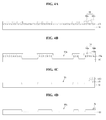
FIGs. 3A to 3D are sectional views illustrating a method of fabricating a light shielding layer, a lower auxiliary electrode, a lower pad electrode, an alignment key, and trenches illustrated inFIG. 1 ; -
FIGs. 4A to 4D are sectional views illustrating a method of fabricating a light shielding layer, a lower auxiliary electrode, a lower pad electrode, an alignment key, and trenches illustrated inFIG. 2 ; -
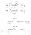
FIG. 5 is a view comparing a comparative example in which no surface treatment is performed on a substrate and an example in which a surface treatment is performed on a substrate with each other; and -
FIGs. 6A to 6H are sectional views illustrating a method of fabricating the organic light-emitting display device ofFIG. 1 . - Hereinafter, embodiments in accordance with the present invention will be described in detail with reference to the accompanying drawings.
-
FIG. 1 is a sectional view illustrating an organic light-emitting display device in accordance with the present invention. - As illustrated in
FIG. 1 , the organic light-emitting display device in accordance with the present invention includes a switching thin-film transistor (not illustrated), a driving thin-film transistor 100, an organic light-emitting diode 130, astorage capacitor 140, anauxiliary electrode 160, asignal pad 150, and analignment key 170. - The driving thin-
film transistor 100 includes agate electrode 106, asource electrode 108, adrain electrode 110, and anoxide semiconductor layer 104. Meanwhile, the switching thin-film transistor has the same configuration as that of the driving thin-film transistor 100, and thus includes the same components as those of the driving thin-film transistor 100. - The
gate electrode 106 is formed on agate insulator pattern 112, which is the same as the pattern of thegate electrode 106. Thegate electrode 106 overlaps theoxide semiconductor layer 104 with thegate insulator pattern 112 interposed therebetween. Thegate electrode 106 may be a single layer or multiple layers formed of any one selected from among molybdenum (Mo), aluminum (Al), chrome (Cr), gold (Au), titanium (Ti), nickel (Ni), neodymium (Nd), and copper (Cu), or an alloy of them, without being limited thereto. - The
source electrode 108 is connected to theoxide semiconductor layer 104 through asource contact hole 124S, which penetrates aninterlayer insulator film 116. Thedrain electrode 110 is connected to theoxide semiconductor layer 104 through adrain contact hole 124D, which penetrates theinterlayer insulator film 116. In addition, thedrain electrode 110 is connected to ananode 132 through apixel contact hole 120, which penetrates aprotective film 118 and aplanarization layer 148. - Each of the
source electrode 108 and thedrain electrode 110 includes a transparentconductive layer 172a and an opaqueconductive layer 172b formed on the transparentconductive layer 172a. The transparentconductive layer 172a may be formed of a transparent conductive material, such as indium tin oxide (ITO), and the opaqueconductive layer 172b may be a single layer or multiple layers formed of any one selected from among molybdenum (Mo), aluminum (Al), chrome (Cr), gold (Au), titanium (Ti), nickel (Ni), neodymium (Nd), and copper (Cu) or an alloy of them, without being limited thereto. - The
oxide semiconductor layer 104 is formed so as to be below thegate insulator pattern 112 and so as to overlap, or extend beyond at least one dimension of, thegate electrode 106, thereby forming a channel between thesource electrode 108 and thedrain electrode 110. Theoxide semiconductor layer 104 is formed of an oxide including at least one metal selected from among Zn, Cd, Ga, In, Sn, Hf and Zr. Afirst buffer layer 126, a heat-resistant buffer layer 122, and asecond buffer layer 128 may be sequentially stacked one above another between theoxide semiconductor layer 104 and alight shielding layer 102 and between asignal link 174 and a lowerauxiliary electrode 162, so as to effectively ensure the stability of the device. Here, the heat-resistant buffer layer 122 and thesecond buffer layer 128 have the same pattern. - The heat-
resistant buffer layer 122 is formed of an organic film material having a lower dielectric constant than those of the first and second buffer layers 126 and 128, for example, acryl resin. The heat-resistant buffer layer 122 is formed below theoxide semiconductor layer 104 of the switching/driving thin-film transistor 100. In addition, the heat-resistant buffer layer 122 is formed belowsignal links 174, each of which connects at least one signal line, selected from among a gate line, a data line, and a power line, with thesignal pad 150. Moreover, the heat-resistant buffer layer 122 is also formed between the signal line and the lowerauxiliary electrode 162, which intersects (overlaps) the signal line. In this way, the parasitic capacitance between the signal line, each signal link, and the lowerauxiliary electrode 162 embedded in atrench 101a of asubstrate 101 and the parasitic capacitance between each electrode of the switching/driving thin-film transistor 100 and thelight shielding layer 102 are reduced in proportion to the dielectric constant of the heat-resistant buffer layer 122. In this way, signal interference between the signal line, each signal link, and the lowerauxiliary electrode 162 embedded in thetrench 101a of thesubstrate 101 and signal interference between each electrode of the switching/driving thin-film transistor 100 and thelight shielding layer 102 may be minimized. - The
second buffer layer 128 is formed on the heat-resistant buffer layer 122 in the same pattern as the heat-resistant buffer layer 122 and serves to prevent the generation of fumes in the heat-resistant buffer layer 122, which is formed of an organic film material. Therefore, thesecond buffer layer 128 may prevent, for example, deterioration of the thin-film transistor 100 due to such fumes. Thesecond buffer layer 128 is formed of SiNx or SiOx, in the same manner as thefirst buffer layer 126. - The
light shielding layer 102, which overlaps theoxide semiconductor layer 104, is embedded in thetrench 101a of thesubstrate 101. Thelight shielding layer 102 may absorb or reflect light introduced from the outside, and therefore may minimize the introduction of light to theoxide semiconductor layer 104. Thelight shielding layer 102 is formed of an opaque metal, such as Mo, Ti, Al, Cu, Cr, Co, W, Ta, Ni, Au, Ag, Sn, and Zn. - The
storage capacitor 140 includes a storagelower electrode 142 and a storageupper electrode 144, which overlap each other with theinterlayer insulator film 116 therebetween. The storagelower electrode 142, which is the same layer as thegate electrode 106, is formed on thegate insulator pattern 112 using the same material as that of thegate electrode 106. The storageupper electrode 144, which is the same layer as thesource electrode 108, is formed on theinterlayer insulator film 116 using the same material as that of thesource electrode 108. - The light-emitting
diode 130 includes theanode 132 connected to thedrain electrode 110 of the thin-film transistor 100, an organic light-emittinglayer 134 formed on theanode 132, and acathode 136 formed over the organic light-emittinglayer 134. - The
anode 132 is connected to thedrain electrode 110, which is exposed through thepixel contact hole 120, which penetrates theprotective film 118 and theplanarization layer 148. Meanwhile, in the case of a top emission type organic light-emitting display device, theanode 132 takes the form of a stack in which a transparent conductive layer, which is formed of, for example, indium tin oxide (ITO) or indium zinc oxide (IZO), and a metal layer, which is formed of, for example, aluminum (Al), silver (Ag), or APC (Ag;Pb;Cu) are stacked one above another. - The organic light-emitting
layer 134 is formed on theanode 132 in a light-emitting area defined by abank 138. The organic light-emittinglayer 134 is formed by stacking, on theanode 132, a hole-related layer, a light-emitting layer, and an electron-related layer, either in that order or in the reverse order. - The
bank 138 has an inner side surface in contact with the organic light-emittinglayer 134, and an outer side surface disposed along the side surface of theanode 132 so as to cover the side surface of theanode 132. As such, because thebank 138 is formed along the rim of theanode 132 except the light-emitting area so as to cover the side surface of theanode 132, the light-emitting area has an island shape. Thebank 138 may be formed of an opaque material (e.g. a black material) in order to prevent optical interference between neighboring sub-pixels. In this case, thebank 138 includes a light shielding formed of at least one selected from among a color pigment, organic black materials and carbon materials. - The
cathode 136 is formed on the upper surface and the side surface of the organic light-emittinglayer 134 and thebank 138 so as to be opposite theanode 132 with the organic light-emittinglayer 134 interposed therebetween. In the case of a top emission type organic light-emitting display device, thecathode 136 is formed of a transparent conductive oxide (TCO). - The
auxiliary electrode 160 is formed in order to reduce the resistance of thecathode 136, which increases as the area of the organic light-emitting display device increases. Theauxiliary electrode 160 includes the lowerauxiliary electrode 162, an intermediateauxiliary electrode 164, and an upperauxiliary electrode 166. - The lower
auxiliary electrode 162 is embedded in thetrench 101a of thesubstrate 101 and is formed of the same material as that of thelight shielding layer 102. Because the lowerauxiliary electrode 162 is embedded in thetrench 101a of thesubstrate 101 so as to be formed below the heat-resistant buffer layer (thick film), which prevents signal interference, unlike a conventional lower auxiliary electrode, which is formed on a thick organic film, process failure, such as erosion, may be prevented, which may ensure structural stability. - The intermediate
auxiliary electrode 164 is electrically connected to the lowerauxiliary electrode 162, which is exposed through a firstauxiliary contact hole 168a, which penetrates thefirst buffer layer 126 and theinterlayer insulator film 116. The intermediateauxiliary electrode 164 includes the transparentconductive layer 172a and the opaqueconductive layer 172b formed on the transparentconductive layer 172a. - The upper
auxiliary electrode 166 is electrically connected to the intermediateauxiliary electrode 164, which is exposed through a secondauxiliary contact hole 168b, which penetrates theprotective film 118 and theplanarization layer 148. The upperauxiliary electrode 166 is formed in the same plane as theanode 132 using the same material as that of theanode 132. - A
partition 146, which is formed on the upperauxiliary electrode 166, has an inversely tapered shape, the width of which gradually increases with decreasing distance to the upper surface of thepartition 146. Through the provision of thepartition 146, the organic light-emittinglayer 134, which is straightly grown, is formed only on the upper surface of thepartition 146 and the upper surface of theanode 132, which is located in the light-emitting area exposed by thebank 138. On the other hand, because thecathode 136, which has step coverage superior to that of the organic light-emittinglayer 134, is also formed on the side surfaces of thepartition 146 and thebank 138, thecathode 136 may be easily brought into contact with the upperauxiliary electrode 166. Meanwhile, although the case where the upperauxiliary electrode 162 is connected to thecathode 136 has been described by way of example, the upperauxiliary electrode 162 may be connected to theanode 132. - The
signal pad 150 is connected to at least one signal line among the gate line, the data line, and the power line through thesignal link 174. Thesignal pad 150 includes alower pad electrode 152 and anupper pad electrode 154. - The
lower pad electrode 152 is formed of the same material as that of thelight shielding layer 102, and is embedded in thetrench 101a of thesubstrate 101. Theupper pad electrode 154 is electrically connected to thelower pad electrode 152, which is exposed through apad contact hole 156, which penetrates thefirst buffer layer 126 and theinterlayer insulator film 116. Theupper pad electrode 154 includes the transparentconductive layer 172a. Theupper pad electrode 154 is exposed outward through apad hole 158, which penetrates the firstprotective film 118. - The
alignment key 170 serves as a rule for positional alignment between thesubstrate 101 and a fabrication device (e.g. a photomask or a shadow mask) that is used to form a thin film on thesubstrate 101. Thealignment key 170 may be embedded in thetrench 101a of thesubstrate 101, in the same manner as thelight shielding layer 102, the lowerauxiliary electrode 162, and thelower pad electrode 152 as illustrated inFIG. 1 , or may be formed on thesubstrate 101 in the state in which each of thelight shielding layer 102, the lowerauxiliary electrode 162, and thelower pad electrode 152 is embedded in thetrench 101a. - The
alignment key 170 illustrated inFIG. 1 is formed via electroplating or electroless plating as illustrated inFIGs. 3A to 3D . Specifically, after aphotoresist pattern 182 is formed on thesubstrate 101 via a photolithography process as illustrated inFIG. 3A , thesubstrate 101 is patterned via an etching process in which thephotoresist pattern 182 is used as a mask, whereby a plurality oftrenches 101a is formed in thesubstrate 101. Subsequently, as illustrated inFIG. 3B , aseed metal 184 is deposited at room temperature on thesubstrate 101 on which thephotoresist pattern 182 remains. Here, theseed metal 184 is a low-resistance metal, such as silver (Ag), gold (Au), copper (Cu), nickel (Ni), tin (Sn), or zinc (Zn). Subsequently, as illustrated inFIG. 3C , thephotoresist pattern 182 and theseed metal 184 on thephotoresist pattern 182 are removed via the stripping of thephotoresist pattern 182. Subsequently, as theseed metal 184 remaining in thetrenches 101a is grown, as illustrated inFIG. 3D , thelight shielding layer 102, the lowerauxiliary electrode 162, thelower pad electrode 152, and thealignment key 170 are simultaneously formed in thetrenches 101a. Meanwhile, thelight shielding layer 102, the lowerauxiliary electrode 162, thelower pad electrode 152, and thealignment key 170, which are formed of the seed metal (e.g. Cu) using electroplating or electroless plating, have the same resistivity as a thin layer, which is formed of copper Cu via deposition. - The
alignment key 170 illustrated inFIG. 2 is formed using amulti-stepped photoresist pattern 186 as illustrated inFIGs. 4A to 4D . Specifically, as illustrated inFIG. 4A , after anopaque metal layer 170a is deposited throughout the surface of thesubstrate 101, themulti-stepped photoresist pattern 186 is formed on theopaque metal layer 170a via a photolithography process using a halftone mask. Themulti-stepped photoresist pattern 186 includes afirst photoresist pattern 186a having a first thickness and asecond photoresist pattern 186b having a second thickness, which is greater than the first thickness. By etching theopaque metal layer 170a and thesubstrate 101 via an etching process in which themulti-stepped photoresist pattern 186 is used as a mask, as illustrated inFIG. 4B , theopaque metal layer 170a remains between themulti-stepped photoresist pattern 186 and thesubstrate 101, and thetrenches 101a are formed in thesubstrate 101. - Subsequently, by ashing the
photoresist pattern 186, thesecond photoresist pattern 186b is reduced in thickness, and thefirst photoresist pattern 186a is removed. By etching theopaque metal layer 170a using thesecond photoresist pattern 186b, having a reduced thickness, as a mask, as illustrated inFIG. 4C , the remainingopaque metal layer 170a excluding theopaque metal layer 170a located below thesecond photoresist pattern 186b is removed. The remainingopaque metal layer 170a below thesecond photoresist pattern 186b becomes thealignment key 170. Thephotoresist pattern 186b remaining on thealignment key 170, as illustrated inFIG. 4D , is removed via a stripping process. After thealignment key 170 is formed, an opaque metal layer is deposited on thesubstrate 101 in which thetrenches 101a have been formed, and thereafter is patterned via a photolithography process and an etching process. Thereby, thelight shielding layer 102, the lowerauxiliary electrode 162, and thelower pad electrode 152 are simultaneously formed in thetrenches 101a. - Meanwhile, an etching process using the
photoresist pattern 182 as a mask is required in order to from thetrenches 101a in thesubstrate 101. However, in the case of a comparative example in which the adhesive force between thesubstrate 101 and thephotoresist pattern 182 is not good, as illustrated inFIG. 5 , an etching solution permeates between thesubstrate 101 and thephotoresist pattern 182. Thereby, an undercut having a first width D1 is formed between the side surface of thesubstrate 101 and thephotoresist pattern 182. The width of thesubstrate 101 located between the neighboringtrenches 101a may be reduced, thus causing short circuits between electrodes embedded in thetrenches 101a and extending the tails of the electrodes in thetrenches 101a, which makes it difficult to achieve high resolution. - On the other hand, in an example of the present invention, prior to applying a photoresist onto the
substrate 101, hexamethyldisilazane (HMDS) is applied onto thesubstrate 101 for the surface treatment of thesubstrate 101. Because HMDS serves to increase adhesive force between thesubstrate 101 and the photoresist, upon etching of thesubstrate 101, it is possible to prevent an etching solution from permeating between thesubstrate 101 and thephotoresist pattern 182. Thereby, an undercut having a second width D2, which is smaller than that of the comparative example, is formed between the side surface of thesubstrate 101 and thephotoresist pattern 182. In this way, the width of thesubstrate 101 located between the neighboringtrenches 101a may be greater than that in the comparative example, thus preventing short circuits between electrodes embedded in thetrenches 101a and shortening the tails of the electrodes in thetrenches 101a, which makes it easy to achieve high resolution. -
FIGs. 6A to 6H are sectional views illustrating a method of fabricating the organic light-emitting display device ofFIG. 1 . Meanwhile, because the method of fabricating the organic light-emitting display device ofFIG. 2 is the same as the method of fabricating the organic light-emitting display device ofFIG. 1 from the formation of thefirst buffer layer 126, a description related to the method of fabricating the organic light-emitting display device ofFIG. 2 is omitted therein. - Referring to
FIG. 6A , as described above with reference toFIGs. 3A to 3D , thetrenches 101a are formed in thesubstrate 101, and thelight shielding layer 102, the lowerauxiliary electrode 162, thelower pad electrode 152, and thealignment key 170 are embedded in thetrenches 101a. - Referring to
FIG. 6B , thefirst buffer layer 126 is formed on thesubstrate 101 in which thelight shielding layer 102, the lowerauxiliary electrode 162, thelower pad electrode 152, and thealignment key 170 have been formed in thetrenches 101a, and the heat-resistant buffer layer 122, thesecond buffer layer 128, and theoxide semiconductor layer 104 are formed on thefirst buffer layer 126. - Specifically, the
first buffer layer 126, the heat-resistant buffer layer 122, thesecond buffer layer 128, and theoxide semiconductor layer 104 are formed via deposition on thesubstrate 101 in which thelight shielding layer 102, the lowerauxiliary electrode 162, thelower pad electrode 152, and thealignment key 170 have been formed in thetrenches 101a. Subsequently, the heat-resistant buffer layer 122, thesecond buffer layer 128, and theoxide semiconductor layer 104 are selectively etched via a photolithography process using a halftone mask and an etching process. Thereby, the heat-resistant buffer layer 122, thesecond buffer layer 128, and theoxide semiconductor layer 104, which have the same pattern, are sequentially stacked one above another in the area at which they overlap thelight shielding layer 102, and the heat-resistant buffer layer 122 and thesecond buffer layer 128 are sequentially stacked one above another in the area at which they overlap the lowerauxiliary electrode 162. - In this way, the heat-
resistant buffer layer 122 and thesecond buffer layer 128 are formed via the same mask process as theoxide semiconductor layer 104. In this case, because the heat-resistant buffer layer 122, which has different etching properties from those of thesecond buffer layer 128 and theoxide semiconductor layer 104, is disposed below thesecond buffer layer 128 and theoxide semiconductor layer 104, process failure, such as the occurrence of undercutting may be prevented after the etching process, and process stability may be acquired. - Referring to
FIG. 6C , thegate insulator pattern 112, thelower storage electrode 142, and thegate electrode 106 are formed on thesubstrate 101 on which the heat-resistant buffer layer 122, thesecond buffer layer 128, and theoxide semiconductor layer 104 have been formed. - Specifically, a gate insulator film is formed on the
substrate 101 on which the heat-resistant buffer layer 122, thesecond buffer layer 128, and theoxide semiconductor layer 104 have been formed, and a gate metal layer is formed on the gate insulator film via deposition, such as sputtering. The gate insulator film is formed of an inorganic insulation material, such as SiOx or SiNx. The gate metal layer may be a single layer formed of a metal, such as Mo, Ti, Cu, AlNd, Al, or Cr, or an alloy thereof, or may be multiple layers using the same. Subsequently, by simultaneously patterning the gate metal layer and the gate insulator film via a photolithography process and an etching process, each of thegate electrode 106 and thelower storage electrode 142 is formed in the same pattern as thegate insulator pattern 112. - Referring to
FIG. 6D , theinterlayer insulator film 116, which has the source and draincontact holes pad contact hole 156, and the firstauxiliary contact hole 168a, is formed on thesubstrate 101 on which thegate electrode 106 and thelower storage electrode 142 are formed. - Specifically, the
interlayer insulator film 116 is formed on thesubstrate 101, on which thegate electrode 106 and thelower storage electrode 142 are formed, via deposition, such as PECVD. Subsequently, by patterning theinterlayer insulator film 116 and thefirst buffer layer 126 via a photolithography process and an etching process, the source and draincontact holes pad contact hole 156, and the firstauxiliary contact hole 168a are formed. - Referring to
FIG. 6E , thesource electrode 108, thedrain electrode 110, theupper storage electrode 144, and theupper pad electrode 154 are formed on theinterlayer insulator film 116, which has the source and draincontact holes pad contact hole 156, and the firstauxiliary contact hole 168a. - Specifically, the transparent
conductive layer 172a and the opaqueconductive layer 174 are sequentially deposited via, for example, sputtering on theinterlayer insulator film 116, which has the source and draincontact holes pad contact hole 156, and the firstauxiliary contact hole 168a. Subsequently, by patterning transparentconductive layer 172a and the opaqueconductive layer 174 via a photolithography process using a halftone mask and an etching process, thesource electrode 108, thedrain electrode 110, theupper storage electrode 144, and theupper pad electrode 154 are formed. At this time, thesource electrode 108, thedrain electrode 110, and theupper storage electrode 144 take the form of a stack including the transparentconductive layer 172a and the opaqueconductive layer 174, and theupper pad electrode 154 is formed of the transparentconductive layer 172a, which has high corrosion resistance and acid resistance. - Referring to
FIG. 6F , theprotective film 118 and theplanarization layer 148, which have thepixel contact hole 120 and the secondauxiliary contact hole 168b, are formed on theinterlayer insulator film 116, on which thesource electrode 108, thedrain electrode 110, theupper storage electrode 144, and theupper pad electrode 154 have been formed. - Specifically, the
protective film 118 and theplanarization layer 148 are sequentially formed on theinterlayer insulator film 116, on which thesource electrode 108, thedrain electrode 110, theupper storage electrode 144, and theupper pad electrode 154 have been formed. Theprotective film 118 is formed of an inorganic insulation material, such as SiOx or SiNx, and theplanarization layer 148 is formed of an organic insulation material, such as photoacryl. Subsequently, by selectively etching theprotective film 118 and theplanarization layer 148 via a photolithography process using a halftone mask and an etching process, thepixel contact hole 120 and the secondauxiliary contact hole 168b are formed. Thepixel contact hole 120 penetrates theprotective film 118 and theplanarization layer 148 so as to expose thedrain electrode 110, and the secondauxiliary contact hole 168b penetrates theprotective film 118 and theplanarization layer 148 so as to expose the intermediateauxiliary electrode 164. Then, theplanarization layer 148 is selectively removed from the top of thesignal pad 150 so that theprotective film 118 on the top of thesignal pad 150 is exposed. - Referring to
FIG. 6G , theanode 132, thebank 138, and thepad hole 158 are formed on thesubstrate 101 on which theprotective film 118 and theplanarization layer 148, which have thepixel contact hole 120 and the secondauxiliary contact hole 168b, have been formed. - Specifically, an opaque conductive film and a bank photosensitive film are applied throughout the surface of the
substrate 101 on which theprotective film 118 has been formed. Subsequently, by patterning the bank photosensitive film, the opaque conductive film, and theprotective film 118 via a photolithography process using a halftone mask and an etching process, theanode 132, thebank 138, and thepad hole 158 are formed. - Referring to
FIG. 6H , thepartition 146, the organic light-emittinglayer 134, and thecathode 136 are sequentially formed on thesubstrate 101, which has theanode 132, thebank 138, and thepad hole 158. - Specifically, after a partition photosensitive film is applied onto the substrate having the
anode 132, thebank 138, and thepad hole 158, the partition photosensitive film is patterned via a photolithography process so as to form the inversely taperedpartition 146. Subsequently, the organic light-emittinglayer 134 is formed in the light-emitting area exposed by thebank 138, and thecathode 136 is formed on thesubstrate 101 on which the organic light-emittinglayer 134 has been formed. - As described above, in the organic light-emitting display device in accordance with the present invention, the
light shielding layer 102 and the lowerauxiliary electrode 162 are formed via the same single mask process, and theoxide semiconductor layer 104, the heat-resistant buffer layer 122, and thesecond buffer layer 128 are formed via the same single mask process. In this way, the organic light-emitting display device in accordance with the present invention may reduce the number of mask processes by a total of at least 2 processes compared to the prior art, thereby achieving enhanced productivity and reduced costs. - In addition, in the present invention, because the lower
auxiliary electrode 162 is embedded in thetrench 101a of thesubstrate 101 and the heat-resistant buffer layer 122 is disposed on thesubstrate 101, the heat-resistant buffer layer may prevent corrosion failure of a signal line including the lowerauxiliary electrode 162, thereby ensuring structural stability. - Meanwhile, although the present invention has described the case where the
semiconductor layer 104 of the driving thin-film transistor 100 is formed of an oxide by way of example, thesemiconductor layer 104 of the driving thin-film transistor 100 may be formed of polysilicon. - It will be apparent to those skilled in the art that the present invention described above is not limited to the embodiments described above and the accompanying drawings, and various substitutions, modifications, and alterations may be devised within the scope of the present invention, which is defined by the appended claims.
- The following is a list of aspects of the present invention.
- Aspect 1. An organic light-emitting display device comprising:
- a substrate having a plurality of trenches;
- a thin film transistor disposed on the substrate;
- a light-emitting diode connected to the thin film transistor;
- an upper auxiliary electrode connected to any one of an anode and a cathode of the light-emitting diode; and
- a lower auxiliary electrode embedded in the trench and connected to the upper auxiliary electrode.
- Aspect 2. The device according to aspect 1, further comprising:
- a light shielding layer located in an area overlapping the thin-film transistor and embedded in the trench; and
- a first buffer layer, a heat-resistant buffer layer, and a second buffer layer sequentially stacked one above another between the light shielding layer and the thin film transistor.
- Aspect 3. The device according to aspect 2, wherein the heat-resistant buffer layer is composed of an organic film material having a lower dielectric constant than those of the first and second buffer layers.
- Aspect 4. The device according to aspect 3, further comprising:
- a signal link located above the lower auxiliary electrode; and
- a signal pad connected to the signal link,
- wherein the first buffer layer, the heat-resistant buffer layer, and the second buffer layer are sequentially stacked one above another between the lower auxiliary electrode and the signal link, and
- wherein the signal pad includes:
- a lower pad electrode embedded in the trench; and
- an upper pad electrode connected to the lower pad electrode exposed through a pad contact hole, the pad contact hole penetrating the first buffer layer and an interlayer insulator film.
- Aspect 5. The device according to aspect 4, further comprising an alignment key embedded in the trench, or disposed on the substrate.
- Aspect 6. A method of fabricating an organic light-emitting display device, the method comprising:
- providing a substrate having a plurality of trenches in which a lower auxiliary electrode is embedded;
- forming a thin film transistor on the substrate in which the lower auxiliary electrode has been formed;
- forming an anode connected to the thin film transistor and an upper auxiliary electrode connected to the lower auxiliary electrode;
- forming an organic light-emitting layer on the anode; and
- forming a cathode on the organic light-emitting layer.
-
Aspect 7. The method according to aspect 6, wherein the providing includes:- forming a photoresist pattern on the substrate;
- forming the trenches by etching the substrate using the photoresist pattern;
- depositing a seed metal throughout a surface of the substrate on which the photoresist pattern remains;
- removing the photoresist pattern and the seed metal on the photoresist pattern; and
- forming the lower auxiliary electrode and an alignment key embedded in the trenches by growing the seed metal.
- Aspect 8. The method according to aspect 6, wherein the providing includes:
- Forming, on the substrate, an opaque metal layer and a multi-stepped photoresist pattern on the opaque metal layer;
- forming the trenches by etching the substrate and the opaque metal layer using the multi-stepped photoresist pattern;
- ashing the multi-stepped photoresist pattern;
- forming an alignment key by etching the opaque metal layer using the ashed photoresist pattern; and
- forming the lower auxiliary electrode embedded in the trench, formed in the substrate in which the alignment key has been formed.
- Aspect 9. The method according to
aspect 7, further comprising:- forming a light shielding layer, which is disposed in an area overlapping the thin film transistor and is embedded in the trench, simultaneously with formation of the lower auxiliary electrode;
- forming a first buffer layer on the substrate in which the light shielding layer, the lower auxiliary electrode, and the alignment key have been formed;
- forming, on the first buffer layer, a heat-resistant buffer layer, a second buffer layer, and a semiconductor layer of the thin film transistor, which overlap the light shielding layer, and simultaneously forming the heat-resistant buffer layer and the second buffer layer, which overlap the lower auxiliary electrode;
- forming a gate insulator pattern and a gate electrode of the thin film transistor on the semiconductor layer of the thin film transistor;
- forming an interlayer insulator film on the gate electrode of the thin film transistor; and
- forming source and drain electrodes of the thin film transistor and a signal link on the interlayer insulator film.
- Aspect 10. The method according to aspect 8, further comprising:
- forming a light shielding layer, which is disposed in an area overlapping the thin film transistor and is embedded in the trench, simultaneously with formation of the lower auxiliary electrode;
- forming a first buffer layer on the substrate in which the light shielding layer, the lower auxiliary electrode, and the alignment key have been formed;
- forming, on the first buffer layer, a heat-resistant buffer layer, a second buffer layer, and a semiconductor layer of the thin film transistor, which overlap the light shielding layer, and simultaneously forming the heat-resistant buffer layer and the second buffer layer, which overlap the lower auxiliary electrode;
- forming a gate insulator pattern and a gate electrode of the thin film transistor on the semiconductor layer of the thin film transistor;
- forming an interlayer insulator film on the gate electrode of the thin film transistor; and
- forming source and drain electrodes of the thin film transistor and a signal link on the interlayer insulator film.
Claims (15)
- An organic light-emitting display device comprising:a substrate (101) having a plurality of trenches (101a);a thin film transistor (100) disposed on the substrate (101) ;a light-emitting diode (130) connected to the thin film transistor (100);an upper auxiliary electrode (166) connected to any one of an anode (132) and a cathode (136) of the light-emitting diode (130); and
a lower auxiliary electrode (162) embedded in an auxiliary electrode trench of the substrate and connected to the upper auxiliary electrode (166). - The organic light-emitting display device of claim 1, further comprising a first buffer layer (126) formed on the substrate (101).
- The organic light-emitting display device of claim 2, further comprising a light shielding layer (102) overlapping with the thin-film transistor (100), wherein the light shielding layer (102) is embedded in a light shielding trench of the substrate (101).
- The organic light-emitting display device of claim 3, further comprising:a heat-resistant buffer layer (122), anda second buffer layer (128);wherein the first buffer layer (126), the heat-resistant buffer layer (122), and the second buffer layer (128) are sequentially stacked one above another between the light shielding layer (102) and the thin film transistor (100).
- The organic light-emitting display device of claim 4, wherein the heat-resistant buffer layer (122) is composed of an organic film material having a lower dielectric constant than those of the first (126) and second buffer layers (128).
- The organic light-emitting display device of any one of the preceding claims that is dependent on claim 2, further comprising a lower pad electrode (152) embedded in a lower pad trench of the substrate (101) and an upper pad electrode (154) connected to the lower pad electrode (152) through the first buffer layer (126).
- The organic light-emitting display device of claim 6, further comprising:a signal link (174) located above the lower auxiliary electrode (162); anda signal pad (150) connected to the signal link,wherein the first buffer layer (126), the heat-resistant buffer layer (122), and the second buffer layer (128) are sequentially stacked one above another between the lower auxiliary electrode (162) and the signal link (174), andwherein:the signal pad (150) includes the lower pad electrode (152) and the upper pad electrode (154);the upper pad electrode (154) is connected to the lower pad electrode (152) through a pad contact hole (156), andthe pad contact hole (156) being located the first buffer layer (126) and an interlayer insulator film (116).
- The organic light-emitting display device of claims 1 to 7, further comprising an alignment key (170) embedded in an alignment key trench of the substrate (101), or disposed on the substrate (101).
- A method of fabricating an organic light-emitting display device, the method comprising:Providing a substrate (101) having a plurality of trenches (101a) in which a lower auxiliary electrode is embedded (162);forming a thin film transistor (100) on the substrate (101) in which the lower auxiliary electrode (162) has been formed;forming an anode (132) connected to the thin film transistor (100) and an upper auxiliary electrode (166) connected to the lower auxiliary electrode (162);forming an organic light-emitting layer (134) on the anode; andforming a cathode (136) on the organic light-emitting layer (134).
- The method according to claim 9, wherein the providing includes:forming a photoresist pattern (182) on the substrate (101) ;forming the trenches by etching the substrate (101) using the photoresist pattern (182);depositing a seed metal (184) throughout a surface of the substrate (101) on which the photoresist pattern (182) remains;removing the photoresist pattern (182 and the seed metal on the photoresist pattern; andforming the lower auxiliary electrode (162) and an alignment key (170), which are embedded in the trenches, by growing the seed metal.
- The method according to claim 9, wherein the providing includes:forming, on the substrate, an opaque metal layer and a multi-stepped photoresist pattern (186) on the opaque metal layer (170a);forming the trenches (101a) by etching the substrate and the opaque metal layer (170a) using the multi-stepped photoresist pattern (186);ashing the multi-stepped photoresist pattern (186);forming an alignment key (170) by etching the opaque metal layer (170a) using the ashed photoresist pattern; andforming the lower auxiliary electrode (162) in the trench formed in the substrate in which the alignment key (170) has been formed.
- The method according to claim 10, further comprising:simultaneously forming a light shielding layer (102), in an area overlapping the thin film transistor (100), and the lower auxiliary electrode (162) in respective trenches in the substrate (101);forming a first buffer layer (126) on the substrate (101) in which the light shielding layer (102), the lower auxiliary electrode (162), and the alignment key (170) have been formed;forming, on the first buffer layer (126), a heat-resistant buffer layer (122), a second buffer layer (128), and a semiconductor layer (104) of the thin film transistor (101) which overlap the light shielding layer (102), and simultaneously forming the heat-resistant buffer layer (122) and the second buffer layer (128), which overlap the lower auxiliary electrode (160);forming a gate insulator pattern (112) and a gate electrode (106) of the thin film transistor (100) on the semiconductor layer (104) of the thin film transistor (100);forming an interlayer insulator film (116) on the gate electrode (106) of the thin film transistor (100); andforming source (108) and drain (110) electrodes of the thin film transistor (100) and a signal link (174) on the interlayer insulator film (116).
- The method according to claim 11, further comprising:simultaneously forming a light shielding layer (102), in an area overlapping the thin film transistor (100), and the lower auxiliary electrode (162) in respective trenches of the substrate;forming a first buffer layer (126) on the substrate (101) in which the light shielding layer (102), the lower auxiliary electrode (162), and the alignment key (170) have been formed;forming, on the first buffer layer (126), a heat-resistant buffer layer (122), a second buffer layer (128), and a semiconductor layer (104) of the thin film transistor (100), which overlap the light shielding layer (102), and simultaneously forming the heat-resistant buffer layer (122) and the second buffer layer (128), which overlap the lower auxiliary electrode (162);forming a gate insulator pattern (112) and a gate electrode (106) of the thin film transistor (100) on the semiconductor layer (104) of the thin film transistor (100);forming an interlayer insulator film (116) on the gate electrode (106) of the thin film transistor (100); andforming source (108) and drain (110) electrodes of the thin film transistor (100) and a signal link (174) on the interlayer insulator film (116).
- The method of fabricating an organic light-emitting display device of claim 9, further comprising forming a buffer layer on the provided substrate (101).
- The method of fabricating an organic light-emitting display device of claim 9, wherein the provided substrate (101) has a lower pad electrode (152) embedded, and the method further includes connecting an upper pad electrode (154) to the lower pad electrode (152) through the buffer layer.
Applications Claiming Priority (1)
| Application Number | Priority Date | Filing Date | Title |
|---|---|---|---|
| KR1020150188439A KR102458907B1 (en) | 2015-12-29 | 2015-12-29 | Organic light emitting display and method of fabricating the same |
Publications (2)
| Publication Number | Publication Date |
|---|---|
| EP3188274A1 true EP3188274A1 (en) | 2017-07-05 |
| EP3188274B1 EP3188274B1 (en) | 2019-04-03 |
Family
ID=56893821
Family Applications (1)
| Application Number | Title | Priority Date | Filing Date |
|---|---|---|---|
| EP16187892.1A Active EP3188274B1 (en) | 2015-12-29 | 2016-09-08 | Organic light-emitting display device and method of fabricating the same |
Country Status (5)
| Country | Link |
|---|---|
| US (2) | US10050098B2 (en) |
| EP (1) | EP3188274B1 (en) |
| JP (1) | JP6348166B2 (en) |
| KR (1) | KR102458907B1 (en) |
| CN (1) | CN107039491B (en) |
Cited By (3)
| Publication number | Priority date | Publication date | Assignee | Title |
|---|---|---|---|---|
| EP3843154A1 (en) * | 2019-12-24 | 2021-06-30 | InnoLux Corporation | Display device |
| EP3846220A1 (en) * | 2019-12-31 | 2021-07-07 | LG Display Co., Ltd. | Display panel and method of manufacturing same |
| US11968863B2 (en) | 2018-08-29 | 2024-04-23 | Semiconductor Energy Laboratory Co., Ltd. | Display panel, display device, input/output device, and data processing device |
Families Citing this family (95)
| Publication number | Priority date | Publication date | Assignee | Title |
|---|---|---|---|---|
| KR102405695B1 (en) | 2015-08-31 | 2022-06-03 | 엘지디스플레이 주식회사 | Organic light emitting display device and method of manufacturing the same |
| CA3002752A1 (en) | 2015-10-26 | 2017-05-04 | Oti Lumionics Inc. | Method for patterning a coating on a surface and device including a patterned coating |
| KR102443645B1 (en) * | 2016-01-13 | 2022-09-15 | 삼성디스플레이 주식회사 | Organic light emitting diode display and manufacturing method thereof |
| KR102424445B1 (en) * | 2016-05-03 | 2022-07-22 | 삼성디스플레이 주식회사 | Thin film transistor array panel and manufacturing method thereof |
| KR102627284B1 (en) * | 2016-05-12 | 2024-01-22 | 엘지디스플레이 주식회사 | Method of manufacturing a connection structure connecting cathode electrode to auxiliary cathode electrode, and organic light emitting diode display device using the same |
| US10020351B2 (en) * | 2016-06-24 | 2018-07-10 | Lg Display Co., Ltd. | Electroluminescence display device |
| KR102873476B1 (en) * | 2016-07-29 | 2025-10-20 | 엘지디스플레이 주식회사 | Organic Light Emitting Display Device |
| KR102854033B1 (en) * | 2016-11-30 | 2025-09-02 | 엘지디스플레이 주식회사 | Organic light emitting diode display device |
| KR102802931B1 (en) | 2016-12-02 | 2025-05-08 | 오티아이 루미오닉스 인크. | Device including a conductive coating disposed over emissive regions and method therefor |
| KR102773737B1 (en) * | 2016-12-14 | 2025-02-27 | 엘지디스플레이 주식회사 | Organic light emitting display |
| KR102563713B1 (en) | 2017-04-26 | 2023-08-07 | 오티아이 루미오닉스 인크. | Methods of patterning the coating of a surface and apparatus comprising the patterned coating |
| US10295875B2 (en) * | 2017-05-12 | 2019-05-21 | A.U. Vista, Inc. | TFT array having conducting lines with low resistance |
| CN110832660B (en) | 2017-05-17 | 2023-07-28 | Oti照明公司 | Method of selectively depositing a conductive coating on a patterned coating and an apparatus comprising the conductive coating |
| CN108933154B (en) * | 2017-05-26 | 2021-04-27 | 京东方科技集团股份有限公司 | Preparation method of organic light emitting diode display substrate, display substrate and display device |
| CN109103215B (en) * | 2017-06-21 | 2021-03-09 | 京东方科技集团股份有限公司 | Organic light emitting diode display panel, manufacturing method thereof and display device |
| CN107464836B (en) * | 2017-07-19 | 2020-04-10 | 深圳市华星光电半导体显示技术有限公司 | Manufacturing method of top gate type thin film transistor and top gate type thin film transistor |
| TWI653747B (en) * | 2017-07-25 | 2019-03-11 | 友達光電股份有限公司 | Array substrate and method of manufacturing same |
| CN107565048B (en) * | 2017-08-24 | 2020-05-26 | 京东方科技集团股份有限公司 | Method for preparing an array substrate, array substrate and display device |
| CN107565049B (en) * | 2017-08-25 | 2019-11-01 | 京东方科技集团股份有限公司 | AMOLED display panel and preparation method thereof |
| CN109757118B (en) * | 2017-09-04 | 2021-09-03 | 京东方科技集团股份有限公司 | Display substrate and display device |
| CN109509768B (en) * | 2017-09-15 | 2024-06-04 | 京东方科技集团股份有限公司 | Display panel, manufacturing method thereof and display device |
| US10756292B2 (en) * | 2017-10-13 | 2020-08-25 | Shenzhen China Star Optoelectronics Semiconductor Display Technology Co., Ltd. | Method of manufacturing an OLED panel and an OLED panel |
| KR102461391B1 (en) | 2017-10-16 | 2022-10-31 | 엘지디스플레이 주식회사 | Large Area Organic Light Emitting Diode Display |
| CN107845739B (en) * | 2017-11-07 | 2023-10-17 | 深圳市华星光电半导体显示技术有限公司 | An OLED device, OLED display panel and preparation method |
| CN108010943B (en) * | 2017-11-28 | 2019-04-02 | 深圳市华星光电半导体显示技术有限公司 | OLED display panel and its manufacturing method |
| KR102014179B1 (en) * | 2017-12-08 | 2019-08-26 | 엘지디스플레이 주식회사 | Organic light emitting display device and method for manufacturing the same |
| KR102489043B1 (en) | 2017-12-27 | 2023-01-16 | 엘지디스플레이 주식회사 | Organic light emitting display device |
| KR102506035B1 (en) * | 2017-12-27 | 2023-03-03 | 엘지디스플레이 주식회사 | Electroluminescent display device |
| KR102457997B1 (en) * | 2017-12-29 | 2022-10-21 | 엘지디스플레이 주식회사 | Electroluminescent Display Device |
| US11751415B2 (en) | 2018-02-02 | 2023-09-05 | Oti Lumionics Inc. | Materials for forming a nucleation-inhibiting coating and devices incorporating same |
| US11489136B2 (en) | 2018-05-07 | 2022-11-01 | Oti Lumionics Inc. | Method for providing an auxiliary electrode and device including an auxiliary electrode |
| KR102569929B1 (en) * | 2018-07-02 | 2023-08-24 | 삼성디스플레이 주식회사 | Display apparatus |
| CN109065751A (en) | 2018-07-25 | 2018-12-21 | 武汉华星光电技术有限公司 | Display module and electronic device |
| KR102654918B1 (en) * | 2018-10-08 | 2024-04-05 | 삼성디스플레이 주식회사 | Display apparatus |
| CN109638038B (en) * | 2018-11-15 | 2021-04-02 | 武汉华星光电半导体显示技术有限公司 | An active array organic light emitting diode display module |
| CN109285874A (en) * | 2018-11-23 | 2019-01-29 | 京东方科技集团股份有限公司 | Array substrate, method for making the same, and display device |
| JP2022508040A (en) | 2018-11-23 | 2022-01-19 | オーティーアイ ルミオニクス インコーポレーテッド | Optoelectronic device containing light transmission region |
| KR102607781B1 (en) * | 2018-12-28 | 2023-11-28 | 엘지디스플레이 주식회사 | Electroluminance Lighting Device Having High Aperture Ratio |
| JP6791283B2 (en) * | 2019-02-15 | 2020-11-25 | セイコーエプソン株式会社 | Electro-optics, electronic devices, and methods of manufacturing electro-optics |
| KR20250160226A (en) | 2019-03-07 | 2025-11-11 | 오티아이 루미오닉스 인크. | Materials for forming a nucleation-inhibiting coating and devices incorporating same |
| WO2020210943A1 (en) * | 2019-04-15 | 2020-10-22 | Boe Technology Group Co., Ltd. | Display substrate, display apparatus, method of fabricating display substrate |
| JP7555600B2 (en) | 2019-04-18 | 2024-09-25 | オーティーアイ ルミオニクス インコーポレーテッド | Materials for forming nucleation-inhibiting coatings and devices incorporating same - Patents.com |
| US11049884B2 (en) | 2019-04-28 | 2021-06-29 | Wuhan China Star Optoelectronics Semiconductor Display Technology Co., Ltd. | Display panel and method of manufacturing same, and display module |
| CN110148599B (en) * | 2019-04-28 | 2023-06-30 | 武汉华星光电半导体显示技术有限公司 | Display panel and manufacturing method thereof |
| JP7576337B2 (en) | 2019-05-08 | 2024-11-01 | オーティーアイ ルミオニクス インコーポレーテッド | Materials for forming nucleation-inhibiting coatings and devices incorporating same - Patents.com |
| KR102814725B1 (en) * | 2019-05-13 | 2025-05-30 | 삼성디스플레이 주식회사 | Display apparatus |
| CN110335886A (en) * | 2019-06-21 | 2019-10-15 | 武汉华星光电半导体显示技术有限公司 | Array substrate |
| US11832473B2 (en) | 2019-06-26 | 2023-11-28 | Oti Lumionics Inc. | Optoelectronic device including light transmissive regions, with light diffraction characteristics |
| KR20240134240A (en) | 2019-06-26 | 2024-09-06 | 오티아이 루미오닉스 인크. | Optoelectronic device including light transmissive regions with light diffraction characteristics |
| CN110265460A (en) * | 2019-06-27 | 2019-09-20 | 京东方科技集团股份有限公司 | OLED display substrate, manufacturing method thereof, and display device |
| KR102720609B1 (en) * | 2019-07-19 | 2024-10-24 | 삼성디스플레이 주식회사 | Flexible display device |
| KR20210016145A (en) * | 2019-07-31 | 2021-02-15 | 삼성디스플레이 주식회사 | Display device and method of manufacturing the same |
| KR102818817B1 (en) | 2019-08-09 | 2025-06-11 | 오티아이 루미오닉스 인크. | Optoelectronic device including auxiliary electrode and partition |
| JP7352826B2 (en) * | 2019-10-21 | 2023-09-29 | セイコーエプソン株式会社 | Electro-optical devices and electronic equipment |
| CN115605999B (en) * | 2019-10-29 | 2026-04-03 | 京东方科技集团股份有限公司 | A display substrate, its manufacturing method, and a display device. |
| WO2021120207A1 (en) * | 2019-12-20 | 2021-06-24 | 京东方科技集团股份有限公司 | Display device, display panel, and fabrication method therefor |
| CN113035902A (en) | 2019-12-24 | 2021-06-25 | 群创光电股份有限公司 | Display device |
| CN115552643B (en) | 2019-12-24 | 2025-08-19 | Oti照明公司 | Light emitting device including cover layer and method of manufacturing the same |
| KR102777206B1 (en) * | 2019-12-24 | 2025-03-05 | 엘지디스플레이 주식회사 | Thin film trnasistor, and display panel and display apparatus using the same |
| KR102918336B1 (en) * | 2019-12-27 | 2026-01-27 | 엘지디스플레이 주식회사 | Display panel and display device including the same |
| KR102687966B1 (en) * | 2019-12-30 | 2024-07-23 | 엘지디스플레이 주식회사 | Display device |
| CN111244114B (en) * | 2020-02-10 | 2023-10-17 | Tcl华星光电技术有限公司 | display panel |
| CN111312732B (en) * | 2020-03-04 | 2024-04-12 | 深圳市华星光电半导体显示技术有限公司 | Display panel, manufacturing method thereof, display module and electronic device |
| CN111628105B (en) * | 2020-06-04 | 2023-05-26 | 京东方科技集团股份有限公司 | Display panel and manufacturing method thereof, display substrate and manufacturing method thereof, and display device |
| US11197384B1 (en) * | 2020-06-29 | 2021-12-07 | Quanta Computer Inc. | Tool-less latch system for a node sled |
| KR102853564B1 (en) * | 2020-07-10 | 2025-09-02 | 삼성디스플레이 주식회사 | Display device and method of fabricating the same |
| CN111883574A (en) * | 2020-09-02 | 2020-11-03 | 深圳市华星光电半导体显示技术有限公司 | OLED display panel and manufacturing method thereof |
| CN112002833A (en) * | 2020-09-24 | 2020-11-27 | 京东方科技集团股份有限公司 | Method of manufacturing organic light emitting display panel, and display device |
| KR102875343B1 (en) * | 2020-10-14 | 2025-10-22 | 엘지디스플레이 주식회사 | Display apparatus |
| KR20220064456A (en) * | 2020-11-11 | 2022-05-19 | 삼성디스플레이 주식회사 | Display device and manufacturing method thereof |
| JP7570896B2 (en) * | 2020-11-17 | 2024-10-22 | 株式会社ジャパンディスプレイ | Display device |
| JP7520697B2 (en) * | 2020-11-17 | 2024-07-23 | 株式会社ジャパンディスプレイ | Display device |
| KR20220080801A (en) * | 2020-12-07 | 2022-06-15 | 삼성디스플레이 주식회사 | Display apparatus and manufacturing the same |
| US11985841B2 (en) | 2020-12-07 | 2024-05-14 | Oti Lumionics Inc. | Patterning a conductive deposited layer using a nucleation inhibiting coating and an underlying metallic coating |
| KR102913093B1 (en) * | 2020-12-09 | 2026-01-14 | 엘지디스플레이 주식회사 | Electroluminescence display device |
| KR102838108B1 (en) * | 2020-12-31 | 2025-07-23 | 엘지디스플레이 주식회사 | Electroluminescent Display Device |
| WO2022175784A1 (en) * | 2021-02-19 | 2022-08-25 | 株式会社半導体エネルギー研究所 | Display device |
| WO2022198573A1 (en) | 2021-03-25 | 2022-09-29 | 京东方科技集团股份有限公司 | Display substrate and display device |
| GB2610080A (en) | 2021-03-25 | 2023-02-22 | Boe Technology Group Co Ltd | Display substrate and display apparatus |
| CN115606333A (en) | 2021-04-21 | 2023-01-13 | 京东方科技集团股份有限公司(Cn) | Display substrate, manufacturing method thereof, and display device |
| KR102851145B1 (en) * | 2021-07-26 | 2025-08-28 | 삼성디스플레이 주식회사 | Display apparatus |
| KR20230023841A (en) | 2021-08-10 | 2023-02-20 | 삼성디스플레이 주식회사 | Display device and method for manufacturing of the same |
| WO2023019530A1 (en) * | 2021-08-19 | 2023-02-23 | 京东方科技集团股份有限公司 | Display apparatus, and display panel and manufacturing method therefor |
| CN113871432B (en) * | 2021-09-17 | 2023-05-05 | 深圳市华星光电半导体显示技术有限公司 | Display panel |
| KR102828905B1 (en) * | 2021-10-01 | 2025-07-04 | 엘지디스플레이 주식회사 | Thin film transistor array substrate and display device |
| CN114023764A (en) * | 2021-10-20 | 2022-02-08 | 武汉华星光电半导体显示技术有限公司 | Display panel and display device |
| CN114141852B (en) * | 2021-11-30 | 2023-05-05 | 深圳市华星光电半导体显示技术有限公司 | Flexible display panel and flexible display device |
| KR20230105756A (en) * | 2022-01-04 | 2023-07-12 | 삼성디스플레이 주식회사 | Display device |
| CN114530458B (en) * | 2022-01-27 | 2022-11-29 | 长沙惠科光电有限公司 | Display panel and method for manufacturing display panel |
| KR20230120151A (en) * | 2022-02-07 | 2023-08-17 | 삼성디스플레이 주식회사 | Display device and manufacturing method of the same |
| CN114784065A (en) * | 2022-04-11 | 2022-07-22 | 深圳市华星光电半导体显示技术有限公司 | Display panel, display device and manufacturing method of display panel |
| CN114975550A (en) * | 2022-05-24 | 2022-08-30 | 深圳市华星光电半导体显示技术有限公司 | Display panel, manufacturing method and electronic equipment |
| CN115295581A (en) * | 2022-06-07 | 2022-11-04 | 深圳市华星光电半导体显示技术有限公司 | Display panel and display device |
| KR20240022055A (en) * | 2022-08-10 | 2024-02-20 | 삼성디스플레이 주식회사 | Display apparatus and manufacturing method thereof |
| JP2024128372A (en) * | 2023-03-10 | 2024-09-24 | 株式会社ジャパンディスプレイ | Display device motherboard and display device |
Citations (4)
| Publication number | Priority date | Publication date | Assignee | Title |
|---|---|---|---|---|
| JPH1140368A (en) * | 1997-07-17 | 1999-02-12 | Nec Corp | Organic el element |
| JP2002015866A (en) * | 2000-06-30 | 2002-01-18 | Seiko Epson Corp | Manufacturing method of organic EL display |
| US20100156860A1 (en) * | 2008-12-22 | 2010-06-24 | Sony Corporation | Display apparatus and electronic apparatus |
| US20120146030A1 (en) * | 2010-12-14 | 2012-06-14 | Samsung Mobile Display Co., Ltd. | Organic Light-Emitting Display Device and Method of Manufacturing the Same |
Family Cites Families (13)
| Publication number | Priority date | Publication date | Assignee | Title |
|---|---|---|---|---|
| TW364275B (en) | 1996-03-12 | 1999-07-11 | Idemitsu Kosan Co | Organic electroluminescent element and organic electroluminescent display device |
| US6524877B1 (en) | 1999-10-26 | 2003-02-25 | Semiconductor Energy Laboratory Co., Ltd. | Semiconductor device, and method of fabricating the same |
| JP3968519B2 (en) * | 2002-12-03 | 2007-08-29 | ソニー株式会社 | Manufacturing method of display device |
| JP2007150258A (en) | 2005-10-27 | 2007-06-14 | Seiko Epson Corp | Pattern forming method, film structure, electro-optical device, and electronic apparatus |
| JP4896671B2 (en) | 2006-11-06 | 2012-03-14 | 三菱電機株式会社 | Halftone mask and pattern substrate manufacturing method using the same |
| KR100788545B1 (en) * | 2006-12-29 | 2007-12-26 | 삼성에스디아이 주식회사 | Organic electroluminescent display and manufacturing method thereof |
| KR101418588B1 (en) | 2007-11-14 | 2014-07-16 | 삼성디스플레이 주식회사 | Display substrate and manufacturing method thereof |
| JP2009271188A (en) * | 2008-05-01 | 2009-11-19 | Seiko Epson Corp | Organic electro-luminescence device and manufacturing method therefor |
| KR101912406B1 (en) * | 2012-04-12 | 2019-01-07 | 삼성디스플레이 주식회사 | Backplane for flat panel display apparatus, the method of manufacturing for the backplane, and organic light emitting display apparatus comprising the backplane |
| KR101922177B1 (en) * | 2012-04-17 | 2019-02-14 | 삼성디스플레이 주식회사 | Organic light emitting display apparatus and method of manufacturing organic light emitting display apparatus |
| CN102981335A (en) * | 2012-11-15 | 2013-03-20 | 京东方科技集团股份有限公司 | Pixel unit structure, array substrate and display device |
| KR102206412B1 (en) * | 2012-12-27 | 2021-01-22 | 엘지디스플레이 주식회사 | Thin film transistor, method for manufacturing the same and display device comprising the same |
| KR20170038964A (en) * | 2015-09-30 | 2017-04-10 | 삼성디스플레이 주식회사 | Display Panel and method of manufacturing the same |
-
2015
- 2015-12-29 KR KR1020150188439A patent/KR102458907B1/en active Active
-
2016
- 2016-09-08 EP EP16187892.1A patent/EP3188274B1/en active Active
- 2016-10-21 US US15/299,690 patent/US10050098B2/en active Active
- 2016-11-24 CN CN201611052889.3A patent/CN107039491B/en active Active
- 2016-12-27 JP JP2016252990A patent/JP6348166B2/en active Active
-
2018
- 2018-07-23 US US16/043,125 patent/US10504985B2/en active Active
Patent Citations (4)
| Publication number | Priority date | Publication date | Assignee | Title |
|---|---|---|---|---|
| JPH1140368A (en) * | 1997-07-17 | 1999-02-12 | Nec Corp | Organic el element |
| JP2002015866A (en) * | 2000-06-30 | 2002-01-18 | Seiko Epson Corp | Manufacturing method of organic EL display |
| US20100156860A1 (en) * | 2008-12-22 | 2010-06-24 | Sony Corporation | Display apparatus and electronic apparatus |
| US20120146030A1 (en) * | 2010-12-14 | 2012-06-14 | Samsung Mobile Display Co., Ltd. | Organic Light-Emitting Display Device and Method of Manufacturing the Same |
Cited By (7)
| Publication number | Priority date | Publication date | Assignee | Title |
|---|---|---|---|---|
| US11968863B2 (en) | 2018-08-29 | 2024-04-23 | Semiconductor Energy Laboratory Co., Ltd. | Display panel, display device, input/output device, and data processing device |
| US12436634B2 (en) | 2018-08-29 | 2025-10-07 | Semiconductor Energy Laboratory Co., Ltd. | Display panel, display device, input/output device, and data processing device |
| EP3843154A1 (en) * | 2019-12-24 | 2021-06-30 | InnoLux Corporation | Display device |
| US11626460B2 (en) | 2019-12-24 | 2023-04-11 | Innolux Corporation | Display device including blue organic light emitting diode and blue light blocking layer |
| EP3846220A1 (en) * | 2019-12-31 | 2021-07-07 | LG Display Co., Ltd. | Display panel and method of manufacturing same |
| TWI755977B (en) * | 2019-12-31 | 2022-02-21 | 南韓商Lg顯示器股份有限公司 | Display panel and method of manufacturing same |
| US12022676B2 (en) | 2019-12-31 | 2024-06-25 | Lg Display Co., Ltd. | Display panel having cathode electrode in contact with connection electrode in shade region and method of manufacturing same |
Also Published As
| Publication number | Publication date |
|---|---|
| JP6348166B2 (en) | 2018-06-27 |
| EP3188274B1 (en) | 2019-04-03 |
| CN107039491B (en) | 2020-10-09 |
| KR20170078175A (en) | 2017-07-07 |
| US10050098B2 (en) | 2018-08-14 |
| US20180331169A1 (en) | 2018-11-15 |
| CN107039491A (en) | 2017-08-11 |
| US20170186831A1 (en) | 2017-06-29 |
| US10504985B2 (en) | 2019-12-10 |
| KR102458907B1 (en) | 2022-10-25 |
| JP2017120782A (en) | 2017-07-06 |
Similar Documents
| Publication | Publication Date | Title |
|---|---|---|
| EP3188274B1 (en) | Organic light-emitting display device and method of fabricating the same | |
| CN108022948B (en) | Organic light emitting display device and method of manufacturing the same | |
| US10672339B2 (en) | Organic light-emitting display device | |
| US10367046B2 (en) | Organic light-emitting display device and method of manufacturing the same | |
| US9653520B2 (en) | Organic light emitting display panel and method of manufacturing the same | |
| US10403696B2 (en) | Organic light emitting display device and method of fabricating the same | |
| KR101622645B1 (en) | Method of Manufacturing of the Organic Light Emitting Display Device | |
| US20180138251A1 (en) | Organic light-emitting display device and manufacturing method thereof | |
| KR20110015240A (en) | Organic light emitting display device and manufacturing method | |
| CN115811897A (en) | Display panel and electronic device | |
| KR20180013227A (en) | Organic light emitting display and fabricating method thereof | |
| KR101330376B1 (en) | Oxide Thin Film Transistor and Method for fabricating Organic Light Emitting Display Device using the same | |
| KR102119572B1 (en) | Thin film transistor array substrate and method for fabricating the same | |
| KR102693149B1 (en) | Substrate for display and display including the same | |
| KR20170079632A (en) | Organic light emitting display device and method for fabricating the same | |
| KR20130051214A (en) | Thin film transistor substrate and method of manufacturing the same | |
| KR20160121090A (en) | Organic light emitting display device and method of manufacturing the same |
Legal Events
| Date | Code | Title | Description |
|---|---|---|---|
| PUAI | Public reference made under article 153(3) epc to a published international application that has entered the european phase |
Free format text: ORIGINAL CODE: 0009012 |
|
| STAA | Information on the status of an ep patent application or granted ep patent |
Free format text: STATUS: THE APPLICATION HAS BEEN PUBLISHED |
|
| AK | Designated contracting states |
Kind code of ref document: A1 Designated state(s): AL AT BE BG CH CY CZ DE DK EE ES FI FR GB GR HR HU IE IS IT LI LT LU LV MC MK MT NL NO PL PT RO RS SE SI SK SM TR |
|
| AX | Request for extension of the european patent |
Extension state: BA ME |
|
| STAA | Information on the status of an ep patent application or granted ep patent |
Free format text: STATUS: REQUEST FOR EXAMINATION WAS MADE |
|
| 17P | Request for examination filed |
Effective date: 20180104 |
|
| RBV | Designated contracting states (corrected) |
Designated state(s): AL AT BE BG CH CY CZ DE DK EE ES FI FR GB GR HR HU IE IS IT LI LT LU LV MC MK MT NL NO PL PT RO RS SE SI SK SM TR |
|
| STAA | Information on the status of an ep patent application or granted ep patent |
Free format text: STATUS: EXAMINATION IS IN PROGRESS |
|
| 17Q | First examination report despatched |
Effective date: 20180404 |
|
| GRAP | Despatch of communication of intention to grant a patent |
Free format text: ORIGINAL CODE: EPIDOSNIGR1 |
|
| STAA | Information on the status of an ep patent application or granted ep patent |
Free format text: STATUS: GRANT OF PATENT IS INTENDED |
|
| INTG | Intention to grant announced |
Effective date: 20181009 |
|
| GRAS | Grant fee paid |
Free format text: ORIGINAL CODE: EPIDOSNIGR3 |
|
| GRAA | (expected) grant |
Free format text: ORIGINAL CODE: 0009210 |
|
| STAA | Information on the status of an ep patent application or granted ep patent |
Free format text: STATUS: THE PATENT HAS BEEN GRANTED |
|
| AK | Designated contracting states |
Kind code of ref document: B1 Designated state(s): AL AT BE BG CH CY CZ DE DK EE ES FI FR GB GR HR HU IE IS IT LI LT LU LV MC MK MT NL NO PL PT RO RS SE SI SK SM TR |
|
| REG | Reference to a national code |
Ref country code: GB Ref legal event code: FG4D |
|
| REG | Reference to a national code |
Ref country code: AT Ref legal event code: REF Ref document number: 1116826 Country of ref document: AT Kind code of ref document: T Effective date: 20190415 Ref country code: CH Ref legal event code: EP |
|
| REG | Reference to a national code |
Ref country code: DE Ref legal event code: R096 Ref document number: 602016011798 Country of ref document: DE |
|
| REG | Reference to a national code |
Ref country code: IE Ref legal event code: FG4D |
|
| REG | Reference to a national code |
Ref country code: NL Ref legal event code: FP |
|
| REG | Reference to a national code |
Ref country code: LT Ref legal event code: MG4D |
|
| REG | Reference to a national code |
Ref country code: AT Ref legal event code: MK05 Ref document number: 1116826 Country of ref document: AT Kind code of ref document: T Effective date: 20190403 |
|
| PG25 | Lapsed in a contracting state [announced via postgrant information from national office to epo] |
Ref country code: AL Free format text: LAPSE BECAUSE OF FAILURE TO SUBMIT A TRANSLATION OF THE DESCRIPTION OR TO PAY THE FEE WITHIN THE PRESCRIBED TIME-LIMIT Effective date: 20190403 Ref country code: SE Free format text: LAPSE BECAUSE OF FAILURE TO SUBMIT A TRANSLATION OF THE DESCRIPTION OR TO PAY THE FEE WITHIN THE PRESCRIBED TIME-LIMIT Effective date: 20190403 Ref country code: PT Free format text: LAPSE BECAUSE OF FAILURE TO SUBMIT A TRANSLATION OF THE DESCRIPTION OR TO PAY THE FEE WITHIN THE PRESCRIBED TIME-LIMIT Effective date: 20190803 Ref country code: ES Free format text: LAPSE BECAUSE OF FAILURE TO SUBMIT A TRANSLATION OF THE DESCRIPTION OR TO PAY THE FEE WITHIN THE PRESCRIBED TIME-LIMIT Effective date: 20190403 Ref country code: HR Free format text: LAPSE BECAUSE OF FAILURE TO SUBMIT A TRANSLATION OF THE DESCRIPTION OR TO PAY THE FEE WITHIN THE PRESCRIBED TIME-LIMIT Effective date: 20190403 Ref country code: LT Free format text: LAPSE BECAUSE OF FAILURE TO SUBMIT A TRANSLATION OF THE DESCRIPTION OR TO PAY THE FEE WITHIN THE PRESCRIBED TIME-LIMIT Effective date: 20190403 Ref country code: FI Free format text: LAPSE BECAUSE OF FAILURE TO SUBMIT A TRANSLATION OF THE DESCRIPTION OR TO PAY THE FEE WITHIN THE PRESCRIBED TIME-LIMIT Effective date: 20190403 Ref country code: CZ Free format text: LAPSE BECAUSE OF FAILURE TO SUBMIT A TRANSLATION OF THE DESCRIPTION OR TO PAY THE FEE WITHIN THE PRESCRIBED TIME-LIMIT Effective date: 20190403 Ref country code: NO Free format text: LAPSE BECAUSE OF FAILURE TO SUBMIT A TRANSLATION OF THE DESCRIPTION OR TO PAY THE FEE WITHIN THE PRESCRIBED TIME-LIMIT Effective date: 20190703 |
|
| PG25 | Lapsed in a contracting state [announced via postgrant information from national office to epo] |
Ref country code: GR Free format text: LAPSE BECAUSE OF FAILURE TO SUBMIT A TRANSLATION OF THE DESCRIPTION OR TO PAY THE FEE WITHIN THE PRESCRIBED TIME-LIMIT Effective date: 20190704 Ref country code: PL Free format text: LAPSE BECAUSE OF FAILURE TO SUBMIT A TRANSLATION OF THE DESCRIPTION OR TO PAY THE FEE WITHIN THE PRESCRIBED TIME-LIMIT Effective date: 20190403 Ref country code: RS Free format text: LAPSE BECAUSE OF FAILURE TO SUBMIT A TRANSLATION OF THE DESCRIPTION OR TO PAY THE FEE WITHIN THE PRESCRIBED TIME-LIMIT Effective date: 20190403 Ref country code: LV Free format text: LAPSE BECAUSE OF FAILURE TO SUBMIT A TRANSLATION OF THE DESCRIPTION OR TO PAY THE FEE WITHIN THE PRESCRIBED TIME-LIMIT Effective date: 20190403 Ref country code: BG Free format text: LAPSE BECAUSE OF FAILURE TO SUBMIT A TRANSLATION OF THE DESCRIPTION OR TO PAY THE FEE WITHIN THE PRESCRIBED TIME-LIMIT Effective date: 20190703 |
|
| PG25 | Lapsed in a contracting state [announced via postgrant information from national office to epo] |
Ref country code: AT Free format text: LAPSE BECAUSE OF FAILURE TO SUBMIT A TRANSLATION OF THE DESCRIPTION OR TO PAY THE FEE WITHIN THE PRESCRIBED TIME-LIMIT Effective date: 20190403 Ref country code: IS Free format text: LAPSE BECAUSE OF FAILURE TO SUBMIT A TRANSLATION OF THE DESCRIPTION OR TO PAY THE FEE WITHIN THE PRESCRIBED TIME-LIMIT Effective date: 20190803 |
|
| REG | Reference to a national code |
Ref country code: DE Ref legal event code: R097 Ref document number: 602016011798 Country of ref document: DE |
|
| PG25 | Lapsed in a contracting state [announced via postgrant information from national office to epo] |
Ref country code: RO Free format text: LAPSE BECAUSE OF FAILURE TO SUBMIT A TRANSLATION OF THE DESCRIPTION OR TO PAY THE FEE WITHIN THE PRESCRIBED TIME-LIMIT Effective date: 20190403 Ref country code: EE Free format text: LAPSE BECAUSE OF FAILURE TO SUBMIT A TRANSLATION OF THE DESCRIPTION OR TO PAY THE FEE WITHIN THE PRESCRIBED TIME-LIMIT Effective date: 20190403 Ref country code: DK Free format text: LAPSE BECAUSE OF FAILURE TO SUBMIT A TRANSLATION OF THE DESCRIPTION OR TO PAY THE FEE WITHIN THE PRESCRIBED TIME-LIMIT Effective date: 20190403 Ref country code: SK Free format text: LAPSE BECAUSE OF FAILURE TO SUBMIT A TRANSLATION OF THE DESCRIPTION OR TO PAY THE FEE WITHIN THE PRESCRIBED TIME-LIMIT Effective date: 20190403 |
|
| PLBE | No opposition filed within time limit |
Free format text: ORIGINAL CODE: 0009261 |
|
| STAA | Information on the status of an ep patent application or granted ep patent |
Free format text: STATUS: NO OPPOSITION FILED WITHIN TIME LIMIT |
|
| PG25 | Lapsed in a contracting state [announced via postgrant information from national office to epo] |
Ref country code: SM Free format text: LAPSE BECAUSE OF FAILURE TO SUBMIT A TRANSLATION OF THE DESCRIPTION OR TO PAY THE FEE WITHIN THE PRESCRIBED TIME-LIMIT Effective date: 20190403 Ref country code: IT Free format text: LAPSE BECAUSE OF FAILURE TO SUBMIT A TRANSLATION OF THE DESCRIPTION OR TO PAY THE FEE WITHIN THE PRESCRIBED TIME-LIMIT Effective date: 20190403 |
|
| 26N | No opposition filed |
Effective date: 20200106 |
|
| PG25 | Lapsed in a contracting state [announced via postgrant information from national office to epo] |
Ref country code: TR Free format text: LAPSE BECAUSE OF FAILURE TO SUBMIT A TRANSLATION OF THE DESCRIPTION OR TO PAY THE FEE WITHIN THE PRESCRIBED TIME-LIMIT Effective date: 20190403 |
|
| PG25 | Lapsed in a contracting state [announced via postgrant information from national office to epo] |
Ref country code: MC Free format text: LAPSE BECAUSE OF FAILURE TO SUBMIT A TRANSLATION OF THE DESCRIPTION OR TO PAY THE FEE WITHIN THE PRESCRIBED TIME-LIMIT Effective date: 20190403 Ref country code: SI Free format text: LAPSE BECAUSE OF FAILURE TO SUBMIT A TRANSLATION OF THE DESCRIPTION OR TO PAY THE FEE WITHIN THE PRESCRIBED TIME-LIMIT Effective date: 20190403 |
|
| REG | Reference to a national code |
Ref country code: CH Ref legal event code: PL |
|
| PG25 | Lapsed in a contracting state [announced via postgrant information from national office to epo] |
Ref country code: CH Free format text: LAPSE BECAUSE OF NON-PAYMENT OF DUE FEES Effective date: 20190930 Ref country code: IE Free format text: LAPSE BECAUSE OF NON-PAYMENT OF DUE FEES Effective date: 20190908 Ref country code: LU Free format text: LAPSE BECAUSE OF NON-PAYMENT OF DUE FEES Effective date: 20190908 Ref country code: LI Free format text: LAPSE BECAUSE OF NON-PAYMENT OF DUE FEES Effective date: 20190930 |
|
| REG | Reference to a national code |
Ref country code: BE Ref legal event code: MM Effective date: 20190930 |
|
| PG25 | Lapsed in a contracting state [announced via postgrant information from national office to epo] |
Ref country code: BE Free format text: LAPSE BECAUSE OF NON-PAYMENT OF DUE FEES Effective date: 20190930 |
|
| PG25 | Lapsed in a contracting state [announced via postgrant information from national office to epo] |
Ref country code: CY Free format text: LAPSE BECAUSE OF FAILURE TO SUBMIT A TRANSLATION OF THE DESCRIPTION OR TO PAY THE FEE WITHIN THE PRESCRIBED TIME-LIMIT Effective date: 20190403 |
|
| PG25 | Lapsed in a contracting state [announced via postgrant information from national office to epo] |
Ref country code: HU Free format text: LAPSE BECAUSE OF FAILURE TO SUBMIT A TRANSLATION OF THE DESCRIPTION OR TO PAY THE FEE WITHIN THE PRESCRIBED TIME-LIMIT; INVALID AB INITIO Effective date: 20160908 Ref country code: MT Free format text: LAPSE BECAUSE OF FAILURE TO SUBMIT A TRANSLATION OF THE DESCRIPTION OR TO PAY THE FEE WITHIN THE PRESCRIBED TIME-LIMIT Effective date: 20190403 |
|
| PG25 | Lapsed in a contracting state [announced via postgrant information from national office to epo] |
Ref country code: MK Free format text: LAPSE BECAUSE OF FAILURE TO SUBMIT A TRANSLATION OF THE DESCRIPTION OR TO PAY THE FEE WITHIN THE PRESCRIBED TIME-LIMIT Effective date: 20190403 |
|
| REG | Reference to a national code |
Ref country code: DE Ref legal event code: R079 Ref document number: 602016011798 Country of ref document: DE Free format text: PREVIOUS MAIN CLASS: H01L0051520000 Ipc: H10K0050800000 |
|
| PGFP | Annual fee paid to national office [announced via postgrant information from national office to epo] |
Ref country code: NL Payment date: 20250722 Year of fee payment: 10 |
|
| PGFP | Annual fee paid to national office [announced via postgrant information from national office to epo] |
Ref country code: DE Payment date: 20250721 Year of fee payment: 10 |
|
| PGFP | Annual fee paid to national office [announced via postgrant information from national office to epo] |
Ref country code: GB Payment date: 20250722 Year of fee payment: 10 |
|
| PGFP | Annual fee paid to national office [announced via postgrant information from national office to epo] |
Ref country code: FR Payment date: 20250725 Year of fee payment: 10 |