EP3188246A1 - Metal gate transistor and fabrication method thereof - Google Patents
Metal gate transistor and fabrication method thereof Download PDFInfo
- Publication number
- EP3188246A1 EP3188246A1 EP16205794.7A EP16205794A EP3188246A1 EP 3188246 A1 EP3188246 A1 EP 3188246A1 EP 16205794 A EP16205794 A EP 16205794A EP 3188246 A1 EP3188246 A1 EP 3188246A1
- Authority
- EP
- European Patent Office
- Prior art keywords
- dielectric layer
- layer
- etch stop
- metal gate
- dummy gate
- Prior art date
- Legal status (The legal status is an assumption and is not a legal conclusion. Google has not performed a legal analysis and makes no representation as to the accuracy of the status listed.)
- Withdrawn
Links
Images




Classifications
-
- H—ELECTRICITY
- H10—SEMICONDUCTOR DEVICES; ELECTRIC SOLID-STATE DEVICES NOT OTHERWISE PROVIDED FOR
- H10D—INORGANIC ELECTRIC SEMICONDUCTOR DEVICES
- H10D30/00—Field-effect transistors [FET]
- H10D30/01—Manufacture or treatment
- H10D30/021—Manufacture or treatment of FETs having insulated gates [IGFET]
- H10D30/027—Manufacture or treatment of FETs having insulated gates [IGFET] of lateral single-gate IGFETs
-
- H—ELECTRICITY
- H10—SEMICONDUCTOR DEVICES; ELECTRIC SOLID-STATE DEVICES NOT OTHERWISE PROVIDED FOR
- H10W—GENERIC PACKAGES, INTERCONNECTIONS, CONNECTORS OR OTHER CONSTRUCTIONAL DETAILS OF DEVICES COVERED BY CLASS H10
- H10W20/00—Interconnections in chips, wafers or substrates
- H10W20/20—Interconnections within wafers or substrates, e.g. through-silicon vias [TSV]
-
- H—ELECTRICITY
- H10—SEMICONDUCTOR DEVICES; ELECTRIC SOLID-STATE DEVICES NOT OTHERWISE PROVIDED FOR
- H10D—INORGANIC ELECTRIC SEMICONDUCTOR DEVICES
- H10D30/00—Field-effect transistors [FET]
- H10D30/01—Manufacture or treatment
- H10D30/021—Manufacture or treatment of FETs having insulated gates [IGFET]
- H10D30/024—Manufacture or treatment of FETs having insulated gates [IGFET] of fin field-effect transistors [FinFET]
-
- H—ELECTRICITY
- H10—SEMICONDUCTOR DEVICES; ELECTRIC SOLID-STATE DEVICES NOT OTHERWISE PROVIDED FOR
- H10D—INORGANIC ELECTRIC SEMICONDUCTOR DEVICES
- H10D64/00—Electrodes of devices having potential barriers
- H10D64/01—Manufacture or treatment
- H10D64/015—Manufacture or treatment removing at least parts of gate spacers, e.g. disposable spacers
-
- H—ELECTRICITY
- H10—SEMICONDUCTOR DEVICES; ELECTRIC SOLID-STATE DEVICES NOT OTHERWISE PROVIDED FOR
- H10D—INORGANIC ELECTRIC SEMICONDUCTOR DEVICES
- H10D64/00—Electrodes of devices having potential barriers
- H10D64/01—Manufacture or treatment
- H10D64/017—Manufacture or treatment using dummy gates in processes wherein at least parts of the final gates are self-aligned to the dummy gates, i.e. replacement gate processes
-
- H—ELECTRICITY
- H10—SEMICONDUCTOR DEVICES; ELECTRIC SOLID-STATE DEVICES NOT OTHERWISE PROVIDED FOR
- H10D—INORGANIC ELECTRIC SEMICONDUCTOR DEVICES
- H10D64/00—Electrodes of devices having potential barriers
- H10D64/60—Electrodes characterised by their materials
- H10D64/66—Electrodes having a conductor capacitively coupled to a semiconductor by an insulator, e.g. MIS electrodes
- H10D64/665—Electrodes having a conductor capacitively coupled to a semiconductor by an insulator, e.g. MIS electrodes the conductor comprising a layer of elemental metal contacting the insulator, e.g. tungsten or molybdenum
-
- H—ELECTRICITY
- H10—SEMICONDUCTOR DEVICES; ELECTRIC SOLID-STATE DEVICES NOT OTHERWISE PROVIDED FOR
- H10D—INORGANIC ELECTRIC SEMICONDUCTOR DEVICES
- H10D64/00—Electrodes of devices having potential barriers
- H10D64/60—Electrodes characterised by their materials
- H10D64/66—Electrodes having a conductor capacitively coupled to a semiconductor by an insulator, e.g. MIS electrodes
- H10D64/667—Electrodes having a conductor capacitively coupled to a semiconductor by an insulator, e.g. MIS electrodes the conductor comprising a layer of alloy material, compound material or organic material contacting the insulator, e.g. TiN workfunction layers
-
- H—ELECTRICITY
- H10—SEMICONDUCTOR DEVICES; ELECTRIC SOLID-STATE DEVICES NOT OTHERWISE PROVIDED FOR
- H10P—GENERIC PROCESSES OR APPARATUS FOR THE MANUFACTURE OR TREATMENT OF DEVICES COVERED BY CLASS H10
- H10P14/00—Formation of materials, e.g. in the shape of layers or pillars
- H10P14/60—Formation of materials, e.g. in the shape of layers or pillars of insulating materials
- H10P14/63—Formation of materials, e.g. in the shape of layers or pillars of insulating materials characterised by the formation processes
- H10P14/6326—Deposition processes
- H10P14/6328—Deposition from the gas or vapour phase
- H10P14/6334—Deposition from the gas or vapour phase using decomposition or reaction of gaseous or vapour phase compounds, i.e. chemical vapour deposition
-
- H—ELECTRICITY
- H10—SEMICONDUCTOR DEVICES; ELECTRIC SOLID-STATE DEVICES NOT OTHERWISE PROVIDED FOR
- H10P—GENERIC PROCESSES OR APPARATUS FOR THE MANUFACTURE OR TREATMENT OF DEVICES COVERED BY CLASS H10
- H10P14/00—Formation of materials, e.g. in the shape of layers or pillars
- H10P14/60—Formation of materials, e.g. in the shape of layers or pillars of insulating materials
- H10P14/63—Formation of materials, e.g. in the shape of layers or pillars of insulating materials characterised by the formation processes
- H10P14/6326—Deposition processes
- H10P14/6328—Deposition from the gas or vapour phase
- H10P14/6334—Deposition from the gas or vapour phase using decomposition or reaction of gaseous or vapour phase compounds, i.e. chemical vapour deposition
- H10P14/6339—Deposition from the gas or vapour phase using decomposition or reaction of gaseous or vapour phase compounds, i.e. chemical vapour deposition deposition by cyclic CVD, e.g. ALD, ALE or pulsed CVD
-
- H—ELECTRICITY
- H10—SEMICONDUCTOR DEVICES; ELECTRIC SOLID-STATE DEVICES NOT OTHERWISE PROVIDED FOR
- H10P—GENERIC PROCESSES OR APPARATUS FOR THE MANUFACTURE OR TREATMENT OF DEVICES COVERED BY CLASS H10
- H10P14/00—Formation of materials, e.g. in the shape of layers or pillars
- H10P14/60—Formation of materials, e.g. in the shape of layers or pillars of insulating materials
- H10P14/69—Inorganic materials
- H10P14/692—Inorganic materials composed of oxides, glassy oxides or oxide-based glasses
- H10P14/6921—Inorganic materials composed of oxides, glassy oxides or oxide-based glasses containing silicon
- H10P14/6922—Inorganic materials composed of oxides, glassy oxides or oxide-based glasses containing silicon the material containing Si, O and at least one of H, N, C, F or other non-metal elements, e.g. SiOC, SiOC:H or SiONC
- H10P14/6927—Inorganic materials composed of oxides, glassy oxides or oxide-based glasses containing silicon the material containing Si, O and at least one of H, N, C, F or other non-metal elements, e.g. SiOC, SiOC:H or SiONC the material being a silicon oxynitride, e.g. SiON or SiON:H
-
- H—ELECTRICITY
- H10—SEMICONDUCTOR DEVICES; ELECTRIC SOLID-STATE DEVICES NOT OTHERWISE PROVIDED FOR
- H10P—GENERIC PROCESSES OR APPARATUS FOR THE MANUFACTURE OR TREATMENT OF DEVICES COVERED BY CLASS H10
- H10P14/00—Formation of materials, e.g. in the shape of layers or pillars
- H10P14/60—Formation of materials, e.g. in the shape of layers or pillars of insulating materials
- H10P14/69—Inorganic materials
- H10P14/694—Inorganic materials composed of nitrides
- H10P14/6943—Inorganic materials composed of nitrides containing silicon
- H10P14/69433—Inorganic materials composed of nitrides containing silicon the material being a silicon nitride not containing oxygen, e.g. SixNy or SixByNz
-
- H—ELECTRICITY
- H10—SEMICONDUCTOR DEVICES; ELECTRIC SOLID-STATE DEVICES NOT OTHERWISE PROVIDED FOR
- H10W—GENERIC PACKAGES, INTERCONNECTIONS, CONNECTORS OR OTHER CONSTRUCTIONAL DETAILS OF DEVICES COVERED BY CLASS H10
- H10W20/00—Interconnections in chips, wafers or substrates
- H10W20/01—Manufacture or treatment
- H10W20/031—Manufacture or treatment of conductive parts of the interconnections
- H10W20/032—Manufacture or treatment of conductive parts of the interconnections of conductive barrier, adhesion or liner layers
- H10W20/033—Manufacture or treatment of conductive parts of the interconnections of conductive barrier, adhesion or liner layers in openings in dielectrics
-
- H—ELECTRICITY
- H10—SEMICONDUCTOR DEVICES; ELECTRIC SOLID-STATE DEVICES NOT OTHERWISE PROVIDED FOR
- H10W—GENERIC PACKAGES, INTERCONNECTIONS, CONNECTORS OR OTHER CONSTRUCTIONAL DETAILS OF DEVICES COVERED BY CLASS H10
- H10W20/00—Interconnections in chips, wafers or substrates
- H10W20/01—Manufacture or treatment
- H10W20/031—Manufacture or treatment of conductive parts of the interconnections
- H10W20/069—Manufacture or treatment of conductive parts of the interconnections by forming self-aligned vias or self-aligned contact plugs
-
- H—ELECTRICITY
- H10—SEMICONDUCTOR DEVICES; ELECTRIC SOLID-STATE DEVICES NOT OTHERWISE PROVIDED FOR
- H10W—GENERIC PACKAGES, INTERCONNECTIONS, CONNECTORS OR OTHER CONSTRUCTIONAL DETAILS OF DEVICES COVERED BY CLASS H10
- H10W20/00—Interconnections in chips, wafers or substrates
- H10W20/01—Manufacture or treatment
- H10W20/071—Manufacture or treatment of dielectric parts thereof
- H10W20/074—Manufacture or treatment of dielectric parts thereof of dielectric parts comprising thin functional dielectric layers, e.g. dielectric etch-stop, barrier, capping or liner layers
- H10W20/076—Manufacture or treatment of dielectric parts thereof of dielectric parts comprising thin functional dielectric layers, e.g. dielectric etch-stop, barrier, capping or liner layers in via holes or trenches
-
- H—ELECTRICITY
- H10—SEMICONDUCTOR DEVICES; ELECTRIC SOLID-STATE DEVICES NOT OTHERWISE PROVIDED FOR
- H10W—GENERIC PACKAGES, INTERCONNECTIONS, CONNECTORS OR OTHER CONSTRUCTIONAL DETAILS OF DEVICES COVERED BY CLASS H10
- H10W20/00—Interconnections in chips, wafers or substrates
- H10W20/01—Manufacture or treatment
- H10W20/071—Manufacture or treatment of dielectric parts thereof
- H10W20/074—Manufacture or treatment of dielectric parts thereof of dielectric parts comprising thin functional dielectric layers, e.g. dielectric etch-stop, barrier, capping or liner layers
- H10W20/077—Manufacture or treatment of dielectric parts thereof of dielectric parts comprising thin functional dielectric layers, e.g. dielectric etch-stop, barrier, capping or liner layers on sidewalls or on top surfaces of conductors
Definitions
- the present invention generally relates to the field of semiconductor fabrication technology and, more particularly, relates to a metal gate transistor and fabrication methods thereof.
- MOSFET metal-oxide-semiconductor field-effect transistor
- the current technology uses high-k (dielectric constant or permittivity) dielectric material to replace the traditional SiO 2 dielectric material.
- the current technology also uses metal gate to match with the high-k dielectric material.
- a number of factors such as the size of the via and the overlay (OVL) offset in aligning the photomask and the substrate, may cause a short circuit between the metal gate and the formed contact plug in the source/drain region, which may reduce device yield.
- the size of the via and the OVL offset in aligning the photomask and the substrate may be reduced in order to improve device yield, but process cost may also be increased.
- the disclosed fabrication method and metal gate transistor are directed to solve one or more problems set forth above and other problems in the art.
- a first aspect of the present invention includes a method for fabricating a metal gate transistor.
- the method includes forming a dummy gate structure and a first dielectric layer on a semiconductor substrate and a source/drain region in the semiconductor substrate on each side of the dummy gate structure.
- the dummy gate structure is surrounded by the first dielectric layer and the top surface of the dummy gate structure is leveled with the top surface of the first dielectric layer.
- the method then includes forming an etch stop sidewall in the first dielectric layer on each side of the dummy gate structure.
- the top surface of the etch stop sidewall is leveled with the top surfaces of the first dielectric layer and the dummy gate structure.
- the method further includes forming a first trench by removing the dummy gate structure, and forming a metal gate structure to partially fill the first trench.
- the top portion of the first trench becomes a second trench.
- the method also includes forming an etch stop layer by filling the second trench, and forming a contact plug in the first dielectric layer to electrically connect to each source/drain region.
- Forming the etch stop sidewall in the first dielectric layer on each side of the dummy gate structure may further include: removing a top portion of the first dielectric layer to expose a portion of the dummy gate structure; forming a sidewall on each side surface of the exposed portion of the dummy gate structure; depositing a material of the first dielectric layer to cover the dummy gate structure, the sidewalls, and a remaining portion of the first dielectric layer; and forming the etch stop sidewall on each side of the dummy gate structure by removing a top portion of the corresponding sidewall.
- Forming the metal gate structure to partially fill the first trench may further include: sequentially filling a high-k dielectric layer, a work function layer, and a metal gate into the first trench; and removing a top portion of the high-k dielectric layer, the work function layer, and the metal gate.
- Forming the contact plug to electrically connect to each source/drain region may further include: forming a patterned mask layer on the top surfaces of the first dielectric layer, the etch stop layer, and the etch stop sidewalls, wherein an opening is formed in the patterned mask layer corresponding to each source/drain region; forming a via in the semiconductor substrate corresponding to each source/drain region by etching the first dielectric layer, the etch stop layer, and the etch stop sidewalls using the patterned mask layer as an etch mask; and forming the contact plug to electrically connect to each source/drain region by filling the corresponding via with a conductive material.
- a second dielectric layer may be formed on the top surfaces of the etch stop layer, the first dielectric layer, and the etch stop sidewalls, and coordinately. Then, the patterned mask layer may be formed on the top surface of the second dielectric layer. Further, the vias may be formed in the first dielectric layer and the second dielectric layer by etching the second dielectric layer, the first dielectric layer, the etch stop layer, and the etch stop sidewalls using the patterned mask layer as an etch mask.
- the first dielectric layer is separated from the dummy gate structure and the semiconductor substrate by contact-via etch stop layers.
- an offset spacer is formed on each side of the dummy gate structure.
- the dummy gate structure includes a dummy gate insulating layer formed on the semiconductor substrate and a dummy gate electrode formed on the top of the dummy gate insulating layer.
- the dummy gate structure may further include a dummy gate structure hard mask layer formed on the dummy gate electrode.
- the etch stop sidewalls may be made of at least one of SiN x , SiON, SiOBN, SiOCN.
- the etch stop sidewalls are formed by an atomic layer deposition or a chemical vapor deposition method.
- the etch stop layer may be made of at least one of SiN x , SiON, SiOBN, SiOCN.
- the etch stop layer is formed by an atomic layer deposition or a chemical vapor deposition method.
- the metal gate transistor is a planar FET or a fin-FET.
- a second aspect of the present invention provides an alternative method for fabricating the metal gate transistor.
- the method includes forming a high-k dielectric layer on a semiconductor substrate and a dummy gate electrode on the high-k dielectric layer.
- the method also includes forming a source/drain region in the semiconductor substrate on each side of the high-k dielectric layer and a first dielectric layer on the semiconductor substrate to surround the high-k dielectric layer and the dummy gate electrode.
- the top surface of the dummy gate electrode is leveled with the top surface of the first dielectric layer.
- the method includes forming an etch stop sidewall in the first dielectric layer on each side of the dummy gate electrode.
- the top surface of the etch stop sidewall is leveled with the top surfaces of the first dielectric layer and the dummy gate electrode.
- the method includes forming a first trench by removing the dummy gate electrode, and forming a metal gate structure to partially fill the first trench.
- the high-k dielectric layer is the dielectric layer of the formed metal gate structure and a top portion of the first trench becomes a second trench.
- the method also includes forming an etch stop layer to fill the second trench, and forming a contact plug in the first dielectric layer to electrically connect to each source/drain region.
- Forming the etch stop sidewall in the first dielectric layer on each side of the dummy gate electrode may further include: removing a top portion of the first dielectric layer to expose a portion of the dummy gate electrode; forming a sidewall on each side surface of the exposed portion of the dummy gate electrode; depositing a material of the first dielectric layer to cover the dummy gate electrode, the sidewalls, and a remaining portion of the first dielectric layer; and forming the etch stop sidewall on each side of the dummy gate electrode by removing a top portion of the corresponding sidewall.
- Forming the metal gate structure to partially fill the first trench may further include: sequentially filling a work function layer and a metal gate into the first trench; and removing a top portion of the work function layer and the metal gate.
- Forming the contact plug to electrically connect to each source/drain region may further include: forming a patterned mask layer on the top surfaces of the first dielectric layer, the etch stop layer, and the etch stop sidewalls, wherein an opening is formed in the patterned mask layer corresponding to each source/drain region; forming a via in the semiconductor substrate corresponding to each source/drain region by etching the first dielectric layer, the etch stop layer, and the etch stop sidewalls using the patterned mask layer as an etch mask; and forming the contact plug to electrically connect to each source/drain region by filling the corresponding via with a conductive material.
- a second dielectric layer may be formed on the top surfaces of the etch stop layer, the first dielectric layer, and the etch stop sidewalls, and coordinately. Then, the patterned mask layer may be formed on the top surface of the second dielectric layer. Further, the vias may be formed in the first dielectric layer and the second dielectric layer by etching the second dielectric layer, the first dielectric layer, the etch stop layer, and the etch stop sidewalls using the patterned mask layer as an etch mask.
- the high-k dielectric layer may be made of at least one of La 2 O 3 , BaZrO 3 , HfZrO, HfZrON, HfLaO, HfSiO, HfSiON, LaSiO, AlSiO, HfTaO, HfTiO, BaO, TiO, Ti2O 3 , TiO 2 , SrO, Al 2 O 3 , Si 3 N 4 .
- the work function layer may be made of at least one of Ti, Al, Ti x Al 1-x , TiC, TiAlC.
- the metal gate may be made of W.
- a dry etching process is performed to remove the top portion of the high-k dielectric layer, the work function layer, and the metal gate, an etching gas containing at least one of CF 4 , CHF 3 , and C 3 F 8 , together with SF 6 , or contains at least one of CF 4 , CHF 3 , and C 3 F 8 , together with Cl 2 is used.
- a HF acid solution is used as an etching solution while when a wet etching process is performed to remove the top portion of the work function layer and the metal gate, a mixture of NH 4 OH, H 2 O 2 , and water, or a mixture of HCl, H 2 O 2 , and water is used as a wet etching solution.
- a third aspect of the present invention provides a metal gate transistor.
- the metal gate transistor includes a semiconductor substrate, a metal gate structure including a high-k dielectric layer formed on the semiconductor substrate, a work function layer formed on the high-k dielectric layer, and a metal gate formed on the work function layer.
- the metal gate transistor also includes a first dielectric layer surrounding the metal gate structure, a source/drain region formed in the semiconductor substrate on each side of the metal gate structure, an etch stop layer formed on the metal gate structure with a top surface leveled with the top surface of the first dielectric layer, and an etch stop sidewall formed on each side of the metal gate structure. The top surface of the etch stop sidewall is leveled with the top surface of the first dielectric layer.
- the metal gate transistor includes a contact plug formed in the first dielectric layer to electrically connect to each source/drain region.
- the metal gate transistor may further include a second dielectric layer formed on the first dielectric layer, the etch stop layer, and the etch stop sidewalls.
- the contact plug connecting to each source/drain region may be formed in the first dielectric layer and the second dielectric layer.
- the product yield may be low. Further, according to existing methods, the accuracy in aligning mask plate with substrate and the dimension precision in the photolithography process may need to be improved in order to raise the product yield. However, improving the alignment accuracy may also result in increased process cost. In view of the above problems, the present invention provides an improved method to fabricated contact plugs in source/drain regions of metal gate transistors.
- Figure 14 shows a flowchart of the exemplary process for fabricating a contact plug in each source/drain region of a metal gate transistor consistent with disclosed embodiments.
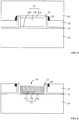
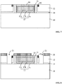
- Figures 1-9 show schematic views of semiconductor structures corresponding to certain stages of the exemplary fabrication method consistent with various disclosed embodiments.
- a dummy gate structure and a first dielectric layer surrounding the dummy gate structure may be formed on a semiconductor substrate and a source/drain region may be formed in the semiconductor substrate on each side of the dummy gate structure (S101).
- Figure 1 shows a schematic cross-section view of the semiconductor structure.
- a semiconductor substrate 10 is provided.
- a dummy gate structure 11 and a first dielectric layer 12 surrounding the dummy gate structure 11 may be formed on the surface of the semiconductor substrate 10.
- the top surface of the first dielectric layer 12 may be leveled with the top surface of the dummy gate structure 11.
- the semiconductor substrate 10 may be made of Si, Ge, silicon on insulator (SIO), etc.
- the dummy gate structure 11 may include a dummy gate insulating layer 11a formed on the semiconductor substrate 10 and a dummy gate electrode 11b formed on the top of the dummy gate insulating layer 11 a.
- the dummy gate insulating layer 11a may be made of SiO 2 while the dummy gate electrode 11b may be made of doped or un-doped polycrystalline silicon.
- the dummy gate insulating layer 11a and the dummy gate electrode 11b may be fabricated by a same process for forming gate insulating layers and gate electrodes of transistors in other regions. That is, the dummy gate insulating layer 11a and the dummy gate electrode 11b may be simultaneously formed with gate insulating layers and gate electrodes of transistors in other regions.
- An offset spacer 13 may be formed on each side of the dummy gate structure 11.
- the offset spacer 13 may be made of SiN.
- the offset spacer 13 may be used to increase the length of the channel region in order to avoid short channel effect.
- a source region and a drain region (not shown) may also be formed in the semiconductor substrate 10 on the two sides of the dummy gate structure 11.
- a contact-via etch stop layer 14 may be formed between the first dielectric layer 12 and the dummy gate structure 11 and also between the first dielectric layer 12 and the semiconductor substrate 10.
- the contact-via etch stop layers 14 may be made of SiN.
- the contact-via etch stop layers 14 may be used to determine the etch termination point for forming contact vias in the source/drain regions during a subsequent dry etching process.
- a top portion of the first dielectric layer may be removed to expose a portion of the dummy gate structure (S102).
- Figure 2 shows the corresponding semiconductor structure.
- a top portion of the first dielectric layer 12 is removed. With the top portion of the first dielectric layer 12 is removed, a portion of the dummy gate structure 11 and a portion of each offset spacer 13 formed on a side surface of the dummy gate structure 11 may exceed the level of the top surface of the remaining portion of the first dielectric layer 12.
- the portion of the first dielectric layer 12 may be removed by a photolithography process followed by a dry etching process.
- a contact-via etch stop layer 14 is formed between the first dielectric layer 12 and the dummy gate structure 11, after removing the portion of the first dielectric layer 12, a portion of each contact-via etch stop layer 14 formed on the corresponding offset spacer 13 on a sidewall surface of the dummy gate structure 11 may be exposed.
- a sidewall may be formed on each side surface of the exposed portion of the dummy gate structure (S103).
- Figure 2 shows a schematic cross-section view of the semiconductor structure with a sidewall 15 formed on each side of the exposed dummy gate structure 11.
- a sidewall material layer may be formed on the top surface of the remaining portion of the first dielectric layer 12, the top surface of the dummy gate structure 11, and the side surfaces of the exposed portion of the dummy gate structure 11.
- An etch-back process may then be performed on the sidewall material layer to form two sidewalls 15 to surround the exposed top portion of the dummy gate structure 11.
- the sidewall material layer may be made of at least one of SiN x , SiON, SiOBN, and SiOCN.
- the sidewall material layer may be made of a material with a relatively low etching rate. Specifically, the etching rate on the sidewall material layer may be lower than the etching rate on the first dielectric layer 12.
- the sidewall material layer may be made of an atomic layer deposition (ALD) process or a chemical vapor deposition (CVD) process.
- the material of the first dielectric layer may be deposited again to cover the top surface of the remaining portion of the previous first dielectric layer, the side surfaces of the sidewalls, and the top surface of the dummy gate structure (S104).
- deposition of the material of the first dielectric layer 12 may be resumed to let the first dielectric layer 12 cover the top surface of the remaining portion of the previous first dielectric layer 12, the side surface of the sidewalls 15, and the top surface of the dummy gate structure 11.
- the first dielectric layer 12 is made of SiO 2 .
- the first dielectric layer 12 may be formed by a CVD method using silane or tetraethyl orthosilicate (TEOS).
- TEOS tetraethyl orthosilicate
- the dielectric material of the first dielectric layer 12 is further deposited onto the top surface of the remaining first dielectric layer 12 until the top surface of the formed first dielectric layer 12 exceeds the top surface of the dummy gate structure 11.
- each sidewall may be removed through a planarization process to form an etch stop sidewall with a top surface leveled with the top surfaces of the first dielectric layer and the dummy gate structure (S105).
- Figure 3 shows a cross-section view of the corresponding semiconductor structure.
- a planarization process may be performed on the first dielectric layer 12, the sidewalls 15, and the dummy gate structure 11.
- a portion of each sidewall 15 (referring to Figure 2 ) may be removed to form an etch stop sidewall 16.
- a portion of the dummy gate structure 11 as well as a portion of the first dielectric layer 12 may also be removed.
- the top surface of the etch stop sidewalls 16 may be leveled with the top surface of the dummy gate structure 11 and the top surface of the first dielectric layer 12.
- a planarization process is performed on the first dielectric layer 12, the sidewalls 15, and the dummy gate structure 11 to remove the top sharp tips of the sidewalls 15 and ensure a certain width for the top surface of each sidewall 15.
- the planarization process may be a chemical mechanical polishing (CMP) process.
- the dummy gate structure 11 may also include, from bottom to top, a dummy gate insulating layer 11a, a dummy gate electrode 11b, and a dummy gate structure hard mask layer 11c.
- the dummy gate insulating layer 11a and the dummy gate electrode 11b may be formed by a dry etching process performed on a dummy gate insulating material layer (not shown) and a dummy gate electrode material layer using the dummy gate structure hard mask layer 11 c as an etch mask.
- the dummy gate structure hard mask layer 11c may be made of one of SiN x , SiON, etc.
- the dummy gate structure hard mask layer 11c may have the following advantages: as shown in Figure 5 , when performing a CMP process on the first dielectric layer 12 and the sidewalls 15, the dummy gate structure hard mask layer 11c may serve as a polish stop layer to define the termination point for the polishing process. Therefore, the termination point may be easily controlled and, thus, consumption of the dummy gate electrode 11b may be greatly avoided.
- the dummy gate structure may be removed to form a first trench (S106).
- Figure 6 shows a schematic cross-section view of the corresponding semiconductor structure.
- the dummy gate structure 11 (referring to Figure 3 ) is removed to form a first trench (not labeled).
- the first trench may expose a portion of the surface of the semiconductor substrate 10.
- a high-k dielectric layer, a work function layer, and a metal gate may be sequentially deposited to partially fill the first trench, leaving the top portion of the first trench become a second trench (S107).
- a high-k dielectric layer 17a, a work function layer 17b, and a metal gate 17c may be sequentially formed to fill the first trench. Further, a top portion of the high-k dielectric layer 17a, the work function layer 17b, and the metal gate 17c may then be removed to form a second trench 18. That is, the second trench 18 may be a top portion of the first trench formed before filling the high-k dielectric layer 17a, the work function layer 17b, and the metal gate 17c. Therefore, the bottom surface of the second trench 18 may be below the top surfaces of the first dielectric layer 12, the etch stop sidewalls 16, the contact-via etch stop layers 14, and the offset spacers 13. In addition, the portion of the materials formed outside of the first trench during the formation of the high-k dielectric layer 17a, the work function layer 17b, and the metal gate 17c may also be removed.
- the high-k dielectric layer 17a, the work function layer 17b, and the metal gate 17c together may form a metal gate structure 17.
- the high-k dielectric layer 17a may be made of at least one of La 2 O 3 , BaZrO 3 , HfZrO, HfZrON, HfLaO, HfSiO, HfSiON, LaSiO, AlSiO, HfTaO, HfTiO, BaO, TiO, Ti 2 O 3 , TiO 2 , SrO, Al 2 O 3 , Si 3 N 4 , etc.
- the work function layer 17b may be made of one or more of Ti, Al, Ti x Al 1-x , TiC, TiAlC, etc.
- the metal gate 17c may be made of W.
- Each of the high-k dielectric layer 17a, the work function layer 17b, and the metal gate 17c may be formed by a physical vapor deposition (PVD) process or a CVD process.
- PVD physical vapor deposition
- CVD chemical vapor deposition
- the portion of the materials of the above layers formed outside of the first trench may be removed by a CMP process.
- a top portion of the high-k dielectric layer 17a, the work function layer 17b, and the metal gate 17c formed in the first trench may be removed by a dry etching process or a wet etching process to form the second trench 18.
- the etching gas when a dry etching process is performed, the etching gas may contain SF 6 together with one or more of CF 4 , CHF 3 , C 3 F 8 , etc., or contain Cl 2 together with one or more of CF 4 , CHF 3 , C 3 F 8 , etc.
- the etching solution may include HF or any other appropriate acid.
- the etching solution may be a mixture of NH 4 OH, H 2 O 2 , and water (for example, a volume ratio of 1:1:5 for a 25% wt.
- an etch stop layer may be formed to fill up the second trench (S108).
- Figure 7 shows a schematic cross-section view of the corresponding semiconductor structure.
- an etch stop layer 19 may be formed to fill up the second trench 18.
- the top surface of the etch stop layer 19 may be leveled with the top surface of the first dielectric layer 12 and the top surface of the etch stop sidewalls 16.
- the material of the etch stop layer 19 may be different from the material of the first dielectric layer 12.
- the etch stop layer 19 is made of a material with a relatively low etching rate. That is, the etching rate on the etch stop layer 19 may be lower than the etching rate on the first dielectric layer 12.
- the etch stop layer 19 may be made of a same material as that used to form the etch stop sidewalls 16. That is, both the etch stop layer 19 and the etch stop sidewalls 16 may be made of a same insulating material.
- the etch stop layer 19 may be made of one or more of SiN x , SiON, SiOBN, SiOCN, etc.
- the etch stop layer 19 may be formed by an ALD process or a CVD process.
- the material formed outside of the second trench 18 during the formation of the etch stop layer 19 may be removed by a CMP process.
- a patterned mask layer may be formed on the top surfaces of the first dielectric layer, the etch stop layer, and the etch stop sidewalls (S109).
- Figure 8 shows a schematic cross-section view of the corresponding semiconductor structure with a patterned mask layer 20 formed on the first dielectric layer, the etch stop layer, and the etch stop sidewalls.
- a patterned mask layer 20 may be formed on the top surfaces of the first dielectric layer 12, the etch stop layer 19, and the etch stop sidewalls 16.
- an opening (not labeled) may be formed in the patterned mask layer 20 to expose a portion of the first dielectric layer 12.
- the opening may also expose a portion of the etch stop layer 19 and the corresponding etch stop sidewall 16.
- the patterned mask layer 20 may be made of photoresist and formed though a photolithography process.
- the patterned mask layer 20 may also be a hard mask layer made of a hard material such as SiN x , SiON, etc.
- the patterned hard mask layer may be formed by transferring a pattern of a photoresist layer to the hard mask layer.
- An opening may be formed in the patterned mask layer 20 on each side of the metal gate structure 17. The position of each opening may correspond to the position of the subsequently-formed via 21 in the corresponding source/drain region.
- the dimension of the opening formed in the patterned mask layer 20 may be larger than the desired dimension of the via 21 to be formed.
- the alignment error between the photomask plate and the substrate may also cause a considerable offset on the defined position of the opening in the patterned mask layer 20.
- the vias 21 may then be formed by etching the first dielectric layer 12, the etch stop sidewalls 16, and the etch stop layer 19 using such a patterned mask layer 20 with oversized and/or shifted openings as an etch mask.
- the etch stop layer 19 and the etch stop sidewalls 16 may provide protection for the metal gate structure 17 and the first dielectric layer 12, the metal gate 17c may not be exposed by the vias 21.
- subsequently-formed contact plugs by filling the vias 21 with a conductive material may not be electrically connected to the metal gate 17c.
- a via may be formed in the first dielectric layer on each side of the metal gate structure by etching the first dielectric layer, the etch stop layer, and the etch stop sidewalls (S110).
- an etching process may be performed on the exposed portion of the first dielectric layer 12, the etch stop layer 19, and the etch stop sidewalls 16 using the patterned mask layer 20 as an etch mask.
- a via 21 may then be formed in the first dielectric layer 12 on each side of the metal gate structure 17. Because of the substantially low etching rate on the etch stop layer 19 and the etch stop sidewalls 16, the etch stop layer 19 and the etch stop sidewalls 16 may only be slightly etched during the formation of the vias 21 in the first dielectric layer 12.
- a contact-via etch stop layer 14 may be formed on the surface of the semiconductor substrate 10. During the etching process to form the vias 21, because the etching rate on the contact-via etch stop layer 14 may be significantly lower than the etching rate on the first dielectric layer 12, the contact-via etch stop layer 14 may then be used to define the termination point of the etching process. Specifically, the etching process may be stopped once the surface of the source/drain region is exposed.
- a conductive material may be used to fill the vias to form contact plugs in the corresponding source/drain regions (S111).
- Figure 9 shows a schematic cross-section view of the corresponding semiconductor structure.
- contact plugs 22 may be formed by filling the vias 21 in the first dielectric layer 12 with a conductive material.
- the conductive material used to fill the vias 21 may be one of Cu, Al, W, etc.
- the vias 21 may not expose the metal gate 17c due to the protection of the etch stop layer 19 and the etch stop sidewalls 16, the contact plugs 22 formed by filling the vias 21 with a conductive material may not be electrically connected to the metal gate 17c. Therefore, the presence of the etch stop layer 19 and the etch stop sidewalls 16 may improve the device yield. In addition, due to the existence of the etch stop layer 19 and the etch stop sidewalls 16, the required alignment accuracy between the mask plate and the substrate may be reduced while the required precision for the photomask in the photolithography process to form the opening may also be reduced.
- Figure 10 and Figure 11 show schematic views of semiconductor structures of source/drain regions of a metal gate transistor corresponding to certain stages of another exemplary fabrication method consistent with disclosed embodiments. Specifically, Figure 10 and Figure 11 show schematic cross-section views of semiconductor structures fabricated based on the semiconductor structure shown in Figure 7 .
- a second dielectric layer 23 may be formed on the top surfaces of the etch stop layer 19, the first dielectric layer 12, and the etch stop sidewalls 16.
- a patterned mask layer 20 may then be formed on the top surface of the second dielectric layer.
- a via 21 may be formed on each side of the metal gate structure 17 through a dry etching process using the patterned mask layer 20 as an etch mask. Each via 21 may correspond to a source/drain region.
- an opening may be formed in the patterned mask layer 20 on each side of the metal gate structure 17.
- the position of each opening may correspond to a via to be formed in the corresponding source/drain region.
- a dry etching process using the patterned mask layer 20 as an etch mask may be performed to etch through the second dielectric layer 23.
- the etching process may continue to etch through the first dielectric layer 12 until the contact-via etch stop layer 14 is completely removed and the surface of the corresponding source/drain region is exposed.
- a portion of the etch stop layer 19 and the etch stop sidewalls 16 may also be slightly etched.
- the dimension of the opening formed in the patterned mask layer 20 may be larger than the desired dimension of the via 21 to be formed.
- the alignment error between the photomask plate and the substrate may also cause a considerable offset on the defined position of the opening in the patterned mask layer 20.
- the vias 21 may then be formed by etching the first dielectric layer 12, the etch stop sidewalls 16, and the etch stop layer 19 using such a patterned mask layer 20 with oversized and/or shifted openings as an etch mask.
- the etch stop layer 19 and the etch stop sidewalls 16 may provide protection for the metal gate structure 17 and the first dielectric layer 12, the metal gate 17c may not be exposed by the vias 21.
- subsequently-formed contact plugs 22 (referring to Figure 11 ) by filling the vias 21 with a conductive material may not be electrically connected to the metal gate 17c.
- a patterned mask layer (not shown) used to form a metal gate contact plug (not shown) may be formed on the second dielectric layer 23.
- a via corresponding to the metal gate 17c may be formed by etching through the second dielectric layer 23 and the etch stop layer 19 using the patterned mask layer as an etch mask. The via formed above the metal gate 17c may then be filled with a conductive material to form a contact plug for the metal gate 17c.
- the transistors described in the above embodiments are planar transistors.
- the method of forming an etch stop layer to cover the metal gate structure and an etch stop sidewall on each end of the etch stop layer may also be applicable to the fabrication of Fin-FETs.
- the method may improve device yield, reduce the required accuracy in aligning the mask plate and the substrate, and reduce the required dimension precision in the photolithography process.
- the dummy gate structure 11 may need to be removed before back filling the high-k dielectric layer 17a, the work function layer 17b, and the metal gate 17c to form the metal gate structure 17. Therefore, the fabrication process is a high-k last, metal gate last process.
- the method to form an etch stop layer 19 on the metal gate structure 17 with each of the two ends matching with the corresponding end of the metal gate structure 17 and form an etch stop sidewall 16 on each end of the etch stop layer 19 may also be adopted in a high-k first, metal gate last process in order to improve the device yield, reduce the required accuracy in aligning the mask plate and the substrate, and reduce the required dimension precision in the photolithography process.
- Figure 12 and Figure 13 show schematic cross-section views of the semiconductor structures corresponding to certain stages of an exemplary method using a high-k first, metal gate last process to fabricate a metal gate transistor consistent with disclosed embodiments.
- the differences between the embodiments corresponding to Figures 1-11 and the embodiments corresponding to Figure 12 and Figure 13 are illustrated.
- a semiconductor substrate 10 is provided. Different from the semiconductor substrate 10 shown in Figure 1 , a high-k dielectric layer 17a may be formed on the surface of the semiconductor substrate 10 and a dummy gate electrode 11b may then be formed on the high-k dielectric layer 17a. Further, a first dielectric layer 12 may be formed to surround the high-k dielectric layer 17a and the dummy gate electrode 11b with the top surface of the first dielectric layer 12 leveled with the top surface of the dummy gate electrode 11b.
- a high-k dielectric layer 17a, a dummy gate electrode 11b, and a dummy gate hard mask layer may be sequentially formed on the top surface of the semiconductor substrate 10. That is, an additional dummy gate hard mask layer may be formed on the dummy gate electrode 11b. Accordingly, a first dielectric layer 12 may be formed to surround the high-k dielectric layer 17a, the dummy gate electrode 11b, and the dummy gate hard mask layer.
- the high-k dielectric layer 17a may not be removed after forming the etch stop sidewalls 16. That is, only the dummy gate electrode 11b may be removed. Further, a first trench may be formed by removing the dummy gate electrode 11b. Then, a work function layer 17b and a metal gate 17c may be sequentially filled in to the first trench.
- a top portion of the material filled in the first trench may be removed to form a second trench above the metal gate structure 17 and an etch stop layer 19 may then be formed by back filling the second trench.
- the material removed from the top of the first trench is a portion of the work function layer 17b and the metal gate 17c.
- the portion of the work function layer 17b and the metal gate 17c may be removed by a dry etching process or a wet etching process. When a dry etching process is performed, the etching gas may be SF 6 or Cl 2 .
- the etching solution may be a mixture of NH 4 OH, H 2 O 2 , and water (for example, a volume ratio of 1:1:5 for a 25% wt. NH 4 OH solution, H 2 O 2 , and H 2 O), or a mixture of HCl, H 2 O 2 , and water (for example, a volume ratio of 1:1:6 for pure HCl acid, H 2 O 2 , and H 2 O).
- a patterned mask layer 20 may be formed on the top surfaces of the etch stop layer 19, the first dielectric layer 12, and the etch stop sidewalls 16.
- An opening may be formed in the patterned mask layer 20 on each side of the metal gate structure 17 with the position of the opening corresponding to the position of a contact via 21 in the corresponding source/drain region.
- a via 21 may then be formed in the first dielectric layer on each side of the metal gate structure 17 through a dry etching process using the patterned mask layer 20 as an etch mask.
- a second dielectric layer 23 may be first formed on the top surfaces of the etch stop layer 19, the first dielectric layer 12, and the etch stop sidewalls 16.
- a patterned mask layer 20 may then be formed on the second dielectric layer 23.
- An opening may be formed in the patterned mask layer 20 on each side of the metal gate structure 17 with the position of the opening corresponding to the position of a contact via 21 in the corresponding source/drain region.
- a via 21 may then be formed in the first dielectric layer on each side of the metal gate structure 17 through a dry etching process using the patterned mask layer 20 as an etch mask to etch the second dielectric layer 23, the etch stop layer 19, the etch stop sidewalls 16, and the first dielectric layer 12.
- the high-k first, metal gate last process may also be applicable to the fabrication of fin-FET transistors.
- the present invention also provides a metal gate transistor.
- the metal gate transistor includes a semiconductor substrate 10, a metal gate structure 17 formed on the semiconductor substrate 10, and a first dielectric layer 12 surrounding the metal gate structure 17.
- the metal gate structure further includes a high-k dielectric layer 17a formed on the surface of the semiconductor substrate 10, a work function layer 17b formed on the surface of the high-k dielectric layer 17a, and a metal gate 17c formed on the surface of the work function layer 17b.
- the metal gate structure 17 is covered by an etch stop layer 19.
- An etch stop sidewall 16 is formed on each end of the etch stop layer 19.
- the disclosed metal gate transistor also includes a source/drain region in the semiconductor substrate on each side of the metal gate structure 17.
- a contact plug 22 is formed in the first dielectric layer 12.
- the contact plug 22 is electrically isolated from the metal gate structure 17 due to the presence of the etch stop layer 19 and the etch stop sidewalls 16.
- the first dielectric layer 12, the contact plugs 22, the etch stop sidewalls 16, and the etch stop layer 19 may all have a coplanar top surface.
- the vias 21 formed through a dry etching process using the patterned mask layer 20 as an etch mask may not expose the metal gate 17c because of the protection provided by the etch stop layer 19 and the etch stop sidewalls 16. Therefore, the contact plugs 22 formed subsequently by filling up the vias 21 with a conductive material may not be electrically connected to the metal gate 17c. As such, the device yield may be improved, the required alignment accuracy between the mask plate and the substrate may be reduced, and the required dimension precision in the photolithography process may also be reduced.
- the disclosed metal gate transistor and fabrication method may demonstrate several advantages.
- an etch stop layer may be formed to cover the metal gate structure with each end of the etch stop layer matching with the corresponding end of the metal gate structure; in addition, an etch stop sidewall may also be formed on each end of the etch stop layer.
- the etch stop layer may be formed after the dummy gate structure is removed and the high-k dielectric layer, the work function layer, and the metal gate are filled in; while for a high-k first, metal gate last process, the etch stop layer may be formed after the dummy gate electrode is removed and the work function layer and the metal gate are filled in.
- the etch stop layer and the etch stop sidewalls may be made of an insulating material different from the material used to form the dielectric layer which surrounds the metal gate structure.
- the etch stop layer and the etch stop sidewalls may provide protection for the metal gate structure and the dielectric layer. Therefore, the vias formed by the dry etching process may not expose the metal gate despite a potential alignment offset between the mask plate and the substrate and/or oversized openings formed in the mask plate corresponding to the vias.
- the conductive material may not be electrically connected to the metal gate.
- the device yield may be improved, the required alignment accuracy between the mask plate and the substrate may be reduced, and the required dimension precision in the photolithography process may also be reduced.
- the top surface of the etch stop layer and the top surface of the etch stop sidewalls may be leveled with the top surface of the dielectric layer that covers the metal gate. Further, after forming the etch stop layer and the etch stop sidewalls to protect the metal gate structure and the dielectric layer, several fabrication methods are provided to form electrical connections for the source/drain regions and the metal gate and to complete the metal gate transistor.
- one method to complete the metal gate transistor may include forming a patterned mask layer on the top surfaces of the etch stop sidewalls, the etch stop layer, and the dielectric layer.
- the openings formed in the patterned mask layer may correspond to the contact vias to be formed in the source/drain regions.
- the method may further include forming the vias by etching the etch stop layer, the etch stop sidewalls, and the dielectric layer using the mask layer as an etch mask and then forming contact plugs for the source/drain regions by filling up the vias with a conductive material.
- the method may also include forming an upper-level dielectric layer (i.e., a second dielectric layer) over the contact plugs, the dielectric layer, the etch stop layer, and the etch stop sidewalls, and then forming upper-level vias by etching the upper-level dielectric layer using an etch mask.
- the upper-level vias formed in the upper-level dielectric layer may be aligned with the contact plugs in the source/drain regions or may expose the metal gate.
- the method may include forming conductive plugs electrically connected to the metal gate or the source/drain regions by filling up the upper-level vias with a conductive material.
- another method to complete the metal gate transistor may include forming an upper-level dielectric layer on the top surfaces of the etch stop sidewalls, the etch stop layer, and the dielectric layer, and then forming a patterned mask layer on the upper-level dielectric layer.
- the openings formed in the patterned mask layer may correspond to the contact vias to be formed in the source/drain regions.
- the method may then include forming the contact vias for the source/drain regions by etching the upper-level dielectric layer, the etch stop layer, the etch stop sidewalls, and the dielectric layer using the patterned mask layer as an etch mask, and then forming contact plugs in the source/drain regions by filling up the contact vias with a conductive material.
- the method may further include forming another patterned mask layer on the upper-level dielectric layer in order to form a contact plug for the metal gate. That is, the opening formed in the patterned mask layer may correspond to the metal gate.
- the method may include forming a via by etching the upper-level dielectric layer using the patterned mask layer as an etch mask, and then forming the contact plug for the metal gate by filling up the via with a conductive material.
- the disclosed metal gate transistor may be a planar transistor or a Fin-FET. Therefore, the disclosed metal gate transistor and the fabrication method may have a broad scope of application.
Landscapes
- Chemical & Material Sciences (AREA)
- Insulated Gate Type Field-Effect Transistor (AREA)
- Electrodes Of Semiconductors (AREA)
- Chemical Kinetics & Catalysis (AREA)
- Engineering & Computer Science (AREA)
- Composite Materials (AREA)
- Materials Engineering (AREA)
- Internal Circuitry In Semiconductor Integrated Circuit Devices (AREA)
Abstract
Description
- This application claims the priority of Chinese Patent Application No.
CN201511001045.1, filed on December 28,2015 - The present invention generally relates to the field of semiconductor fabrication technology and, more particularly, relates to a metal gate transistor and fabrication methods thereof.
- For semiconductor manufacturing, especially for very large scale integrated (VLSI) circuits, the main device component is metal-oxide-semiconductor field-effect transistor (MOSFET). Since the invention of MOSFET, the geometric size of MOSFET has been continuously reduced following the Moore's law. However, the physical limits of devices may lead to increasing challenges in continuously scaling down the devices. Specifically, in the field of MOSFET manufacturing, the challenging aspect is a current leaking problem due to decreases in the thicknesses of the polycrystalline Si layer and the SiO2 dielectric layer in the traditional MOS technology as the devices are scaled down.
- Aimed to solve the above problems, the current technology uses high-k (dielectric constant or permittivity) dielectric material to replace the traditional SiO2 dielectric material. In the meantime, the current technology also uses metal gate to match with the high-k dielectric material.
- According to existing methods, during the formation of contact plugs in source/drain regions of a metal gate transistor, a number of factors, such as the size of the via and the overlay (OVL) offset in aligning the photomask and the substrate, may cause a short circuit between the metal gate and the formed contact plug in the source/drain region, which may reduce device yield. On the other hand, the size of the via and the OVL offset in aligning the photomask and the substrate may be reduced in order to improve device yield, but process cost may also be increased.
- The disclosed fabrication method and metal gate transistor are directed to solve one or more problems set forth above and other problems in the art.
- A first aspect of the present invention includes a method for fabricating a metal gate transistor. The method includes forming a dummy gate structure and a first dielectric layer on a semiconductor substrate and a source/drain region in the semiconductor substrate on each side of the dummy gate structure. The dummy gate structure is surrounded by the first dielectric layer and the top surface of the dummy gate structure is leveled with the top surface of the first dielectric layer. The method then includes forming an etch stop sidewall in the first dielectric layer on each side of the dummy gate structure. The top surface of the etch stop sidewall is leveled with the top surfaces of the first dielectric layer and the dummy gate structure. The method further includes forming a first trench by removing the dummy gate structure, and forming a metal gate structure to partially fill the first trench. The top portion of the first trench becomes a second trench. Further, the method also includes forming an etch stop layer by filling the second trench, and forming a contact plug in the first dielectric layer to electrically connect to each source/drain region.
- Forming the etch stop sidewall in the first dielectric layer on each side of the dummy gate structure may further include: removing a top portion of the first dielectric layer to expose a portion of the dummy gate structure; forming a sidewall on each side surface of the exposed portion of the dummy gate structure; depositing a material of the first dielectric layer to cover the dummy gate structure, the sidewalls, and a remaining portion of the first dielectric layer; and forming the etch stop sidewall on each side of the dummy gate structure by removing a top portion of the corresponding sidewall.
- Forming the metal gate structure to partially fill the first trench may further include: sequentially filling a high-k dielectric layer, a work function layer, and a metal gate into the first trench; and removing a top portion of the high-k dielectric layer, the work function layer, and the metal gate.
- Forming the contact plug to electrically connect to each source/drain region may further include: forming a patterned mask layer on the top surfaces of the first dielectric layer, the etch stop layer, and the etch stop sidewalls, wherein an opening is formed in the patterned mask layer corresponding to each source/drain region; forming a via in the semiconductor substrate corresponding to each source/drain region by etching the first dielectric layer, the etch stop layer, and the etch stop sidewalls using the patterned mask layer as an etch mask; and forming the contact plug to electrically connect to each source/drain region by filling the corresponding via with a conductive material.
- After forming the etch stop layer, a second dielectric layer may be formed on the top surfaces of the etch stop layer, the first dielectric layer, and the etch stop sidewalls, and coordinately. Then, the patterned mask layer may be formed on the top surface of the second dielectric layer. Further, the vias may be formed in the first dielectric layer and the second dielectric layer by etching the second dielectric layer, the first dielectric layer, the etch stop layer, and the etch stop sidewalls using the patterned mask layer as an etch mask.
- Preferably, the first dielectric layer is separated from the dummy gate structure and the semiconductor substrate by contact-via etch stop layers.
- Preferably, an offset spacer is formed on each side of the dummy gate structure.
- Preferably, the dummy gate structure includes a dummy gate insulating layer formed on the semiconductor substrate and a dummy gate electrode formed on the top of the dummy gate insulating layer. The dummy gate structure may further include a dummy gate structure hard mask layer formed on the dummy gate electrode.
- The etch stop sidewalls may be made of at least one of SiNx, SiON, SiOBN, SiOCN.
- Preferably, the etch stop sidewalls are formed by an atomic layer deposition or a chemical vapor deposition method.
- The etch stop layer may be made of at least one of SiNx, SiON, SiOBN, SiOCN.
- Preferably, the etch stop layer is formed by an atomic layer deposition or a chemical vapor deposition method.
- For example, the metal gate transistor is a planar FET or a fin-FET.
- A second aspect of the present invention provides an alternative method for fabricating the metal gate transistor. The method includes forming a high-k dielectric layer on a semiconductor substrate and a dummy gate electrode on the high-k dielectric layer. The method also includes forming a source/drain region in the semiconductor substrate on each side of the high-k dielectric layer and a first dielectric layer on the semiconductor substrate to surround the high-k dielectric layer and the dummy gate electrode. The top surface of the dummy gate electrode is leveled with the top surface of the first dielectric layer. Further, the method includes forming an etch stop sidewall in the first dielectric layer on each side of the dummy gate electrode. The top surface of the etch stop sidewall is leveled with the top surfaces of the first dielectric layer and the dummy gate electrode. Moreover, the method includes forming a first trench by removing the dummy gate electrode, and forming a metal gate structure to partially fill the first trench. The high-k dielectric layer is the dielectric layer of the formed metal gate structure and a top portion of the first trench becomes a second trench. Finally, the method also includes forming an etch stop layer to fill the second trench, and forming a contact plug in the first dielectric layer to electrically connect to each source/drain region.
- Forming the etch stop sidewall in the first dielectric layer on each side of the dummy gate electrode may further include: removing a top portion of the first dielectric layer to expose a portion of the dummy gate electrode; forming a sidewall on each side surface of the exposed portion of the dummy gate electrode; depositing a material of the first dielectric layer to cover the dummy gate electrode, the sidewalls, and a remaining portion of the first dielectric layer; and forming the etch stop sidewall on each side of the dummy gate electrode by removing a top portion of the corresponding sidewall.
- Forming the metal gate structure to partially fill the first trench may further include: sequentially filling a work function layer and a metal gate into the first trench; and removing a top portion of the work function layer and the metal gate.
- Forming the contact plug to electrically connect to each source/drain region may further include: forming a patterned mask layer on the top surfaces of the first dielectric layer, the etch stop layer, and the etch stop sidewalls, wherein an opening is formed in the patterned mask layer corresponding to each source/drain region; forming a via in the semiconductor substrate corresponding to each source/drain region by etching the first dielectric layer, the etch stop layer, and the etch stop sidewalls using the patterned mask layer as an etch mask; and forming the contact plug to electrically connect to each source/drain region by filling the corresponding via with a conductive material.
- After forming the etch stop layer, a second dielectric layer may be formed on the top surfaces of the etch stop layer, the first dielectric layer, and the etch stop sidewalls, and coordinately. Then, the patterned mask layer may be formed on the top surface of the second dielectric layer. Further, the vias may be formed in the first dielectric layer and the second dielectric layer by etching the second dielectric layer, the first dielectric layer, the etch stop layer, and the etch stop sidewalls using the patterned mask layer as an etch mask.
- In the method for fabricating the metal gate transistor of any one of the first and second aspect of the invention, the following is applicable.
- The high-k dielectric layer may be made of at least one of La2O3, BaZrO3, HfZrO, HfZrON, HfLaO, HfSiO, HfSiON, LaSiO, AlSiO, HfTaO, HfTiO, BaO, TiO, Ti2O3, TiO2, SrO, Al2O3, Si3N4.
- The work function layer may be made of at least one of Ti, Al, TixAl1-x, TiC, TiAlC.
- The metal gate may be made of W.
- Preferably, a dry etching process is performed to remove the top portion of the high-k dielectric layer, the work function layer, and the metal gate, an etching gas containing at least one of CF4, CHF3, and C3F8, together with SF6, or contains at least one of CF4, CHF3, and C3F8, together with Cl2 is used.
- Preferably, when a wet etching process is performed to remove the top portion of the high-k dielectric layer, a HF acid solution is used as an etching solution while when a wet etching process is performed to remove the top portion of the work function layer and the metal gate, a mixture of NH4OH, H2O2, and water, or a mixture of HCl, H2O2, and water is used as a wet etching solution.
- A third aspect of the present invention provides a metal gate transistor. The metal gate transistor includes a semiconductor substrate, a metal gate structure including a high-k dielectric layer formed on the semiconductor substrate, a work function layer formed on the high-k dielectric layer, and a metal gate formed on the work function layer. The metal gate transistor also includes a first dielectric layer surrounding the metal gate structure, a source/drain region formed in the semiconductor substrate on each side of the metal gate structure, an etch stop layer formed on the metal gate structure with a top surface leveled with the top surface of the first dielectric layer, and an etch stop sidewall formed on each side of the metal gate structure. The top surface of the etch stop sidewall is leveled with the top surface of the first dielectric layer. Finally, the metal gate transistor includes a contact plug formed in the first dielectric layer to electrically connect to each source/drain region.
- The metal gate transistor may further include a second dielectric layer formed on the first dielectric layer, the etch stop layer, and the etch stop sidewalls. The contact plug connecting to each source/drain region may be formed in the first dielectric layer and the second dielectric layer.
- Other aspects of the present invention can be understood by those skilled in the art in light of the description, the claims, and the drawings of the present invention.
- The following drawings are merely examples for illustrative purposes according to various disclosed embodiments and are not intended to limit the scope of the present invention.
-
Figures 1-9 illustrate schematic views of semiconductor structures corresponding to certain stages of an exemplary fabrication method for a contact plug in a source/drain region of a metal gate transistor consistent with various disclosed embodiments; -
Figures 10-11 illustrate schematic views of semiconductor structures corresponding to certain stages of another exemplary fabrication method consistent with disclosed embodiments; -
Figures 12-13 illustrate schematic views of semiconductor structures corresponding to certain stages of another exemplary fabrication method consistent with disclosed embodiments; and -
Figure 14 illustrates a flowchart of the exemplary fabrication process consistent with disclosed embodiments. - Reference will now be made in detail to exemplary embodiments of the invention, which are illustrated in the accompanying drawings. Wherever possible, the same reference numbers will be used throughout the drawings to refer to the same or like parts.
- As described in the above background section, when using existing methods to fabricate contact plugs in source/drain regions of metal gate transistors, the product yield may be low. Further, according to existing methods, the accuracy in aligning mask plate with substrate and the dimension precision in the photolithography process may need to be improved in order to raise the product yield. However, improving the alignment accuracy may also result in increased process cost. In view of the above problems, the present invention provides an improved method to fabricated contact plugs in source/drain regions of metal gate transistors.
-
Figure 14 shows a flowchart of the exemplary process for fabricating a contact plug in each source/drain region of a metal gate transistor consistent with disclosed embodiments.Figures 1-9 show schematic views of semiconductor structures corresponding to certain stages of the exemplary fabrication method consistent with various disclosed embodiments. - Referring to
Figure 14 , at the beginning of the fabrication process, a dummy gate structure and a first dielectric layer surrounding the dummy gate structure may be formed on a semiconductor substrate and a source/drain region may be formed in the semiconductor substrate on each side of the dummy gate structure (S101).Figure 1 shows a schematic cross-section view of the semiconductor structure. - Referring to
Figure 1 , asemiconductor substrate 10 is provided. Adummy gate structure 11 and afirst dielectric layer 12 surrounding thedummy gate structure 11 may be formed on the surface of thesemiconductor substrate 10. The top surface of thefirst dielectric layer 12 may be leveled with the top surface of thedummy gate structure 11. - The
semiconductor substrate 10 may be made of Si, Ge, silicon on insulator (SIO), etc. Thedummy gate structure 11 may include a dummygate insulating layer 11a formed on thesemiconductor substrate 10 and adummy gate electrode 11b formed on the top of the dummygate insulating layer 11 a. In one embodiment, the dummygate insulating layer 11a may be made of SiO2 while thedummy gate electrode 11b may be made of doped or un-doped polycrystalline silicon. The dummygate insulating layer 11a and thedummy gate electrode 11b may be fabricated by a same process for forming gate insulating layers and gate electrodes of transistors in other regions. That is, the dummygate insulating layer 11a and thedummy gate electrode 11b may be simultaneously formed with gate insulating layers and gate electrodes of transistors in other regions. - An offset
spacer 13 may be formed on each side of thedummy gate structure 11. The offsetspacer 13 may be made of SiN. The offsetspacer 13 may be used to increase the length of the channel region in order to avoid short channel effect. Further, a source region and a drain region (not shown) may also be formed in thesemiconductor substrate 10 on the two sides of thedummy gate structure 11. In addition, a contact-viaetch stop layer 14 may be formed between thefirst dielectric layer 12 and thedummy gate structure 11 and also between thefirst dielectric layer 12 and thesemiconductor substrate 10. The contact-via etch stop layers 14 may be made of SiN. The contact-via etch stop layers 14 may be used to determine the etch termination point for forming contact vias in the source/drain regions during a subsequent dry etching process. - Returning to
Figure 14 , a top portion of the first dielectric layer may be removed to expose a portion of the dummy gate structure (S102).Figure 2 shows the corresponding semiconductor structure. - Referring to
Figure 2 , a top portion of thefirst dielectric layer 12 is removed. With the top portion of thefirst dielectric layer 12 is removed, a portion of thedummy gate structure 11 and a portion of each offsetspacer 13 formed on a side surface of thedummy gate structure 11 may exceed the level of the top surface of the remaining portion of thefirst dielectric layer 12. - The portion of the
first dielectric layer 12 may be removed by a photolithography process followed by a dry etching process. In one embodiment, because a contact-viaetch stop layer 14 is formed between thefirst dielectric layer 12 and thedummy gate structure 11, after removing the portion of thefirst dielectric layer 12, a portion of each contact-viaetch stop layer 14 formed on the corresponding offsetspacer 13 on a sidewall surface of thedummy gate structure 11 may be exposed. - Further, returning to
Figure 14 , a sidewall may be formed on each side surface of the exposed portion of the dummy gate structure (S103).Figure 2 shows a schematic cross-section view of the semiconductor structure with asidewall 15 formed on each side of the exposeddummy gate structure 11. - Referring to
Figure 2 , after removing the portion of thefirst dielectric layer 12, a sidewall material layer may be formed on the top surface of the remaining portion of thefirst dielectric layer 12, the top surface of thedummy gate structure 11, and the side surfaces of the exposed portion of thedummy gate structure 11. An etch-back process may then be performed on the sidewall material layer to form twosidewalls 15 to surround the exposed top portion of thedummy gate structure 11. - The sidewall material layer may be made of at least one of SiNx, SiON, SiOBN, and SiOCN. In one embodiment, the sidewall material layer may be made of a material with a relatively low etching rate. Specifically, the etching rate on the sidewall material layer may be lower than the etching rate on the
first dielectric layer 12. The sidewall material layer may be made of an atomic layer deposition (ALD) process or a chemical vapor deposition (CVD) process. - Returning to
Figure 14 , further, the material of the first dielectric layer may be deposited again to cover the top surface of the remaining portion of the previous first dielectric layer, the side surfaces of the sidewalls, and the top surface of the dummy gate structure (S104). - Specifically, deposition of the material of the
first dielectric layer 12 may be resumed to let thefirst dielectric layer 12 cover the top surface of the remaining portion of the previousfirst dielectric layer 12, the side surface of thesidewalls 15, and the top surface of thedummy gate structure 11. - In one embodiment, the
first dielectric layer 12 is made of SiO2. Thefirst dielectric layer 12 may be formed by a CVD method using silane or tetraethyl orthosilicate (TEOS). The dielectric material of thefirst dielectric layer 12 is further deposited onto the top surface of the remainingfirst dielectric layer 12 until the top surface of the formedfirst dielectric layer 12 exceeds the top surface of thedummy gate structure 11. - Further, returning to
Figure 14 , a portion of each sidewall may be removed through a planarization process to form an etch stop sidewall with a top surface leveled with the top surfaces of the first dielectric layer and the dummy gate structure (S105).Figure 3 shows a cross-section view of the corresponding semiconductor structure. - Referring to
Figure 3 , a planarization process may be performed on thefirst dielectric layer 12, thesidewalls 15, and thedummy gate structure 11. During the planarization process, a portion of each sidewall 15 (referring toFigure 2 ) may be removed to form anetch stop sidewall 16. In the meantime, a portion of thedummy gate structure 11 as well as a portion of thefirst dielectric layer 12 may also be removed. After the planarization process, the top surface of the etch stop sidewalls 16 may be leveled with the top surface of thedummy gate structure 11 and the top surface of thefirst dielectric layer 12. - In one embodiment, a planarization process is performed on the
first dielectric layer 12, thesidewalls 15, and thedummy gate structure 11 to remove the top sharp tips of thesidewalls 15 and ensure a certain width for the top surface of eachsidewall 15. The planarization process may be a chemical mechanical polishing (CMP) process. - In certain other embodiments, as shown in
Figure 4 , thedummy gate structure 11 may also include, from bottom to top, a dummygate insulating layer 11a, adummy gate electrode 11b, and a dummy gate structurehard mask layer 11c. The dummygate insulating layer 11a and thedummy gate electrode 11b may be formed by a dry etching process performed on a dummy gate insulating material layer (not shown) and a dummy gate electrode material layer using the dummy gate structurehard mask layer 11 c as an etch mask. The dummy gate structurehard mask layer 11c may be made of one of SiNx, SiON, etc. - Keeping the dummy gate structure
hard mask layer 11c may have the following advantages: as shown inFigure 5 , when performing a CMP process on thefirst dielectric layer 12 and thesidewalls 15, the dummy gate structurehard mask layer 11c may serve as a polish stop layer to define the termination point for the polishing process. Therefore, the termination point may be easily controlled and, thus, consumption of thedummy gate electrode 11b may be greatly avoided. - Further, returning to
Figure 14 , the dummy gate structure may be removed to form a first trench (S106).Figure 6 shows a schematic cross-section view of the corresponding semiconductor structure. - Referring to
Figure 6 , the dummy gate structure 11 (referring toFigure 3 ) is removed to form a first trench (not labeled). The first trench may expose a portion of the surface of thesemiconductor substrate 10. - Returning to
Figure 13 , further, a high-k dielectric layer, a work function layer, and a metal gate may be sequentially deposited to partially fill the first trench, leaving the top portion of the first trench become a second trench (S107). - Specifically, a high-
k dielectric layer 17a, awork function layer 17b, and ametal gate 17c may be sequentially formed to fill the first trench. Further, a top portion of the high-k dielectric layer 17a, thework function layer 17b, and themetal gate 17c may then be removed to form asecond trench 18. That is, thesecond trench 18 may be a top portion of the first trench formed before filling the high-k dielectric layer 17a, thework function layer 17b, and themetal gate 17c. Therefore, the bottom surface of thesecond trench 18 may be below the top surfaces of thefirst dielectric layer 12, the etch stop sidewalls 16, the contact-via etch stop layers 14, and the offsetspacers 13. In addition, the portion of the materials formed outside of the first trench during the formation of the high-k dielectric layer 17a, thework function layer 17b, and themetal gate 17c may also be removed. - The high-
k dielectric layer 17a, thework function layer 17b, and themetal gate 17c together may form ametal gate structure 17. The high-k dielectric layer 17a may be made of at least one of La2O3, BaZrO3, HfZrO, HfZrON, HfLaO, HfSiO, HfSiON, LaSiO, AlSiO, HfTaO, HfTiO, BaO, TiO, Ti2O3, TiO2, SrO, Al2O3, Si3N4, etc. Thework function layer 17b may be made of one or more of Ti, Al, TixAl1-x, TiC, TiAlC, etc. Themetal gate 17c may be made of W. - Each of the high-
k dielectric layer 17a, thework function layer 17b, and themetal gate 17c may be formed by a physical vapor deposition (PVD) process or a CVD process. The portion of the materials of the above layers formed outside of the first trench may be removed by a CMP process. - In one embodiment, after the deposition of the materials for the above layers and the subsequent removal of the portion of the materials deposited outside of the first trench, a top portion of the high-
k dielectric layer 17a, thework function layer 17b, and themetal gate 17c formed in the first trench may be removed by a dry etching process or a wet etching process to form thesecond trench 18. - Specifically, when a dry etching process is performed, the etching gas may contain SF6 together with one or more of CF4, CHF3, C3F8, etc., or contain Cl2 together with one or more of CF4, CHF3, C3F8, etc. When the portion of the high-
k dielectric layer 17a is removed by wet etching, the etching solution may include HF or any other appropriate acid. When the portion of thework function layer 17b and the portion of themetal gate 17c are removed by wet etching, the etching solution may be a mixture of NH4OH, H2O2, and water (for example, a volume ratio of 1:1:5 for a 25% wt. NH4OH solution, H2O2, and H2O), or a mixture of HCl, H2O2, and water (for example, a volume ratio of 1:1:6 for pure HCl acid, H2O2, and H2O). - Further, returning to
Figure 14 , an etch stop layer may be formed to fill up the second trench (S108).Figure 7 shows a schematic cross-section view of the corresponding semiconductor structure. - Referring to
Figure 7 , anetch stop layer 19 may be formed to fill up thesecond trench 18. The top surface of theetch stop layer 19 may be leveled with the top surface of thefirst dielectric layer 12 and the top surface of the etch stop sidewalls 16. - The material of the
etch stop layer 19 may be different from the material of thefirst dielectric layer 12. In one embodiment, theetch stop layer 19 is made of a material with a relatively low etching rate. That is, the etching rate on theetch stop layer 19 may be lower than the etching rate on thefirst dielectric layer 12. Moreover, theetch stop layer 19 may be made of a same material as that used to form the etch stop sidewalls 16. That is, both theetch stop layer 19 and the etch stop sidewalls 16 may be made of a same insulating material. - In one embodiment, the
etch stop layer 19 may be made of one or more of SiNx, SiON, SiOBN, SiOCN, etc. Theetch stop layer 19 may be formed by an ALD process or a CVD process. The material formed outside of thesecond trench 18 during the formation of theetch stop layer 19 may be removed by a CMP process. - Further, returning to
Figure 14 , a patterned mask layer may be formed on the top surfaces of the first dielectric layer, the etch stop layer, and the etch stop sidewalls (S109).Figure 8 shows a schematic cross-section view of the corresponding semiconductor structure with a patternedmask layer 20 formed on the first dielectric layer, the etch stop layer, and the etch stop sidewalls. - Referring to
Figure 8 , a patternedmask layer 20 may be formed on the top surfaces of thefirst dielectric layer 12, theetch stop layer 19, and the etch stop sidewalls 16. Corresponding to each side of themetal gate structure 17, an opening (not labeled) may be formed in the patternedmask layer 20 to expose a portion of thefirst dielectric layer 12. In addition, the opening may also expose a portion of theetch stop layer 19 and the correspondingetch stop sidewall 16. - In one embodiment, the patterned
mask layer 20 may be made of photoresist and formed though a photolithography process. In certain other embodiments, the patternedmask layer 20 may also be a hard mask layer made of a hard material such as SiNx, SiON, etc. The patterned hard mask layer may be formed by transferring a pattern of a photoresist layer to the hard mask layer. An opening may be formed in the patternedmask layer 20 on each side of themetal gate structure 17. The position of each opening may correspond to the position of the subsequently-formed via 21 in the corresponding source/drain region. - In certain circumstances, the dimension of the opening formed in the patterned
mask layer 20 may be larger than the desired dimension of the via 21 to be formed. In addition, the alignment error between the photomask plate and the substrate may also cause a considerable offset on the defined position of the opening in the patternedmask layer 20. In a subsequent process, thevias 21 may then be formed by etching thefirst dielectric layer 12, the etch stop sidewalls 16, and theetch stop layer 19 using such apatterned mask layer 20 with oversized and/or shifted openings as an etch mask. However, because theetch stop layer 19 and the etch stop sidewalls 16 may provide protection for themetal gate structure 17 and thefirst dielectric layer 12, themetal gate 17c may not be exposed by thevias 21. As a result, subsequently-formed contact plugs by filling thevias 21 with a conductive material may not be electrically connected to themetal gate 17c. - Further, using the patterned mask layer as an etch mask, a via may be formed in the first dielectric layer on each side of the metal gate structure by etching the first dielectric layer, the etch stop layer, and the etch stop sidewalls (S110).
- Referring to
Figure 8 , an etching process may be performed on the exposed portion of thefirst dielectric layer 12, theetch stop layer 19, and the etch stop sidewalls 16 using the patternedmask layer 20 as an etch mask. After the etching process, a via 21 may then be formed in thefirst dielectric layer 12 on each side of themetal gate structure 17. Because of the substantially low etching rate on theetch stop layer 19 and the etch stop sidewalls 16, theetch stop layer 19 and the etch stop sidewalls 16 may only be slightly etched during the formation of the vias 21 in thefirst dielectric layer 12. - In one embodiment, a contact-via
etch stop layer 14 may be formed on the surface of thesemiconductor substrate 10. During the etching process to form thevias 21, because the etching rate on the contact-viaetch stop layer 14 may be significantly lower than the etching rate on thefirst dielectric layer 12, the contact-viaetch stop layer 14 may then be used to define the termination point of the etching process. Specifically, the etching process may be stopped once the surface of the source/drain region is exposed. - Returning to
Figure 14 , after the formation of the vias in the first dielectric layer, a conductive material may be used to fill the vias to form contact plugs in the corresponding source/drain regions (S111).Figure 9 shows a schematic cross-section view of the corresponding semiconductor structure. - Referring to
Figure 9 , contact plugs 22 may be formed by filling thevias 21 in thefirst dielectric layer 12 with a conductive material. The conductive material used to fill thevias 21 may be one of Cu, Al, W, etc. - Because the
vias 21 may not expose themetal gate 17c due to the protection of theetch stop layer 19 and the etch stop sidewalls 16, the contact plugs 22 formed by filling thevias 21 with a conductive material may not be electrically connected to themetal gate 17c. Therefore, the presence of theetch stop layer 19 and the etch stop sidewalls 16 may improve the device yield. In addition, due to the existence of theetch stop layer 19 and the etch stop sidewalls 16, the required alignment accuracy between the mask plate and the substrate may be reduced while the required precision for the photomask in the photolithography process to form the opening may also be reduced. - Moreover, the present invention also provides additional fabrication methods. For example,
Figure 10 andFigure 11 show schematic views of semiconductor structures of source/drain regions of a metal gate transistor corresponding to certain stages of another exemplary fabrication method consistent with disclosed embodiments. Specifically,Figure 10 andFigure 11 show schematic cross-section views of semiconductor structures fabricated based on the semiconductor structure shown inFigure 7 . - Referring to
Figure 10 , after forming theetch stop layer 19 and the etch stop sidewalls 16, asecond dielectric layer 23 may be formed on the top surfaces of theetch stop layer 19, thefirst dielectric layer 12, and the etch stop sidewalls 16. A patternedmask layer 20 may then be formed on the top surface of the second dielectric layer. Further, a via 21 may be formed on each side of themetal gate structure 17 through a dry etching process using the patternedmask layer 20 as an etch mask. Each via 21 may correspond to a source/drain region. - Specifically, as shown in
Figure 10 , an opening may be formed in the patternedmask layer 20 on each side of themetal gate structure 17. The position of each opening may correspond to a via to be formed in the corresponding source/drain region. A dry etching process using the patternedmask layer 20 as an etch mask may be performed to etch through thesecond dielectric layer 23. In each source/drain region, the etching process may continue to etch through thefirst dielectric layer 12 until the contact-viaetch stop layer 14 is completely removed and the surface of the corresponding source/drain region is exposed. In the meantime, a portion of theetch stop layer 19 and the etch stop sidewalls 16 may also be slightly etched. - Similar to the structure shown in
Figure 8 , in certain circumstances, the dimension of the opening formed in the patternedmask layer 20 may be larger than the desired dimension of the via 21 to be formed. In addition, the alignment error between the photomask plate and the substrate may also cause a considerable offset on the defined position of the opening in the patternedmask layer 20. In a subsequent process, thevias 21 may then be formed by etching thefirst dielectric layer 12, the etch stop sidewalls 16, and theetch stop layer 19 using such apatterned mask layer 20 with oversized and/or shifted openings as an etch mask. However, because theetch stop layer 19 and the etch stop sidewalls 16 may provide protection for themetal gate structure 17 and thefirst dielectric layer 12, themetal gate 17c may not be exposed by thevias 21. As a result, subsequently-formed contact plugs 22 (referring toFigure 11 ) by filling thevias 21 with a conductive material may not be electrically connected to themetal gate 17c. - In a subsequent process, a patterned mask layer (not shown) used to form a metal gate contact plug (not shown) may be formed on the
second dielectric layer 23. Further, a via corresponding to themetal gate 17c may be formed by etching through thesecond dielectric layer 23 and theetch stop layer 19 using the patterned mask layer as an etch mask. The via formed above themetal gate 17c may then be filled with a conductive material to form a contact plug for themetal gate 17c. - Further, referring to
Figures 1-9 andFigures 10-11 , the transistors described in the above embodiments are planar transistors. In certain other embodiments, the method of forming an etch stop layer to cover the metal gate structure and an etch stop sidewall on each end of the etch stop layer may also be applicable to the fabrication of Fin-FETs. By incorporating the formation of the etch stop layer and the etch stop sidewalls into the fabrication process for Fin-FETs, the method may improve device yield, reduce the required accuracy in aligning the mask plate and the substrate, and reduce the required dimension precision in the photolithography process. - According to
Figures 1-6 , during the fabrication process for the planar transistor, thedummy gate structure 11 may need to be removed before back filling the high-k dielectric layer 17a, thework function layer 17b, and themetal gate 17c to form themetal gate structure 17. Therefore, the fabrication process is a high-k last, metal gate last process. Moreover, in certain other embodiments, the method to form anetch stop layer 19 on themetal gate structure 17 with each of the two ends matching with the corresponding end of themetal gate structure 17 and form anetch stop sidewall 16 on each end of theetch stop layer 19 may also be adopted in a high-k first, metal gate last process in order to improve the device yield, reduce the required accuracy in aligning the mask plate and the substrate, and reduce the required dimension precision in the photolithography process. -
Figure 12 andFigure 13 show schematic cross-section views of the semiconductor structures corresponding to certain stages of an exemplary method using a high-k first, metal gate last process to fabricate a metal gate transistor consistent with disclosed embodiments. In the following, the differences between the embodiments corresponding toFigures 1-11 and the embodiments corresponding toFigure 12 andFigure 13 are illustrated. - First, referring to
Figure 12 , asemiconductor substrate 10 is provided. Different from thesemiconductor substrate 10 shown inFigure 1 , a high-k dielectric layer 17a may be formed on the surface of thesemiconductor substrate 10 and adummy gate electrode 11b may then be formed on the high-k dielectric layer 17a. Further, afirst dielectric layer 12 may be formed to surround the high-k dielectric layer 17a and thedummy gate electrode 11b with the top surface of thefirst dielectric layer 12 leveled with the top surface of thedummy gate electrode 11b. - In certain other embodiments, a high-
k dielectric layer 17a, adummy gate electrode 11b, and a dummy gate hard mask layer (not shown) may be sequentially formed on the top surface of thesemiconductor substrate 10. That is, an additional dummy gate hard mask layer may be formed on thedummy gate electrode 11b. Accordingly, afirst dielectric layer 12 may be formed to surround the high-k dielectric layer 17a, thedummy gate electrode 11b, and the dummy gate hard mask layer. - Second, referring to
Figure 13 , in one embodiment, different from the structure shown inFigure 6 , the high-k dielectric layer 17a may not be removed after forming the etch stop sidewalls 16. That is, only thedummy gate electrode 11b may be removed. Further, a first trench may be formed by removing thedummy gate electrode 11b. Then, awork function layer 17b and ametal gate 17c may be sequentially filled in to the first trench. - Further, a top portion of the material filled in the first trench may be removed to form a second trench above the
metal gate structure 17 and anetch stop layer 19 may then be formed by back filling the second trench. The material removed from the top of the first trench is a portion of thework function layer 17b and themetal gate 17c. The portion of thework function layer 17b and themetal gate 17c may be removed by a dry etching process or a wet etching process. When a dry etching process is performed, the etching gas may be SF6 or Cl2. When a wet etching process is performed, the etching solution may be a mixture of NH4OH, H2O2, and water (for example, a volume ratio of 1:1:5 for a 25% wt. NH4OH solution, H2O2, and H2O), or a mixture of HCl, H2O2, and water (for example, a volume ratio of 1:1:6 for pure HCl acid, H2O2, and H2O). - For the high-k first, metal gate last process, similar to the structures shown in
Figure 7 and Figure 8 , a patternedmask layer 20 may be formed on the top surfaces of theetch stop layer 19, thefirst dielectric layer 12, and the etch stop sidewalls 16. An opening may be formed in the patternedmask layer 20 on each side of themetal gate structure 17 with the position of the opening corresponding to the position of a contact via 21 in the corresponding source/drain region. A via 21 may then be formed in the first dielectric layer on each side of themetal gate structure 17 through a dry etching process using the patternedmask layer 20 as an etch mask. - Alternatively, in order to form the
vias 21 on both sides of themetal gate structure 17, referring toFigure 10 , asecond dielectric layer 23 may be first formed on the top surfaces of theetch stop layer 19, thefirst dielectric layer 12, and the etch stop sidewalls 16. A patternedmask layer 20 may then be formed on thesecond dielectric layer 23. An opening may be formed in the patternedmask layer 20 on each side of themetal gate structure 17 with the position of the opening corresponding to the position of a contact via 21 in the corresponding source/drain region. A via 21 may then be formed in the first dielectric layer on each side of themetal gate structure 17 through a dry etching process using the patternedmask layer 20 as an etch mask to etch thesecond dielectric layer 23, theetch stop layer 19, the etch stop sidewalls 16, and thefirst dielectric layer 12. - Moreover, in addition to being used in fabricating planar transistors, the high-k first, metal gate last process may also be applicable to the fabrication of fin-FET transistors.
- The present invention also provides a metal gate transistor. Referring to
Figure 9 , the metal gate transistor includes asemiconductor substrate 10, ametal gate structure 17 formed on thesemiconductor substrate 10, and afirst dielectric layer 12 surrounding themetal gate structure 17. The metal gate structure further includes a high-k dielectric layer 17a formed on the surface of thesemiconductor substrate 10, awork function layer 17b formed on the surface of the high-k dielectric layer 17a, and ametal gate 17c formed on the surface of thework function layer 17b. Themetal gate structure 17 is covered by anetch stop layer 19. Anetch stop sidewall 16 is formed on each end of theetch stop layer 19. The disclosed metal gate transistor also includes a source/drain region in the semiconductor substrate on each side of themetal gate structure 17. Corresponding to each source/drain region, acontact plug 22 is formed in thefirst dielectric layer 12. Thecontact plug 22 is electrically isolated from themetal gate structure 17 due to the presence of theetch stop layer 19 and the etch stop sidewalls 16. Thefirst dielectric layer 12, the contact plugs 22, the etch stop sidewalls 16, and theetch stop layer 19 may all have a coplanar top surface. - According to the disclosed metal gate transistor and the fabrication methods, despite potentially oversized and/or shifted openings formed in the patterned
mask layer 20, thevias 21 formed through a dry etching process using the patternedmask layer 20 as an etch mask may not expose themetal gate 17c because of the protection provided by theetch stop layer 19 and the etch stop sidewalls 16. Therefore, the contact plugs 22 formed subsequently by filling up thevias 21 with a conductive material may not be electrically connected to themetal gate 17c. As such, the device yield may be improved, the required alignment accuracy between the mask plate and the substrate may be reduced, and the required dimension precision in the photolithography process may also be reduced. - Compared to traditional metal gate transistor and fabrication methods, the disclosed metal gate transistor and fabrication method may demonstrate several advantages.
- First, according to the disclosed fabrication methods, an etch stop layer may be formed to cover the metal gate structure with each end of the etch stop layer matching with the corresponding end of the metal gate structure; in addition, an etch stop sidewall may also be formed on each end of the etch stop layer. Specifically, for a high-k last, metal gate last process, the etch stop layer may be formed after the dummy gate structure is removed and the high-k dielectric layer, the work function layer, and the metal gate are filled in; while for a high-k first, metal gate last process, the etch stop layer may be formed after the dummy gate electrode is removed and the work function layer and the metal gate are filled in.
- The etch stop layer and the etch stop sidewalls may be made of an insulating material different from the material used to form the dielectric layer which surrounds the metal gate structure. During a subsequent dry etching process to form contact vias in the dielectric layer for the source/drain regions, the etch stop layer and the etch stop sidewalls may provide protection for the metal gate structure and the dielectric layer. Therefore, the vias formed by the dry etching process may not expose the metal gate despite a potential alignment offset between the mask plate and the substrate and/or oversized openings formed in the mask plate corresponding to the vias. As a consequence, after filling a conductive material into the vias, the conductive material may not be electrically connected to the metal gate. As such, the device yield may be improved, the required alignment accuracy between the mask plate and the substrate may be reduced, and the required dimension precision in the photolithography process may also be reduced.
- According to the disclosed method, after forming the etch stop layer and the etch stop sidewalls, the top surface of the etch stop layer and the top surface of the etch stop sidewalls may be leveled with the top surface of the dielectric layer that covers the metal gate. Further, after forming the etch stop layer and the etch stop sidewalls to protect the metal gate structure and the dielectric layer, several fabrication methods are provided to form electrical connections for the source/drain regions and the metal gate and to complete the metal gate transistor.
- For example, one method to complete the metal gate transistor may include forming a patterned mask layer on the top surfaces of the etch stop sidewalls, the etch stop layer, and the dielectric layer. The openings formed in the patterned mask layer may correspond to the contact vias to be formed in the source/drain regions. The method may further include forming the vias by etching the etch stop layer, the etch stop sidewalls, and the dielectric layer using the mask layer as an etch mask and then forming contact plugs for the source/drain regions by filling up the vias with a conductive material. Further, the method may also include forming an upper-level dielectric layer (i.e., a second dielectric layer) over the contact plugs, the dielectric layer, the etch stop layer, and the etch stop sidewalls, and then forming upper-level vias by etching the upper-level dielectric layer using an etch mask. The upper-level vias formed in the upper-level dielectric layer may be aligned with the contact plugs in the source/drain regions or may expose the metal gate. Finally, the method may include forming conductive plugs electrically connected to the metal gate or the source/drain regions by filling up the upper-level vias with a conductive material.
- Alternatively, another method to complete the metal gate transistor may include forming an upper-level dielectric layer on the top surfaces of the etch stop sidewalls, the etch stop layer, and the dielectric layer, and then forming a patterned mask layer on the upper-level dielectric layer. The openings formed in the patterned mask layer may correspond to the contact vias to be formed in the source/drain regions. The method may then include forming the contact vias for the source/drain regions by etching the upper-level dielectric layer, the etch stop layer, the etch stop sidewalls, and the dielectric layer using the patterned mask layer as an etch mask, and then forming contact plugs in the source/drain regions by filling up the contact vias with a conductive material. The method may further include forming another patterned mask layer on the upper-level dielectric layer in order to form a contact plug for the metal gate. That is, the opening formed in the patterned mask layer may correspond to the metal gate. Finally, the method may include forming a via by etching the upper-level dielectric layer using the patterned mask layer as an etch mask, and then forming the contact plug for the metal gate by filling up the via with a conductive material.
- Moreover, the disclosed metal gate transistor may be a planar transistor or a Fin-FET. Therefore, the disclosed metal gate transistor and the fabrication method may have a broad scope of application.
Claims (15)
- A method for fabricating a metal gate transistor, comprising:forming a dummy gate structure and a first dielectric layer on a semiconductor substrate and a source/drain region in the semiconductor substrate on each side of the dummy gate structure, wherein the dummy gate structure is surrounded by the first dielectric layer and a top surface of the dummy gate structure is leveled with a top surface of the first dielectric layer;forming an etch stop sidewall in the first dielectric layer on each side of the dummy gate structure, wherein the etch stop sidewall, the first dielectric layer, and the dummy gate structure have a coplanar top surface;forming a first trench by removing the dummy gate structure;forming a metal gate structure to partially fill the first trench, wherein a top portion of the first trench becomes a second trench;forming an etch stop layer to fill the second trench, wherein a top surface of the etch stop layer is leveled with top surfaces of the first dielectric layer and the etch stop sidewalls; andforming a contact plug in the first dielectric layer to electrically connect to each source/drain region.
- The method for fabricating the metal gate transistor according to claim 1, wherein forming the etch stop sidewall in the first dielectric layer on each side of the dummy gate structure further includes:removing a top portion of the first dielectric layer to expose a portion of the dummy gate structure;forming a sidewall on each side surface of the exposed portion of the dummy gate structure;depositing a material of the first dielectric layer to cover the dummy gate structure, the sidewalls, and a remaining portion of the first dielectric layer; andforming the etch stop sidewall on each side of the dummy gate structure by removing a top portion of the corresponding sidewall.
- The method for fabricating the metal gate transistor according to claim 1 or 2, wherein forming the metal gate structure to partially fill the first trench further includes:sequentially filling a high-k dielectric layer, a work function layer, and a metal gate into the first trench; andremoving a top portion of the high-k dielectric layer, the work function layer, and the metal gate.
- The method for fabricating the metal gate transistor according to any one of the claims 1-3, wherein the first dielectric layer is separated from the dummy gate structure and the semiconductor substrate by contact-via etch stop layers.
- The method for fabricating the metal gate transistor according to any one of the claims 1-4, wherein an offset spacer is formed on each side of the dummy gate structure; and/or
wherein the dummy gate structure includes a dummy gate insulating layer formed on the semiconductor substrate and a dummy gate electrode formed on the top of the dummy gate insulating layer, wherein preferably the dummy gate structure further includes a dummy gate structure hard mask layer formed on the dummy gate electrode. - The method for fabricating the metal gate transistor according to any one of the claims 1-5, wherein:the etch stop sidewalls and/or the etch stop layer are made of at least one of SiNx, SiON, SiOBN, SiOCN; andthe etch stop sidewalls and/or the etch stop layer are formed by an atomic layer deposition or a chemical vapor deposition method.
- The method for fabricating the metal gate transistor according to claim to any one of the claims 1-6, wherein the metal gate transistor is a planar FET or a fin-FET.
- A method for fabricating a metal gate transistor, comprising:forming a high-k dielectric layer on a semiconductor substrate and a dummy gate electrode on the high-k dielectric layer;forming a source/drain region in the semiconductor substrate on each side of the high-k dielectric layer and a first dielectric layer on the semiconductor substrate to surround the high-k dielectric layer and the dummy gate electrode, wherein a top surface of the dummy gate electrode is leveled with a top surface of the first dielectric layer;forming an etch stop sidewall in the first dielectric layer on each side of the dummy gate electrode, wherein the etch stop sidewall, the first dielectric layer, and the dummy gate electrode have a coplanar top surface;forming a first trench by removing the dummy gate electrode;forming a metal gate structure to partially fill the first trench, wherein the high-k dielectric layer is a dielectric layer of the metal gate structure and a top portion of the first trench becomes a second trench;forming an etch stop layer to fill the second trench, wherein a top surface of the etch stop layer is leveled with top surfaces of the first dielectric layer and the etch stop sidewalls; andforming a contact plug in the first dielectric layer to electrically connect to each source/drain region.
- The method for fabricating the metal gate transistor according to claim 8, wherein forming the etch stop sidewall in the first dielectric layer on each side of the dummy gate electrode further includes:removing a top portion of the first dielectric layer to expose a portion of the dummy gate electrode;forming a sidewall on each side surface of the exposed portion of the dummy gate electrode;depositing a material of the first dielectric layer to cover the dummy gate electrode, the sidewalls, and a remaining portion of the first dielectric layer; andforming the etch stop sidewall on each side of the dummy gate electrode by removing a top portion of the corresponding sidewall.
- The method for fabricating the metal gate transistor according to claim 8 or 9, wherein forming the metal gate structure to partially fill the first trench further includes:sequentially filling a work function layer and a metal gate into the first trench; andremoving a top portion of the work function layer and the metal gate.
- The method for fabricating the metal gate transistor according to any one of the claims 1-10, wherein forming the contact plug to electrically connect to each source/drain region further includes:forming a patterned mask layer on the top surfaces of the first dielectric layer, the etch stop layer, and the etch stop sidewalls, wherein an opening is formed in the patterned mask layer corresponding to each source/drain region;forming a via in the semiconductor substrate corresponding to each source/drain region by etching the first dielectric layer, the etch stop layer, and the etch stop sidewalls using the patterned mask layer as an etch mask; andforming the contact plug to electrically connect to each source/drain region by filling the corresponding via with a conductive material.
- The method for fabricating the metal gate transistor according to claim 11, wherein after forming the etch stop layer, a second dielectric layer is formed on the top surfaces of the etch stop layer, the first dielectric layer, and the etch stop sidewalls, and coordinately,
the patterned mask layer is formed on the top surface of the second dielectric layer; and
the vias are formed in the first dielectric layer and the second dielectric layer by etching the second dielectric layer, the first dielectric layer, the etch stop layer, and the etch stop sidewalls using the patterned mask layer as an etch mask. - The method for fabricating the metal gate transistor according to claim 3 or 8, wherein:the high-k dielectric layer is made of at least one of La2O3, BaZrO3, HfZrO, HfZrON, HfLaO, HfSiO, HfSiON, LaSiO, AlSiO, HfTaO, HfTiO, BaO, TiO, Ti2O3, TiO2, SrO, Al2O3, Si3N4;the work function layer is made of at least one of Ti, Al, TixAl1-x, TiC, TiAlC;the metal gate is made of W;when a dry etching process is performed to remove the top portion of the high-k dielectric layer, the work function layer, and the metal gate, an etching gas containing at least one of CF4, CHF3, and C3F8, together with SF6, or contains at least one of CF4, CHF3, and C3F8, together with Cl2 is used; andwhen a wet etching process is performed to remove the top portion of the high-k dielectric layer, a HF acid solution is used as an etching solution while when a wet etching process is performed to remove the top portion of the work function layer and the metal gate, a mixture of NH4OH, H2O2, and water, or a mixture of HCl, H2O2, and water is used as a wet etching solution.
- A metal gate transistor, comprising:a semiconductor substrate;a metal gate structure including a high-k dielectric layer formed on the semiconductor substrate, a work function layer formed on the high-k dielectric layer, and a metal gate formed on the work function layer;a first dielectric layer surrounding the metal gate structure;a source/drain region formed in the semiconductor substrate on each side of the metal gate structure;an etch stop layer formed on a top surface of the metal gate structure with a top surface leveled with a top surface of the first dielectric layer;an etch stop sidewall formed on each side of the metal gate structure with a top surface leveled with the top surface of the first dielectric layer; anda contact plug formed in the first dielectric layer to electrically connect to each source/drain region formed in the semiconductor substrate.
- The metal gate transistor according to claim 14 further including a second dielectric layer formed on the first dielectric layer, the etch stop layer, and the etch stop sidewalls, wherein the contact plug connecting to each source/drain region is formed in the first dielectric layer and the second dielectric layer.
Applications Claiming Priority (1)
| Application Number | Priority Date | Filing Date | Title |
|---|---|---|---|
| CN201511001045.1A CN106920771B (en) | 2015-12-28 | 2015-12-28 | Method for making contact plugs in source and drain regions of metal gate transistors |
Publications (1)
| Publication Number | Publication Date |
|---|---|
| EP3188246A1 true EP3188246A1 (en) | 2017-07-05 |
Family
ID=57777417
Family Applications (1)
| Application Number | Title | Priority Date | Filing Date |
|---|---|---|---|
| EP16205794.7A Withdrawn EP3188246A1 (en) | 2015-12-28 | 2016-12-21 | Metal gate transistor and fabrication method thereof |
Country Status (3)
| Country | Link |
|---|---|
| US (2) | US10037943B2 (en) |
| EP (1) | EP3188246A1 (en) |
| CN (1) | CN106920771B (en) |
Families Citing this family (22)
| Publication number | Priority date | Publication date | Assignee | Title |
|---|---|---|---|---|
| US9153483B2 (en) * | 2013-10-30 | 2015-10-06 | Taiwan Semiconductor Manufacturing Company, Ltd. | Method of semiconductor integrated circuit fabrication |
| CN108269847A (en) * | 2016-12-30 | 2018-07-10 | 中芯国际集成电路制造(上海)有限公司 | Semiconductor structure and forming method thereof |
| TWI728174B (en) * | 2017-08-21 | 2021-05-21 | 聯華電子股份有限公司 | Semiconductor device and method for fabricating the same |
| CN109585534B (en) * | 2017-09-29 | 2022-03-22 | 中芯国际集成电路制造(上海)有限公司 | Semiconductor device and method of forming the same |
| CN110246895A (en) * | 2018-03-09 | 2019-09-17 | 中芯国际集成电路制造(上海)有限公司 | Semiconductor structure and forming method thereof |
| CN114975284B (en) * | 2018-08-08 | 2026-02-17 | 联华电子股份有限公司 | A semiconductor device with an asymmetric work function metal layer |
| CN111211045A (en) * | 2018-11-21 | 2020-05-29 | 中芯国际集成电路制造(上海)有限公司 | Metal gate and method of forming the same |
| TWI678796B (en) | 2018-12-21 | 2019-12-01 | 華邦電子股份有限公司 | Memory device and method of manufacturing the same |
| CN111446252B (en) * | 2019-01-17 | 2023-03-10 | 华邦电子股份有限公司 | Memory element and manufacturing method thereof |
| CN111863711B (en) * | 2019-04-29 | 2023-06-06 | 中芯国际集成电路制造(上海)有限公司 | Semiconductor structures and methods of forming them |
| CN110289337B (en) * | 2019-06-25 | 2021-09-17 | 信利半导体有限公司 | Etching method of photovoltaic cell |
| CN112151380B (en) * | 2019-06-28 | 2023-10-20 | 中芯国际集成电路制造(上海)有限公司 | Semiconductor structures and methods of forming them |
| CN112201614B (en) | 2019-07-08 | 2024-10-22 | 中芯国际集成电路制造(上海)有限公司 | Semiconductor device and method for forming the same |
| US11164789B1 (en) * | 2020-04-17 | 2021-11-02 | Taiwan Semiconductor Manufacturing Co., Ltd. | Method for forming semiconductor device that includes covering metal gate with multilayer dielectric |
| CN113809007B (en) * | 2020-06-11 | 2024-03-01 | 中芯国际集成电路制造(上海)有限公司 | Semiconductor structures and methods of forming them |
| CN114078763A (en) * | 2020-08-14 | 2022-02-22 | 中芯国际集成电路制造(上海)有限公司 | Semiconductor structure and method of forming the same |
| CN114373750B (en) * | 2020-10-14 | 2026-05-05 | 中芯国际集成电路制造(上海)有限公司 | Semiconductor structure and its formation method |
| US20220375847A1 (en) * | 2021-05-24 | 2022-11-24 | Samsung Electronics Co., Ltd. | Semiconductor devices including gate structure and method of forming the same |
| CN113517196A (en) * | 2021-06-28 | 2021-10-19 | 上海华力集成电路制造有限公司 | Air side wall manufacturing method for reducing parasitic capacitance of FinFET device |
| CN116053250A (en) * | 2022-11-29 | 2023-05-02 | 华虹半导体(无锡)有限公司 | Radio frequency switch tube and its manufacturing method |
| US12506035B2 (en) * | 2023-02-08 | 2025-12-23 | Qualcomm Incorporated | Self-aligned source/drain contact structure and method of manufacturing the same |
| CN116364552A (en) * | 2023-03-29 | 2023-06-30 | 华虹半导体(无锡)有限公司 | Manufacturing method of super junction trench gate MOSFET |
Citations (7)
| Publication number | Priority date | Publication date | Assignee | Title |
|---|---|---|---|---|
| US20120119307A1 (en) * | 2010-11-11 | 2012-05-17 | International Business Machines Corporation | Self-aligned contact employing a dielectric metal oxide spacer |
| US20120175711A1 (en) * | 2011-01-10 | 2012-07-12 | International Business Machines Corporation | Self-Aligned Contacts for High k/Metal Gate Process Flow |
| US20130248950A1 (en) * | 2012-03-20 | 2013-09-26 | Samsung Electronics Co., Ltd. | Semiconductor devices and method of manufacturing the same |
| US20140231923A1 (en) * | 2012-05-03 | 2014-08-21 | Institute of Microelectronics, Chinese Academy of Sciences | Semiconductor structure and method for manufacturing the same |
| US20150021683A1 (en) * | 2013-07-22 | 2015-01-22 | Globalfoundries Inc. | Methods of forming semiconductor device with self-aligned contact elements and the resulting devices |
| US20150145073A1 (en) * | 2013-11-26 | 2015-05-28 | Taiwan Semiconductor Manufacturing Company Limited | Low-k dielectric sidewall spacer treatment |
| US9178036B1 (en) * | 2014-09-22 | 2015-11-03 | Globalfoundries Inc. | Methods of forming transistor devices with different threshold voltages and the resulting products |
Family Cites Families (7)
| Publication number | Priority date | Publication date | Assignee | Title |
|---|---|---|---|---|
| US7745335B2 (en) * | 2006-12-21 | 2010-06-29 | Texas Instruments Incorporated | Semiconductor device manufactured by reducing hillock formation in metal interconnects |
| US8436404B2 (en) * | 2009-12-30 | 2013-05-07 | Intel Corporation | Self-aligned contacts |
| CN103325684B (en) * | 2012-03-23 | 2016-03-02 | 中国科学院微电子研究所 | A kind of semiconductor structure and its manufacturing method |
| CN104517822B (en) * | 2013-09-27 | 2017-06-16 | 中芯国际集成电路制造(北京)有限公司 | A kind of manufacture method of semiconductor devices |
| KR20150068084A (en) * | 2013-12-11 | 2015-06-19 | 삼성전자주식회사 | Semiconductor devices and methods of manufacturing the same |
| US9412656B2 (en) * | 2014-02-14 | 2016-08-09 | Taiwan Semiconductor Manufacturing Co., Ltd. | Reverse tone self-aligned contact |
| CN105990145B (en) * | 2015-02-04 | 2019-06-28 | 中芯国际集成电路制造(上海)有限公司 | A kind of semiconductor devices and preparation method thereof and electronic device |
-
2015
- 2015-12-28 CN CN201511001045.1A patent/CN106920771B/en active Active
-
2016
- 2016-12-21 EP EP16205794.7A patent/EP3188246A1/en not_active Withdrawn
- 2016-12-28 US US15/392,215 patent/US10037943B2/en active Active
-
2018
- 2018-06-27 US US16/019,888 patent/US10192828B2/en active Active
Patent Citations (7)
| Publication number | Priority date | Publication date | Assignee | Title |
|---|---|---|---|---|
| US20120119307A1 (en) * | 2010-11-11 | 2012-05-17 | International Business Machines Corporation | Self-aligned contact employing a dielectric metal oxide spacer |
| US20120175711A1 (en) * | 2011-01-10 | 2012-07-12 | International Business Machines Corporation | Self-Aligned Contacts for High k/Metal Gate Process Flow |
| US20130248950A1 (en) * | 2012-03-20 | 2013-09-26 | Samsung Electronics Co., Ltd. | Semiconductor devices and method of manufacturing the same |
| US20140231923A1 (en) * | 2012-05-03 | 2014-08-21 | Institute of Microelectronics, Chinese Academy of Sciences | Semiconductor structure and method for manufacturing the same |
| US20150021683A1 (en) * | 2013-07-22 | 2015-01-22 | Globalfoundries Inc. | Methods of forming semiconductor device with self-aligned contact elements and the resulting devices |
| US20150145073A1 (en) * | 2013-11-26 | 2015-05-28 | Taiwan Semiconductor Manufacturing Company Limited | Low-k dielectric sidewall spacer treatment |
| US9178036B1 (en) * | 2014-09-22 | 2015-11-03 | Globalfoundries Inc. | Methods of forming transistor devices with different threshold voltages and the resulting products |
Also Published As
| Publication number | Publication date |
|---|---|
| US20170186692A1 (en) | 2017-06-29 |
| CN106920771A (en) | 2017-07-04 |
| US20180315711A1 (en) | 2018-11-01 |
| US10037943B2 (en) | 2018-07-31 |
| US10192828B2 (en) | 2019-01-29 |
| CN106920771B (en) | 2020-03-10 |
Similar Documents
| Publication | Publication Date | Title |
|---|---|---|
| US10192828B2 (en) | Metal gate transistor | |
| TWI662652B (en) | Method of forming integrated circuit | |
| US8859378B2 (en) | Fin field-effect transistor and method for manufacturing the same | |
| KR101597874B1 (en) | A finfet device and method of manufacturing same | |
| CN103367442B (en) | The gate stack of fin formula field effect transistor | |
| KR101946765B1 (en) | Semiconductor device and manufacturing method thereof | |
| CN106803484A (en) | Semiconductor element and manufacturing method thereof | |
| US11101178B2 (en) | Semiconductor integrated circuit | |
| US12159921B2 (en) | Semiconductor device and method of manufacturing the same | |
| US10734381B2 (en) | Fin-FET devices | |
| CN109727976B (en) | Semiconductor structure and forming method thereof | |
| US20260059832A1 (en) | Semiconductor device and method of forming the same | |
| CN112151380A (en) | Semiconductor structure and forming method thereof | |
| CN105336739A (en) | Semiconductor structure and manufacuting method of the same | |
| CN104733307A (en) | Method for forming semiconductor device | |
| CN106920750B (en) | The production method of metal gate transistor source-drain area contact plug | |
| CN110047741B (en) | Semiconductor structure and method of forming the same | |
| EP3343593A1 (en) | Semiconductor structure and fabrication method thereof | |
| CN112151381B (en) | Semiconductor structure and forming method thereof | |
| CN119653853A (en) | Semiconductor element and method for manufacturing the same | |
| CN109994385A (en) | Semiconductor structure and method of forming the same | |
| CN109087892B (en) | Semiconductor structure, forming method thereof and forming method of fin field effect transistor | |
| CN113539958B (en) | Semiconductor structure and method for forming the same | |
| CN119584626A (en) | Method for forming semiconductor structure | |
| CN120321999A (en) | Semiconductor structure and method for forming the same |
Legal Events
| Date | Code | Title | Description |
|---|---|---|---|
| PUAI | Public reference made under article 153(3) epc to a published international application that has entered the european phase |
Free format text: ORIGINAL CODE: 0009012 |
|
| STAA | Information on the status of an ep patent application or granted ep patent |
Free format text: STATUS: THE APPLICATION HAS BEEN PUBLISHED |
|
| AK | Designated contracting states |
Kind code of ref document: A1 Designated state(s): AL AT BE BG CH CY CZ DE DK EE ES FI FR GB GR HR HU IE IS IT LI LT LU LV MC MK MT NL NO PL PT RO RS SE SI SK SM TR |
|
| AX | Request for extension of the european patent |
Extension state: BA ME |
|
| RAP1 | Party data changed (applicant data changed or rights of an application transferred) |
Owner name: SEMICONDUCTOR MANUFACTURING INTERNATIONAL CORPORAT |
|
| STAA | Information on the status of an ep patent application or granted ep patent |
Free format text: STATUS: REQUEST FOR EXAMINATION WAS MADE |
|
| 17P | Request for examination filed |
Effective date: 20171013 |
|
| RBV | Designated contracting states (corrected) |
Designated state(s): AL AT BE BG CH CY CZ DE DK EE ES FI FR GB GR HR HU IE IS IT LI LT LU LV MC MK MT NL NO PL PT RO RS SE SI SK SM TR |
|
| RAP1 | Party data changed (applicant data changed or rights of an application transferred) |
Owner name: SEMICONDUCTOR MANUFACTURING INTERNATIONAL (BEIJING Owner name: SEMICONDUCTOR MANUFACTURING INTERNATIONAL (SHANGHA |
|
| STAA | Information on the status of an ep patent application or granted ep patent |
Free format text: STATUS: EXAMINATION IS IN PROGRESS |
|
| 17Q | First examination report despatched |
Effective date: 20200210 |
|
| STAA | Information on the status of an ep patent application or granted ep patent |
Free format text: STATUS: THE APPLICATION IS DEEMED TO BE WITHDRAWN |
|
| 18D | Application deemed to be withdrawn |
Effective date: 20200623 |