EP3188024B1 - Speicherung in einem flash-speicher - Google Patents
Speicherung in einem flash-speicher Download PDFInfo
- Publication number
- EP3188024B1 EP3188024B1 EP16161613.1A EP16161613A EP3188024B1 EP 3188024 B1 EP3188024 B1 EP 3188024B1 EP 16161613 A EP16161613 A EP 16161613A EP 3188024 B1 EP3188024 B1 EP 3188024B1
- Authority
- EP
- European Patent Office
- Prior art keywords
- page
- region
- data
- flash memory
- pcj
- Prior art date
- Legal status (The legal status is an assumption and is not a legal conclusion. Google has not performed a legal analysis and makes no representation as to the accuracy of the status listed.)
- Active
Links
Images


Classifications
-
- G—PHYSICS
- G06—COMPUTING OR CALCULATING; COUNTING
- G06F—ELECTRIC DIGITAL DATA PROCESSING
- G06F3/00—Input arrangements for transferring data to be processed into a form capable of being handled by the computer; Output arrangements for transferring data from processing unit to output unit, e.g. interface arrangements
- G06F3/06—Digital input from, or digital output to, record carriers, e.g. RAID, emulated record carriers or networked record carriers
- G06F3/0601—Interfaces specially adapted for storage systems
- G06F3/0602—Interfaces specially adapted for storage systems specifically adapted to achieve a particular effect
- G06F3/062—Securing storage systems
- G06F3/0622—Securing storage systems in relation to access
-
- G—PHYSICS
- G06—COMPUTING OR CALCULATING; COUNTING
- G06F—ELECTRIC DIGITAL DATA PROCESSING
- G06F12/00—Accessing, addressing or allocating within memory systems or architectures
- G06F12/02—Addressing or allocation; Relocation
- G06F12/0223—User address space allocation, e.g. contiguous or non contiguous base addressing
- G06F12/023—Free address space management
- G06F12/0238—Memory management in non-volatile memory, e.g. resistive RAM or ferroelectric memory
- G06F12/0246—Memory management in non-volatile memory, e.g. resistive RAM or ferroelectric memory in block erasable memory, e.g. flash memory
-
- G—PHYSICS
- G06—COMPUTING OR CALCULATING; COUNTING
- G06F—ELECTRIC DIGITAL DATA PROCESSING
- G06F21/00—Security arrangements for protecting computers, components thereof, programs or data against unauthorised activity
-
- G—PHYSICS
- G06—COMPUTING OR CALCULATING; COUNTING
- G06F—ELECTRIC DIGITAL DATA PROCESSING
- G06F21/00—Security arrangements for protecting computers, components thereof, programs or data against unauthorised activity
- G06F21/70—Protecting specific internal or peripheral components, in which the protection of a component leads to protection of the entire computer
- G06F21/71—Protecting specific internal or peripheral components, in which the protection of a component leads to protection of the entire computer to assure secure computing or processing of information
- G06F21/72—Protecting specific internal or peripheral components, in which the protection of a component leads to protection of the entire computer to assure secure computing or processing of information in cryptographic circuits
-
- G—PHYSICS
- G06—COMPUTING OR CALCULATING; COUNTING
- G06F—ELECTRIC DIGITAL DATA PROCESSING
- G06F21/00—Security arrangements for protecting computers, components thereof, programs or data against unauthorised activity
- G06F21/70—Protecting specific internal or peripheral components, in which the protection of a component leads to protection of the entire computer
- G06F21/78—Protecting specific internal or peripheral components, in which the protection of a component leads to protection of the entire computer to assure secure storage of data
- G06F21/79—Protecting specific internal or peripheral components, in which the protection of a component leads to protection of the entire computer to assure secure storage of data in semiconductor storage media, e.g. directly-addressable memories
-
- G—PHYSICS
- G06—COMPUTING OR CALCULATING; COUNTING
- G06F—ELECTRIC DIGITAL DATA PROCESSING
- G06F3/00—Input arrangements for transferring data to be processed into a form capable of being handled by the computer; Output arrangements for transferring data from processing unit to output unit, e.g. interface arrangements
- G06F3/06—Digital input from, or digital output to, record carriers, e.g. RAID, emulated record carriers or networked record carriers
- G06F3/0601—Interfaces specially adapted for storage systems
- G06F3/0628—Interfaces specially adapted for storage systems making use of a particular technique
- G06F3/0629—Configuration or reconfiguration of storage systems
- G06F3/0631—Configuration or reconfiguration of storage systems by allocating resources to storage systems
-
- G—PHYSICS
- G06—COMPUTING OR CALCULATING; COUNTING
- G06F—ELECTRIC DIGITAL DATA PROCESSING
- G06F3/00—Input arrangements for transferring data to be processed into a form capable of being handled by the computer; Output arrangements for transferring data from processing unit to output unit, e.g. interface arrangements
- G06F3/06—Digital input from, or digital output to, record carriers, e.g. RAID, emulated record carriers or networked record carriers
- G06F3/0601—Interfaces specially adapted for storage systems
- G06F3/0628—Interfaces specially adapted for storage systems making use of a particular technique
- G06F3/0638—Organizing or formatting or addressing of data
- G06F3/064—Management of blocks
-
- G—PHYSICS
- G06—COMPUTING OR CALCULATING; COUNTING
- G06F—ELECTRIC DIGITAL DATA PROCESSING
- G06F3/00—Input arrangements for transferring data to be processed into a form capable of being handled by the computer; Output arrangements for transferring data from processing unit to output unit, e.g. interface arrangements
- G06F3/06—Digital input from, or digital output to, record carriers, e.g. RAID, emulated record carriers or networked record carriers
- G06F3/0601—Interfaces specially adapted for storage systems
- G06F3/0628—Interfaces specially adapted for storage systems making use of a particular technique
- G06F3/0655—Vertical data movement, i.e. input-output transfer; data movement between one or more hosts and one or more storage devices
- G06F3/0658—Controller construction arrangements
-
- G—PHYSICS
- G06—COMPUTING OR CALCULATING; COUNTING
- G06F—ELECTRIC DIGITAL DATA PROCESSING
- G06F3/00—Input arrangements for transferring data to be processed into a form capable of being handled by the computer; Output arrangements for transferring data from processing unit to output unit, e.g. interface arrangements
- G06F3/06—Digital input from, or digital output to, record carriers, e.g. RAID, emulated record carriers or networked record carriers
- G06F3/0601—Interfaces specially adapted for storage systems
- G06F3/0668—Interfaces specially adapted for storage systems adopting a particular infrastructure
- G06F3/0671—In-line storage system
- G06F3/0673—Single storage device
- G06F3/0679—Non-volatile semiconductor memory device, e.g. flash memory, one time programmable memory [OTP]
-
- G—PHYSICS
- G06—COMPUTING OR CALCULATING; COUNTING
- G06F—ELECTRIC DIGITAL DATA PROCESSING
- G06F9/00—Arrangements for program control, e.g. control units
- G06F9/06—Arrangements for program control, e.g. control units using stored programs, i.e. using an internal store of processing equipment to receive or retain programs
- G06F9/46—Multiprogramming arrangements
- G06F9/52—Program synchronisation; Mutual exclusion, e.g. by means of semaphores
- G06F9/526—Mutual exclusion algorithms
-
- G—PHYSICS
- G06—COMPUTING OR CALCULATING; COUNTING
- G06F—ELECTRIC DIGITAL DATA PROCESSING
- G06F2212/00—Indexing scheme relating to accessing, addressing or allocation within memory systems or architectures
- G06F2212/10—Providing a specific technical effect
- G06F2212/1052—Security improvement
-
- G—PHYSICS
- G06—COMPUTING OR CALCULATING; COUNTING
- G06F—ELECTRIC DIGITAL DATA PROCESSING
- G06F2212/00—Indexing scheme relating to accessing, addressing or allocation within memory systems or architectures
- G06F2212/72—Details relating to flash memory management
- G06F2212/7202—Allocation control and policies
-
- G—PHYSICS
- G06—COMPUTING OR CALCULATING; COUNTING
- G06F—ELECTRIC DIGITAL DATA PROCESSING
- G06F2212/00—Indexing scheme relating to accessing, addressing or allocation within memory systems or architectures
- G06F2212/72—Details relating to flash memory management
- G06F2212/7207—Details relating to flash memory management management of metadata or control data
Definitions
- the present description generally relates to electronic circuits and, more particularly, circuits using a flash memory.
- the present description aims more particularly at managing the storage of data in a flash memory.
- Flash memories are increasingly used in microcontrollers for nonvolatile storage of information.
- the storage of data in a flash memory presents various time constraints related to the granularity of the operations carried out, the writing and the reading being carried out by byte while the erasing is carried out by page.
- the atomicity of a transaction is to ensure that data stored in memory has a usable state. This is to ensure that data in non-volatile memory have either the state before the transaction or the state after the transaction concerned but they do not have an intermediate state.
- Transaction Atomicity Management is particularly used in applications where an interruption of circuit power or the occurrence of an accidental or deliberate disruption may result in the storage of data in a state rendering it unusable thereafter be vulnerable from the point of view of confidentiality.
- US2013117503A1 concerns data storage and more particularly the processing of storage requests for nonvolatile recording devices.
- FR2950463A1 relates to a method of reading a non-volatile memory by means of metadata and a correspondence table.
- the pages of the second region are used sequentially.
- each request to access a page of the memory begins by reading the metadata field of the corresponding page in the first region to determine whether the data is contained in this page or in a page of the second region.
- this page contains either the initial data or the final data, the intermediate data being contained in a page of the second region.
- One embodiment provides a method for managing a non-volatile memory in which data are stored by applying the above method.
- One embodiment provides a flash memory, programmed according to the above method.
- One embodiment provides an electronic circuit comprising a flash memory.
- the figure 1 represents very schematically and in block form, an embodiment of an electronic circuit 1 of the type to which, by way of example, apply the embodiments that will be described.
- the circuit 1 also includes a contactless communication circuit (CLF - ContactLess Front-end), of Near Field Communication (NFC) type.
- CLF contactless communication circuit
- NFC Near Field Communication
- circuit 1 can integrate other functions, symbolized by a block 17 (FCT), depending on the application, for example, a crypto-processor, other interfaces, other memories, etc.
- FCT a block 17
- a flash memory is programmed from an initial state to states 0 (non-conductive states of the cells). This means that the cells of the memory must be initialized to a high state and that, to store data, one chooses either not to intervene on the state of the bit, or to program this bit to 0.
- An erasure (reset in the initial state up) is necessarily made by memory page.
- a page is defined as the minimum size that can be addressed simultaneously for deletion. Typically, a page currently represents, in a flash memory, 32, 64, 128, 256 or 512 bytes. In practice, this corresponds to the size of a register receiving the data in series to transfer them in parallel to the memory plane for storage.
- the atomicity management methods activate a data processing indicator when it is extracted from the non-volatile memory, then organize the storage of the updated data, once the processing is completed, the processing indicator then changing state. Atomicity can concern a larger or smaller amount of data (bytes) depending on the nature of the transaction.
- the atomic character of the transactions is particularly important in the case of bank-type transactions (payment for example) where it is necessary to ensure that the information stored in the flash memory, for example the balance of an electronic purse or an authorization to purchase, or the identifier validating a transaction, is stored reliably.
- atomicity temporary storage spaces (Buffer) are used which are updated with the initial information, and then final, for transfer to the main non-volatile memory.
- Buffer atomicity temporary storage spaces
- the memory is a flash memory
- the need for erasure of the data is problematic because of its granularity per page, which makes the operation relatively long compared to the write operation which is bytes.
- the figure 2 is a block diagram illustrating the division of the flash memory 2 of the figure 1 in three regions.
- a first region 22 of the memory 2 is assigned to the storage of any information not contained in the other two zones that have particular roles.
- the stable information in data processing implementing an atomicity management are, between two transactions, stored in this main memory.
- a second region 24 is a so-called cache area (CA - Cache Area), intended to store information during their processing for the implementation of an atomicity process.
- CA - Cache Area a cache area
- a third region 26 is a so-called temporary information storage area (TIA) intended to store information indicative of the progress of a transaction using the first two regions and, in particular, flags representative of the state. data stored in other regions.
- TIA temporary information storage area
- Each page of the regions 22 and 24 includes a part dedicated to storing the data and a part dedicated to storing metadata giving information on the stability of the data and the possibility of storing the corresponding data in the other region 24 or 22.
- L use of pages in regions 22 and 24 is transparent to the user.
- the storage system can be seen as a memory region of N pages, the location of each page being either in the main region 22 or in the cache region 24.
- the figure 3 illustrates an exemplary page content of the regions 22 and 24 and the temporary region 26. It is assumed that the main region 22 contains n pages and that the cache region 24 contains m pages. Preferably, the number m of pages of the cache region is less than or equal to n. This number determines the number of atomic update operations that can be done before clearing the cache region, thus performing a relatively long operation.
- Each page P0, P1,..., Pi,..., Pn of the region 22 and PC0,..., PCj,..., PCm of the region 24 comprises data on a certain number of bytes (for example B0 to B6) and a metadata field (for example B7).
- the cache region 24 is empty, i.e. the pages have been erased and all the bits contain a state 1 (FF).
- the memory 2 is, in the usual way, equipped with a controller transforming logical addresses into physical addresses.
- a logical index page i one accesses the B7MD metadata field of the physical index page Pi i (or a conversion of this index) in the main region 22.
- This metadata indicate whether the data of the page in the main memory is correct (in practice, if the field is empty, it means that the data is correct). If it is not, the metadata box contains the physical index (address) PCj of the cache page in which the logical page containing the data is stored.
- the B7MD metadata area of the region 22 contains a field containing the address PCj in the region 24 that is programmed when a page of the region 22 is processed in the region 24.
- the B7MD metadata area of a page of the region 24 which contains data of the region 22 contains a field B7MD with the index or address Pi of the region 22 from which the data is extracted and a field containing an indicator flag of the use of the page, that is, programmed when the page is moved to the main region 22.
- the cache region 24 is sequentially filled from the first PC0 to the last PCM page as the data processing requirements in the region 2 become. Thus, as long as the region 24 is not full, the region 24 may continue to be used without the need for deletion.
- the temporary region 26 serves to protect the data content of the other two regions in the event of a transaction being interrupted.
- This region contains temporary information consisting of four indicators or flags F0, F1, F2, F3. These flags indicate, respectively, the beginning of an operation (F0), the nature of the operation (F1), a confirmation (F2) that the F1 flag is stable and the end of the operation (F3).
- the temporary information actually contains all that is necessary to reconstruct the data in case of interruption of the operation.
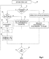
- the figure 4 is a block diagram illustrating the realization of an atomic data processing (block 30, ATOMIC PROCESS) on data contained in a page Pi of the region 22.
- steps 33 to 35 are performed if test 32 is executed after operation 33).
- At least one PCj page of the region 24 is deleted (block 36) in order to reuse it.
- block 36 we begin by erasing (block 36, ERASE P (B7MD (PCj))) a page P of the main region whose updated content is stored in region 22 by identifying the corresponding page Pi through the field B7MD of the PC page which contains the address of the corresponding page Pi. Then, the content of this page PCj in the main region 22 in the page Pi just deleted is transferred (block 36, PCj -> P (B7MD (PCj)) Finally, one erases (block 36, ERASE PCj ) the page PCj of the region 24 which can then be used again.
- step 34 (case shown) or step 34.
- step 35 is executed, it is tested whether the atomic operation is complete (block 37, AP END?). If yes (output Y of block 37), the processing stops (END). If not, return to step 31.
- step 36 all the PCj pages of the region 24 are deleted (block 36) in order to reuse them.
- block 36 ERASE P (B7MD (PCj))
- all the pages P of the main region whose updated content is stored in region 22 by identifying the corresponding pages Pi using the fields B7MD PCj pages which contain the addresses of the corresponding pages Pi.
- the contents of all these pages PCj in the main region 22 are transferred (block 36, PCj -> P (B7MD (PCj)) to the pages Pi which have just been erased
- one erases (block 36, ERASE PCj) all PCj pages of region 24.
- the cache region is then empty to be used sequentially again.
- the field B7MD (Pi) is not empty (output N of block 31) and indicates the address of a page PCj in region 24, it means that the data B0 to B6 of the page Pi are not valid (or are not stable data).
- the operation is then performed on the content of the PCj page (block 38, OPERATION ON PC (B7MD (Pi)) identified by the field B7MD of the page Pi.
- the result of the operation must be stored in a file. page Pi.
- the flag F0 is activated when starting the operation on the data, that is to say at the start of step 33 or 38, the flags F1 and F2 are also written at the start of step 33 or 38 to indicate the nature of the operation, and the flag F3 is activated before the test 37 to indicate the end of the operation.
- the described embodiment takes advantage of the difference in duration between the programming time and the erasure time.
- the operation of erasing a page is relatively long (typically of the order of a few milliseconds) compared to an operation programming a byte (typically of the order of ten microseconds).
- page size depends on the application and the maximum size needed to store a transaction.
- An advantage of the embodiments that have been described is that they improve the management of a flash memory for the processing of operations that must comply with an atomicity criterion.
Landscapes
- Engineering & Computer Science (AREA)
- Theoretical Computer Science (AREA)
- Physics & Mathematics (AREA)
- General Engineering & Computer Science (AREA)
- General Physics & Mathematics (AREA)
- Software Systems (AREA)
- Computer Hardware Design (AREA)
- Human Computer Interaction (AREA)
- Computer Security & Cryptography (AREA)
- Mathematical Physics (AREA)
- Techniques For Improving Reliability Of Storages (AREA)
- Information Retrieval, Db Structures And Fs Structures Therefor (AREA)
Claims (8)
- Verfahren zur Datenspeicherung in einem nichtflüchtigen Speicher (2), wobei der nichtflüchtige Speicher unterteilt ist in:einen ersten Bereich (22), in dem jede Seite Felder aufweist, die geeignet sind, Daten zu enthalten, und ein Feld, das geeignet ist, Metadaten zu enthalten;einen zweiten Bereich (24), in dem jede Seite Felder aufweist, die geeignet sind, Daten zu enthalten, und ein Feld, das geeignet ist, Metadaten zu enthalten;einen dritten Bereich (26), der geeignet ist, um Indikatoren für den Fortschritt einer Operation in der ersten und zweiten Bereichen zu enthalten,wobei die Metadatenfelder der ersten und zweiten Bereiche jeweils geeignet sind, um während eines Vorgangs der Datenaktualisierung einer Seite des ersten Bereichs die Indizes einer Seite im zweiten Bereich und der Seite des ersten Bereichs zu enthalten.
- Verfahren nach Anspruch 1, wobei es vier Indikatoren gibt, die jeweils Folgendes anzeigen:den Beginn einer Operation (F0);die Art der Operation (F1);eine Bestätigung, dass der Indikator für die Art der Operation stabil ist (F2); unddas Ende der Operation (F3).
- Verfahren nach Anspruch 1 oder 2, wobei die Seiten des zweiten Bereichs sequentiell verwendet werden.
- Verfahren nach einem der Ansprüche 1 bis 3, wobei für jede Anforderung für den Zugriff auf eine Seite im Speicher das Verfahren gestartet wird durch Lesen des Metadatenfeldes der entsprechenden Seite (Pi) im ersten Bereich gestartet wird, um zu bestimmen, ob die Daten in dieser Seite oder in einer Seite des zweiten Bereichs (24) enthalten sind.
- Verfahren nach einem der Ansprüche 1 bis 4, wobei während einer atomaren Verarbeitung von Daten, die in einer Seite (Pi) des ersten Bereichs (22) enthalten sind, diese Seite entweder die Anfangsdaten oder die Enddaten enthält, wobei die Zwischendaten in einer Seite (PCj) des zweiten Bereichs (24) enthalten sind.
- Verfahren zur Verwaltung eines nichtflüchtigen Speichers, in dem Daten durch Anwendung des Verfahrens nach einem der Ansprüche 1 bis 5 gespeichert werden.
- Flash-Speicher, der gemäß dem Verfahren nach einem der Ansprüche 1 bis 6 programmiert ist.
- Elektronische Schaltung, aufweisend den Flash-Speicher (2) nach Anspruch 7.
Applications Claiming Priority (1)
| Application Number | Priority Date | Filing Date | Title |
|---|---|---|---|
| FR1563375A FR3046266A1 (fr) | 2015-12-28 | 2015-12-28 | Stockage dans une memoire flash |
Publications (2)
| Publication Number | Publication Date |
|---|---|
| EP3188024A1 EP3188024A1 (de) | 2017-07-05 |
| EP3188024B1 true EP3188024B1 (de) | 2019-10-09 |
Family
ID=55300712
Family Applications (1)
| Application Number | Title | Priority Date | Filing Date |
|---|---|---|---|
| EP16161613.1A Active EP3188024B1 (de) | 2015-12-28 | 2016-03-22 | Speicherung in einem flash-speicher |
Country Status (4)
| Country | Link |
|---|---|
| US (1) | US10089029B2 (de) |
| EP (1) | EP3188024B1 (de) |
| CN (1) | CN106919344B (de) |
| FR (1) | FR3046266A1 (de) |
Families Citing this family (1)
| Publication number | Priority date | Publication date | Assignee | Title |
|---|---|---|---|---|
| CN114428592B (zh) * | 2022-03-25 | 2022-06-03 | 北京得瑞领新科技有限公司 | Ssd硬盘的块信息存储方法和系统、ssd硬盘 |
Family Cites Families (9)
| Publication number | Priority date | Publication date | Assignee | Title |
|---|---|---|---|---|
| CN1936853B (zh) * | 2005-09-22 | 2010-05-05 | 康佳集团股份有限公司 | 嵌入式设备的数据掉电保护和修复方法 |
| FR2950463B1 (fr) * | 2009-09-21 | 2011-12-09 | St Microelectronics Rousset | Procede de lecture d'une memoire non volatile au moyen de metadonnees et d'une table de correspondance |
| CN101763295B (zh) * | 2009-12-28 | 2012-05-30 | 北京握奇数据系统有限公司 | 一种数据备份、备份项擦除及数据恢复方法和装置 |
| US9251058B2 (en) * | 2010-09-28 | 2016-02-02 | SanDisk Technologies, Inc. | Servicing non-block storage requests |
| US8799555B2 (en) * | 2011-04-14 | 2014-08-05 | Apple Inc. | Boot data storage schemes for electronic devices |
| US20130019053A1 (en) * | 2011-07-14 | 2013-01-17 | Vinay Ashok Somanache | Flash controller hardware architecture for flash devices |
| US8949508B2 (en) * | 2011-07-18 | 2015-02-03 | Apple Inc. | Non-volatile temporary data handling |
| KR20140007990A (ko) * | 2012-07-09 | 2014-01-21 | 삼성전자주식회사 | 불휘발성 램을 포함하는 사용자 장치 및 그것의 데이터 관리 방법 |
| CN102789427B (zh) * | 2012-07-17 | 2015-11-25 | 威盛电子股份有限公司 | 数据储存装置与其操作方法 |
-
2015
- 2015-12-28 FR FR1563375A patent/FR3046266A1/fr active Pending
-
2016
- 2016-03-22 EP EP16161613.1A patent/EP3188024B1/de active Active
- 2016-05-30 CN CN201610371612.0A patent/CN106919344B/zh active Active
- 2016-06-28 US US15/195,881 patent/US10089029B2/en active Active
Non-Patent Citations (1)
| Title |
|---|
| None * |
Also Published As
| Publication number | Publication date |
|---|---|
| CN106919344B (zh) | 2019-09-24 |
| EP3188024A1 (de) | 2017-07-05 |
| US10089029B2 (en) | 2018-10-02 |
| CN106919344A (zh) | 2017-07-04 |
| FR3046266A1 (fr) | 2017-06-30 |
| US20170185334A1 (en) | 2017-06-29 |
Similar Documents
| Publication | Publication Date | Title |
|---|---|---|
| FR2606909A1 (fr) | Systeme de traitement pour un appareil electronique portatif, tel qu'une carte a circuit integre | |
| FR2687816A1 (fr) | Procede de personnalisation d'une carte a puce. | |
| EP2940690B1 (de) | Bidirektionaler Zähler in einem Flash-Speicher | |
| EP0552077B1 (de) | Massenspeicherkarte für einen Mikrocomputer mit der Möglichkeit, interne Programme auszuführen | |
| JP4588223B2 (ja) | いくつかのアプリケーション・ファイルにおけるコマンドを管理するための方法及びこの方法を実施するためのマイクロチップカード | |
| FR2757664A1 (fr) | Terminal et procede d'autodiagnostic ou de supervision et objet portatif utilise dans un tel terminal ou procede | |
| EP3293637A1 (de) | Indexverwaltung in einem flash-speicher | |
| FR2600444A1 (fr) | Appareil electronique portatif, tel que carte a circuit integre, permettant de determiner des la premiere transmission la validite d'une chaine de donnees | |
| EP3188024B1 (de) | Speicherung in einem flash-speicher | |
| CN101218609B (zh) | 带有安全的数据处理的便携式数据载体 | |
| EP3246820A1 (de) | Verwaltung der speicherung in einem flash-speicher | |
| JP6999679B2 (ja) | データ消去方法および装置 | |
| EP3246819B1 (de) | Zähler in einem flash-speicher | |
| FR2689662A1 (fr) | Procédé de protection d'une carte à puce contre la perte d'information. | |
| EP2901291B1 (de) | Verfahren zur verwaltung der speicherressourcen einer sicherheitsvorrichtung, z. b. einer chipkarte, und sicherheitsvorrichtung zur durchführung des verfahrens | |
| EP3188032B1 (de) | Datenspeicherung in einem flash-speicher | |
| FR3012655A1 (fr) | Compteur en memoire flash | |
| WO1999000774A9 (fr) | Module de securite comportant des moyens de creation de liens entre des fichiers principaux et des fichiers auxiliaires | |
| FR3051575A1 (fr) | Gestion de l'effacement dans une memoire flash | |
| FR2600445A1 (fr) | Appareil electronique portatif, tel que carte a circuit integre, permettant d'effectuer rapidement un effacement de donnee | |
| CN119917117A (zh) | 一种动态数据的芯片烧录系统及方法 | |
| FR2830667A1 (fr) | Procede de determination d'une zone stable dans une memoire et dispositif de gestion d'une memoire associe | |
| EP3416087A1 (de) | Steuerung der atomarität in einem eeprom-speicher | |
| FR2799046A1 (fr) | Procede pour l'ecriture aleatoire de secteurs d'une taille inferieure a celle d'un bloc d'effacement dans une memoire effacable par bloc pour laquelle toute ecriture d'une donnee necessite l'effacement du bloc qui contient ladite donnee |
Legal Events
| Date | Code | Title | Description |
|---|---|---|---|
| PUAI | Public reference made under article 153(3) epc to a published international application that has entered the european phase |
Free format text: ORIGINAL CODE: 0009012 |
|
| STAA | Information on the status of an ep patent application or granted ep patent |
Free format text: STATUS: REQUEST FOR EXAMINATION WAS MADE |
|
| 17P | Request for examination filed |
Effective date: 20160322 |
|
| AK | Designated contracting states |
Kind code of ref document: A1 Designated state(s): AL AT BE BG CH CY CZ DE DK EE ES FI FR GB GR HR HU IE IS IT LI LT LU LV MC MK MT NL NO PL PT RO RS SE SI SK SM TR |
|
| AX | Request for extension of the european patent |
Extension state: BA ME |
|
| GRAP | Despatch of communication of intention to grant a patent |
Free format text: ORIGINAL CODE: EPIDOSNIGR1 |
|
| STAA | Information on the status of an ep patent application or granted ep patent |
Free format text: STATUS: GRANT OF PATENT IS INTENDED |
|
| INTG | Intention to grant announced |
Effective date: 20190625 |
|
| RIN1 | Information on inventor provided before grant (corrected) |
Inventor name: DOCQUIER, GUILLAUME Inventor name: VAN KEER, RONNY |
|
| GRAS | Grant fee paid |
Free format text: ORIGINAL CODE: EPIDOSNIGR3 |
|
| GRAA | (expected) grant |
Free format text: ORIGINAL CODE: 0009210 |
|
| STAA | Information on the status of an ep patent application or granted ep patent |
Free format text: STATUS: THE PATENT HAS BEEN GRANTED |
|
| AK | Designated contracting states |
Kind code of ref document: B1 Designated state(s): AL AT BE BG CH CY CZ DE DK EE ES FI FR GB GR HR HU IE IS IT LI LT LU LV MC MK MT NL NO PL PT RO RS SE SI SK SM TR |
|
| REG | Reference to a national code |
Ref country code: GB Ref legal event code: FG4D Free format text: NOT ENGLISH |
|
| REG | Reference to a national code |
Ref country code: CH Ref legal event code: EP |
|
| REG | Reference to a national code |
Ref country code: DE Ref legal event code: R096 Ref document number: 602016021953 Country of ref document: DE |
|
| REG | Reference to a national code |
Ref country code: IE Ref legal event code: FG4D Free format text: LANGUAGE OF EP DOCUMENT: FRENCH |
|
| REG | Reference to a national code |
Ref country code: AT Ref legal event code: REF Ref document number: 1189625 Country of ref document: AT Kind code of ref document: T Effective date: 20191115 |
|
| REG | Reference to a national code |
Ref country code: NL Ref legal event code: MP Effective date: 20191009 |
|
| REG | Reference to a national code |
Ref country code: LT Ref legal event code: MG4D |
|
| REG | Reference to a national code |
Ref country code: AT Ref legal event code: MK05 Ref document number: 1189625 Country of ref document: AT Kind code of ref document: T Effective date: 20191009 |
|
| PG25 | Lapsed in a contracting state [announced via postgrant information from national office to epo] |
Ref country code: NL Free format text: LAPSE BECAUSE OF FAILURE TO SUBMIT A TRANSLATION OF THE DESCRIPTION OR TO PAY THE FEE WITHIN THE PRESCRIBED TIME-LIMIT Effective date: 20191009 Ref country code: AT Free format text: LAPSE BECAUSE OF FAILURE TO SUBMIT A TRANSLATION OF THE DESCRIPTION OR TO PAY THE FEE WITHIN THE PRESCRIBED TIME-LIMIT Effective date: 20191009 Ref country code: LT Free format text: LAPSE BECAUSE OF FAILURE TO SUBMIT A TRANSLATION OF THE DESCRIPTION OR TO PAY THE FEE WITHIN THE PRESCRIBED TIME-LIMIT Effective date: 20191009 Ref country code: PL Free format text: LAPSE BECAUSE OF FAILURE TO SUBMIT A TRANSLATION OF THE DESCRIPTION OR TO PAY THE FEE WITHIN THE PRESCRIBED TIME-LIMIT Effective date: 20191009 Ref country code: PT Free format text: LAPSE BECAUSE OF FAILURE TO SUBMIT A TRANSLATION OF THE DESCRIPTION OR TO PAY THE FEE WITHIN THE PRESCRIBED TIME-LIMIT Effective date: 20200210 Ref country code: ES Free format text: LAPSE BECAUSE OF FAILURE TO SUBMIT A TRANSLATION OF THE DESCRIPTION OR TO PAY THE FEE WITHIN THE PRESCRIBED TIME-LIMIT Effective date: 20191009 Ref country code: GR Free format text: LAPSE BECAUSE OF FAILURE TO SUBMIT A TRANSLATION OF THE DESCRIPTION OR TO PAY THE FEE WITHIN THE PRESCRIBED TIME-LIMIT Effective date: 20200110 Ref country code: BG Free format text: LAPSE BECAUSE OF FAILURE TO SUBMIT A TRANSLATION OF THE DESCRIPTION OR TO PAY THE FEE WITHIN THE PRESCRIBED TIME-LIMIT Effective date: 20200109 Ref country code: NO Free format text: LAPSE BECAUSE OF FAILURE TO SUBMIT A TRANSLATION OF THE DESCRIPTION OR TO PAY THE FEE WITHIN THE PRESCRIBED TIME-LIMIT Effective date: 20200109 Ref country code: FI Free format text: LAPSE BECAUSE OF FAILURE TO SUBMIT A TRANSLATION OF THE DESCRIPTION OR TO PAY THE FEE WITHIN THE PRESCRIBED TIME-LIMIT Effective date: 20191009 Ref country code: LV Free format text: LAPSE BECAUSE OF FAILURE TO SUBMIT A TRANSLATION OF THE DESCRIPTION OR TO PAY THE FEE WITHIN THE PRESCRIBED TIME-LIMIT Effective date: 20191009 Ref country code: SE Free format text: LAPSE BECAUSE OF FAILURE TO SUBMIT A TRANSLATION OF THE DESCRIPTION OR TO PAY THE FEE WITHIN THE PRESCRIBED TIME-LIMIT Effective date: 20191009 |
|
| PG25 | Lapsed in a contracting state [announced via postgrant information from national office to epo] |
Ref country code: HR Free format text: LAPSE BECAUSE OF FAILURE TO SUBMIT A TRANSLATION OF THE DESCRIPTION OR TO PAY THE FEE WITHIN THE PRESCRIBED TIME-LIMIT Effective date: 20191009 Ref country code: RS Free format text: LAPSE BECAUSE OF FAILURE TO SUBMIT A TRANSLATION OF THE DESCRIPTION OR TO PAY THE FEE WITHIN THE PRESCRIBED TIME-LIMIT Effective date: 20191009 Ref country code: IS Free format text: LAPSE BECAUSE OF FAILURE TO SUBMIT A TRANSLATION OF THE DESCRIPTION OR TO PAY THE FEE WITHIN THE PRESCRIBED TIME-LIMIT Effective date: 20200224 |
|
| PG25 | Lapsed in a contracting state [announced via postgrant information from national office to epo] |
Ref country code: AL Free format text: LAPSE BECAUSE OF FAILURE TO SUBMIT A TRANSLATION OF THE DESCRIPTION OR TO PAY THE FEE WITHIN THE PRESCRIBED TIME-LIMIT Effective date: 20191009 |
|
| REG | Reference to a national code |
Ref country code: DE Ref legal event code: R097 Ref document number: 602016021953 Country of ref document: DE |
|
| PG2D | Information on lapse in contracting state deleted |
Ref country code: IS |
|
| PG25 | Lapsed in a contracting state [announced via postgrant information from national office to epo] |
Ref country code: CZ Free format text: LAPSE BECAUSE OF FAILURE TO SUBMIT A TRANSLATION OF THE DESCRIPTION OR TO PAY THE FEE WITHIN THE PRESCRIBED TIME-LIMIT Effective date: 20191009 Ref country code: EE Free format text: LAPSE BECAUSE OF FAILURE TO SUBMIT A TRANSLATION OF THE DESCRIPTION OR TO PAY THE FEE WITHIN THE PRESCRIBED TIME-LIMIT Effective date: 20191009 Ref country code: DK Free format text: LAPSE BECAUSE OF FAILURE TO SUBMIT A TRANSLATION OF THE DESCRIPTION OR TO PAY THE FEE WITHIN THE PRESCRIBED TIME-LIMIT Effective date: 20191009 Ref country code: RO Free format text: LAPSE BECAUSE OF FAILURE TO SUBMIT A TRANSLATION OF THE DESCRIPTION OR TO PAY THE FEE WITHIN THE PRESCRIBED TIME-LIMIT Effective date: 20191009 Ref country code: IS Free format text: LAPSE BECAUSE OF FAILURE TO SUBMIT A TRANSLATION OF THE DESCRIPTION OR TO PAY THE FEE WITHIN THE PRESCRIBED TIME-LIMIT Effective date: 20200209 |
|
| PLBE | No opposition filed within time limit |
Free format text: ORIGINAL CODE: 0009261 |
|
| STAA | Information on the status of an ep patent application or granted ep patent |
Free format text: STATUS: NO OPPOSITION FILED WITHIN TIME LIMIT |
|
| PG25 | Lapsed in a contracting state [announced via postgrant information from national office to epo] |
Ref country code: IT Free format text: LAPSE BECAUSE OF FAILURE TO SUBMIT A TRANSLATION OF THE DESCRIPTION OR TO PAY THE FEE WITHIN THE PRESCRIBED TIME-LIMIT Effective date: 20191009 Ref country code: SK Free format text: LAPSE BECAUSE OF FAILURE TO SUBMIT A TRANSLATION OF THE DESCRIPTION OR TO PAY THE FEE WITHIN THE PRESCRIBED TIME-LIMIT Effective date: 20191009 Ref country code: SM Free format text: LAPSE BECAUSE OF FAILURE TO SUBMIT A TRANSLATION OF THE DESCRIPTION OR TO PAY THE FEE WITHIN THE PRESCRIBED TIME-LIMIT Effective date: 20191009 |
|
| 26N | No opposition filed |
Effective date: 20200710 |
|
| PG25 | Lapsed in a contracting state [announced via postgrant information from national office to epo] |
Ref country code: MC Free format text: LAPSE BECAUSE OF FAILURE TO SUBMIT A TRANSLATION OF THE DESCRIPTION OR TO PAY THE FEE WITHIN THE PRESCRIBED TIME-LIMIT Effective date: 20191009 |
|
| REG | Reference to a national code |
Ref country code: CH Ref legal event code: PL |
|
| PG25 | Lapsed in a contracting state [announced via postgrant information from national office to epo] |
Ref country code: SI Free format text: LAPSE BECAUSE OF FAILURE TO SUBMIT A TRANSLATION OF THE DESCRIPTION OR TO PAY THE FEE WITHIN THE PRESCRIBED TIME-LIMIT Effective date: 20191009 |
|
| REG | Reference to a national code |
Ref country code: BE Ref legal event code: MM Effective date: 20200331 |
|
| PG25 | Lapsed in a contracting state [announced via postgrant information from national office to epo] |
Ref country code: LU Free format text: LAPSE BECAUSE OF NON-PAYMENT OF DUE FEES Effective date: 20200322 |
|
| PG25 | Lapsed in a contracting state [announced via postgrant information from national office to epo] |
Ref country code: FR Free format text: LAPSE BECAUSE OF NON-PAYMENT OF DUE FEES Effective date: 20200331 Ref country code: LI Free format text: LAPSE BECAUSE OF NON-PAYMENT OF DUE FEES Effective date: 20200331 Ref country code: CH Free format text: LAPSE BECAUSE OF NON-PAYMENT OF DUE FEES Effective date: 20200331 Ref country code: IE Free format text: LAPSE BECAUSE OF NON-PAYMENT OF DUE FEES Effective date: 20200322 |
|
| PG25 | Lapsed in a contracting state [announced via postgrant information from national office to epo] |
Ref country code: BE Free format text: LAPSE BECAUSE OF NON-PAYMENT OF DUE FEES Effective date: 20200331 |
|
| GBPC | Gb: european patent ceased through non-payment of renewal fee |
Effective date: 20200322 |
|
| PG25 | Lapsed in a contracting state [announced via postgrant information from national office to epo] |
Ref country code: GB Free format text: LAPSE BECAUSE OF NON-PAYMENT OF DUE FEES Effective date: 20200322 |
|
| PG25 | Lapsed in a contracting state [announced via postgrant information from national office to epo] |
Ref country code: TR Free format text: LAPSE BECAUSE OF FAILURE TO SUBMIT A TRANSLATION OF THE DESCRIPTION OR TO PAY THE FEE WITHIN THE PRESCRIBED TIME-LIMIT Effective date: 20191009 Ref country code: MT Free format text: LAPSE BECAUSE OF FAILURE TO SUBMIT A TRANSLATION OF THE DESCRIPTION OR TO PAY THE FEE WITHIN THE PRESCRIBED TIME-LIMIT Effective date: 20191009 Ref country code: CY Free format text: LAPSE BECAUSE OF FAILURE TO SUBMIT A TRANSLATION OF THE DESCRIPTION OR TO PAY THE FEE WITHIN THE PRESCRIBED TIME-LIMIT Effective date: 20191009 |
|
| PG25 | Lapsed in a contracting state [announced via postgrant information from national office to epo] |
Ref country code: MK Free format text: LAPSE BECAUSE OF FAILURE TO SUBMIT A TRANSLATION OF THE DESCRIPTION OR TO PAY THE FEE WITHIN THE PRESCRIBED TIME-LIMIT Effective date: 20191009 |
|
| REG | Reference to a national code |
Ref country code: DE Ref legal event code: R081 Ref document number: 602016021953 Country of ref document: DE Owner name: STMICROELECTRONICS INTERNATIONAL N.V., CH Free format text: FORMER OWNER: PROTON WORLD INTERNATIONAL N.V., DIEGEM, BE |
|
| PGFP | Annual fee paid to national office [announced via postgrant information from national office to epo] |
Ref country code: DE Payment date: 20250218 Year of fee payment: 10 |