EP3416087A1 - Steuerung der atomarität in einem eeprom-speicher - Google Patents
Steuerung der atomarität in einem eeprom-speicher Download PDFInfo
- Publication number
- EP3416087A1 EP3416087A1 EP18176712.0A EP18176712A EP3416087A1 EP 3416087 A1 EP3416087 A1 EP 3416087A1 EP 18176712 A EP18176712 A EP 18176712A EP 3416087 A1 EP3416087 A1 EP 3416087A1
- Authority
- EP
- European Patent Office
- Prior art keywords
- value
- data
- flag
- eeprom memory
- block
- Prior art date
- Legal status (The legal status is an assumption and is not a legal conclusion. Google has not performed a legal analysis and makes no representation as to the accuracy of the status listed.)
- Withdrawn
Links
Images


Classifications
-
- G—PHYSICS
- G06—COMPUTING; CALCULATING OR COUNTING
- G06F—ELECTRIC DIGITAL DATA PROCESSING
- G06F11/00—Error detection; Error correction; Monitoring
- G06F11/07—Responding to the occurrence of a fault, e.g. fault tolerance
- G06F11/14—Error detection or correction of the data by redundancy in operation
- G06F11/1402—Saving, restoring, recovering or retrying
- G06F11/1415—Saving, restoring, recovering or retrying at system level
- G06F11/1441—Resetting or repowering
-
- G—PHYSICS
- G11—INFORMATION STORAGE
- G11C—STATIC STORES
- G11C16/00—Erasable programmable read-only memories
- G11C16/02—Erasable programmable read-only memories electrically programmable
- G11C16/06—Auxiliary circuits, e.g. for writing into memory
- G11C16/10—Programming or data input circuits
- G11C16/20—Initialising; Data preset; Chip identification
-
- G—PHYSICS
- G06—COMPUTING; CALCULATING OR COUNTING
- G06F—ELECTRIC DIGITAL DATA PROCESSING
- G06F21/00—Security arrangements for protecting computers, components thereof, programs or data against unauthorised activity
- G06F21/70—Protecting specific internal or peripheral components, in which the protection of a component leads to protection of the entire computer
- G06F21/78—Protecting specific internal or peripheral components, in which the protection of a component leads to protection of the entire computer to assure secure storage of data
- G06F21/79—Protecting specific internal or peripheral components, in which the protection of a component leads to protection of the entire computer to assure secure storage of data in semiconductor storage media, e.g. directly-addressable memories
-
- G—PHYSICS
- G06—COMPUTING; CALCULATING OR COUNTING
- G06F—ELECTRIC DIGITAL DATA PROCESSING
- G06F11/00—Error detection; Error correction; Monitoring
- G06F11/07—Responding to the occurrence of a fault, e.g. fault tolerance
- G06F11/08—Error detection or correction by redundancy in data representation, e.g. by using checking codes
- G06F11/10—Adding special bits or symbols to the coded information, e.g. parity check, casting out 9's or 11's
- G06F11/1004—Adding special bits or symbols to the coded information, e.g. parity check, casting out 9's or 11's to protect a block of data words, e.g. CRC or checksum
-
- G—PHYSICS
- G06—COMPUTING; CALCULATING OR COUNTING
- G06F—ELECTRIC DIGITAL DATA PROCESSING
- G06F11/00—Error detection; Error correction; Monitoring
- G06F11/07—Responding to the occurrence of a fault, e.g. fault tolerance
- G06F11/14—Error detection or correction of the data by redundancy in operation
- G06F11/1402—Saving, restoring, recovering or retrying
- G06F11/1405—Saving, restoring, recovering or retrying at machine instruction level
- G06F11/141—Saving, restoring, recovering or retrying at machine instruction level for bus or memory accesses
-
- G—PHYSICS
- G11—INFORMATION STORAGE
- G11C—STATIC STORES
- G11C16/00—Erasable programmable read-only memories
- G11C16/02—Erasable programmable read-only memories electrically programmable
- G11C16/04—Erasable programmable read-only memories electrically programmable using variable threshold transistors, e.g. FAMOS
- G11C16/0408—Erasable programmable read-only memories electrically programmable using variable threshold transistors, e.g. FAMOS comprising cells containing floating gate transistors
- G11C16/0433—Erasable programmable read-only memories electrically programmable using variable threshold transistors, e.g. FAMOS comprising cells containing floating gate transistors comprising cells containing a single floating gate transistor and one or more separate select transistors
-
- G—PHYSICS
- G11—INFORMATION STORAGE
- G11C—STATIC STORES
- G11C16/00—Erasable programmable read-only memories
- G11C16/02—Erasable programmable read-only memories electrically programmable
- G11C16/06—Auxiliary circuits, e.g. for writing into memory
- G11C16/10—Programming or data input circuits
- G11C16/102—External programming circuits, e.g. EPROM programmers; In-circuit programming or reprogramming; EPROM emulators
- G11C16/105—Circuits or methods for updating contents of nonvolatile memory, especially with 'security' features to ensure reliable replacement, i.e. preventing that old data is lost before new data is reliably written
-
- G—PHYSICS
- G11—INFORMATION STORAGE
- G11C—STATIC STORES
- G11C16/00—Erasable programmable read-only memories
- G11C16/02—Erasable programmable read-only memories electrically programmable
- G11C16/06—Auxiliary circuits, e.g. for writing into memory
- G11C16/10—Programming or data input circuits
- G11C16/14—Circuits for erasing electrically, e.g. erase voltage switching circuits
-
- G—PHYSICS
- G11—INFORMATION STORAGE
- G11C—STATIC STORES
- G11C16/00—Erasable programmable read-only memories
- G11C16/02—Erasable programmable read-only memories electrically programmable
- G11C16/06—Auxiliary circuits, e.g. for writing into memory
- G11C16/26—Sensing or reading circuits; Data output circuits
-
- G—PHYSICS
- G11—INFORMATION STORAGE
- G11C—STATIC STORES
- G11C16/00—Erasable programmable read-only memories
- G11C16/02—Erasable programmable read-only memories electrically programmable
- G11C16/06—Auxiliary circuits, e.g. for writing into memory
- G11C16/34—Determination of programming status, e.g. threshold voltage, overprogramming or underprogramming, retention
- G11C16/3436—Arrangements for verifying correct programming or erasure
- G11C16/3454—Arrangements for verifying correct programming or for detecting overprogrammed cells
-
- G—PHYSICS
- G06—COMPUTING; CALCULATING OR COUNTING
- G06F—ELECTRIC DIGITAL DATA PROCESSING
- G06F2201/00—Indexing scheme relating to error detection, to error correction, and to monitoring
- G06F2201/82—Solving problems relating to consistency
-
- G—PHYSICS
- G11—INFORMATION STORAGE
- G11C—STATIC STORES
- G11C2211/00—Indexing scheme relating to digital stores characterized by the use of particular electric or magnetic storage elements; Storage elements therefor
- G11C2211/56—Indexing scheme relating to G11C11/56 and sub-groups for features not covered by these groups
- G11C2211/564—Miscellaneous aspects
- G11C2211/5646—Multilevel memory with flag bits, e.g. for showing that a "first page" of a word line is programmed but not a "second page"
Definitions
- the present description generally relates to electronic circuits and, more particularly, circuits using a rewritable non-volatile memory.
- the present description aims more particularly the atomicity management in an EEPROM memory.
- EEPROM memories are used, in particular in microcontrollers, for nonvolatile storage of information.
- the atomicity of a transaction is to ensure that data stored in memory has an exploitable state and integrity. This is to ensure that data in non-volatile memory has a stable state (the state before the transaction or the state after the transaction concerned).
- Transaction Atomicity Management is particularly used in applications where an interruption in circuit power or the occurrence of an accidental or deliberate disruption may result in the storage of data in a state rendering it unusable by remain vulnerable in terms of confidentiality or integrity.
- an interruption in circuit power or the occurrence of an accidental or deliberate disruption may result in the storage of data in a state rendering it unusable by remain vulnerable in terms of confidentiality or integrity.
- the equivalent of the tearing out corresponds to a power failure of the circuit.
- the document EP 0 630 027 discloses a method for securing the writes of sensitive data in the EEPROM data storage memory of a memory card, and a memory card for carrying out this method.
- the document WO 89/10618 discloses a method for preventing data being written to a non-volatile memory from being corrupted by a power failure.
- EP 2,299,363 discloses a method of leveling wear in a non-volatile memory.
- One embodiment overcomes all or some of the disadvantages of known techniques.
- the value of the data is returned only if the value of the first flag corresponds to the second value.
- the data is erased in the EEPROM memory.
- the value of the two flags is updated with the first value in the EEPROM memory.
- the first value corresponds to an erasure.
- the first and second flags are updated and read successively.
- the values of the first and second flags are updated with their respective second value in the EEPROM memory.
- One embodiment relates to an electronic circuit comprising an EEPROM memory, and a processor adapted to the implementation of the method for verifying the atomic character of a data updating operation in the EEPROM memory.
- the figure 1 represents very schematically and in the form of blocks, an embodiment of an electronic circuit 1 of the type to which apply, by way of example, the embodiments that will be described.
- the circuit 1 also integrates a contactless communication circuit 16 (CLF - ContactLess Front-end), Near Field Communication (NFC) type.
- CLF contactless communication circuit 16
- NFC Near Field Communication
- circuit 1 can integrate other functions, symbolized by a block 17 (FCT), depending on the application, for example, a crypto-processor, other interfaces, other memories, etc.
- FCT a block 17
- the storage of data in the EEPROM memory must only be considered valid once the transaction is over and the data are said to be stable.
- the atomicity management methods activate a data processing indicator when it is extracted from the non-volatile memory, and then organize the storage of the updated data once the processing is completed, the indicator processing then changing state. Atomicity can concern a larger or smaller amount of data depending on the nature of the transaction.
- the atomic character of the transactions is particularly important in the case of bank type transactions (payment for example) where it is necessary to ensure that the information stored in the EEPROM, for example the balance an electronic purse or purchase authorization, or the identifier validating a transaction, is stored reliably.
- atomic temporary storage spaces (Buffer) are used which are updated in non-volatile memory with the initial and then final information for transfer to the main non-volatile memory.
- the management of the atomicity of the transactions in a circuit equipped with an EEPROM memory is generally carried out on two states, that is to say that the atomicity verification algorithms are capable of restoring a datum of the memory in a stable state, corresponding to the initial state or the final state.
- the implementation of these security requires an important place in memory and complex recovery algorithms that are not always justified.
- the multiple writes of a data adversely affect memory endurance and consumption.
- Predicting an indeterminate or "unreliable” state simplifies the constraints in terms of the execution time of the processes and reduces the number of required updates of the memory.
- This aspect is particularly important in the case of an EEPROM memory whose endurance (lifetime) and consumption are highly dependent on the number of writes. This problem does not necessarily arise for other types of memories that consume less in writes operations (an EEPROM type memory requires a write voltage of more than ten volts) or whose endurance is less critical.
- two flags or atomicity indicators of one or more bits for example one byte
- the size of which is independent of the size of the data to be protected are provided.
- the figure 2 represents schematically and in block form, the steps of updating a data by implementing an example of atomicity management method.
- the management of the atomicity requires a word (for example a bit or a byte) serving as flag, or witness, of atomicity which must be stored in non-volatile memory.
- the data word d to be updated (block 23, ERASE d) is erased.
- the new value D of the word d is then written (block 24, d ⁇ - D) in its memory location.
- a known value for example M is written (block 25, f ⁇ - M), different from the initialization value used in step 22 in the flag word f.
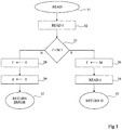
- the figure 3 represents, schematically and in block form, the steps of an exemplary method of reading a written data by implementing the atomicity management method of the figure 2 .
- step 34 is preceded by a step (block 36, f ⁇ - M) confirming the value M in the flag f.
- step 36 may take place after step 34.
- step 37 is preceded by steps (block 38, f ⁇ - 0 and block 39, d ⁇ - 0) of confirmation of the initialization value (0) of the flag and of the erasure of the datum d .
- step 38 is performed before step 39.
- step 39 is performed before step 38, a situation could be found in which an unstable (unreliable) f-value would direct (test 33) the algorithm a first time to steps 39 and 38.
- Step 38 of confirming the value of the flag f to the value 0 serves to avoid a false first reading. Indeed, in the absence of confirmation, one could meet the situation of an unstable flag f which would be read alternately with the value M and with a value different from M. The confirmation serves thus to avoid that two successive readings do not give different results.
- the erasure step 39 of the data item d ensures that a subsequent reading provides something unusable.
- the figure 4 represents schematically and in block form, the steps of updating a data by implementing an embodiment of an atomicity management method.
- each update (block 41, UPDATE d) of a data whose value D is stored in the EEPROM memory one starts (block 42, f1 ⁇ - 0) by initializing a first word f1 serving as a flag in memory non-volatile to a known value (for example 0) and (block 42 ', f2 ⁇ -0) a second word f2 also serving as flag in non-volatile memory at a known value (for example 0).
- the data word d to be updated (block 43, d ⁇ - 0) is erased.
- the new value D of the word d is then written (block 44, d ⁇ - D) in its memory location.
- the figure 5 represents, schematically and in block form, the steps of an embodiment of a method of reading a written data by implementing the atomicity management method of the figure 4 .
- step 57 is preceded by steps (block 58, f1 ⁇ - 0, block 58 ', f2 ⁇ - 0, block 59, d ⁇ - 0) of confirmation of the initialization value (0) of the flags f1 and f2 and deletion of the data d.
- the flag confirmation steps (58 and 58 ') are preferably performed at the initialization value (0) before erasing (59) the data to detect a double interruption and thus to avoid validating, during a second reading, a false first reading.
- the erasure step 59 of the data item d ensures that a subsequent reading provides something unusable.
- test 53 ' is positive (output Y of the block 53'), so that the two tests 53 and 53 'are successively positive, it means that the data d is stable. It is then possible to read (block 54, READ d) the data item d and return the value D (block 55, RETURN D). A difference compared to the embodiment of the figure 3 is that the data d is read without the need to confirm the values of the flags.
- Steps (block 56, f1 ⁇ - M1, block 56 ', f2 ⁇ - M2) of confirmation of the values M1 and M2 in the respective flags f1 and f2 are then carried out before reading the data item d (block 54) and return the value D (block 55).
- steps 52, 52 ' can be reversed. On the other hand, it is possible to begin by performing steps 52 and 53 and then performing steps 52 'and 53' in the case of a positive test. In addition, step 54 can take place before steps 56 and 56 'or be interposed therebetween.
- the values M1 and M2 may be identical or different from each other.
- the determined or known value (s) (M1 and M2) required to confirm the atomicity may be any, provided they are different from the initialization value.
- Flags f1 and f2 do not need to be large. For example, one bit is enough. However, according to a preferred embodiment, a size corresponding to the writing granularity of the EEPROM memory, for example a byte, will be chosen.
- One advantage is that it increases the reliability of the flags at no additional cost for writing. For example, it is possible to use certain bits of the byte to associate, with the flag or flags, an error correction code. In the embodiment of figures 4 and 5 , it can be expected that each flag is a half-byte to save a write step (confirmation) at each reading.
- the flags f1 and f2 can be stored in the EEPROM independently of the data d, that is to say not necessarily in the same memory page.
- An advantage of the embodiments described is that they avoid having to duplicate the initial value in order to recover it as is the case in a two-state process. This saves a writing in nonvolatile memory of the data, which represents a gain in terms of energy and endurance of the EEPROM, especially for data of significant size.
- the atomicity verification method is not necessarily implemented for all the data stored in the EEPROM. Preferably, it is implemented only for the data for which it is desired to ensure that the data state is stable or not at each reading.
- the steps 23 (or 43) and 24 (or 44), corresponding to the steps of erasing and writing the data, may not be successive and be separated from processing steps or operations related to the algorithm exploiting this data. These steps will be protected in the sense that in case of power failure after the erase step, the data will be considered unstable until the next writing and above all will be unusable because cleared.
Applications Claiming Priority (1)
| Application Number | Priority Date | Filing Date | Title |
|---|---|---|---|
| FR1755351A FR3067831A1 (fr) | 2017-06-14 | 2017-06-14 | Gestion d'atomicite dans une memoire eeprom |
Publications (1)
| Publication Number | Publication Date |
|---|---|
| EP3416087A1 true EP3416087A1 (de) | 2018-12-19 |
Family
ID=59930490
Family Applications (1)
| Application Number | Title | Priority Date | Filing Date |
|---|---|---|---|
| EP18176712.0A Withdrawn EP3416087A1 (de) | 2017-06-14 | 2018-06-08 | Steuerung der atomarität in einem eeprom-speicher |
Country Status (4)
| Country | Link |
|---|---|
| US (1) | US10714189B2 (de) |
| EP (1) | EP3416087A1 (de) |
| CN (1) | CN109086633A (de) |
| FR (1) | FR3067831A1 (de) |
Citations (3)
| Publication number | Priority date | Publication date | Assignee | Title |
|---|---|---|---|---|
| WO1989010618A1 (en) * | 1988-04-29 | 1989-11-02 | Scientific Atlanta, Inc. | Dynamic double buffer |
| EP0630027A1 (de) * | 1993-05-26 | 1994-12-21 | SOLAIC (société anonyme) | Verfahren zum Abspeichern und Sichern von empfindlicher Daten in eine EEPROM Speicherkarte und entsprechende Speicherkarte. |
| EP2299363A1 (de) * | 2009-09-21 | 2011-03-23 | STMicroelectronics (Rousset) SAS | Verfahren zur Nivellierung des Verschleißes in einem nichtflüchtigen Speicher |
Family Cites Families (2)
| Publication number | Priority date | Publication date | Assignee | Title |
|---|---|---|---|---|
| CN103914393B (zh) * | 2014-04-11 | 2017-01-11 | 四川华拓光通信股份有限公司 | 一种基于mcu的flash不丢失更新存储方法 |
| CN104810055B (zh) * | 2015-05-08 | 2018-09-07 | 京东方科技集团股份有限公司 | Flash芯片读写控制电路和方法、AMOLED应用电路 |
-
2017
- 2017-06-14 FR FR1755351A patent/FR3067831A1/fr not_active Withdrawn
-
2018
- 2018-05-31 CN CN201810553339.2A patent/CN109086633A/zh active Pending
- 2018-06-08 EP EP18176712.0A patent/EP3416087A1/de not_active Withdrawn
- 2018-06-13 US US16/007,941 patent/US10714189B2/en active Active
Patent Citations (3)
| Publication number | Priority date | Publication date | Assignee | Title |
|---|---|---|---|---|
| WO1989010618A1 (en) * | 1988-04-29 | 1989-11-02 | Scientific Atlanta, Inc. | Dynamic double buffer |
| EP0630027A1 (de) * | 1993-05-26 | 1994-12-21 | SOLAIC (société anonyme) | Verfahren zum Abspeichern und Sichern von empfindlicher Daten in eine EEPROM Speicherkarte und entsprechende Speicherkarte. |
| EP2299363A1 (de) * | 2009-09-21 | 2011-03-23 | STMicroelectronics (Rousset) SAS | Verfahren zur Nivellierung des Verschleißes in einem nichtflüchtigen Speicher |
Also Published As
| Publication number | Publication date |
|---|---|
| FR3067831A1 (fr) | 2018-12-21 |
| US20180366200A1 (en) | 2018-12-20 |
| CN109086633A (zh) | 2018-12-25 |
| US10714189B2 (en) | 2020-07-14 |
Similar Documents
| Publication | Publication Date | Title |
|---|---|---|
| EP2940690B1 (de) | Bidirektionaler Zähler in einem Flash-Speicher | |
| EP0606029B1 (de) | IC Karte mit alterunggeschützten Daten und Programmen | |
| FR2810152A1 (fr) | Memoire eeprom securisee comprenant un circuit de correction d'erreur | |
| EP3293637A1 (de) | Indexverwaltung in einem flash-speicher | |
| FR2982406A1 (fr) | Memoire securisee qui evite la degradation de donnees | |
| EP0769742B1 (de) | Elektronisches Bauelement mit einem elektrisch löschbaren und nichtflüchtigen Speicher | |
| FR2856490A1 (fr) | Procede d'ecriture, de mise a jour et d'allocation memoire applique a l'ecriture de fichiers sur un support memoire tel qu'une carte a puce | |
| EP2369521A1 (de) | Schutz von Registern gegen einseitige Störungen | |
| EP3246820A1 (de) | Verwaltung der speicherung in einem flash-speicher | |
| EP3416087A1 (de) | Steuerung der atomarität in einem eeprom-speicher | |
| EP3246819B1 (de) | Zähler in einem flash-speicher | |
| FR2689662A1 (fr) | Procédé de protection d'une carte à puce contre la perte d'information. | |
| EP3522020B1 (de) | Management eines nicht-flüchtigen speichers | |
| WO2007090857A1 (fr) | Procede de mise a jour securisee de memoire non volatile | |
| FR3012655A1 (fr) | Compteur en memoire flash | |
| EP1508901B1 (de) | Speicherschaltung mit nichtflüchtigem Identifikationsspeicher und zugehöriges Verfahren | |
| FR2818426A1 (fr) | Dispositif et procede de securisation de zones de donnees dans une carte a puce | |
| EP2383746B1 (de) | Schreib- und Leseverfahren in einem Atomizitätsspeicher | |
| EP3188032B1 (de) | Datenspeicherung in einem flash-speicher | |
| FR3051575A1 (fr) | Gestion de l'effacement dans une memoire flash | |
| FR2915828A1 (fr) | Memoire non volatile a secteurs auxiliaires tournants | |
| EP3188024A1 (de) | Speicherung in einem flash-speicher | |
| WO2004055741A2 (fr) | Procédé sécurisé de modification de données enregistrées dans une carte à mémoire | |
| FR2830667A1 (fr) | Procede de determination d'une zone stable dans une memoire et dispositif de gestion d'une memoire associe | |
| FR3103925A1 (fr) | Procédé de modification d'une valeur de compteur d'un compteur d'une puce électronique |
Legal Events
| Date | Code | Title | Description |
|---|---|---|---|
| PUAI | Public reference made under article 153(3) epc to a published international application that has entered the european phase |
Free format text: ORIGINAL CODE: 0009012 |
|
| STAA | Information on the status of an ep patent application or granted ep patent |
Free format text: STATUS: REQUEST FOR EXAMINATION WAS MADE |
|
| 17P | Request for examination filed |
Effective date: 20180608 |
|
| AK | Designated contracting states |
Kind code of ref document: A1 Designated state(s): AL AT BE BG CH CY CZ DE DK EE ES FI FR GB GR HR HU IE IS IT LI LT LU LV MC MK MT NL NO PL PT RO RS SE SI SK SM TR |
|
| AX | Request for extension of the european patent |
Extension state: BA ME |
|
| STAA | Information on the status of an ep patent application or granted ep patent |
Free format text: STATUS: EXAMINATION IS IN PROGRESS |
|
| 17Q | First examination report despatched |
Effective date: 20191211 |
|
| STAA | Information on the status of an ep patent application or granted ep patent |
Free format text: STATUS: THE APPLICATION IS DEEMED TO BE WITHDRAWN |
|
| 18D | Application deemed to be withdrawn |
Effective date: 20200603 |