EP3186650B1 - Verfahren zur bestimmung eines innenwiderstands eines elektrischen energiespeichers - Google Patents
Verfahren zur bestimmung eines innenwiderstands eines elektrischen energiespeichers Download PDFInfo
- Publication number
- EP3186650B1 EP3186650B1 EP15734174.4A EP15734174A EP3186650B1 EP 3186650 B1 EP3186650 B1 EP 3186650B1 EP 15734174 A EP15734174 A EP 15734174A EP 3186650 B1 EP3186650 B1 EP 3186650B1
- Authority
- EP
- European Patent Office
- Prior art keywords
- method step
- current
- value
- values
- voltage
- Prior art date
- Legal status (The legal status is an assumption and is not a legal conclusion. Google has not performed a legal analysis and makes no representation as to the accuracy of the status listed.)
- Active
Links
Images



Classifications
-
- G—PHYSICS
- G01—MEASURING; TESTING
- G01R—MEASURING ELECTRIC VARIABLES; MEASURING MAGNETIC VARIABLES
- G01R31/00—Arrangements for testing electric properties; Arrangements for locating electric faults; Arrangements for electrical testing characterised by what is being tested not provided for elsewhere
- G01R31/36—Arrangements for testing, measuring or monitoring the electrical condition of accumulators or electric batteries, e.g. capacity or state of charge [SoC]
- G01R31/389—Measuring internal impedance, internal conductance or related variables
-
- G—PHYSICS
- G01—MEASURING; TESTING
- G01R—MEASURING ELECTRIC VARIABLES; MEASURING MAGNETIC VARIABLES
- G01R31/00—Arrangements for testing electric properties; Arrangements for locating electric faults; Arrangements for electrical testing characterised by what is being tested not provided for elsewhere
- G01R31/36—Arrangements for testing, measuring or monitoring the electrical condition of accumulators or electric batteries, e.g. capacity or state of charge [SoC]
- G01R31/3644—Constructional arrangements
- G01R31/3648—Constructional arrangements comprising digital calculation means, e.g. for performing an algorithm
-
- G—PHYSICS
- G01—MEASURING; TESTING
- G01R—MEASURING ELECTRIC VARIABLES; MEASURING MAGNETIC VARIABLES
- G01R31/00—Arrangements for testing electric properties; Arrangements for locating electric faults; Arrangements for electrical testing characterised by what is being tested not provided for elsewhere
- G01R31/36—Arrangements for testing, measuring or monitoring the electrical condition of accumulators or electric batteries, e.g. capacity or state of charge [SoC]
- G01R31/382—Arrangements for monitoring battery or accumulator variables, e.g. SoC
- G01R31/3842—Arrangements for monitoring battery or accumulator variables, e.g. SoC combining voltage and current measurements
-
- H—ELECTRICITY
- H01—ELECTRIC ELEMENTS
- H01M—PROCESSES OR MEANS, e.g. BATTERIES, FOR THE DIRECT CONVERSION OF CHEMICAL ENERGY INTO ELECTRICAL ENERGY
- H01M10/00—Secondary cells; Manufacture thereof
- H01M10/42—Methods or arrangements for servicing or maintenance of secondary cells or secondary half-cells
- H01M10/48—Accumulators combined with arrangements for measuring, testing or indicating the condition of cells, e.g. the level or density of the electrolyte
-
- Y—GENERAL TAGGING OF NEW TECHNOLOGICAL DEVELOPMENTS; GENERAL TAGGING OF CROSS-SECTIONAL TECHNOLOGIES SPANNING OVER SEVERAL SECTIONS OF THE IPC; TECHNICAL SUBJECTS COVERED BY FORMER USPC CROSS-REFERENCE ART COLLECTIONS [XRACs] AND DIGESTS
- Y02—TECHNOLOGIES OR APPLICATIONS FOR MITIGATION OR ADAPTATION AGAINST CLIMATE CHANGE
- Y02E—REDUCTION OF GREENHOUSE GAS [GHG] EMISSIONS, RELATED TO ENERGY GENERATION, TRANSMISSION OR DISTRIBUTION
- Y02E60/00—Enabling technologies; Technologies with a potential or indirect contribution to GHG emissions mitigation
- Y02E60/10—Energy storage using batteries
Definitions
- the internal resistance of an energy storage device can be determined in various ways. In the vehicle sector, the differential resistance, the zero-phase resistance or the ohmic resistance are usually calculated and from this the internal resistance is determined. A method for determining the internal resistance by means of the calculation of the differential resistance is in the published patent application WO 2006037694 A1 disclosed.
- the method requires only a small amount of computation compared to other methods for determining the internal resistance, for example, a method by means of spectral method in which the internal resistance is determined by discrete Fourier transformation.
- the method is also optimized for use in an embedded system, such as an electrical system Battery sensor, and can be used for both active and passive determination of internal resistance.
- An active determination here refers to the excitation of the electrical energy store with a controlled AC voltage at specific frequencies.
- the main advantage is that the internal resistance can be calculated continuously and independently of the mains voltage.
- the active provision requires complex hardware with power electronics and also loads the battery.
- a passive determination refers to the excitation of the electrical energy storage by a mains voltage of an alternator or by a consumer.
- the hardware requirements are thereby lower, since only a measurement of the current and the voltage of the energy storage are necessary. This can be implemented, for example, by a shunt or a Hall sensor.
- this passive determination does not directly control the excitation of the energy store, the internal resistance is not updated if the calculation requirements are not met. Further, by changing the threshold current value, the accuracy of the determination of the internal resistance can be adjusted.
- An advantageous embodiment of the method according to the invention provides that a further method step f takes place between the method step a and the method step e, in which the validity of the digital voltage values and the digital current values is checked.
- the digital voltage values and digital current values are valid if the method step a was successfully performed.
- the method is ended. It is advantageous here that the method is continued only with valid, ie error-free, measured values. On the one hand, the calculation effort can be reduced in the case of erroneous measured values, and on the other hand it can be avoided that a faulty zero-phase resistance is provided as internal resistance.
- a further advantageous embodiment of the method according to the invention provides that the current peak value or even the peak voltage value are determined by means of one, in particular three-element, first in-first out (FIFO) principle. It is advantageous here that the FIFO principle represents a simple means to a Peak value to be determined from several values. As a result, the computing power required for this process step is kept low.
- FIFO first in-first out
- the zero-phase resistance is considered plausible if it is between a theoretical minimum limit and a theoretical maximum limit of the expected internal resistance. If this is not the case, the procedure is terminated.
- the calculated zero-phase resistance is only provided in step e as internal resistance, if it is classified as plausible. As a result, the provision of a faulty zero-phase resistance as an internal resistance can be avoided.
- the calculation of the zero-phase resistance in method step d takes place by forming a quotient of voltage peak value and current peak value. It is advantageous here that this represents a simple possibility for calculating the zero-phase resistance and thus requires only a small computing capacity.
- An advantageous embodiment of the method according to the invention provides that between method step d and method step e a further method step h takes place, in which the calculated zero-phase resistance is low-pass filtered, in particular by means of a PT1 element.
- the advantage here is that the standard deviation can be reduced by the filtering, which occurs for example due to measurement noise.
- a further advantageous embodiment of the method according to the invention provides that the calculation of the zero-phase resistance in method step d takes place by forming a quotient of the quadratic mean of the voltage peak values relative to the quadratic mean of the current peak values. It is advantageous here that the accuracy in the calculation of the zero-phase resistance is further increased by this method of calculation.
- Fig. 1 shows a first embodiment of a method according to the invention for determining the internal resistance of an electrical energy storage device.
- the method begins at start S.
- a method step a an analog voltage signal U analog and an analog current signal I analog to the electrical energy store are converted into digital voltage values U and digital current values I.
- This analog / digital conversion takes place in method step a by means of a first sub-step a1 and a second sub-step a2.
- the analog voltage signal U is analog- low-pass filtered and the analog current signal I analog , this being done for example by means of an analog low-pass filter.
- the low-pass-filtered analog voltage signal U is sampled analogously and the low-pass filtered analog current signal I is sampled analogously in order to obtain digital voltage values U and digital current values I.
- the sampling for the analog voltage signal U is analog and the analog current signal I analog synchronous and provided that a sampling frequency f Tast is at least twice as large as a maximum zero phase frequency f zp, max .
- the low-pass filtering serves to ensure that the bandwidth of the signal to be sampled satisfies the sampling rate. Furthermore, the prerequisite for the sampling frequency fTast satisfies the Nyquist-Shannon sampling theorem.
- the digital voltage values U and the digital current values I are filtered in a subsequent method step b.
- the filtering is done here by means of a bandpass filter, which filters around a zero-phase frequency f zp around. at of this zero-phase frequency f zp , the impedance angle is approximately zero.
- the zero-phase frequency f zp depends , for example, on the type of energy storage, the temperature and the state of charge. For lead-acid batteries, the zero-phase frequency f zp typically lies between 300 Hz and 1 kHz.
- the bandpass filtering results in filtered voltage values U filt and filtered current values I filt .
- several calculation prerequisites are subsequently checked one after the other.
- the procedure is ended prematurely.
- the termination is shown here as end E.
- the procedure typically begins again after termination at start S.
- the bandpass filter is initialized. For example, with an nth-order band-pass filter, the band-pass filter is initialized only after n sampled values, where n represents a natural number, greater than zero.
- condition II is checked whether a current peak value can be determined from the filtered current values filt I I p.
- the current peak value I p is determined, for example, by means of one, in particular three-element, FIFO principle.
- the last sampled and then filtered current values I filt are compared.
- the temporal occurrence of the peak current value I p is defined as a time t p. If, however, no current peak value determined I p, an oldest, filtered current value I is the next process run at least filt least filt a new, filtered current value I is replaced by and tries I to determine from the existing and new values, a current peak value p. As a third calculation requirement III, it is checked whether the magnitude of the current peak value I p is greater than the magnitude of a threshold current value I th .
- the threshold current value I th can be changed from process run to process run, provided that its magnitude is always greater than the value of a minimum threshold current value I th, min , with which a zero-phase resistance R zp still with a predetermined, maximum deviation from the actual internal resistance R i of the electrical energy storage can be calculated.
- the maximum deviation between the internal resistance R i determined by means of a battery sensor and an actual actual value of the internal resistance R i not be greater than 10%.
- the higher the threshold current I th the more accurate the calculated zero-phase resistance R zp and thus also the provided internal resistance R i , but the more seldom the zero-phase resistance calculation per se. It is then checked by means of the calculation condition IV if the filtered voltage value U filt at time t p a peak voltage value is U p. This is again implemented, for example, by means of a FIFO principle. Finally, it is then checked with the calculation requirement V whether the current peak value I p and the voltage peak value U p have the same sign. The calculation prerequisites and the bandpass filtering ensure that both the current peak value I p and the voltage peak value U p essentially consist of a real part and thus have no or only a very small imaginary part.
- a zero-phase resistance R zp can be calculated as a measure of the internal resistance R i .
- the calculation of the zero-phase resistance R zp takes place by dividing the voltage peak value U p by the current peak value I P.
- the calculated zero-phase resistance R zp is provided as the internal resistance R i to be determined and, finally, the method is ended.
- the method typically restarted. This happens until the internal resistance R i is no longer determined.
- Fig. 2 shows a second embodiment of a method according to the invention for determining the internal resistance of an electrical energy storage device.
- the process is identical to the process Fig. 1 from.
- an optional method step f is carried out between the method step a and the method step b, in which it is checked whether the analog / digital conversion has been carried out successfully in method step a. If this is not the case, the digital voltage values U or digital current values I are invalid and the process is terminated.
- Possible reasons for a faulty A / D conversion are, for example, occurring interference signals or a reconfiguration of the A / D converter.
- the plausibility check can be implemented, for example, by the digital voltage values U and the digital current values I receiving an additional, binary status flag during the A / D conversion, which states whether the A / D conversion was successful. Then, in method step f, it only has to be checked whether the status flag of the respective value is set or not.
- method step f is carried out according to method step b, but at least before method step e.
- the A / D converter and the low-pass filter are reinitialized when the method ends due to an invalid digital current value I or an invalid digital voltage value U, before the method is started the next time.
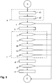
- Fig. 3 shows a third embodiment of a method according to the invention for determining the internal resistance of an electrical energy storage device.
- the exemplary embodiment is based on the method Fig. 2 a further, optional method step g.
- This method step g is carried out between the method step d and before the method step e.
- method step g it is checked whether the calculated zero-phase resistance R zp lies between a theoretical minimum limit value R i, min and a theoretical maximum limit value R i, max . If this is not the case, the procedure is again terminated prematurely.
- lead acid batteries are the minimum limit R i, min at about 2m ⁇ and the maximum limit R i, max at about 50m ⁇ .
- the method is identical to one of the in the FIGS. 1 . 2 or 3 pointed embodiments. Only in method step d, this alternative embodiment differs.
- the zero-phase resistance R zp is calculated in method step d by dividing the quadratic mean of the voltage peak values U p by the quadratic mean of the current peak values I p .
- Fig. 4 shows a fourth embodiment of a method according to the invention for determining the internal resistance of an electrical energy storage device.
- the method is based on the method according to Fig. 3 a further, optional method step h.
- the method step h is carried out after the method step d, but before the method step e.
- the zero-phase resistance R zp was calculated in method step d by forming a quotient of the voltage peak value U p and the current peak value I p .
- the calculated zero-phase resistance R zp is low-pass filtered, this functioning, for example, by means of a PT1 element.
- the optional method steps f, g and h can also proceed independently of one another in one method. So it is possible, for example, that starting from the method Fig. 1 only method step g between method step d and method step e expires, but method steps f and h are not performed.
- the internal resistance R i is determined by calculating the zero-phase resistance R zp .
- further resistance definitions such as a differential resistance, a 1 kHz resistance or an ohmic resistance, can be approximated. This is because the deviations between all these resistance definitions are limited to a certain extent. Therefore, for example, from the calculated zero-phase resistance R zp and the differential resistance can be determined with a certain tolerance.
Landscapes
- Physics & Mathematics (AREA)
- General Physics & Mathematics (AREA)
- Measurement Of Resistance Or Impedance (AREA)
- Tests Of Electric Status Of Batteries (AREA)
- Charge And Discharge Circuits For Batteries Or The Like (AREA)
- Electric Propulsion And Braking For Vehicles (AREA)
- Secondary Cells (AREA)
Description
- Der Innenwiderstand eines Energiespeichers kann auf verschiedene Weisen bestimmt werden. Im Fahrzeugbereich werden üblicherweise der differentielle Widerstand, der Nullphasen-Widerstand oder der ohmsche Widerstand berechnet und hieraus der Innenwiderstand bestimmt. Eine Methode zur Bestimmung des Innenwiderstands mittels der Berechnung des differentiellen Widerstands ist in der Offenlegungsschrift
WO 2006037694 A1 offenbart. - Weiterer Stand der Technik findet sich in den Offenlegungsschriften
EP1522866 undUS2012303301 . - Die Erfindung betrifft ein Verfahren zur Bestimmung eines Innenwiderstands eines elektrischen Energiespeichers. Erfindungsgemäß wird der Innenwiderstand bestimmt, indem ein Nullphasen-Widerstand berechnet wird, welcher wiederum als zu bestimmender Innenwiderstand bereitgestellt wird. Hierbei laufen folgende Verfahrensschritte nacheinander ab:
- a. Analog/Digital-Wandeln eines analogen Spannungssignals und eines analogen Stromsignals des elektrischen Energiespeichers, um digitale Spannungswerte und digitale Stromwerte zu erhalten,
- b. Filtern der digitalen Spannungswerte und der digitalen Stromwerte mit einem Bandpassfilter um die Nullphasen-Frequenz herum, um gefilterte Spannungswerte und Stromwerte zu erhalten,
- c. Prüfen ob folgende Berechnungsvoraussetzungen erfüllt sind:
- I. Der Bandpassfilter ist initialisiert,
- II. ein Stromspitzenwert mit seinem zugehörigen Zeitpunkt wird aus den gefilterten Stromwerten ermittelt,
- III. der Betrag des Stromspitzenwertes ist größer als der Betrag eines Schwellenstromwerts, wobei der Betrag des Schwellenstromwert größer als der Betrag eines minimalen Schwellenstromwerts ist, mit welchem ein Nullphasen-Widerstand mit einer vorgegebenen maximalen Abweichung vom tatsächlichen Innendwiderstand berechnet werden kann,
- IV. der gefilterter Spannungswert zum zuvor ermittelten Zeitpunkt ist ein Spannungsspitzenwert,
- V. der Stromspitzenwert und der Spannungsspitzenwert haben das gleiche Vorzeichen,
- d. Berechnen des Nullphasen-Widerstands aus dem Spannungsspitzenwert und dem Stromspitzenwert, falls das Verfahren zuvor noch nicht beendet wurde,
- e. Bereitstellen des Nullphasenwiderstands als zu bestimmender Innenwiderstand des elektrischen Energiespeichers, falls das Verfahren zuvor noch nicht beendet wurde.
- Vorteilhaft ist hierbei, dass bereits kleine Strom- bzw. Spannungsschwankungen als Anregung für den elektrischen Energiespeicher zur Berechnung des Nullphasen-Widerstands und somit zur Bestimmung des Innenwiderstands des elektrischen Energiespeichers ausreichen, wie dies beispielsweise während der Fahrt oder bei ausgeschaltetem Motor der Fall ist. Eine starke Anregung des elektrischen Energiespeichers auf Grund eines Motorstarts ist daher keine Voraussetzung mehr, um den Innenwiderstand bestimmen zu können. Dies ist insbesondere bei Hybrid- und Elektrofahrzeugen von Vorteil, die keinen klassischen Motorstart aufweisen. Zudem benötigt das Verfahren nur einen geringen Berechnungsaufwand im Vergleich zu anderen Verfahren zur Innenwiderstandsbestimmung, beispielsweise einem Verfahren mittels Spektralmethode bei welchem der Innenwiderstand durch diskrete FourierTransformation bestimmt wird. Das Verfahren ist außerdem für die Benutzung in einem eingebetteten System optimiert, beispielsweise in einem elektrischen Batteriesensor, und kann sowohl für aktive als auch für passive Bestimmung des Innenwiderstands eingesetzt werden. Eine aktive Bestimmung bezeichnet hierbei die Anregung des elektrischen Energiespeichers mit einer kontrollierten Wechselspannung bei spezifischen Frequenzen. Der Hauptvorteil liegt darin, dass der Innenwiderstand durchgehend und unabhängig von der Netzspannung berechnet werden kann. Jedoch benötigt die aktive Bestimmung eine komplexe Hardware mit Leistungselektronik und belastet zudem die Batterie. Eine passive Bestimmung bezeichnet dagegen die Anregung des elektrischen Energiespeichers durch eine Netzspannung eines Drehstromgenerators oder durch einen Verbraucher. Die Hardware-Anforderungen sind hierdurch geringer, da nur eine Messung des Stroms und der Spannung des Energiespeichers nötig sind. Dies kann beispielsweise durch einen Shunt oder einen Hallsensor umgesetzt werden. Da bei dieser passiven Bestimmung jedoch die Anregung des Energiespeichers nicht direkt kontrolliert wird, wird der Innenwiderstand nicht aktualisiert, falls die Berechnungsvoraussetzungen nicht erfüllt werden. Des Weiteren kann durch das Verändern des Schwellenstromwerts, die Genauigkeit der Bestimmung des Innenwiderstands eingestellt werden.
- Eine vorteilhafte Ausgestaltung des erfindungsgemäßen Verfahrens sieht vor, dass zwischen dem Verfahrensschritt a und dem Verfahrensschritt e ein weiterer Verfahrensschritt f abläuft, in welchem die Gültigkeit der digitalen Spannungswerte und der digitalen Stromwerte überprüft wird. Hierbei gelten die digitalen Spannungswerte und digitalen Stromwerte als gültig, falls der Verfahrensschritt a erfolgreich durchgeführt wurde. Bei einem ungültigen digitalen Spannungswert oder digitalen Stromwert wird dagegen das Verfahren beendet. Vorteilhaft ist hierbei, dass das Verfahren nur mit gültigen, das bedeutet fehlerfreien, Messwerten weitergeführt wird. Hierdurch kann bei fehlerhaften Messwerten zum einen der Berechnungsaufwand reduziert werden und zum anderen kann vermieden werden, dass ein fehlerhafter Nullphasen-Widerstand als Innenwiderstand bereitgestellt wird.
- Eine weitere vorteilhafte Ausgestaltung des erfindungsgemäßen Verfahrens sieht vor, dass der Stromspitzenwert oder auch der Spannungsspitzenwert mittels eines, insbesondere drei-elementigen, First In - First Out-Prinzips (FIFO) ermittelt werden. Vorteilhaft ist hierbei, dass das FIFO-Prinzip ein einfaches Mittel darstellt, um einen Spitzenwert aus mehreren Werten zu ermitteln. Hierdurch wird die für diesen Verfahrensschritt benötigte Rechenleistung gering gehalten.
- In einer vorteilhaften Ausgestaltung des erfindungsgemäßen Verfahrens ist vorgesehen, dass zwischen dem Verfahrensschritt d und dem Verfahrensschritt e ein weiterer Verfahrensschritt g abläuft, in welchem die Plausibilität des Nullphasen-Widerstands geprüft wird. Hierbei gilt der Nullphasen-Widerstand als plausibel, falls er zwischen einem theoretischen Minimal-Grenzwert und einem theoretischen Maximal-Grenzwert des zu erwartenden Innenwiderstands liegt. Ist dies nicht der Fall, wird das Verfahren beendet. Vorteilhaft ist hierbei, dass der berechnete Nullphasen-Widerstand nur dann im Verfahrensschritt e als Innenwiderstand bereitgestellt wird, falls er als plausibel eingestuft ist. Hierdurch kann das Bereitstellen eines fehlerhaften Nullphasen-Widerstands als Innenwiderstand vermieden werden.
- In einer weiteren vorteilhaften Ausgestaltung des erfindungsgemäßen Verfahrens ist vorgesehen, dass das Berechnen des Nullphasen-Widerstands im Verfahrensschritt d durch Bildung eines Quotienten aus Spannungsspitzenwert und Stromspitzenwert erfolgt. Vorteilhaft ist hierbei, dass dies eine einfache Möglichkeit zur Berechnung des Nullphasen-Widerstands darstellt und somit nur eine geringe Rechenkapazität erfordert.
- Eine vorteilhafte Ausführungsform des erfindungsgemäßen Verfahrens sieht vor, dass zwischen dem Verfahrensschritt d und dem Verfahrensschritt e ein weiterer Verfahrensschritt h abläuft, in welchem der berechnete Nullphasen-Widerstand tiefpassgefiltert wird, insbesondere mittels eines PT1-Glieds. Vorteilhaft ist hierbei, dass durch die Filterung die Standardabweichung reduziert werden kann, welche beispielsweise auf Grund von Messrauschen auftritt.
- Eine weitere vorteilhafte Ausgestaltung des erfindungsgemäßen Verfahrens sieht vor, dass das Berechnen des Nullphasen-Widerstands im Verfahrensschritt d durch Bildung eines Quotienten des quadratischen Mittels der Spannungsspitzenwerte zum quadratischen Mittel der Stromspitzenwerte erfolgt. Vorteilhaft ist hierbei, dass die Genauigkeit bei der Berechnung des Nullphasen-Widerstands durch diese Berechnungsweise nochmals gesteigert wird.
-
-
Fig. 1 zeigt ein erstes Ausführungsbeispiel eines erfindungsgemäßen Verfahrens zur Bestimmung des Innenwiderstands eines elektrischen Energiespeichers. -
Fig. 2 zeigt ein zweites Ausführungsbeispiel eines erfindungsgemäßen Verfahrens zur Bestimmung des Innenwiderstands eines elektrischen Energiespeichers. -
Fig. 3 zeigt ein drittes Ausführungsbeispiel eines erfindungsgemäßen Verfahrens zur Bestimmung des Innenwiderstands eines elektrischen Energiespeichers. -
Fig. 4 zeigt ein viertes Ausführungsbeispiel eines erfindungsgemäßen Verfahrens zur Bestimmung des Innenwiderstands eines elektrischen Energiespeichers. -
Fig. 1 zeigt ein erstes Ausführungsbeispiel eines erfindungsgemäßen Verfahrens zur Bestimmung des Innenwiderstands eines elektrischen Energiespeichers. Das Verfahren beginnt im Start S. Zuerst werden in einem Verfahrensschritt a ein analoges Spannungssignal Uanalog und ein analoges Stromsignal Ianalog des elektrischen Energiespeichers in digitale Spannungswerte U und digitale Stromwerte I umgewandelt. Diese Analog/Digital-Wandlung geschieht im Verfahrensschritt a durch einen ersten Teilschritt a1 und einen zweiten Teilschritt a2. Im ersten Teilschritt a1 werden das analoge Spannungssignal Uanalog und das analoge Stromsignal Ianalog tiefpassgefiltert, wobei dies beispielsweise mittels einen analogen Tiefpassfilters geschieht. Daraufhin wird im zweiten Teilschritt a2 das tiefpassgefilterte analoge Spannungssignal Uanalog und das tiefpassgefilterte analoge Stromsignal Ianalog abgetastet, um digitale Spannungswerte U und digitale Stromwerte I zu erhalten. Hierbei erfolgt das Abtasten für das analoge Spannungssignal Uanalog und das analoge Stromsignal Ianalog synchron und unter der Voraussetzung, dass eine Abtastfrequenz fTast mindestens doppelt so groß wie eine maximale Nullphasenfrequenz fzp, max ist. Die Tiefpassfilterung dient dabei dazu, dass die Bandbreite des abzutastenden Signals der Abtastrate genügt. Des Weiteren wird durch die Voraussetzung für die Abtastfrequenz fTast das Nyquist-Shannon-Abtasttheorem eingehalten. Die digitalen Spannungswerte U und die digitalen Stromwerte I werden in einem anschließenden Verfahrensschritt b gefiltert. Die Filterung geschieht hierbei mittels eines Bandpassfilters, welcher um eine Nullphasen-Frequenz fzp herum filtert. Bei dieser Nullphasen-Frequenz fzp ist der Impedanzwinkel in etwa null. Die Nullphasen-Frequenz fzp ist beispielsweise abhängig von der Art des Energiespeichers, der Temperatur und des Ladungszustands. Bei Bleibatterien liegt die Nullphasen-Frequenz fzp typscherweise zwischen 300Hz und 1kHz. Durch die Bandpassfilterung erhält man gefilterte Spannungswerte Ufilt und gefilterte Stromwerte Ifilt. In einem weiteren Verfahrensschritt c werden anschließend mehrere Berechnungsvoraussetzungen nacheinander geprüft. Sobald auch nur eine dieser Berechnungsvoraussetzungen nicht erfüllt ist, wird das Verfahren vorzeitig beendet. Das Beenden ist hierbei als Ende E dargestellt. Das Verfahren beginnt typischerweise nach dem Beenden wieder im Start S. Anhand der Berechnungsvoraussetzung I wird geprüft, ob der Bandpassfilter initialisiert ist. So ist beispielsweise bei einem Bandpassfilter n-ter Ordnung der Bandpassfilter erst nach n abgetasteten Werten initialisiert, wobei n hier eine natürliche Zahl, größer Null, darstellt. Durch die Berechnungsvoraussetzung II wird geprüft, ob ein Stromspitzenwert Ip aus den gefilterten Stromwerten Ifilt ermittelt werden kann. Der Stromspitzenwert Ip wird beispielsweise mittels eines, insbesondere drei-elementigen, FIFO-Prinzips ermittelt. Hierbei werden die zuletzt abgetasteten und anschließend gefilterten Stromwerte Ifilt miteinander verglichen. Kann hierbei einer der gefilterten Stromwerte Ifilt als Stromspitzenwert Ip ausgemacht werden, wird das zeitliche Auftreten des Stromspitzenwerts Ip als Zeitpunkt tp definiert. Wird dagegen kein Stromspitzenwert Ip ermittelt, wird beim nächsten Verfahrensdurchlauf wenigstens ein ältester, gefilterte Stromwert Ifilt durch wenigstens einen neuen, gefilterten Stromwert Ifilt ersetzt und versucht, aus den vorhandenen und neuen Werten ein Stromspitzenwert Ip zu ermitteln. Als dritte Berechnungsvoraussetzung III wird geprüft, ob der Betrag des Stromspitzenwerts Ip größer als der Betrag eines Schwellenstromwerts Ith ist. Hierbei kann der Schwellenstromwert Ith von Verfahrensdurchlauf zu Verfahrensdurchlauf verändert werden, vorausgesetzt, dass dessen Betrag stets größer als der Betrag eines minimalen Schwellenstromwerts Ith, min ist, mit welchem ein Nullphasen-Widerstand Rzp noch mit einer vorgegebenen, maximalen Abweichung vom tatsächlichen Innenwiderstands Ri des elektrischen Energiespeichers berechnet werden kann. So sollte beispielsweise die maximale Abweichung zwischen dem mittels eines Batteriesensors bestimmten Innenwiderstand Ri und einem tatsächlichen Ist-Wert des Innendwiderstands Ri nicht größer als 10% sein. Durch die Veränderung des Schwellenstromwerts Ith kann die Genauigkeit der Berechnung Nullphasen-Widerstands Rzp auf Kosten der Häufigkeit von dessen Berechnung angepasst werden. Hierbei gilt, je höher der Schwellenstrom Ith, desto genauer der berechnete Nullphasen-Widerstands Rzp und somit auch der bereitgestellte Innenwiderstand Ri, jedoch desto seltener die Nullphasen-Widerstands-Berechnung an sich. Anschließend wird mittels der Berechnungsvoraussetzung IV geprüft, ob der gefilterte Spannungswert Ufilt zum Zeitpunkt tp ein Spannungsspitzenwert Up ist. Dies wird beispielsweise wiederum mittels eines FIFO-Prinzips umgesetzt. Abschließend wird dann mit der Berechnungsvoraussetzung V geprüft, ob der Stromspitzenwert Ip und der Spannungsspitzenwert Up das gleiche Vorzeichen haben. Durch die Berechnungsvoraussetzungen und die Bandpassfilterung wird erreicht, dass sowohl der Stromspitzenwert Ip als auch das Spannungsspitzenwert Up im Wesentlichen aus einem Realteil bestehen und somit keinen bzw. nur einen sehr geringen Imaginärteil aufweisen. Dies bedeutet, dass die Phasenwinkel des abgetasteten analogen Strom- und des Spannungssignals entweder etwa 0° oder etwa 180° betragen. Hierdurch kann in einem anschließenden Verfahrensschritt d ein Nullphasen-Widerstand Rzp als Maß für den Innenwiderstand Ri berechnet werden. Die Berechnung des Nullphasen-Widerstands Rzp erfolgt dabei, indem der Spannungsspitzenwert Up durch den Stromspitzenwert IP geteilt wird. Anschließend wird in einem Verfahrensschritt e der berechnete Nullphasen-Widerstands Rzp als zu bestimmender Innendwiderstand Ri bereitgestellt und abschließend das Verfahren beendet. Nach dem Ende E wird das Verfahren, wie bereits erwähnt, typischerweise wieder neugestartet. Dies geschieht so lange, bis der Innenwiderstand Ri nicht mehr bestimmt soll. Zudem laufen im Normalfall mehrere dieser Verfahren zeitversetzt ab. So wird beispielsweise das analoge Spannungssignal Uanalog und das analoge Stromsignal Ianalog über eine bestimmte Dauer hinweg abgetastet und daraus im weiteren Verlauf des Verfahrens versucht, den Innenwiderstand Ri des Energiespeichers zu bestimmen, indem die Werte wie aufgezeigt weiterverarbeitet werden. Während dieser Weiterverarbeitung wird das Verfahren jedoch bereits erneut gestartet um das analoge Spannungssignal Uanalog und das analoge Stromsignal Ianalog auch weiterhin abzutasten und daraus wiederum den Innenwiderstand Ri zu bestimmen. -
Fig. 2 zeigt ein zweites Ausführungsbeispiel eines erfindungsgemäßen Verfahrens zur Bestimmung des Innenwiderstands eines elektrischen Energiespeichers. Das Verfahren läuft dabei identisch zu dem Verfahren nachFig. 1 ab. Allerdings wird zwischen dem Verfahrensschritt a und dem Verfahrensschritt b ein optionaler Verfahrensschritt f durchgeführt, in welchem geprüft wird, ob die Analog/Digital-Wandlung im Verfahrensschritt a erfolgreich durchgeführt wurde. Ist dies nicht der Fall, gelten die digitalen Spannungswerte U bzw. digitalen Stromwerte I als ungültig und das Verfahren wird beendet. Mögliche Gründe für eine fehlerhafte A/D-Wandlung sind beispielsweise auftretende Störsignale oder eine Neukonfiguration des A/D-Wandlers. Umgesetzt kann die Plausibilitätsprüfung beispielsweise, indem die digitalen Spannungswerte U und die digitalen Stromwerte I bei der A/D-Wandlung einen zusätzlichen, binären Status-Flag erhalten, welcher aussagt, ob die A/D-Wandlung erfolgreich war. Daraufhin muss im Verfahrensschritt f nur noch geprüft werden, ob der Status-Flag des jeweiligen Wertes gesetzt ist oder nicht. - In einem alternativen, bildlich nicht dargestellten Ausführungsbeispiel wird der Verfahrensschritt f nach dem Verfahrensschritt b, aber zumindest vor dem Verfahrensschritt e durchgeführt. In einem weiteren, nicht bildlich dargestellten Ausführungsbeispiel wird bei Beenden des Verfahrens auf Grund eines ungültigen, digitalen Stromwerts I oder auch eines ungültigen, digitalen Spannungswerts U der A/D-Wandler und der Tiefpassfilter reinitialisiert, bevor das Verfahren das nächste Mal gestartet wird.
-
Fig. 3 zeigt ein drittes Ausführungsbeispiel eines erfindungsgemäßen Verfahrens zur Bestimmung des Innenwiderstands eines elektrischen Energiespeichers. Das Ausführungsbeispiel weist ausgehend von dem Verfahren nachFig. 2 einen weiteren, optionalen Verfahrensschritt g auf. Dieser Verfahrensschritt g wird zwischen dem Verfahrensschritt d und vor dem Verfahrensschritt e durchgeführt. Im Verfahrensschritt g wird dabei geprüft, ob der berechnete Nullphasen-Widerstands Rzp zwischen einem theoretischen Minimal-Grenzwert Ri, min und einem theoretischen Maximal-Grenzwert Ri, max liegt. Ist dies nicht der Fall, wird das Verfahren wiederum vorzeitig beendet. Für Bleibatterien beispielsweise liegen der Minimal-Grenzwert Ri, min bei etwa 2mΩ und der Maximal-Grenzwert Ri, max bei etwa 50mΩ. - In einem nicht dargestellten, alternativen Ausführungsbeispiel verläuft das Verfahren identisch zu einem der in den
Figuren 1 ,2 oder3 aufgezeigten Ausführungsbeispiele. Lediglich im Verfahrensschritt d unterscheidet sich dieses alternative Ausführungsbeispiel. So wird hierbei der Nullphasen-Widerstands Rzp im Verfahrensschritt d berechnet, indem das quadratische Mittel der Spannungsspitzenwerte Up durch das quadratische Mittel der Stromspitzenwerte Ip geteilt wird. -
Fig. 4 zeigt ein viertes Ausführungsbeispiel eines erfindungsgemäßen Verfahrens zur Bestimmung des Innenwiderstands eines elektrischen Energiespeichers. Das Verfahren weist ausgehend von dem Verfahren nachFig. 3 einen weiteren, optionalen Verfahrensschritt h auf. Der Verfahrensschritt h wird nach dem Verfahrensschritt d, aber vor dem Verfahrensschritt e durchgeführt. Allerdings nur für den Fall, dass der Nullphasen-Widerstands Rzp im Verfahrensschritt d durch die Bildung eines Quotienten aus dem Spannungsspitzenwert Up und dem Stromspitzenwert Ip berechnet wurde. Im Verfahrensschritt h wird der berechnete Nullphasen-Widerstands Rzp tiefpassgefiltert, wobei dies beispielsweise mittels eines PT1-Glieds funktioniert. - In weiteren, alternativen, nicht bildlich dargestellten Ausführungsbeispielen können die optionalen Verfahrensschritte f, g und h auch unabhängig voneinander in einem Verfahren ablaufen. So ist es beispielsweise möglich, dass ausgehend vom Verfahren nach
Fig. 1 nur der Verfahrensschritt g zwischen dem Verfahrensschritt d und dem Verfahrensschritt e abläuft, die Verfahrensschritte f und h jedoch nicht durchgeführt werden. - In den zuvor genannten Ausführungsbeispielen wird der Innenwiderstand Ri bestimmt, indem der Nullphasen-Widerstands Rzp berechnet wird. Anhand des berechneten Nullphasen-Widerstands Rzp lassen sich allerdings auch weitere Widerstands-Definitionen, wie beispielsweise ein differentieller Widerstand, ein 1-kHz-Widerstand oder ein ohmscher Widerstand, näherungsweise bestimmen. Dies liegt darin begründet, dass die Abweichungen zwischen all diesen Widerstands-Definitionen in einem gewissen Maße begrenzt sind. Daher kann beispielsweise aus dem berechneten Nullphasen-Widerstand Rzp auch der differentielle Widerstand mit einer gewissen Toleranz bestimmt werden.
Claims (7)
- Verfahren zur Bestimmung eines Innenwiderstands (Ri) eines elektrischen Energiespeichers mit folgenden, nacheinander ablaufenden Verfahrensschritten:a. Analog-Digital-Wandeln eines analogen Spannungssignals (Uanalog) und eines analogen Stromsignals (Ianalog) des elektrischen Energiespeichers, um digitale Spannungswerte (U) und digitale Stromwerte (I) zu erhalten,b. Filtern der digitalen Spannungswerte (U) und der digitalen Stromwerte (I) mit einem Bandpassfilter um die Nullphasen-Frequenz (fzp) herum, um gefilterte Spannungswerte (Ufilt) und Stromwerte (Ifilt) zu erhalten,c. Prüfen ob folgende Berechnungsvoraussetzungen erfüllt sind:I. Der Bandpassfilter ist initialisiert,II. ein Stromspitzenwert (Ip) mit seinem zugehörigen Zeitpunkt (tp) wird aus den gefilterten Stromwerten (Ifilt) ermittelt,III. der Betrag des Stromspitzenwerts (Ip) ist größer als der Betrag eines Schwellenstromwerts (Ith), wobei der Betrag des Schwellenstromwerts (Ith) größer als der Betrag eines minimalen Schwellenstromwerts (Ith, min) ist, mit welchem ein Nullphasen-Widerstand (Rzp) mit einer vorgegebenen maximalen Abweichung vom tatsächlichen Innenwiderstand (Ri) berechnet werden kann,IV. der gefilterter Spannungswert (Ufilt) zum zuvor ermittelten Zeitpunkt (tp) ist ein Spannungsspitzenwert (Up),V. der Stromspitzenwert (Ip) und der Spannungsspitzenwert (Up) haben das gleiche Vorzeichen,wobei diese Berechnungsvoraussetzungen nacheinander geprüft werden, jedoch die Berechnungsvoraussetzung I auch an einer beliebigen anderen Stelle im Verfahrensschritt c geprüft werden kann und wobei das Verfahren beendet wird, falls eine der Berechnungsvoraussetzungen nicht erfüllt ist,d. Berechnen des Nullphasen-Widerstand (Rzp) aus dem Spannungsspitzenwert (Up) und dem Stromspitzenwert (Ip), falls das Verfahren zuvor noch nicht beendet wurde,e. Bereitstellen des Nullphasenwiderstands (Rzp) als zu bestimmender Innenwiderstand (Ri) des elektrischen Energiespeichers, falls das Verfahren zuvor noch nicht beendet wurde.
- Verfahren nach Anspruch 1, gekennzeichnet durch einen weiteren Verfahrensschritt:f. Überprüfen der Gültigkeit der digitalen Spannungswerte (U) und der digitalen Stromwerte (I), wobei die digitalen Spannungswert (U) und die digitalen Stromwerte (I) als gültig gelten, falls der Verfahrensschritt a erfolgreich durchgeführt wurde, und Beenden des Verfahrens bei einem ungültigen digitalen Spannungswert (U) oder einem ungültigen digitalen Stromwert (I),wobei der Verfahrensschritt f nach dem Verfahrensschritt a und vor dem Verfahrensschritt e abläuft.
- Verfahren nach einem der Ansprüche 1 oder 2, dadurch gekennzeichnet, dass der Stromspitzenwert (Ip) und/oder der Spannungsspitzenwert (Up) mittels eines, insbesondere drei-elementigen, FIFO-Prinzips ermittelt werden.
- Verfahren nach einem der vorherigen Ansprüche, gekennzeichnet durch einen weiteren Verfahrensschritt:g. Prüfen der Plausibilität des berechneten Nullphasen-Widerstands (Rzp), wobei dieser als plausibel gilt, falls er zwischen einem theoretischen Minimal-Grenzwert (Ri,min) und einem theoretischen Maximal-Grenzwert (Ri,max) liegt und Beenden des Verfahrens bei einem unplausiblen Nullphasen-Widerstand (Rzp),wobei der Verfahrensschritt g zwischen dem Verfahrensschritt d und dem Verfahrensschritt e abläuft.
- Verfahren nach einem der Ansprüche 1 bis 4, dadurch gekennzeichnet, dass das Berechnen des Nullphasenwiderstands (Rzp) im Verfahrensschritt d durch Bildung eines Quotienten aus Spannungsspitzenwert (Up) und Stromspitzenwert (Ip) erfolgt.
- Verfahren nach Anspruch 5, gekennzeichnet durch einen weiteren Verfahrensschritt:h. Tiefpassfiltern des berechneten Nullphasen-Widerstands (Rzp), insbesondere mittels eines PT1-Glieds,wobei der Verfahrensschritt h zwischen dem Verfahrensschritt d und dem Verfahrensschritt e abläuft.
- Verfahren nach einem der Ansprüche 1 bis 4, dadurch gekennzeichnet, dass das Berechnen des Nullphasenwiderstands (Rzp) im Verfahrensschritt d durch Bildung eines Quotienten aus einem quadratischen Mittel der Spannungsspitzenwerte (Up) und einem quadratischen Mittel der Stromspitzenwerte (Ip) erfolgt.
Applications Claiming Priority (2)
| Application Number | Priority Date | Filing Date | Title |
|---|---|---|---|
| DE102014217087.7A DE102014217087A1 (de) | 2014-08-27 | 2014-08-27 | Verfahren zur Bestimmung eines Innenwiderstands eines elektrischen Energiespeichers |
| PCT/EP2015/065336 WO2016030065A1 (de) | 2014-08-27 | 2015-07-06 | Verfahren zur bestimmung eines innenwiderstands eines elektrischen energiespeichers |
Publications (2)
| Publication Number | Publication Date |
|---|---|
| EP3186650A1 EP3186650A1 (de) | 2017-07-05 |
| EP3186650B1 true EP3186650B1 (de) | 2018-09-26 |
Family
ID=53510887
Family Applications (1)
| Application Number | Title | Priority Date | Filing Date |
|---|---|---|---|
| EP15734174.4A Active EP3186650B1 (de) | 2014-08-27 | 2015-07-06 | Verfahren zur bestimmung eines innenwiderstands eines elektrischen energiespeichers |
Country Status (7)
| Country | Link |
|---|---|
| US (1) | US10288695B2 (de) |
| EP (1) | EP3186650B1 (de) |
| JP (1) | JP6456482B2 (de) |
| CN (1) | CN106796268B (de) |
| DE (1) | DE102014217087A1 (de) |
| ES (1) | ES2703578T3 (de) |
| WO (1) | WO2016030065A1 (de) |
Families Citing this family (3)
| Publication number | Priority date | Publication date | Assignee | Title |
|---|---|---|---|---|
| CN107329091B (zh) * | 2017-07-13 | 2020-07-03 | 大唐恩智浦半导体有限公司 | 一种电池内部温度测量方法、装置和系统 |
| JP7262501B2 (ja) * | 2021-03-18 | 2023-04-21 | プライムプラネットエナジー&ソリューションズ株式会社 | 電池の状態算出装置および状態算出方法 |
| DE102021131645B4 (de) | 2021-12-01 | 2026-05-07 | Audi Aktiengesellschaft | Verfahren zur Beurteilung einer elektrischen Verbindung eines elektrischen Energiespeichers mit einem Bordnetz, sowie elektronisches Batteriebeurteilungssystem und Fahrzeug |
Family Cites Families (29)
| Publication number | Priority date | Publication date | Assignee | Title |
|---|---|---|---|---|
| GB2114758B (en) * | 1982-02-05 | 1985-07-31 | Rolls Royce | Ultrasonic flaw detector signal analyser |
| JPS63108284A (ja) * | 1986-10-24 | 1988-05-13 | Nissan Motor Co Ltd | 自動車用バツテリの診断装置 |
| JP3586285B2 (ja) * | 1992-05-13 | 2004-11-10 | ソニー株式会社 | 電池充放電装置 |
| JP3330704B2 (ja) * | 1993-11-05 | 2002-09-30 | 新電元工業株式会社 | バッテリの交流定電流充放電回路及びこれを用いたバッテリ試験装置 |
| JPH07322469A (ja) * | 1994-05-18 | 1995-12-08 | Mitsubishi Electric Corp | 地絡保護継電器 |
| US6002238A (en) * | 1998-09-11 | 1999-12-14 | Champlin; Keith S. | Method and apparatus for measuring complex impedance of cells and batteries |
| DE19853897A1 (de) * | 1998-11-23 | 2000-05-25 | Bosch Gmbh Robert | Verfahren und Anordnung zur Kompensation von Phasenverzögerungen |
| US6252406B1 (en) * | 2000-01-12 | 2001-06-26 | Honeywell International Inc. | Programmable event limit detector for computer system power control |
| DE10205120B4 (de) * | 2001-02-13 | 2004-12-16 | Akkumulatorenfabrik Moll Gmbh & Co. Kg | Verfahren und Vorrichtung zur Ermittlung des Innenwiderstandes einer Batterie, insbesondere einer Starterbatterie für ein Kraftfahrzeug |
| JP4032934B2 (ja) * | 2002-11-15 | 2008-01-16 | ソニー株式会社 | 電池容量算出方法、電池容量算出装置、及び電池容量算出プログラム |
| US7518339B2 (en) * | 2003-01-30 | 2009-04-14 | Robert Bosch Gmbh | State variable and parameter estimator comprising several partial models for an electrical energy storage device |
| DE10345057B4 (de) * | 2003-09-26 | 2005-09-15 | Rheinisch-Westfälisch-Technische Hochschule Aachen | Verfahren und Vorrichtung zur Bestimmung des Ladezustandes einer Batterie |
| DE10347317A1 (de) * | 2003-10-08 | 2005-05-12 | Tech Gmbh D | Einrichtung und Verfahren zur Bestimmung des Innenwiderstandes einer Batterie |
| DE102005035416A1 (de) * | 2004-10-05 | 2006-04-06 | Robert Bosch Gmbh | Verfahren zur Rekonstruktion eines elektrischen Signals |
| JP2007024740A (ja) * | 2005-07-20 | 2007-02-01 | Nissan Motor Co Ltd | 二次電池の充電率推定装置 |
| JP4387391B2 (ja) * | 2006-09-08 | 2009-12-16 | パナソニック株式会社 | 蓄電装置 |
| US8159228B2 (en) * | 2008-12-18 | 2012-04-17 | Lear Corporation | Method for determining battery internal resistance |
| JP5381664B2 (ja) * | 2009-12-02 | 2014-01-08 | トヨタ自動車株式会社 | 組電池の異常検出装置 |
| JP2011137681A (ja) | 2009-12-28 | 2011-07-14 | Panasonic Corp | インピーダンス検出回路、電池電源装置、及び電池利用システム |
| KR20110134019A (ko) * | 2010-06-08 | 2011-12-14 | 현대자동차주식회사 | 차량용 배터리의 셀 열화 진단 방법 |
| JP5558941B2 (ja) * | 2010-06-30 | 2014-07-23 | 三洋電機株式会社 | 電池の内部抵抗の検出方法 |
| JP2012042429A (ja) * | 2010-08-23 | 2012-03-01 | Honda Motor Co Ltd | 蓄電装置の開路電圧検出装置および残容量検出装置 |
| DE102010062116A1 (de) * | 2010-11-29 | 2012-05-31 | Bayerische Motoren Werke Aktiengesellschaft | Energiespeichervorrichtung für ein Kraftfahrzeug |
| DE102011003690A1 (de) * | 2011-02-07 | 2012-08-09 | Robert Bosch Gmbh | Verfahren zur Bestimmung eines Batterie-Innenwiderstands |
| WO2012118005A1 (ja) * | 2011-02-28 | 2012-09-07 | 三洋電機株式会社 | 電池の状態検出装置、電源装置、移動体、充電装置、蓄電パック、及び検出装置 |
| KR101222207B1 (ko) | 2011-05-25 | 2013-01-15 | 삼성에스디아이 주식회사 | 배터리 내부 저항 추정 장치 및 그를 포함하는 배터리 팩 |
| US10109999B2 (en) * | 2012-11-02 | 2018-10-23 | Raytheon Company | Technology for extending a radio frequency (RF) bandwidth of an envelope tracking (ET) power amplifier (PA) |
| KR101438958B1 (ko) * | 2012-12-20 | 2014-09-15 | 현대오트론 주식회사 | 연료전지 스택의 주입 전류 생성 방법 |
| JP5631444B1 (ja) * | 2013-05-27 | 2014-11-26 | タナシン電機株式会社 | 漏洩電流算出装置及び漏洩電流算出方法 |
-
2014
- 2014-08-27 DE DE102014217087.7A patent/DE102014217087A1/de not_active Ceased
-
2015
- 2015-07-06 EP EP15734174.4A patent/EP3186650B1/de active Active
- 2015-07-06 CN CN201580046274.7A patent/CN106796268B/zh active Active
- 2015-07-06 ES ES15734174T patent/ES2703578T3/es active Active
- 2015-07-06 JP JP2017511733A patent/JP6456482B2/ja active Active
- 2015-07-06 WO PCT/EP2015/065336 patent/WO2016030065A1/de not_active Ceased
- 2015-07-06 US US15/506,541 patent/US10288695B2/en active Active
Non-Patent Citations (1)
| Title |
|---|
| None * |
Also Published As
| Publication number | Publication date |
|---|---|
| CN106796268A (zh) | 2017-05-31 |
| ES2703578T3 (es) | 2019-03-11 |
| DE102014217087A1 (de) | 2016-03-03 |
| CN106796268B (zh) | 2019-07-16 |
| US20170254860A1 (en) | 2017-09-07 |
| JP6456482B2 (ja) | 2019-01-23 |
| WO2016030065A1 (de) | 2016-03-03 |
| US10288695B2 (en) | 2019-05-14 |
| JP2017528710A (ja) | 2017-09-28 |
| EP3186650A1 (de) | 2017-07-05 |
Similar Documents
| Publication | Publication Date | Title |
|---|---|---|
| EP1266237B1 (de) | Verfahren und anordnung zur bestimmung des ladezustandes einer batterie | |
| EP1590679B1 (de) | Zustandsgrössen- und parameterschätzer mit mehreren teilmodellen für einen elektrischen energiespeicher | |
| EP3275040B1 (de) | Verfahren und vorrichtung zum formieren einer batterie | |
| DE102016122115B3 (de) | Schaltzustand eines mechanischen schalters | |
| DE102009046500B4 (de) | Verfahren zum Bestimmen des Innenwiderstands einer Batterie | |
| DE102018221621A1 (de) | Masseschluss-Erfassungsvorrichtung | |
| EP2487499A1 (de) | Echtzeitfähige Batteriezellensimulation | |
| DE102015101074B4 (de) | Verfahren und Vorrichtung zur Bestimmung einer Isolationsgröße sowie Kraftfahrzeug mit dieser Vorrichtung | |
| DE112011104614T5 (de) | Hybridelektrofahrzeugsystem und Verfahren zu seiner Steuerung | |
| DE102018217003A1 (de) | Vorrichtung zur Erfassung eines Erdungsfehlers | |
| DE102009003345A1 (de) | System und Verfahren zum Abschätzen des Ladezustands eines elektrochemischen Energiespeichers | |
| EP2721703B1 (de) | Verfahren und vorrichtung zur sicheren überwachung eines drehstrommotors | |
| DE102009001300A1 (de) | Verfahren und Vorrichtung zur Ermittlung einer charakteristischen Größe zur Erkennung der Bordnetzstabilität | |
| WO2013029774A2 (de) | Verfahren und vorrichtung zum laden eines energiespeichers eines fahrzeugs | |
| EP2318853B1 (de) | Verfahren zur berechnung des ladezustandes einer batterie | |
| EP3475713B1 (de) | Verfahren zur bestimmung des alters eines elektrochemischen energiespeichers | |
| EP3186650A1 (de) | Verfahren zur bestimmung eines innenwiderstands eines elektrischen energiespeichers | |
| WO2019072488A1 (de) | Energiespeichereinrichtung sowie vorrichtung und verfahren zur bestimmung einer kapazität einer energiespeichereinrichtung | |
| DE102021101693B3 (de) | Verfahren zur Messimpuls-Fehlererkennung und Verfahren zur Bestimmung einer Netzableitkapazität für die Anwendung in einem Verfahren zur Isolationsüberwachung in einem ungeerdeten Stromversorgungssystem | |
| DE102013209389A1 (de) | Verfahren zur Überwachung eines Zustands eines Akkumulators auf Basis eines den jeweiligen Zustand des Akkumulator kennzeichnenden Zustandswertes | |
| DE102010031050A1 (de) | Verfahren und Vorrichtung zum Betreiben eines Energiespeichers | |
| DE102018114960A1 (de) | Verfahren zum Ermitteln eines Offsets eines Rotorlagegebers, Steuerungseinrichtung für einen Stromrichter und elektrische Maschine für ein Fahrzeug | |
| EP3123185B1 (de) | Elektronischer batteriesensor und verfahren zur bestimmung eines innenwiderstandes einer batterie | |
| WO2017162384A1 (de) | Verfahren zum bestimmen eines fehlerzustands, batteriesensor und fahrzeugbordnetz | |
| WO2020207619A1 (de) | Verfahren zur ermittlung von kapazitäten von ableitkondensatoren in einem ladekabel |
Legal Events
| Date | Code | Title | Description |
|---|---|---|---|
| STAA | Information on the status of an ep patent application or granted ep patent |
Free format text: STATUS: THE INTERNATIONAL PUBLICATION HAS BEEN MADE |
|
| PUAI | Public reference made under article 153(3) epc to a published international application that has entered the european phase |
Free format text: ORIGINAL CODE: 0009012 |
|
| STAA | Information on the status of an ep patent application or granted ep patent |
Free format text: STATUS: REQUEST FOR EXAMINATION WAS MADE |
|
| 17P | Request for examination filed |
Effective date: 20170327 |
|
| AK | Designated contracting states |
Kind code of ref document: A1 Designated state(s): AL AT BE BG CH CY CZ DE DK EE ES FI FR GB GR HR HU IE IS IT LI LT LU LV MC MK MT NL NO PL PT RO RS SE SI SK SM TR |
|
| AX | Request for extension of the european patent |
Extension state: BA ME |
|
| DAV | Request for validation of the european patent (deleted) | ||
| DAX | Request for extension of the european patent (deleted) | ||
| GRAP | Despatch of communication of intention to grant a patent |
Free format text: ORIGINAL CODE: EPIDOSNIGR1 |
|
| STAA | Information on the status of an ep patent application or granted ep patent |
Free format text: STATUS: GRANT OF PATENT IS INTENDED |
|
| INTG | Intention to grant announced |
Effective date: 20180509 |
|
| GRAS | Grant fee paid |
Free format text: ORIGINAL CODE: EPIDOSNIGR3 |
|
| GRAA | (expected) grant |
Free format text: ORIGINAL CODE: 0009210 |
|
| STAA | Information on the status of an ep patent application or granted ep patent |
Free format text: STATUS: THE PATENT HAS BEEN GRANTED |
|
| AK | Designated contracting states |
Kind code of ref document: B1 Designated state(s): AL AT BE BG CH CY CZ DE DK EE ES FI FR GB GR HR HU IE IS IT LI LT LU LV MC MK MT NL NO PL PT RO RS SE SI SK SM TR |
|
| REG | Reference to a national code |
Ref country code: GB Ref legal event code: FG4D Free format text: NOT ENGLISH |
|
| REG | Reference to a national code |
Ref country code: CH Ref legal event code: EP |
|
| REG | Reference to a national code |
Ref country code: AT Ref legal event code: REF Ref document number: 1046659 Country of ref document: AT Kind code of ref document: T Effective date: 20181015 |
|
| REG | Reference to a national code |
Ref country code: IE Ref legal event code: FG4D Free format text: LANGUAGE OF EP DOCUMENT: GERMAN |
|
| REG | Reference to a national code |
Ref country code: DE Ref legal event code: R096 Ref document number: 502015006106 Country of ref document: DE |
|
| REG | Reference to a national code |
Ref country code: NL Ref legal event code: MP Effective date: 20180926 |
|
| PG25 | Lapsed in a contracting state [announced via postgrant information from national office to epo] |
Ref country code: FI Free format text: LAPSE BECAUSE OF FAILURE TO SUBMIT A TRANSLATION OF THE DESCRIPTION OR TO PAY THE FEE WITHIN THE PRESCRIBED TIME-LIMIT Effective date: 20180926 Ref country code: LT Free format text: LAPSE BECAUSE OF FAILURE TO SUBMIT A TRANSLATION OF THE DESCRIPTION OR TO PAY THE FEE WITHIN THE PRESCRIBED TIME-LIMIT Effective date: 20180926 Ref country code: BG Free format text: LAPSE BECAUSE OF FAILURE TO SUBMIT A TRANSLATION OF THE DESCRIPTION OR TO PAY THE FEE WITHIN THE PRESCRIBED TIME-LIMIT Effective date: 20181226 Ref country code: NO Free format text: LAPSE BECAUSE OF FAILURE TO SUBMIT A TRANSLATION OF THE DESCRIPTION OR TO PAY THE FEE WITHIN THE PRESCRIBED TIME-LIMIT Effective date: 20181226 Ref country code: GR Free format text: LAPSE BECAUSE OF FAILURE TO SUBMIT A TRANSLATION OF THE DESCRIPTION OR TO PAY THE FEE WITHIN THE PRESCRIBED TIME-LIMIT Effective date: 20181227 Ref country code: RS Free format text: LAPSE BECAUSE OF FAILURE TO SUBMIT A TRANSLATION OF THE DESCRIPTION OR TO PAY THE FEE WITHIN THE PRESCRIBED TIME-LIMIT Effective date: 20180926 Ref country code: SE Free format text: LAPSE BECAUSE OF FAILURE TO SUBMIT A TRANSLATION OF THE DESCRIPTION OR TO PAY THE FEE WITHIN THE PRESCRIBED TIME-LIMIT Effective date: 20180926 |
|
| REG | Reference to a national code |
Ref country code: LT Ref legal event code: MG4D |
|
| PG25 | Lapsed in a contracting state [announced via postgrant information from national office to epo] |
Ref country code: AL Free format text: LAPSE BECAUSE OF FAILURE TO SUBMIT A TRANSLATION OF THE DESCRIPTION OR TO PAY THE FEE WITHIN THE PRESCRIBED TIME-LIMIT Effective date: 20180926 Ref country code: LV Free format text: LAPSE BECAUSE OF FAILURE TO SUBMIT A TRANSLATION OF THE DESCRIPTION OR TO PAY THE FEE WITHIN THE PRESCRIBED TIME-LIMIT Effective date: 20180926 Ref country code: HR Free format text: LAPSE BECAUSE OF FAILURE TO SUBMIT A TRANSLATION OF THE DESCRIPTION OR TO PAY THE FEE WITHIN THE PRESCRIBED TIME-LIMIT Effective date: 20180926 |
|
| REG | Reference to a national code |
Ref country code: ES Ref legal event code: FG2A Ref document number: 2703578 Country of ref document: ES Kind code of ref document: T3 Effective date: 20190311 |
|
| PG25 | Lapsed in a contracting state [announced via postgrant information from national office to epo] |
Ref country code: IS Free format text: LAPSE BECAUSE OF FAILURE TO SUBMIT A TRANSLATION OF THE DESCRIPTION OR TO PAY THE FEE WITHIN THE PRESCRIBED TIME-LIMIT Effective date: 20190126 Ref country code: EE Free format text: LAPSE BECAUSE OF FAILURE TO SUBMIT A TRANSLATION OF THE DESCRIPTION OR TO PAY THE FEE WITHIN THE PRESCRIBED TIME-LIMIT Effective date: 20180926 Ref country code: PL Free format text: LAPSE BECAUSE OF FAILURE TO SUBMIT A TRANSLATION OF THE DESCRIPTION OR TO PAY THE FEE WITHIN THE PRESCRIBED TIME-LIMIT Effective date: 20180926 Ref country code: CZ Free format text: LAPSE BECAUSE OF FAILURE TO SUBMIT A TRANSLATION OF THE DESCRIPTION OR TO PAY THE FEE WITHIN THE PRESCRIBED TIME-LIMIT Effective date: 20180926 Ref country code: RO Free format text: LAPSE BECAUSE OF FAILURE TO SUBMIT A TRANSLATION OF THE DESCRIPTION OR TO PAY THE FEE WITHIN THE PRESCRIBED TIME-LIMIT Effective date: 20180926 Ref country code: NL Free format text: LAPSE BECAUSE OF FAILURE TO SUBMIT A TRANSLATION OF THE DESCRIPTION OR TO PAY THE FEE WITHIN THE PRESCRIBED TIME-LIMIT Effective date: 20180926 |
|
| PG25 | Lapsed in a contracting state [announced via postgrant information from national office to epo] |
Ref country code: SK Free format text: LAPSE BECAUSE OF FAILURE TO SUBMIT A TRANSLATION OF THE DESCRIPTION OR TO PAY THE FEE WITHIN THE PRESCRIBED TIME-LIMIT Effective date: 20180926 Ref country code: PT Free format text: LAPSE BECAUSE OF FAILURE TO SUBMIT A TRANSLATION OF THE DESCRIPTION OR TO PAY THE FEE WITHIN THE PRESCRIBED TIME-LIMIT Effective date: 20190126 Ref country code: SM Free format text: LAPSE BECAUSE OF FAILURE TO SUBMIT A TRANSLATION OF THE DESCRIPTION OR TO PAY THE FEE WITHIN THE PRESCRIBED TIME-LIMIT Effective date: 20180926 |
|
| REG | Reference to a national code |
Ref country code: DE Ref legal event code: R097 Ref document number: 502015006106 Country of ref document: DE |
|
| PG25 | Lapsed in a contracting state [announced via postgrant information from national office to epo] |
Ref country code: DK Free format text: LAPSE BECAUSE OF FAILURE TO SUBMIT A TRANSLATION OF THE DESCRIPTION OR TO PAY THE FEE WITHIN THE PRESCRIBED TIME-LIMIT Effective date: 20180926 |
|
| PLBE | No opposition filed within time limit |
Free format text: ORIGINAL CODE: 0009261 |
|
| STAA | Information on the status of an ep patent application or granted ep patent |
Free format text: STATUS: NO OPPOSITION FILED WITHIN TIME LIMIT |
|
| 26N | No opposition filed |
Effective date: 20190627 |
|
| PG25 | Lapsed in a contracting state [announced via postgrant information from national office to epo] |
Ref country code: SI Free format text: LAPSE BECAUSE OF FAILURE TO SUBMIT A TRANSLATION OF THE DESCRIPTION OR TO PAY THE FEE WITHIN THE PRESCRIBED TIME-LIMIT Effective date: 20180926 |
|
| PG25 | Lapsed in a contracting state [announced via postgrant information from national office to epo] |
Ref country code: MC Free format text: LAPSE BECAUSE OF FAILURE TO SUBMIT A TRANSLATION OF THE DESCRIPTION OR TO PAY THE FEE WITHIN THE PRESCRIBED TIME-LIMIT Effective date: 20180926 |
|
| REG | Reference to a national code |
Ref country code: CH Ref legal event code: PL |
|
| GBPC | Gb: european patent ceased through non-payment of renewal fee |
Effective date: 20190706 |
|
| PG25 | Lapsed in a contracting state [announced via postgrant information from national office to epo] |
Ref country code: TR Free format text: LAPSE BECAUSE OF FAILURE TO SUBMIT A TRANSLATION OF THE DESCRIPTION OR TO PAY THE FEE WITHIN THE PRESCRIBED TIME-LIMIT Effective date: 20180926 |
|
| REG | Reference to a national code |
Ref country code: BE Ref legal event code: MM Effective date: 20190731 |
|
| PG25 | Lapsed in a contracting state [announced via postgrant information from national office to epo] |
Ref country code: GB Free format text: LAPSE BECAUSE OF NON-PAYMENT OF DUE FEES Effective date: 20190706 |
|
| PG25 | Lapsed in a contracting state [announced via postgrant information from national office to epo] |
Ref country code: LI Free format text: LAPSE BECAUSE OF NON-PAYMENT OF DUE FEES Effective date: 20190731 Ref country code: LU Free format text: LAPSE BECAUSE OF NON-PAYMENT OF DUE FEES Effective date: 20190706 Ref country code: CH Free format text: LAPSE BECAUSE OF NON-PAYMENT OF DUE FEES Effective date: 20190731 Ref country code: BE Free format text: LAPSE BECAUSE OF NON-PAYMENT OF DUE FEES Effective date: 20190731 |
|
| PG25 | Lapsed in a contracting state [announced via postgrant information from national office to epo] |
Ref country code: IE Free format text: LAPSE BECAUSE OF NON-PAYMENT OF DUE FEES Effective date: 20190706 |
|
| PG25 | Lapsed in a contracting state [announced via postgrant information from national office to epo] |
Ref country code: CY Free format text: LAPSE BECAUSE OF FAILURE TO SUBMIT A TRANSLATION OF THE DESCRIPTION OR TO PAY THE FEE WITHIN THE PRESCRIBED TIME-LIMIT Effective date: 20180926 |
|
| PG25 | Lapsed in a contracting state [announced via postgrant information from national office to epo] |
Ref country code: MT Free format text: LAPSE BECAUSE OF FAILURE TO SUBMIT A TRANSLATION OF THE DESCRIPTION OR TO PAY THE FEE WITHIN THE PRESCRIBED TIME-LIMIT Effective date: 20180926 Ref country code: HU Free format text: LAPSE BECAUSE OF FAILURE TO SUBMIT A TRANSLATION OF THE DESCRIPTION OR TO PAY THE FEE WITHIN THE PRESCRIBED TIME-LIMIT; INVALID AB INITIO Effective date: 20150706 |
|
| REG | Reference to a national code |
Ref country code: AT Ref legal event code: MM01 Ref document number: 1046659 Country of ref document: AT Kind code of ref document: T Effective date: 20200706 |
|
| PG25 | Lapsed in a contracting state [announced via postgrant information from national office to epo] |
Ref country code: AT Free format text: LAPSE BECAUSE OF NON-PAYMENT OF DUE FEES Effective date: 20200706 |
|
| PG25 | Lapsed in a contracting state [announced via postgrant information from national office to epo] |
Ref country code: MK Free format text: LAPSE BECAUSE OF FAILURE TO SUBMIT A TRANSLATION OF THE DESCRIPTION OR TO PAY THE FEE WITHIN THE PRESCRIBED TIME-LIMIT Effective date: 20180926 |
|
| P01 | Opt-out of the competence of the unified patent court (upc) registered |
Effective date: 20230509 |
|
| PGFP | Annual fee paid to national office [announced via postgrant information from national office to epo] |
Ref country code: ES Payment date: 20250819 Year of fee payment: 11 |
|
| PGFP | Annual fee paid to national office [announced via postgrant information from national office to epo] |
Ref country code: DE Payment date: 20250924 Year of fee payment: 11 |
|
| PGFP | Annual fee paid to national office [announced via postgrant information from national office to epo] |
Ref country code: IT Payment date: 20250731 Year of fee payment: 11 |
|
| PGFP | Annual fee paid to national office [announced via postgrant information from national office to epo] |
Ref country code: FR Payment date: 20250723 Year of fee payment: 11 |