EP3185326A1 - Display panel with luminance efficiency improvement, display device, and method of fabricating the display panel - Google Patents
Display panel with luminance efficiency improvement, display device, and method of fabricating the display panel Download PDFInfo
- Publication number
- EP3185326A1 EP3185326A1 EP16184623.3A EP16184623A EP3185326A1 EP 3185326 A1 EP3185326 A1 EP 3185326A1 EP 16184623 A EP16184623 A EP 16184623A EP 3185326 A1 EP3185326 A1 EP 3185326A1
- Authority
- EP
- European Patent Office
- Prior art keywords
- substrate
- partitions
- display panel
- bank
- refractive index
- Prior art date
- Legal status (The legal status is an assumption and is not a legal conclusion. Google has not performed a legal analysis and makes no representation as to the accuracy of the status listed.)
- Granted
Links
Images







Classifications
-
- H—ELECTRICITY
- H10—SEMICONDUCTOR DEVICES; ELECTRIC SOLID-STATE DEVICES NOT OTHERWISE PROVIDED FOR
- H10K—ORGANIC ELECTRIC SOLID-STATE DEVICES
- H10K59/00—Integrated devices, or assemblies of multiple devices, comprising at least one organic light-emitting element covered by group H10K50/00
- H10K59/10—OLED displays
- H10K59/12—Active-matrix OLED [AMOLED] displays
- H10K59/122—Pixel-defining structures or layers, e.g. banks
-
- G—PHYSICS
- G09—EDUCATION; CRYPTOGRAPHY; DISPLAY; ADVERTISING; SEALS
- G09G—ARRANGEMENTS OR CIRCUITS FOR CONTROL OF INDICATING DEVICES USING STATIC MEANS TO PRESENT VARIABLE INFORMATION
- G09G3/00—Control arrangements or circuits, of interest only in connection with visual indicators other than cathode-ray tubes
- G09G3/20—Control arrangements or circuits, of interest only in connection with visual indicators other than cathode-ray tubes for presentation of an assembly of a number of characters, e.g. a page, by composing the assembly by combination of individual elements arranged in a matrix no fixed position being assigned to or needed to be assigned to the individual characters or partial characters
- G09G3/22—Control arrangements or circuits, of interest only in connection with visual indicators other than cathode-ray tubes for presentation of an assembly of a number of characters, e.g. a page, by composing the assembly by combination of individual elements arranged in a matrix no fixed position being assigned to or needed to be assigned to the individual characters or partial characters using controlled light sources
- G09G3/30—Control arrangements or circuits, of interest only in connection with visual indicators other than cathode-ray tubes for presentation of an assembly of a number of characters, e.g. a page, by composing the assembly by combination of individual elements arranged in a matrix no fixed position being assigned to or needed to be assigned to the individual characters or partial characters using controlled light sources using electroluminescent panels
- G09G3/32—Control arrangements or circuits, of interest only in connection with visual indicators other than cathode-ray tubes for presentation of an assembly of a number of characters, e.g. a page, by composing the assembly by combination of individual elements arranged in a matrix no fixed position being assigned to or needed to be assigned to the individual characters or partial characters using controlled light sources using electroluminescent panels semiconductive, e.g. using light-emitting diodes [LED]
- G09G3/3208—Control arrangements or circuits, of interest only in connection with visual indicators other than cathode-ray tubes for presentation of an assembly of a number of characters, e.g. a page, by composing the assembly by combination of individual elements arranged in a matrix no fixed position being assigned to or needed to be assigned to the individual characters or partial characters using controlled light sources using electroluminescent panels semiconductive, e.g. using light-emitting diodes [LED] organic, e.g. using organic light-emitting diodes [OLED]
-
- H—ELECTRICITY
- H10—SEMICONDUCTOR DEVICES; ELECTRIC SOLID-STATE DEVICES NOT OTHERWISE PROVIDED FOR
- H10K—ORGANIC ELECTRIC SOLID-STATE DEVICES
- H10K50/00—Organic light-emitting devices
- H10K50/80—Constructional details
- H10K50/85—Arrangements for extracting light from the devices
- H10K50/856—Arrangements for extracting light from the devices comprising reflective means
-
- H—ELECTRICITY
- H10—SEMICONDUCTOR DEVICES; ELECTRIC SOLID-STATE DEVICES NOT OTHERWISE PROVIDED FOR
- H10K—ORGANIC ELECTRIC SOLID-STATE DEVICES
- H10K50/00—Organic light-emitting devices
- H10K50/80—Constructional details
- H10K50/85—Arrangements for extracting light from the devices
- H10K50/858—Arrangements for extracting light from the devices comprising refractive means, e.g. lenses
-
- H—ELECTRICITY
- H10—SEMICONDUCTOR DEVICES; ELECTRIC SOLID-STATE DEVICES NOT OTHERWISE PROVIDED FOR
- H10K—ORGANIC ELECTRIC SOLID-STATE DEVICES
- H10K50/00—Organic light-emitting devices
- H10K50/80—Constructional details
- H10K50/86—Arrangements for improving contrast, e.g. preventing reflection of ambient light
- H10K50/865—Arrangements for improving contrast, e.g. preventing reflection of ambient light comprising light absorbing layers, e.g. light-blocking layers
-
- H—ELECTRICITY
- H10—SEMICONDUCTOR DEVICES; ELECTRIC SOLID-STATE DEVICES NOT OTHERWISE PROVIDED FOR
- H10K—ORGANIC ELECTRIC SOLID-STATE DEVICES
- H10K59/00—Integrated devices, or assemblies of multiple devices, comprising at least one organic light-emitting element covered by group H10K50/00
- H10K59/30—Devices specially adapted for multicolour light emission
- H10K59/38—Devices specially adapted for multicolour light emission comprising colour filters or colour changing media [CCM]
-
- H—ELECTRICITY
- H10—SEMICONDUCTOR DEVICES; ELECTRIC SOLID-STATE DEVICES NOT OTHERWISE PROVIDED FOR
- H10K—ORGANIC ELECTRIC SOLID-STATE DEVICES
- H10K59/00—Integrated devices, or assemblies of multiple devices, comprising at least one organic light-emitting element covered by group H10K50/00
- H10K59/80—Constructional details
- H10K59/875—Arrangements for extracting light from the devices
- H10K59/878—Arrangements for extracting light from the devices comprising reflective means
-
- H—ELECTRICITY
- H10—SEMICONDUCTOR DEVICES; ELECTRIC SOLID-STATE DEVICES NOT OTHERWISE PROVIDED FOR
- H10K—ORGANIC ELECTRIC SOLID-STATE DEVICES
- H10K59/00—Integrated devices, or assemblies of multiple devices, comprising at least one organic light-emitting element covered by group H10K50/00
- H10K59/80—Constructional details
- H10K59/875—Arrangements for extracting light from the devices
- H10K59/879—Arrangements for extracting light from the devices comprising refractive means, e.g. lenses
-
- G—PHYSICS
- G09—EDUCATION; CRYPTOGRAPHY; DISPLAY; ADVERTISING; SEALS
- G09G—ARRANGEMENTS OR CIRCUITS FOR CONTROL OF INDICATING DEVICES USING STATIC MEANS TO PRESENT VARIABLE INFORMATION
- G09G2300/00—Aspects of the constitution of display devices
- G09G2300/04—Structural and physical details of display devices
- G09G2300/0439—Pixel structures
- G09G2300/0452—Details of colour pixel setup, e.g. pixel composed of a red, a blue and two green components
-
- H—ELECTRICITY
- H10—SEMICONDUCTOR DEVICES; ELECTRIC SOLID-STATE DEVICES NOT OTHERWISE PROVIDED FOR
- H10K—ORGANIC ELECTRIC SOLID-STATE DEVICES
- H10K2102/00—Constructional details relating to the organic devices covered by this subclass
- H10K2102/301—Details of OLEDs
-
- H—ELECTRICITY
- H10—SEMICONDUCTOR DEVICES; ELECTRIC SOLID-STATE DEVICES NOT OTHERWISE PROVIDED FOR
- H10K—ORGANIC ELECTRIC SOLID-STATE DEVICES
- H10K59/00—Integrated devices, or assemblies of multiple devices, comprising at least one organic light-emitting element covered by group H10K50/00
- H10K59/10—OLED displays
- H10K59/12—Active-matrix OLED [AMOLED] displays
- H10K59/1201—Manufacture or treatment
Definitions
- the present invention relates to a display panel with luminance efficiency improvement, a display device, and a method of fabricating the display panel.
- a display device is a device for visually displaying data, such as a liquid crystal display, an electrophoretic display, an organic light emitting display, an inorganic electroluminescent (EL) display, an electroluminescent display, a field emission display, a surface conduction electron emitter display, a plasma display, a cathode ray display and the like.
- a liquid crystal display such as a liquid crystal display, an electrophoretic display, an organic light emitting display, an inorganic electroluminescent (EL) display, an electroluminescent display, a field emission display, a surface conduction electron emitter display, a plasma display, a cathode ray display and the like.
- EL inorganic electroluminescent
- the organic light emitting display is a display including two different electrodes and an emission layer interposed therebetween.
- the injected electrons and holes are combined to generate excitons. While the generated excitons are falling from an excited state to a ground state, light is emitted from the emission layer, thereby displaying an image.
- Some display devices can provide a mirror function or a transmission function.
- the mirror function refers to a function to reflect external light by a reflective material formed, or located, in a display panel.
- the transmission function refers to a function to transmit external light through a display panel.
- the present disclosure provides a display panel and a display device which are capable of improving luminance efficiency of a mirror display panel or a transmission display panel, and a method for fabricating the display panel.
- the present disclosure provides a display panel and a display device which are capable of outputting light emitted from an emission area outside the display panel without being reflected by a mirror, and a method for fabricating the display panel.
- the present disclosure provides a display panel and a display device which are capable of outputting light emitted from an emission area outside the display panel without being totally reflected at an upper substrate, and a method for fabricating the display panel.
- the present disclosure provides a display panel and a display device which are capable of specifically adjusting a viewing angle of light emitted from an emission area, and a method for fabricating the display panel.
- the present invention provides a display panel comprising: a first substrate on which a plurality of gate lines, a plurality of data lines, a plurality of pixels and a bank defining an emission area of the pixels are formed, or located,; and a second substrate on which partitions are formed, or located, in correspondence to a region where the bank is formed, or located,, wherein a refractive index of the partitions is lower than a refractive index of a material interposed between the emission area and the second substrate.
- the partitions formed, or located, on the second substrate are formed, or located, in correspondence to a region where the bank is formed, or located.
- the partitions and the bank may be formed, or located, such that the partitions and the bank define a space between the emission area and the second substrate, and the material interposed between the emission area and the second substrate is in the space.
- the partitions and the bank may at least partially define the space between the emission area and the second substrate.
- a display panel including: a first substrate with pixel areas and emission areas which are defined by a plurality of gate lines and a plurality of data lines; and a second substrate on which partitions are formed, or located.
- Partitions of the second substrate may have a reverse taper structure.
- Partitions of the second substrate may have a multi-step reverse taper shape or a concave groove shape.
- a display device having a structure which is capable of outputting light emitted from an emission area outside a display panel by means of partitions.
- the display device may include a display panel on which a reflective material and partitions are formed, or located.
- the display device may include a display panel having a substrate on which partitions having a reverse tapered structure are formed, or located, and a transparent substrate.
- a method for fabricating a display panel including forming, or locating, a bank defining an emission area on a first substrate; and forming, or locating, partitions on a second substrate in a region corresponding to the bank.
- the partitions and the bank may define a space between the emission area and the second substrate, as described herein.
- the method may further include forming the partitions such that the partitions have a reverse tapered structure.
- the method may further include coating a negative photoresist on the second substrate and then forming reverse tapered partitions by exposing the coated negative photoresist.
- the present invention can implement a display panel and a display device which are capable of improving the luminance efficiency of a mirror display panel or a transmission display panel.
- the present invention can implement a display panel and a display device which are capable of outputting light emitted from an emission area outside the display panel without being reflected by a mirror.
- partitions can be formed by using a photomask used to form partitions, it is possible to fabricate a display panel and a display device without a separate photomask.
- the term “upper portion (or lower portion)” or “upper (or lower)” refers to not only including or forming a certain configuration in contact with an upper surface (or lower surface) of a base but also including or forming other configurations between the certain configuration and the base or below the base.
- the terms “first,” “second,” “A,” “B,” “(a),” “(b),” “ and so on are just used to distinguish one element from another but are not intended to limit the essence, sequence, order or number of elements.
- a display device of the present invention outputs external input image data by using a variety of light sources.
- the image data are divided into R (red), G (green), B (blue), and selectively W (white) or black to be provided to the display device.
- the display device may provide other functions, rather than providing the image data.
- the display device further includes a function of sensing light, it is possible to adjust image luminance or color balance of images output depending on a magnitude of external light.
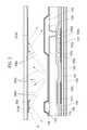
- FIG 1 is a view showing the configuration of a display device to which one embodiment of the present invention is applied.
- a display device of FIG 1 may include, but is not limited to, an organic light emitting display panel as a display panel 11.
- the present invention may be applied to an organic light emitting display panel of either a top surface emission type or a bottom surface emission type.
- a display device 100 includes a display panel 11 having a plurality of first lines VL1 to VLm formed, or located, in a first direction (for example, a vertical direction) and a plurality of second lines HL1 to HLn formed, or located, in a second direction (for example, a horizontal direction), a first driver 12 for applying a first signal to the plurality of first lines VL1 to Vlm, a second driver 13 for applying a second signal to the plurality of second lines HL1 to HLn, a timing controller 14 for controlling the first driver 12 and the second driver 13, etc.
- the display panel 11 has a plurality of pixels defined at intersections of the plurality of first lines VL1 to VLm formed, or located, in the first direction (for example, the vertical direction) and the plurality of second lines HL1 to HLn formed, or located, in the second direction (for example, the horizontal direction).
- Each of the first and second drivers 12 and 13 may include at least one driver IC which outputs a signal for displaying an image.
- the plurality of first lines VL1 to VLm formed, or located, in the first direction in the display panel 11 may be, for example, data lines which are formed, or located, in the vertical direction (the first direction) and transfer a data voltage (the first signal) to a pixel column in the vertical direction.
- the first driver 12 may be a data driver for applying the data voltage to the data lines.
- the plurality of second lines HL1 to HLn formed, or located, in the second direction in the display panel 11 may be gate lines which are formed, or located, in the horizontal direction (the second direction) and transfer a scan signal (the second signal) to the pixel column in the horizontal direction.
- the second driver 13 may be a scan driver for applying the scan signal to the gate lines.
- the display panel 11 may include a pad part (not shown) used to interconnect the first driver 12 and the second driver 13.
- the pad part transfers the first signal to the display panel 11.
- the pad part transfers the second signal to the display panel 11.
- Each of the pixels includes one or more subpixels.
- a subpixel used herein refers to a unit to allow an organic light emitting element to emit light of a particular color through a certain kind of color filter formed, or located, therein or without any color filter. Colors defined in the subpixel may include, but is not limited to, red (R), green (G), blue (B) and optionally white (W).
- Each subpixel includes a separate thin film transistor and an electrode connected thereto. Therefore, in the following description, subpixels constituting a pixel will be collectively referred to as one pixel region. That is, a group of subpixels may constitute a pixel. For convenience, subpixels will be referred to as a pixel.
- FIG 2 is a sectional view showing the configuration of an organic light emitting display panel with a mirror function.
- FIG 2 is also a sectional view of a pixel of the mirror display panel.
- a buffer 101 On a first substrate 100 are arranged a buffer 101, an active layer 102a, conductive portions 102s and 102d formed, or located, in both sides of the active layer 102a, a gate 107, a gate insulating film 103 formed, or located, between the gate 107 and the active layer 102a, a source 105s, a drain 105d, a first electrode 120 for controlling emission for each pixel, a second electrode 150 disposed over a plurality of pixels, and a bank 130 defining an emission region.
- an organic light emitting layer 140 is interposed between the first electrode 120 and the second electrode 150 and may also be disposed on the bank 130.
- two layers 107c and 102c for a storage capacitor are disposed.
- the pixel structure of FIG 2 is just illustrative but the pixel may have different structures, for example, a TFT structure, without being limited thereto.
- mirrors 210a and 210b for reflecting external light are arranged on a second substrate 200. Due to a distance between the mirrors 210a and 210b and the organic light emitting layer 140 of the first substrate 100, some 290a of light emitted from the organic light emitting layer 140 travels upward, whereas some 290b and 290c is totally reflected toward an edge, which may result in reduction of luminance efficiency.
- FIG 3 is a sectional view showing the configuration of an organic light emitting display panel with a transmission function.
- FIG. 3 is also a sectional view of a pixel of the transmission display panel.
- a color filter 350 is arranged on a second substrate 200. Due to a distance between the second substrate 200 and an organic light emitting layer 140 of a first substrate 100, some 390a of light emitted from the organic light emitting layer 140 travels upward, whereas some 390b and 390c is totally reflected toward an edge, which may result in reduction of luminance efficiency.
- the display panel with the mirror function or the transmission function has reduced luminance efficiency since some light is totally reflected toward the edge due to a top plate bonding structure. Therefore, there is a need of a structure allowing light to be output externally in a display panel with the transmission function or the mirror function.
- the display panel includes a first substrate having a pixel region and an emission region which are defined by a plurality of gate lines and a plurality of data lines, and a second substrate on which a partition is disposed.
- the partition of the second substrate in the display panel has a reversed taper structure.
- a display panel and a display device include a structure in which two substrates are bonded to face with each other.
- a display panel may be an organic light emitting display panel or an organic light emitting display device, or a liquid crystal display panel or a liquid crystal display device.
- the present invention is not limited thereto but may be applied to different display devices and display panels with a transmission or mirror function.
- the common structure of the display panel of the present invention is a structure including a first substrate or lower substrate formed, or located, thereon with thin film transistors for controlling pixels and gate lines and data lines connected to the thin film transistors, and an opposing second substrate or upper substrate on which a partition is arranged.
- the present invention can be applied to a mirror display device or a transmission display device and can improve luminance efficiency of these display devices.
- a low refractive index reversed taper structure formed, or located, on the second substrate or upper substrate is referred to as a partition.
- the partition is disposed to correspond to an emission region or pixel region of the first substrate (lower substrate).
- the partition may be formed of a negative photoresist.
- the negative photoresist is deposited (coated) and developed, it is possible to form a reversed taper structure and control a range of luminance viewing angle depending on an angle of taper.
- the present invention is not necessarily limited to the negative photoresist but may employ different materials as long as they can be used to form a reverse tapered partition in order to implement the display device or display panel of the present invention.
- the present invention is not necessarily limited to the reverse taper structure.
- the present invention may involve forming a partition with a low refractive index material and include all partition structures in which light emitted from an emission region by control of TFTs formed in a pixel region is guided to be reflected toward the upper substrate (the second substrate) by the partition.
- the second substrate is bonded to a first substrate to form the display panel 11.
- the first substrate is formed, or located, thereon with a plurality of gate lines to which a gate signal is applied, a plurality of data lines to which a data signal is applied, a plurality of pixels defined at intersections of the data lines and the data lines, and a bank defining a pixel emission region.
- the second substrate has a partition formed, or located, to correspond to the bank region.
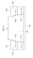
- FIG 4 is a sectional view of a substrate on which partitions are formed, or located, according to one embodiment of the present invention.
- Each of partitions formed, or located, on the second substrate i.e., an upper substrate
- a reverse taper structure may be considered to be any structure with an associated width that increases as the distance from the second substrate is increased.
- partitions 410a and 410b are formed, or located, on an upper substrate, i.e., the second substrate 200.
- An emitting area (EA) in which the partitions 410a and 410b are not formed, or located, corresponds to an emission area in a pixel region.
- the emission area may be considered to be the area from which light is emitted.
- the EA emits light when an organic layer emits light according to pixel control.
- a material of which the partitions 410a and 410b are made has a lower refractive index than a material formed, or located, in a region 490 where light is emitted and transmitted.
- the partitions 410a and 410b cause the light generated due to the emission of the organic layer to be travelled to the second substrate (i.e., the upper substrate 200) without being totally reflected toward an edge.
- the partitions 410a and 410b can be deposited and formed by using a material having a smaller refractive index than the adhesive material. Accordingly, since the refractive index of the partitions 410a and 410b is smaller than a material (for example, air, vacuum or the others) of the emission area, the partitions 410a and 410b can reflect the light to be travelled toward the second substrate, which may result in improvement of luminance efficiency.
- An angle Arc_A formed between a section (substrate side section) where the partitions 410a and 410b are in contact and a side wall of the partitions 410a and 410b may be equal to or greater than 90 degrees.
- light propagating at a low angle can also be output in front.
- the partitions tapered reversely with respect to the second substrate can prevent light between banks from being laterally totally reflected, which can result in increase in the output (luminance) efficiency of light emitted from the organic layer.
- reference numeral 415a denotes a bank side section of the partition 410a
- reference numeral 415b denotes a bank side section of the partition 410b.
- the bank side sections 415a and 415b may or not contact a bank of the lower substrate.
- an adhesive material may be coated on the bank side sections 415a and 415b so as to maintain a state of adhesion between the upper substrate and the lower substrate.
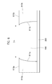
- FIG 5 is a sectional view of a substrate on which partitions are formed, or located, according to another embodiment of the present invention, in which a lateral side of each partition has a concave polygonal surface.
- each of partitions 510a and 510b formed, or located, on the second substrate 200 is not flat.
- the partition 510a has a concave polygonal surface combining two faces 511 a and 512a.
- An angle Arc_B formed between the face 511a and the substrate side section of the partition may be made to be smaller than an angle Arc_C formed between the face 512a and a face parallel to the substrate side section of the partition. This can increase the light output efficiency.
- the other partition 510b has a concave polygonal surface combining two faces 511 band 512b.
- the partitions After depositing a material (for example, a negative photoresist) used to form the partitions to provide the structure as shown in FIG 5 on the second substrate (i.e., the upper substrate 200), when the material is exposed or etched using a halftone mask, the partitions can have a two-step reversed taper structure by adjusting exposure time or exposure amount.
- a material for example, a negative photoresist
- FIG 5 shows the section of the second substrate on which the partitions having the two-step reversed taper structure are formed, or located, the present invention is not limited thereto.
- the partitions may have a three or more-step reverse taper structure, which falls within the scope of the invention defined in the claims.
- bank side sections 515a and 515b may or may not contact a bank of the lower substrate.
- an adhesive material may be coated on the bank side sections 515a and 515b so as to maintain a state of adhesion between the upper substrate and the lower substrate.
- the partitions 510a and 510b can be deposited and formed by using a material having a smaller refractive index than the adhesive material.
- a material having a lower refractive index than a material for example, air, vacuum or the others
- FIG 6 is a sectional view of a substrate on which partitions are formed, or located, according to still another embodiment of the present invention, in which a lateral side of each partition has a concave arc-shaped surface.
- each of partitions 610a and 610b formed, or located, on the second substrate 200 is not flat.
- the partition 610a has a concave arc-shaped surface 611a.
- the partition 610b has a concave arc-shaped surface 611b.
- the partitions After depositing a material (for example, a negative photoresist) used to form the partitions to provide the structure as shown in FIG. 6 on the second substrate (i.e., the upper substrate 200), when the material is exposed or etched using a halftone mask, the partitions can have a concave reversed taper structure by gradually increasing exposure time or exposure amount.
- a material for example, a negative photoresist
- FIG. 6 shows the section of the second substrate on which the partitions having the concave reversed taper structure are formed, or located
- the present invention is not limited thereto.
- the partitions may have a combination of the structure of FIG 5 and the structure of FIG. 6 , which falls within the scope of the invention defined in the claims.
- the partitions may have a reversed taper structure including a linear face and an arc-shape face.
- bank side sections 615a and 615b may or not contact a bank of the lower substrate.
- an adhesive material may be coated on the bank side sections 615a and 615b so as to maintain a state of adhesion between the upper substrate and the lower substrate.
- the partitions 610a and 610b can be deposited and formed by using a material having a smaller refractive index than the adhesive material.
- a material having a lower refractive index than a material for example, air, vacuum or the others
- the partitions shown in FIGS. 4 to 6 can have a smaller refractive index than the material formed, or located, in the regions 490, 590 and 690 where the light is emitted and transmitted.
- a low refractive index organic film may be used to form the partitions.
- the organic film may have a refractive index smaller than 1.53 (i.e., n ⁇ 1.53).
- a separate reflective material may be formed, or located, on a lateral side of each of the partitions shown in FIGS. 4 to 6 , thereby further improving the light output efficiency.
- a separate reflective material may be formed, or located, on a lateral side of each of the partitions shown in FIGS. 4 to 6 , thereby further improving the light output efficiency.
- partitions are formed, or located, on an extension surface of a mirror, it is possible to improve the output efficiency of light emitted from an organic layer without impairing visibility.
- FIG 7 is a view showing the configuration of a display panel according to one embodiment of the present invention.
- the first substrate 100, the thin film transistors, the data lines and the gate lines and so on, which are formed, or located, on the first substrate 100, have the same configurations as described above and, therefore, explanation of which will not repeated for the purpose of brevity.
- Partitions 710a and 710b are formed, or located, in a region corresponding to the bank 130.
- An adhesive material such as a resin may be formed, or located, in a region 790.
- a refractive index of the partitions 710a and 710b may be smaller than that of the adhesive material in the region 790.
- the display panel of FIG 7 becomes a transparent display panel when the data lines, the data lines, the thin film transistors, the first electrode, the second electrode and so on formed, or located, on the lower substrate are made of a transparent material.
- the color filter 350 can be used to decrease reflection of wirings and haze and the inversed tapered partitions 710a and 710b formed, or located, in the vicinity of the emission are can be used to increase the light output efficiency.
- the color filter 350 is interposed between the partitions 710a and 710b in correspondence to the emission area and is set to be lower than or flush with the partitions 710a and 710b.
- the transparent display panel includes gate lines and data lines made of a transparent conductive material and can be fabricated by selecting a material of the partitions such that the light transmittance of the partitions corresponding to the bank region is equal to or greater than the light transmittance of the first substrate.
- the transparent display panel since external light can pass through the partitions, it is possible to fabricate the transparent display panel.
- FIG 8 is a view showing the configuration of a mirror display panel according to another embodiment of the present invention.
- the first substrate 100, the thin film transistors, the data lines and the gate lines and so on, which are formed, or located, on the first substrate 100, have the same configurations as described above and, therefore, explanation of which will not repeated for the purpose of brevity.
- Partitions 810a and 810b are formed, or located, in a region corresponding to the bank 130. As shown in FIG 8 , the partitions 810a and 810b may be formed, or located, on mirrors 210a and 210b, respectively. An adhesive material such as a resin may be formed, or located, in a region 890. A refractive index of the partitions 810a and 810b may be smaller than that of the adhesive material in the region 890.
- the reverse tapered partitions 810a and 810b can be formed in an exposure manner by patterning the mirrors 210a and 210b by sputtering, exposing and etching metal having a high reflectivity in compliance with the emission area 890, and then coating a high refractive index organic film thereon.
- a negative photoresist may also be used without being limited thereto.
- a separate reflective material may be formed, or located, on a lateral side of each of the partitions 810a and 810b shown in FIG 8 , thereby further improving the light output efficiency.
- a separate reflective material may be formed, or located, on a lateral side of each of the partitions 810a and 810b shown in FIG 8 , thereby further improving the light output efficiency.
- partitions are formed, or located, on extension surfaces of mirrors, it is possible to improve the output efficiency of light emitted from the organic layer without impairing visibility.
- the partitions shown in FIGS. 7 and 8 are examples of the partitions shown in FIG 4 .
- the present invention is not limited thereto.
- the partitions having the concave polygonal surfaces or the concave arc-shaped surface shown in FIGS. 5 and 6 may be applied to the structures shown in FIGS. 7 and 8 .
- the color filter 350 shown in FIG 7 may also be formed as shown in FIG 8 .
- the color filter 350 shown in FIG 7 is interposed between the partitions 810a and 810b in correspondence to the emission area and is lower than or flush with the partitions 810a and 810b.
- FIG 9 is a view showing a relationship between a reverse taper angle of partitions according to one embodiment of the present invention and a viewing angle.
- a comparison can be made between a mirror display panel 901 and a mirror display panel 902 in terms of a total aperture ratio of a highly-reflective metal material constituting a mirror and a reverse taper angle of partitions.
- metal mirrors 210c and 210d are formed and an angle formed between partitions 910a and 910b and the second substrate 200 or the mirrors 210c and 210d is denoted by Arc_D.
- metal mirrors 210e and 210f are formed and an angle formed between partitions 910c and 910d and the second substrate 200 or the mirrors 210e and 210f is denoted by Arc_E.
- the aperture ratio of the metal constituting the mirrors 210c and 210d of the mirror display panel 901 is lower than the aperture ratio of the metal constituting the mirrors 210e and 210f of the mirror display panel 902.
- the reverse taper angle Arc_D of the mirror display panel 901 is smaller than the reverse taper angle Arc_E of the mirror display panel 902.
- the reverse taper angle of the partitions can be decreased for the narrow viewing angle. To this end, exposure time and exposure amount can be adjusted.
- the reverse taper angle of the partitions can be decreased for the wide viewing angle.
- exposure time and exposure amount can be adjusted.
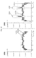
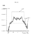
- FIG 10 is a view showing a degree of improvement of luminance efficiency when a reverse tapered low refractive index organic film according to one embodiment of the present invention is used to form partitions. As one example, a result of simulation for a mirror display device will be described below.
- a graph 1001 shows a change in vertical viewing angle 1001v and horizontal viewing angle 1001h in the display panel structure as shown in FIG 2 .
- a graph 1002 shows a change in vertical viewing angle 1002v and horizontal viewing angle 1002h in the display panel structure as shown in FIG 8 . It can be seen from the graph 1002 that luminance is increased by about 4.8% near a one side viewing angle of 40 degrees (in a range from 37 degrees to 43 degrees) (see reference numerals 1010 and 1020).
- FIG 11 is a view showing a degree of improvement of luminance efficiency when a two-step reverse tapered low refractive index organic film according to another embodiment of the present invention is used to form partitions.
- a result of simulation for a mirror display device with the partitions shown in FIG 4 will be described below.
- the vertical viewing angle 1101v and the horizontal viewing angle 1101h are both increased (see reference numeral 1120).
- FIG 12 is a view showing the configuration of partitions according to another embodiment of the present invention.
- the partitions are formed, or located, on the second substrate corresponding to a bank region but may not be necessarily formed, or located, in the entire bank region.
- a bank 1230 is formed, or located, between two emission areas 1291 and 1292 to define pixel regions or the emission areas 1291 and 1292.
- the partitions 1210a and 1210b facing the bank 1230 may be formed, or located, on the second substrate 200 in alignment with a boundary of the bank 1230.
- a separate material may not be formed, or located, or an adhesive material for bonding may be formed, or located. This can help to increase the luminance efficiency of light emitted from the emission areas and a force of adhesion of the display panel to the substrate.
- a method of fabricating the display panel as described above includes a step of forming a bank defining an emission area on a first substrate, and a step of forming partitions in a region of a second substrate. This method further includes a step of forming the partitions formed on the second substrate such that the partitions have a reverse taper structure. In addition, this method further includes a step of coating and exposing a negative photoresist in order to form reverse tapered partitions on the second substrate in the display panel.
- FIG 13 is a view showing a process of fabricating a display panel according to one embodiment of the present invention.
- a plurality of gate lines are formed, or located, to which a gate signal is applied, a plurality of data lines to which a data signal is applied, a plurality of pixels defined at intersections of the gate lines and data lines, and a bank region defining an emission area (S1310).
- reverse tapered partitions are formed, or located, on a second substrate to be bonded with the first substrate (S1320).
- the partitions corresponding to the bank region may be formed, or located, to correspond to the entire bank region, as described above with reference to FIGS. 3 to 8 , or may be formed, or located, to correspond to an edge of the bank region, as described above with reference to FIG.12 .
- the two substrates (the first and second substrates) are bonded together (S1330).
- a low refractive index reverse taper structure may be formed.
- the low refractive index reverse taper structure is one example of the partitions.
- a low refractive reverse taper structure can be formed after color filters corresponding to RGB and a black matrix are formed, or located.
- the low refractive index reverse taper structure is one example of the partitions.
- the refractive index of the partitions is lower than the refractive index of a material interposed between the emission area and the second substrate.
- a low refractive index organic film may be used to form the partitions.
- the two substrates can be bonded together by forming, or locating, an adhesive material in a region in the second substrate where no partition is formed, or located.
- an adhesive material may be formed, or located, in the emission area.
- the refractive index of the partitions is set to be lower than the refractive index of the adhesive material.
- the refractive index of the adhesive material may be higher than the refractive material of the partitions.
- the refractive indexes of the partitions and the adhesive material may be independent of each other.
- FIG 14 is a view for explaining the partition forming process according to one embodiment of the present invention in more detail.
- a negative photoresist is deposited on the second substrate (S1321) and a photomask corresponding to the bank region of the first substrate is used to expose the negative photoresist, thereby forming the partitions (S1322). Since the negative photoresist is cured when receiving light, the partitions can have the reverse tapered lateral side shown in FIGS. 4 , 5 and 6 . In addition, a baking process of curing the exposed negative photoresist may be selectively performed to maintain the shape of the reverse tapered partitions (S1323).
- a halftone photomask or a multi-tone photomask may be used to form the lateral side of the partitions in a concave polygonal shape or a concave arc shape. It has been illustrated in FIG 11 that the concave polygonal shape or the concave arc shape provides the increased luminance efficiency.
- Exposure time or exposure amount may be adjusted to form the lateral side of the partitions in a concave polygonal shape or a concave arc shape.
- the photomask used in the bank forming process may be used as it is without a separate halftone photomask or multi-tone photo mask, which can result in reduction of costs of process and production.
- a low refractive index reverse taper structure can be formed, or located, on the second substrate (or the upper substrate) in compliance with the emission area of the first substrate (or the lower substrate).
- the low refractive index reverse taper structure is one example of the partitions used to increase the luminance efficiency.
- a reverse taper structure can be formed and a desired luminance viewing angle range can be controlled depending on a taper angle.
- a desired luminance viewing angle range can be controlled depending on a taper angle.
- the organic film can have a thickness such that it is in maximum contact with the bank of the lower substrate and the bank can be formed by a material absorbing light such that light emitted from each light source is totally reflected at a low refractive index film.
- a space may be formed, or located, between the bank and the partitions.
- the luminance efficiency can be further improved by coating a reflective material on the lateral side of the partitions.
- a process of forming, or locating, a color filter which is lower than or flush with the partitions, in a region corresponding to the emission area, may be added. This can be applied to a display device including a color filter.
- a sequence of processes of forming partitions and color filters can be determined in various ways.
- the present invention can implement a display panel and a display device which are capable of improving the luminance efficiency of a mirror display panel or a transmission display panel.
- the present invention can implement a display panel and a display device which is capable of outputting light emitted from an emission area outside the display panel without being reflected by a mirror.
- partitions can be formed by a photomask used to form a bank, it is possible to fabricate a display panel and a display device without employing a separate photomask. That is, since the partitions can be exposed by using the photomask used to form the bank, a need to form a separate photomask is eliminated, which can result in reduction of production costs.
- a viewing angle of a display panel it is possible to adjust a viewing angle of a display panel by forming the first substrate in the same way and forming partitions of the second substrate in various ways.
- a display panel is classified into three types depending on a viewing angle.
- a second substrate for the narrow viewing angle for fabricating the narrow viewing angle display panel, a second substrate for the middle viewing angle, and a second substrate for the wide viewing angle can be separately formed, while forming a first substrate in common.
- This allows a reverse taper angle of partitions to be adjusted, as shown in FIG 9 .
Landscapes
- Engineering & Computer Science (AREA)
- Physics & Mathematics (AREA)
- Optics & Photonics (AREA)
- Microelectronics & Electronic Packaging (AREA)
- Computer Hardware Design (AREA)
- General Physics & Mathematics (AREA)
- Theoretical Computer Science (AREA)
- Manufacturing & Machinery (AREA)
- Electroluminescent Light Sources (AREA)
- Optical Filters (AREA)
- Devices For Indicating Variable Information By Combining Individual Elements (AREA)
Abstract

Description
- The present invention relates to a display panel with luminance efficiency improvement, a display device, and a method of fabricating the display panel.
- A display device is a device for visually displaying data, such as a liquid crystal display, an electrophoretic display, an organic light emitting display, an inorganic electroluminescent (EL) display, an electroluminescent display, a field emission display, a surface conduction electron emitter display, a plasma display, a cathode ray display and the like.
- Among these displays, the organic light emitting display is a display including two different electrodes and an emission layer interposed therebetween. In this display, when electrons generated in one electrode and holes generated in the other electrodes are injected into the emission layer, the injected electrons and holes are combined to generate excitons. While the generated excitons are falling from an excited state to a ground state, light is emitted from the emission layer, thereby displaying an image.
- Some display devices can provide a mirror function or a transmission function. The mirror function refers to a function to reflect external light by a reflective material formed, or located, in a display panel. The transmission function refers to a function to transmit external light through a display panel.
- However, such a mirror function or transmission function may deteriorate luminance efficiency of light emitted from pixels of the display panel. Therefore, there is a need of a display panel and a display device which are capable of improving the luminance efficiency.
- The present disclosure provides a display panel and a display device which are capable of improving luminance efficiency of a mirror display panel or a transmission display panel, and a method for fabricating the display panel.
- In addition, the present disclosure provides a display panel and a display device which are capable of outputting light emitted from an emission area outside the display panel without being reflected by a mirror, and a method for fabricating the display panel.
- In addition, the present disclosure provides a display panel and a display device which are capable of outputting light emitted from an emission area outside the display panel without being totally reflected at an upper substrate, and a method for fabricating the display panel.
- In addition, the present disclosure provides a display panel and a display device which are capable of specifically adjusting a viewing angle of light emitted from an emission area, and a method for fabricating the display panel.
- The present invention provides a display panel comprising: a first substrate on which a plurality of gate lines, a plurality of data lines, a plurality of pixels and a bank defining an emission area of the pixels are formed, or located,; and a second substrate on which partitions are formed, or located, in correspondence to a region where the bank is formed, or located,, wherein a refractive index of the partitions is lower than a refractive index of a material interposed between the emission area and the second substrate.
- The partitions formed, or located, on the second substrate are formed, or located, in correspondence to a region where the bank is formed, or located. In other words, the partitions and the bank may be formed, or located, such that the partitions and the bank define a space between the emission area and the second substrate, and the material interposed between the emission area and the second substrate is in the space. The partitions and the bank may at least partially define the space between the emission area and the second substrate.
- According to the present invention, there is provided a display panel including: a first substrate with pixel areas and emission areas which are defined by a plurality of gate lines and a plurality of data lines; and a second substrate on which partitions are formed, or located.
- Partitions of the second substrate may have a reverse taper structure.
- Partitions of the second substrate may have a multi-step reverse taper shape or a concave groove shape.
- According to another embodiment of the present invention, there is provided a display device having a structure which is capable of outputting light emitted from an emission area outside a display panel by means of partitions.
- The display device may include a display panel on which a reflective material and partitions are formed, or located.
- The display device may include a display panel having a substrate on which partitions having a reverse tapered structure are formed, or located, and a transparent substrate.
- According to another embodiment of the present invention, there is provided a method for fabricating a display panel, including forming, or locating, a bank defining an emission area on a first substrate; and forming, or locating, partitions on a second substrate in a region corresponding to the bank. In this way, the partitions and the bank may define a space between the emission area and the second substrate, as described herein.
- The method may further include forming the partitions such that the partitions have a reverse tapered structure.
- The method may further include coating a negative photoresist on the second substrate and then forming reverse tapered partitions by exposing the coated negative photoresist.
- The present invention can implement a display panel and a display device which are capable of improving the luminance efficiency of a mirror display panel or a transmission display panel.
- In addition, the present invention can implement a display panel and a display device which are capable of outputting light emitted from an emission area outside the display panel without being reflected by a mirror.
- In addition, according to the present invention, since partitions can be formed by using a photomask used to form partitions, it is possible to fabricate a display panel and a display device without a separate photomask.
-
-
FIG 1 is a view showing the configuration of a display device to which one embodiment of the present invention is applied. -
FIG 2 is a sectional view showing the configuration of an organic light emitting display panel with a mirror function. -
FIG 3 is a sectional view showing the configuration of an organic light emitting display panel with a transmission function. -
FIG. 4 is a sectional view of a substrate on which partitions are formed, or located, according to one embodiment of the present invention. -
FIG. 5 is a sectional view of a substrate on which partitions are formed, or located, according to another embodiment of the present invention. -
FIG 6 is a sectional view of a substrate on which partitions are formed, or located, according to still another embodiment of the present invention. -
FIG 7 is a view showing the configuration of a display panel according to one embodiment of the present invention. -
FIG 8 is a view showing the configuration of a mirror display panel according to another embodiment of the present invention. -
FIG 9 is a view showing a relationship between a reverse taper angle of partitions according to one embodiment of the present invention and a viewing angle. -
FIG 10 is a view showing a degree of improvement of luminance efficiency when a reverse tapered low refractive index organic film according to one embodiment of the present invention is used to form partitions. -
FIG 11 is a view showing a degree of improvement of luminance efficiency when a two-step reverse tapered low refractive index organic film according to another embodiment of the present invention is used to form partitions. -
FIG 12 is a view showing the configuration of partitions according to another embodiment of the present invention. -
FIG 13 is a view showing a process of fabricating a display panel according to one embodiment of the present invention. -
FIG 14 is a view for explaining a partition forming process according to one embodiment of the present invention in more detail. - The above objects, features and advantages will become more clearly apparent from the following detailed description in conjunction with the accompanying drawings. Therefore, the technical ideas of the present invention can be easily understood and practiced by those skilled in the art.
- In the following detailed description of the present invention, concrete description on related functions or constructions will be omitted if it is deemed that the functions and/or constructions may hinder the understanding of the present invention. Hereinafter, preferred embodiments of the present invention will be described in detail with reference to the accompanying drawings. Throughout the drawings, the same or similar elements are denoted by the same reference numerals. In the present specification, a detailed description of well-known functions and configurations will be omitted so as not to make the scope of the present invention unclear.
- In the following description, the term "upper portion (or lower portion)" or "upper (or lower)" refers to not only including or forming a certain configuration in contact with an upper surface (or lower surface) of a base but also including or forming other configurations between the certain configuration and the base or below the base. In addition, in the following description, the terms "first," "second," "A," "B," "(a)," "(b)," " and so on are just used to distinguish one element from another but are not intended to limit the essence, sequence, order or number of elements. When a certain element is "connected," "coupled" or "contacted" to another, it is to be understood that the certain element may be "connected," "coupled" or "contacted" to another directly or via a different element. A reverse taper may be any taper that results in an overhanging structure.
- A display device of the present invention outputs external input image data by using a variety of light sources. In this course, the image data are divided into R (red), G (green), B (blue), and selectively W (white) or black to be provided to the display device. The display device may provide other functions, rather than providing the image data. In particular, when the display device further includes a function of sensing light, it is possible to adjust image luminance or color balance of images output depending on a magnitude of external light.
-
FIG 1 is a view showing the configuration of a display device to which one embodiment of the present invention is applied. A display device ofFIG 1 may include, but is not limited to, an organic light emitting display panel as adisplay panel 11. The present invention may be applied to an organic light emitting display panel of either a top surface emission type or a bottom surface emission type. - Referring to
FIG 1 , adisplay device 100 includes adisplay panel 11 having a plurality of first lines VL1 to VLm formed, or located, in a first direction (for example, a vertical direction) and a plurality of second lines HL1 to HLn formed, or located, in a second direction (for example, a horizontal direction), afirst driver 12 for applying a first signal to the plurality of first lines VL1 to Vlm, asecond driver 13 for applying a second signal to the plurality of second lines HL1 to HLn, atiming controller 14 for controlling thefirst driver 12 and thesecond driver 13, etc. - The
display panel 11 has a plurality of pixels defined at intersections of the plurality of first lines VL1 to VLm formed, or located, in the first direction (for example, the vertical direction) and the plurality of second lines HL1 to HLn formed, or located, in the second direction (for example, the horizontal direction). - Each of the first and
second drivers - The plurality of first lines VL1 to VLm formed, or located, in the first direction in the
display panel 11 may be, for example, data lines which are formed, or located, in the vertical direction (the first direction) and transfer a data voltage (the first signal) to a pixel column in the vertical direction. Thefirst driver 12 may be a data driver for applying the data voltage to the data lines. - The plurality of second lines HL1 to HLn formed, or located, in the second direction in the
display panel 11 may be gate lines which are formed, or located, in the horizontal direction (the second direction) and transfer a scan signal (the second signal) to the pixel column in the horizontal direction. Thesecond driver 13 may be a scan driver for applying the scan signal to the gate lines. - The
display panel 11 may include a pad part (not shown) used to interconnect thefirst driver 12 and thesecond driver 13. When the first signal is applied from thefirst driver 12 to the plurality of first lines VL1 to VLm, the pad part transfers the first signal to thedisplay panel 11. Similarly, when the second signal is applied from thesecond driver 13 to the plurality of second lines HL1 to HLn, the pad part transfers the second signal to thedisplay panel 11. - Each of the pixels includes one or more subpixels. A subpixel used herein refers to a unit to allow an organic light emitting element to emit light of a particular color through a certain kind of color filter formed, or located, therein or without any color filter. Colors defined in the subpixel may include, but is not limited to, red (R), green (G), blue (B) and optionally white (W). Each subpixel includes a separate thin film transistor and an electrode connected thereto. Therefore, in the following description, subpixels constituting a pixel will be collectively referred to as one pixel region. That is, a group of subpixels may constitute a pixel. For convenience, subpixels will be referred to as a pixel.
-
FIG 2 is a sectional view showing the configuration of an organic light emitting display panel with a mirror function.FIG 2 is also a sectional view of a pixel of the mirror display panel. - As shown in
FIG 2 , on afirst substrate 100 are arranged abuffer 101, anactive layer 102a,conductive portions active layer 102a, agate 107, agate insulating film 103 formed, or located, between thegate 107 and theactive layer 102a, asource 105s, adrain 105d, afirst electrode 120 for controlling emission for each pixel, asecond electrode 150 disposed over a plurality of pixels, and abank 130 defining an emission region. In addition, an organiclight emitting layer 140 is interposed between thefirst electrode 120 and thesecond electrode 150 and may also be disposed on thebank 130. In addition, twolayers - The pixel structure of
FIG 2 is just illustrative but the pixel may have different structures, for example, a TFT structure, without being limited thereto. - As shown in
FIG 2 , mirrors 210a and 210b for reflecting external light are arranged on asecond substrate 200. Due to a distance between themirrors light emitting layer 140 of thefirst substrate 100, some 290a of light emitted from the organiclight emitting layer 140 travels upward, whereas some 290b and 290c is totally reflected toward an edge, which may result in reduction of luminance efficiency. -
FIG 3 is a sectional view showing the configuration of an organic light emitting display panel with a transmission function.FIG. 3 is also a sectional view of a pixel of the transmission display panel. - As shown in
FIG 3 , acolor filter 350 is arranged on asecond substrate 200. Due to a distance between thesecond substrate 200 and an organiclight emitting layer 140 of afirst substrate 100, some 390a of light emitted from the organiclight emitting layer 140 travels upward, whereas some 390b and 390c is totally reflected toward an edge, which may result in reduction of luminance efficiency. - As described with reference to
FIGS. 2 and3 , the display panel with the mirror function or the transmission function has reduced luminance efficiency since some light is totally reflected toward the edge due to a top plate bonding structure. Therefore, there is a need of a structure allowing light to be output externally in a display panel with the transmission function or the mirror function. - Hereinafter, a display panel and a display device which are capable of improving luminance efficiency by using a low refractive reversed taper structure will be described. The display panel includes a first substrate having a pixel region and an emission region which are defined by a plurality of gate lines and a plurality of data lines, and a second substrate on which a partition is disposed. The partition of the second substrate in the display panel has a reversed taper structure. When implementing a mirror display device, the present invention involves a display panel in which a partition is arranged on a substrate on which a reflector is formed, or located.
- A display panel and a display device include a structure in which two substrates are bonded to face with each other. A display panel may be an organic light emitting display panel or an organic light emitting display device, or a liquid crystal display panel or a liquid crystal display device. However, the present invention is not limited thereto but may be applied to different display devices and display panels with a transmission or mirror function. The common structure of the display panel of the present invention is a structure including a first substrate or lower substrate formed, or located, thereon with thin film transistors for controlling pixels and gate lines and data lines connected to the thin film transistors, and an opposing second substrate or upper substrate on which a partition is arranged. In particular, the present invention can be applied to a mirror display device or a transmission display device and can improve luminance efficiency of these display devices.
- Hereinafter, a low refractive index reversed taper structure formed, or located, on the second substrate or upper substrate is referred to as a partition. The partition is disposed to correspond to an emission region or pixel region of the first substrate (lower substrate). The partition may be formed of a negative photoresist. When the negative photoresist is deposited (coated) and developed, it is possible to form a reversed taper structure and control a range of luminance viewing angle depending on an angle of taper. Of course, the present invention is not necessarily limited to the negative photoresist but may employ different materials as long as they can be used to form a reverse tapered partition in order to implement the display device or display panel of the present invention.
- In addition, the present invention is not necessarily limited to the reverse taper structure. The present invention may involve forming a partition with a low refractive index material and include all partition structures in which light emitted from an emission region by control of TFTs formed in a pixel region is guided to be reflected toward the upper substrate (the second substrate) by the partition.
- Hereinafter, a second substrate constituting the
display panel 11 shown inFIG. 1 will be described. More specifically, the second substrate is bonded to a first substrate to form thedisplay panel 11. The first substrate is formed, or located, thereon with a plurality of gate lines to which a gate signal is applied, a plurality of data lines to which a data signal is applied, a plurality of pixels defined at intersections of the data lines and the data lines, and a bank defining a pixel emission region. The second substrate has a partition formed, or located, to correspond to the bank region. -
FIG 4 is a sectional view of a substrate on which partitions are formed, or located, according to one embodiment of the present invention. Each of partitions formed, or located, on the second substrate (i.e., an upper substrate) has a reverse taper structure. A reverse taper structure may be considered to be any structure with an associated width that increases as the distance from the second substrate is increased. For example, as shown inFIG 4 ,partitions second substrate 200. An emitting area (EA) in which thepartitions partitions region 490 where light is emitted and transmitted. As a result, thepartitions - If the material formed, or located, in the
region 490 where light is emitted and transmitted is an adhesive material for bonding the upper substrate and the lower substrate together, thepartitions partitions partitions - In particular, it is possible to control the luminance efficiency by selecting an adhesive material which has a larger refractive index than the partitions and bonds the first substrate and the second substrate together in the emission area. This can be verified in a process of light emission due to a refractive index difference in a propagation direction of light 791a and 791b (see
FIG. 7 which will be described later). - An angle Arc_A formed between a section (substrate side section) where the
partitions partitions - A section facing a bank portion of the first substrate (i.e., the lower substrate) in the
partitions FIG 4 ,reference numeral 415a denotes a bank side section of thepartition 410a and reference numeral 415b denotes a bank side section of thepartition 410b. Thebank side sections bank side sections -
FIG 5 is a sectional view of a substrate on which partitions are formed, or located, according to another embodiment of the present invention, in which a lateral side of each partition has a concave polygonal surface. - As shown in
FIG 5 , the lateral side of each ofpartitions second substrate 200 is not flat. Referring to thepartition 510a, thepartition 510a has a concave polygonal surface combining twofaces - An angle Arc_B formed between the
face 511a and the substrate side section of the partition may be made to be smaller than an angle Arc_C formed between theface 512a and a face parallel to the substrate side section of the partition. This can increase the light output efficiency. - Similarly, the
other partition 510b has a concave polygonal surface combining two faces 511band 512b. - After depositing a material (for example, a negative photoresist) used to form the partitions to provide the structure as shown in
FIG 5 on the second substrate (i.e., the upper substrate 200), when the material is exposed or etched using a halftone mask, the partitions can have a two-step reversed taper structure by adjusting exposure time or exposure amount. - Although
FIG 5 shows the section of the second substrate on which the partitions having the two-step reversed taper structure are formed, or located, the present invention is not limited thereto. For example, the partitions may have a three or more-step reverse taper structure, which falls within the scope of the invention defined in the claims. - In
FIG 5 ,bank side sections bank side sections - If a material formed, or located, in a
region 590 where light is emitted and transmitted is an adhesive material for bonding the upper substrate and the lower substrate together, thepartitions region 590 through which light transmits. -
FIG 6 is a sectional view of a substrate on which partitions are formed, or located, according to still another embodiment of the present invention, in which a lateral side of each partition has a concave arc-shaped surface. - As shown in
FIG 6 , the lateral side of each ofpartitions second substrate 200 is not flat. Referring to thepartition 610a, thepartition 610a has a concave arc-shapedsurface 611a. Similarly, thepartition 610b has a concave arc-shapedsurface 611b. - After depositing a material (for example, a negative photoresist) used to form the partitions to provide the structure as shown in
FIG. 6 on the second substrate (i.e., the upper substrate 200), when the material is exposed or etched using a halftone mask, the partitions can have a concave reversed taper structure by gradually increasing exposure time or exposure amount. AlthoughFIG 6 shows the section of the second substrate on which the partitions having the concave reversed taper structure are formed, or located, the present invention is not limited thereto. For example, the partitions may have a combination of the structure ofFIG 5 and the structure ofFIG. 6 , which falls within the scope of the invention defined in the claims. For example, the partitions may have a reversed taper structure including a linear face and an arc-shape face. - In
FIG 6 ,bank side sections bank side sections - If a material formed, or located, in a
region 690 where light is emitted and transmitted is an adhesive material for bonding the upper substrate and the lower substrate together, thepartitions region 690 through which light transmits. - As described above with reference to
FIGS. 4 to 6 , when the partitions are formed, or located, the light emitted from the emission area can be travelled toward theupper substrate 200, which can result in improvement of the luminance efficiency. The partitions shown inFIGS. 4 to 6 can have a smaller refractive index than the material formed, or located, in theregions - Although not shown, a separate reflective material may be formed, or located, on a lateral side of each of the partitions shown in
FIGS. 4 to 6 , thereby further improving the light output efficiency. In particular, in a case of a mirror display panel, since partitions are formed, or located, on an extension surface of a mirror, it is possible to improve the output efficiency of light emitted from an organic layer without impairing visibility. -
FIG 7 is a view showing the configuration of a display panel according to one embodiment of the present invention. Thefirst substrate 100, the thin film transistors, the data lines and the gate lines and so on, which are formed, or located, on thefirst substrate 100, have the same configurations as described above and, therefore, explanation of which will not repeated for the purpose of brevity. -
Partitions bank 130. An adhesive material such as a resin may be formed, or located, in aregion 790. A refractive index of thepartitions region 790. - In the configuration of
FIG 7 , some 791c of light emitted from the organiclight emitting layer 140 travels toward thesecond substrate 200. On the other hand, some light 791a and 791b travelling toward thepartitions second substrate 200 due to the smaller refractive index of thepartitions - The display panel of
FIG 7 becomes a transparent display panel when the data lines, the data lines, the thin film transistors, the first electrode, the second electrode and so on formed, or located, on the lower substrate are made of a transparent material. In this case, thecolor filter 350 can be used to decrease reflection of wirings and haze and the inversedtapered partitions color filter 350 is interposed between thepartitions partitions - To summarize, in one embodiment of
FIG 7 , the transparent display panel includes gate lines and data lines made of a transparent conductive material and can be fabricated by selecting a material of the partitions such that the light transmittance of the partitions corresponding to the bank region is equal to or greater than the light transmittance of the first substrate. In this case, since external light can pass through the partitions, it is possible to fabricate the transparent display panel. In addition, it is possible to increase the luminance efficiency by outputting light emitted from the emission area toward the second substrate due to the refractive index of the partitions. -
FIG 8 is a view showing the configuration of a mirror display panel according to another embodiment of the present invention. Thefirst substrate 100, the thin film transistors, the data lines and the gate lines and so on, which are formed, or located, on thefirst substrate 100, have the same configurations as described above and, therefore, explanation of which will not repeated for the purpose of brevity. -
Partitions bank 130. As shown inFIG 8 , thepartitions mirrors region 890. A refractive index of thepartitions region 890. - In the configuration of
FIG 8 , some 891c of light emitted from the organiclight emitting layer 140 travels toward thesecond substrate 200. On the other hand, some light 891a and 891b travelling toward thepartitions second substrate 200 due to the smaller refractive index of thepartitions - As shown in
FIG 8 , in order to fabricate the mirror display panel, the reverse taperedpartitions mirrors emission area 890, and then coating a high refractive index organic film thereon. As described above, a negative photoresist may also be used without being limited thereto. - Although not shown, a separate reflective material may be formed, or located, on a lateral side of each of the
partitions FIG 8 , thereby further improving the light output efficiency. In particular, in a case of a mirror display panel, since partitions are formed, or located, on extension surfaces of mirrors, it is possible to improve the output efficiency of light emitted from the organic layer without impairing visibility. - The partitions shown in
FIGS. 7 and8 are examples of the partitions shown inFIG 4 . However, the present invention is not limited thereto. For example, the partitions having the concave polygonal surfaces or the concave arc-shaped surface shown inFIGS. 5 and6 may be applied to the structures shown inFIGS. 7 and8 . LikeFIG 7 , thecolor filter 350 shown inFIG 7 may also be formed as shown inFIG 8 . In this case, in one embodiment, thecolor filter 350 shown inFIG 7 is interposed between thepartitions partitions -
FIG 9 is a view showing a relationship between a reverse taper angle of partitions according to one embodiment of the present invention and a viewing angle. - As shown, a comparison can be made between a
mirror display panel 901 and amirror display panel 902 in terms of a total aperture ratio of a highly-reflective metal material constituting a mirror and a reverse taper angle of partitions. - In the
mirror display panel 901, metal mirrors 210c and 210d are formed and an angle formed betweenpartitions second substrate 200 or themirrors mirror display panel 902, metal mirrors 210e and 210f are formed and an angle formed betweenpartitions second substrate 200 or themirrors - In comparison between the
mirror display panels mirrors mirror display panel 901 is lower than the aperture ratio of the metal constituting themirrors mirror display panel 902. In addition, the reverse taper angle Arc_D of themirror display panel 901 is smaller than the reverse taper angle Arc_E of themirror display panel 902. As a result, themirror display panel 901 provides the luminance efficiency for a narrow viewing angle and themirror display panel 902 provides the luminance efficiency for a wide viewing angle. - Therefore, depending on characteristics of a display device, the reverse taper angle of the partitions can be decreased for the narrow viewing angle. To this end, exposure time and exposure amount can be adjusted.
- On the contrary, the reverse taper angle of the partitions can be decreased for the wide viewing angle. To this end, exposure time and exposure amount can be adjusted.
-
FIG 10 is a view showing a degree of improvement of luminance efficiency when a reverse tapered low refractive index organic film according to one embodiment of the present invention is used to form partitions. As one example, a result of simulation for a mirror display device will be described below. - A
graph 1001 shows a change invertical viewing angle 1001v andhorizontal viewing angle 1001h in the display panel structure as shown inFIG 2 . Agraph 1002 shows a change invertical viewing angle 1002v andhorizontal viewing angle 1002h in the display panel structure as shown inFIG 8 . It can be seen from thegraph 1002 that luminance is increased by about 4.8% near a one side viewing angle of 40 degrees (in a range from 37 degrees to 43 degrees) (seereference numerals 1010 and 1020). - As described earlier, when different reverse taper angles are employed as shown in
FIG 5 , the luminance efficiency is increased, as will be described below in more detail. -
FIG 11 is a view showing a degree of improvement of luminance efficiency when a two-step reverse tapered low refractive index organic film according to another embodiment of the present invention is used to form partitions. As one example, a result of simulation for a mirror display device with the partitions shown inFIG 4 will be described below. In comparison between thegraphs FIG 10 , it can be confirmed in agraph 1102 ofFIG 11 that thevertical viewing angle 1101v and thehorizontal viewing angle 1101h are both increased (see reference numeral 1120). - As described above with reference to
FIGS. 10 and11 , when partitions are formed in a multi-step shape or a concave arc shape, the luminance efficiency is increased. In addition, it is possible to control a luminance viewing angle by adjusting a reverse taper angle of the partitions. -
FIG 12 is a view showing the configuration of partitions according to another embodiment of the present invention. The partitions are formed, or located, on the second substrate corresponding to a bank region but may not be necessarily formed, or located, in the entire bank region. - As shown in
FIG. 12 , abank 1230 is formed, or located, between twoemission areas emission areas partitions bank 1230 may be formed, or located, on thesecond substrate 200 in alignment with a boundary of thebank 1230. In this case, in aspace 1201 between thepartitions - A method of fabricating the display panel as described above includes a step of forming a bank defining an emission area on a first substrate, and a step of forming partitions in a region of a second substrate. This method further includes a step of forming the partitions formed on the second substrate such that the partitions have a reverse taper structure. In addition, this method further includes a step of coating and exposing a negative photoresist in order to form reverse tapered partitions on the second substrate in the display panel.
-
FIG 13 is a view showing a process of fabricating a display panel according to one embodiment of the present invention. Referring toFIG 13 , first, on a first substrate a plurality of gate lines are formed, or located, to which a gate signal is applied, a plurality of data lines to which a data signal is applied, a plurality of pixels defined at intersections of the gate lines and data lines, and a bank region defining an emission area (S1310). Next, reverse tapered partitions are formed, or located, on a second substrate to be bonded with the first substrate (S1320). At this time, the partitions corresponding to the bank region may be formed, or located, to correspond to the entire bank region, as described above with reference toFIGS. 3 to 8 , or may be formed, or located, to correspond to an edge of the bank region, as described above with reference toFIG.12 . Then, the two substrates (the first and second substrates) are bonded together (S1330). - In forming the partitions on the second substrate, in a case of a mirror display device, after highly-reflective metal for a mirror is formed, or located, on the second substrate, a low refractive index reverse taper structure may be formed. The low refractive index reverse taper structure is one example of the partitions.
- When color filters are formed, or located, on the second substrate, a low refractive reverse taper structure can be formed after color filters corresponding to RGB and a black matrix are formed, or located. The low refractive index reverse taper structure is one example of the partitions.
- In the process shown in
FIG 13 , the refractive index of the partitions is lower than the refractive index of a material interposed between the emission area and the second substrate. To this end, a low refractive index organic film may be used to form the partitions. - In the bonding step S1330, the two substrates can be bonded together by forming, or locating, an adhesive material in a region in the second substrate where no partition is formed, or located. In one embodiment, as shown in
FIGS. 3 to 8 , an adhesive material may be formed, or located, in the emission area. In this case, the refractive index of the partitions is set to be lower than the refractive index of the adhesive material. For example, the refractive index of the adhesive material may be higher than the refractive material of the partitions. On the other hand, as shown inFIG 12 , if the partitions are formed, or located, in an edge region of the bank and an adhesive material is formed, or located, in a vacant central portion, the refractive indexes of the partitions and the adhesive material may be independent of each other. -
FIG 14 is a view for explaining the partition forming process according to one embodiment of the present invention in more detail. - In more detail for the step S1320, a negative photoresist is deposited on the second substrate (S1321) and a photomask corresponding to the bank region of the first substrate is used to expose the negative photoresist, thereby forming the partitions (S1322). Since the negative photoresist is cured when receiving light, the partitions can have the reverse tapered lateral side shown in
FIGS. 4 ,5 and6 . In addition, a baking process of curing the exposed negative photoresist may be selectively performed to maintain the shape of the reverse tapered partitions (S1323). - In particular, in the exposing process, a halftone photomask or a multi-tone photomask may be used to form the lateral side of the partitions in a concave polygonal shape or a concave arc shape. It has been illustrated in
FIG 11 that the concave polygonal shape or the concave arc shape provides the increased luminance efficiency. - Exposure time or exposure amount may be adjusted to form the lateral side of the partitions in a concave polygonal shape or a concave arc shape. In this case, the photomask used in the bank forming process may be used as it is without a separate halftone photomask or multi-tone photo mask, which can result in reduction of costs of process and production.
- To summarize the fabricating process of
FIG 13 , a low refractive index reverse taper structure can be formed, or located, on the second substrate (or the upper substrate) in compliance with the emission area of the first substrate (or the lower substrate). The low refractive index reverse taper structure is one example of the partitions used to increase the luminance efficiency. - When a negative photoresist organic film material is coated and developed, a reverse taper structure can be formed and a desired luminance viewing angle range can be controlled depending on a taper angle. Thus, it is possible to control a variety of viewing angles of a transmission display panel, a mirror display panel and the like, thereby improving the luminance efficiency.
- At this time the organic film can have a thickness such that it is in maximum contact with the bank of the lower substrate and the bank can be formed by a material absorbing light such that light emitted from each light source is totally reflected at a low refractive index film. Of course, a space may be formed, or located, between the bank and the partitions.
- Additionally, the luminance efficiency can be further improved by coating a reflective material on the lateral side of the partitions. In addition, in the second substrate, a process of forming, or locating, a color filter, which is lower than or flush with the partitions, in a region corresponding to the emission area, may be added. This can be applied to a display device including a color filter. A sequence of processes of forming partitions and color filters can be determined in various ways.
- To summarize, the present invention can implement a display panel and a display device which are capable of improving the luminance efficiency of a mirror display panel or a transmission display panel.
- In addition, the present invention can implement a display panel and a display device which is capable of outputting light emitted from an emission area outside the display panel without being reflected by a mirror.
- In addition, in the present invention, since partitions can be formed by a photomask used to form a bank, it is possible to fabricate a display panel and a display device without employing a separate photomask. That is, since the partitions can be exposed by using the photomask used to form the bank, a need to form a separate photomask is eliminated, which can result in reduction of production costs.
- In addition, in fabricating the first substrate and the second substrate, it is possible to adjust a viewing angle of a display panel by forming the first substrate in the same way and forming partitions of the second substrate in various ways. For example, assume that a display panel is classified into three types depending on a viewing angle. In fabricating display panels having a narrow viewing angle, a middle viewing angle and a wide viewing angle, a second substrate for the narrow viewing angle for fabricating the narrow viewing angle display panel, a second substrate for the middle viewing angle, and a second substrate for the wide viewing angle can be separately formed, while forming a first substrate in common. This allows a reverse taper angle of partitions to be adjusted, as shown in
FIG 9 . This involves embodiments of forming partitions by adjusting exposure time or exposure amount or forming partitions by using a halftone or multi-tone photomask. - While the present invention has been particularly shown and described with reference to exemplary embodiments thereof, it will be understood by those skilled in the art that various changes in form and details may be made therein without departing from the scope of the present invention. The exemplary embodiments are provided for the purpose of illustrating the invention, not in a limitative sense. Features described in relation of one or more particular embodiment may also be used in other described embodiments. Thus, it is intended that the present invention covers the modifications and variations of this invention provided they come within the scope of the appended claims.
- Some aspects of the present invention will now be described.
- Aspect 1. A display panel comprising:
- a first substrate on which a plurality of gate lines, a plurality of data lines, a plurality of pixels and a bank defining an emission area of the pixels are formed; and
- a second substrate on which partitions are formed in correspondence to a region where the bank is formed,
- wherein a refractive index of the partitions is lower than a refractive index of a material interposed between the emission area and the second substrate.
- Aspect 2. The display panel according to aspect 1, wherein an adhesive material to bond the first substrate and the second substrate together is formed in the emission area, and wherein the refractive index of the partitions is lower than a refractive index of the adhesive material.
- Aspect 3. The display panel according to aspect 1, wherein an angle formed between a section where the second substrate is in contact with the partitions and a lateral side of the partitions is equal to or greater than 90 degrees.
- Aspect 4. The display panel according to aspect 1, wherein a lateral side of the partitions has a concave polygonal shape or a concave arc shape.
- Aspect 5. The display panel according to aspect 1, wherein a reflective material is formed on the second substrate in a region corresponding to the bank region of the first substrate.
- Aspect 6. The display panel according to aspect 1, wherein the gate lines and data lines on the first substrate are made of a transparent conductive material, and
wherein the light transmittance of the region corresponding to the bank region in the second substrate is equal to or higher than the light transmittance of the emission area in the first substrate. - Aspect 7. The display panel according to aspect 1, wherein a color filter lower than or flush with the partitions is interposed between the partitions.
- Aspect 8. A display device comprising: a display panel including a first substrate on which a plurality of gate lines, a plurality of data lines, a plurality of pixels and a bank defining an emission area of the pixels are formed, and a second substrate on which partitions are formed in correspondence to a region where the bank is formed, wherein a refractive index of the partitions is lower than a refractive index of a material interposed between the emission area and the second substrate;
a first driver configured to apply a data signal to the data lines;
a second driver configured to apply a gate signal to the gate lines; and
a timing controller configured to control the first driver and the second driver. - Aspect 9. The display device according to aspect 8, wherein an adhesive material to bond the first substrate and the second substrate together is formed in the emission area, and wherein the refractive index of the partitions is lower than a refractive index of the adhesive material.
-
Aspect 10. The display device according to aspect 8, wherein an angle formed between a section where the second substrate is in contact with the partitions and a lateral side of the partitions is equal to or greater than 90 degrees. -
Aspect 11. The display device according to aspect 8, wherein a reflective material is formed on the second substrate in a region corresponding to the bank region of the first substrate or both of the emission area and the bank region in the first substrate are transparent. -
Aspect 12. The display device according to aspect 8, wherein a color filter lower than or flush with the partitions is interposed between the partitions. -
Aspect 13. A method for fabricating a display panel, comprising:- forming a plurality of gate lines, a plurality of data lines, a plurality of pixels and a bank defining an emission area of the pixels on a first substrate;
- forming partitions on a second substrate in a region corresponding to a region where the bank is formed; and
- bonding the first substrate and the second substrate together,
- wherein a refractive index of the partitions is lower than a refractive index of a material interposed between the emission area and the second substrate.
-
Aspect 14. The method according toaspect 13, wherein the act of bonding includes forming an adhesive material in the emission area of the first substrate or in a region of the second substrate where no partition is formed,
wherein the refractive index of the partitions is lower than a refractive index of the adhesive material. - Aspect 15. The method according to
aspect 13, wherein the act of forming partitions includes:- depositing a negative photoresist on the second substrate; and
- forming the partitions by exposing the negative photoresist using a photomask corresponding to the bank region of the first substrate.
- Aspect 16. The method according to aspect 15, wherein the act of exposing includes exposing the negative photoresist by using a halftone photomask or a multi-tone photomask or by adjusting exposure time or exposure amount.
- Aspect 17. The method according to
aspect 13, further comprising: forming a color filter lower than or flush with the partitions on the second substrate in a region corresponding to the emission area.
Claims (14)
- A display panel (11) comprising:a first substrate (100) on which a plurality of gate lines, a plurality of data lines, a plurality of pixels and a bank (130) defining an emission area of the pixels are located; anda second substrate (200) on which partitions (410a,410b) are located in correspondence to a region where the bank (130) is located,wherein a refractive index of the partitions (410a,410b) is lower than a refractive index of a material (490) interposed between the emission area and the second substrate (200).
- The display panel according to claim 1, wherein an adhesive material to bond the first substrate (100) and the second substrate (200) together is located in the emission area, and
wherein the refractive index of the partitions is lower than a refractive index of the adhesive material. - The display panel according to any one of the preceding claims, wherein an angle formed between a section where the second substrate is in contact with the partitions and a lateral side of the partitions is equal to or greater than 90 degrees.
- The display panel according to any one of the preceding claims, wherein a lateral side of the partitions has a concave polygonal shape (511a, 512a, 511b, 512b) or a concave arc shape (611a,611b).
- The display panel according to any one of claims 1 to 4, wherein a reflective material is located on the second substrate (200) in a region corresponding to the bank region (130) of the first substrate (100).
- The display panel according to any one of claims 1 to 4, wherein the gate lines and data lines on the first substrate (100) are made of a transparent conductive material, and
wherein the light transmittance of the region corresponding to the bank region (130) in the second substrate (200) is equal to or higher than the light transmittance of the emission area in the first substrate (100). - The display panel according to any one of the preceding claims, wherein a color filter (350) lower than or flush with the partitions is interposed between the partitions.
- A display device (100) comprising:the display panel of any one of the preceding claims;a first driver (12) configured to apply a data signal to the data lines;a second driver (13) configured to apply a gate signal to the gate lines; anda timing controller (14) configured to control the first driver (12) and the second driver (13).
- The display device according to any one of the preceding claims, wherein both of the emission area and the bank region (130) in the first substrate (100) are transparent.
- A method for fabricating a display panel, comprising:forming a plurality of gate lines, a plurality of data lines, a plurality of pixels and a bank (130) defining an emission area of the pixels on a first substrate (100);forming partitions (S1320) on a second substrate (200) in a region corresponding to a region where the bank (130) is formed; andbonding the first substrate (100) and the second substrate (200) together,wherein a refractive index of the partitions is lower than a refractive index of a material (490) interposed between the emission area and the second substrate.
- The method according to claim 10, wherein the act of bonding includes forming an adhesive material in the emission area of the first substrate (100) or in a region of the second substrate (200) where no partition is formed,
wherein the refractive index of the partitions is lower than a refractive index of the adhesive material. - The method according to claim 10 or 11, wherein the act of forming partitions (S1320) includes:depositing (S1321) a negative photoresist on the second substrate; andforming the partitions by exposing (S1322) the negative photoresist using a photomask corresponding to the bank region of the first substrate.
- The method according to claim 12, wherein the act of exposing includes:exposing the negative photoresist by using a halftone photomask or a multi-tone photomask or by adjusting exposure time or exposure amount.
- The method according to any one of claims 10 to 13, further comprising:forming a color filter (350) lower than or flush with the partitions on the second substrate in a region corresponding to the emission area.
Applications Claiming Priority (1)
| Application Number | Priority Date | Filing Date | Title |
|---|---|---|---|
| KR1020150183216A KR102416470B1 (en) | 2015-12-21 | 2015-12-21 | Display panel with luminance efficiency improvement, display device comprising thereof, and method of fabricating the display panel |
Publications (2)
| Publication Number | Publication Date |
|---|---|
| EP3185326A1 true EP3185326A1 (en) | 2017-06-28 |
| EP3185326B1 EP3185326B1 (en) | 2020-04-29 |
Family
ID=56738009
Family Applications (1)
| Application Number | Title | Priority Date | Filing Date |
|---|---|---|---|
| EP16184623.3A Active EP3185326B1 (en) | 2015-12-21 | 2016-08-17 | Display panel with luminance efficiency improvement, display device, and method of fabricating the display panel |
Country Status (5)
| Country | Link |
|---|---|
| US (1) | US10566576B2 (en) |
| EP (1) | EP3185326B1 (en) |
| JP (1) | JP6501748B2 (en) |
| KR (1) | KR102416470B1 (en) |
| CN (1) | CN107026240B (en) |
Cited By (1)
| Publication number | Priority date | Publication date | Assignee | Title |
|---|---|---|---|---|
| EP3866152A4 (en) * | 2018-10-12 | 2022-07-06 | Samsung Display Co., Ltd. | PIXEL AND DISPLAY DEVICE COMPRISING THEM |
Families Citing this family (16)
| Publication number | Priority date | Publication date | Assignee | Title |
|---|---|---|---|---|
| JP2017181831A (en) * | 2016-03-31 | 2017-10-05 | ソニー株式会社 | Display device and electronic device |
| US11367763B2 (en) | 2017-07-14 | 2022-06-21 | Sony Semiconductor Solutions Corporation | Display device, and electronic apparatus with light emitting units separated by partition walls including multilayer stacks |
| CN107689426B (en) * | 2017-09-30 | 2024-04-05 | 京东方科技集团股份有限公司 | Light emitting device, electronic device and manufacturing method of light emitting device |
| KR102489711B1 (en) | 2017-10-12 | 2023-01-19 | 삼성디스플레이 주식회사 | Display device |
| KR102603232B1 (en) | 2018-07-27 | 2023-11-15 | 엘지디스플레이 주식회사 | Display device |
| KR102743905B1 (en) * | 2018-12-10 | 2024-12-19 | 삼성디스플레이 주식회사 | Display device |
| JP2020101752A (en) * | 2018-12-25 | 2020-07-02 | 株式会社ジャパンディスプレイ | Display device |
| CN110021647A (en) | 2019-03-27 | 2019-07-16 | 武汉华星光电半导体显示技术有限公司 | A kind of OLED display panel and preparation method thereof |
| TW202101757A (en) * | 2019-05-31 | 2021-01-01 | 日商索尼半導體解決方案公司 | Display device and electronic device |
| KR102840056B1 (en) | 2019-07-02 | 2025-08-01 | 삼성디스플레이 주식회사 | Display device |
| CN112216774A (en) * | 2019-07-11 | 2021-01-12 | 成都辰显光电有限公司 | Color conversion component, display panel and manufacturing method |
| KR102901612B1 (en) * | 2020-06-03 | 2025-12-17 | 엘지디스플레이 주식회사 | Display apparatus |
| CN113113552A (en) * | 2021-03-24 | 2021-07-13 | 武汉华星光电半导体显示技术有限公司 | Display panel and display device |
| CN113270463B (en) | 2021-05-24 | 2023-03-17 | 武汉华星光电半导体显示技术有限公司 | Display panel and electronic device |
| CN113314573B (en) | 2021-05-24 | 2023-05-12 | 武汉华星光电半导体显示技术有限公司 | Display panel and electronic equipment |
| KR20240107647A (en) * | 2022-12-30 | 2024-07-09 | 엘지디스플레이 주식회사 | Flexible display device |
Citations (4)
| Publication number | Priority date | Publication date | Assignee | Title |
|---|---|---|---|---|
| US20130214301A1 (en) * | 2012-02-17 | 2013-08-22 | Sony Corporation | Display apparatus and method for manufacturing display apparatus |
| US20150008403A1 (en) * | 2013-07-05 | 2015-01-08 | Sony Corporation | Light emitting apparatus |
| US20150188091A1 (en) * | 2013-12-26 | 2015-07-02 | Sony Corporation | Display apparatus, method for manufacturing display apparatus, and method for designing display apparatus |
| US20150318447A1 (en) * | 2014-04-30 | 2015-11-05 | Lg Display Co., Ltd. | Display Apparatus and Method of Manufacturing the Same |
Family Cites Families (26)
| Publication number | Priority date | Publication date | Assignee | Title |
|---|---|---|---|---|
| JP3501148B2 (en) | 2002-03-25 | 2004-03-02 | 富士電機ホールディングス株式会社 | Organic EL display |
| JP2004014982A (en) * | 2002-06-11 | 2004-01-15 | Konica Minolta Holdings Inc | Semiconductor circuit and image display device |
| JP3861758B2 (en) * | 2002-07-05 | 2006-12-20 | 株式会社豊田自動織機 | Lighting device and display device |
| JP2003248444A (en) * | 2002-11-18 | 2003-09-05 | Seiko Epson Corp | Electro-optical device substrate, electro-optical device and electronic equipment |
| US20070145892A1 (en) * | 2005-12-27 | 2007-06-28 | Kuang-Jung Chen | Electro-luminescent display panel and electronic device using the same |
| US20070278493A1 (en) * | 2006-06-02 | 2007-12-06 | Semiconductor Energy Laboratory Co., Ltd. | Light-emitting element and display device |
| TWI339444B (en) * | 2007-05-30 | 2011-03-21 | Au Optronics Corp | Conductor structure, pixel structure, and methods of forming the same |
| JP2009110873A (en) | 2007-10-31 | 2009-05-21 | Toppan Printing Co Ltd | Display device |
| KR101318442B1 (en) * | 2008-04-25 | 2013-10-16 | 엘지디스플레이 주식회사 | Manufacturing Method for Organic Light Emitting Display |
| JP5341701B2 (en) * | 2009-10-02 | 2013-11-13 | キヤノン株式会社 | Display device and digital camera |
| JP4578573B2 (en) * | 2010-05-07 | 2010-11-10 | 大日本印刷株式会社 | Color filter substrate for organic electroluminescent device |
| KR20130073011A (en) * | 2010-10-15 | 2013-07-02 | 파나소닉 주식회사 | Organic electroluminescent panel, method of manufacturing the same and organic electroluminescent display device |
| KR101707254B1 (en) * | 2010-11-29 | 2017-02-15 | 가부시키가이샤 제이올레드 | Method for manufacturing organic light emitting element, organic light emitting element, light emitting device, display panel, and display device |
| KR102051103B1 (en) | 2012-11-07 | 2019-12-03 | 삼성디스플레이 주식회사 | Organic light emitting diode display |
| JP5991490B2 (en) * | 2013-03-22 | 2016-09-14 | 株式会社ジャパンディスプレイ | Organic electroluminescence display device |
| KR102111974B1 (en) | 2013-07-03 | 2020-05-19 | 삼성디스플레이 주식회사 | Organic light emitting display device and manufacturing method for the same |
| JP6275439B2 (en) * | 2013-09-30 | 2018-02-07 | 株式会社ジャパンディスプレイ | Electroluminescent device and method for manufacturing the same |
| JP2015072751A (en) * | 2013-10-01 | 2015-04-16 | 株式会社ジャパンディスプレイ | Organic EL display device |
| CN103500764B (en) * | 2013-10-21 | 2016-03-30 | 京东方科技集团股份有限公司 | A kind of thin-film transistor and preparation method thereof, array base palte, display |
| CN105794322B (en) * | 2013-12-06 | 2018-04-17 | 夏普株式会社 | Luminous body substrate, and manufacturing method thereof |
| GB201420452D0 (en) * | 2014-11-18 | 2014-12-31 | Mled Ltd | Integrated colour led micro-display |
| CN104882468B (en) * | 2015-06-09 | 2017-12-15 | 京东方科技集团股份有限公司 | Organic electroluminescent display substrate and preparation method thereof, display device |
| JP2017026973A (en) * | 2015-07-28 | 2017-02-02 | ソニー株式会社 | Display panel, display device, and electronic device |
| CN105118928B (en) * | 2015-07-29 | 2018-02-09 | 京东方科技集团股份有限公司 | Color membrane substrates, its preparation method, OLED display panel and display device |
| KR20170028464A (en) * | 2015-09-03 | 2017-03-14 | 삼성디스플레이 주식회사 | Display apparatus |
| US10210798B2 (en) * | 2016-07-04 | 2019-02-19 | Samsung Display Co., Ltd. | Display device having protective structure |
-
2015
- 2015-12-21 KR KR1020150183216A patent/KR102416470B1/en active Active
-
2016
- 2016-08-17 EP EP16184623.3A patent/EP3185326B1/en active Active
- 2016-10-21 US US15/331,092 patent/US10566576B2/en active Active
- 2016-10-31 CN CN201610930766.9A patent/CN107026240B/en active Active
- 2016-12-09 JP JP2016239064A patent/JP6501748B2/en active Active
Patent Citations (4)
| Publication number | Priority date | Publication date | Assignee | Title |
|---|---|---|---|---|
| US20130214301A1 (en) * | 2012-02-17 | 2013-08-22 | Sony Corporation | Display apparatus and method for manufacturing display apparatus |
| US20150008403A1 (en) * | 2013-07-05 | 2015-01-08 | Sony Corporation | Light emitting apparatus |
| US20150188091A1 (en) * | 2013-12-26 | 2015-07-02 | Sony Corporation | Display apparatus, method for manufacturing display apparatus, and method for designing display apparatus |
| US20150318447A1 (en) * | 2014-04-30 | 2015-11-05 | Lg Display Co., Ltd. | Display Apparatus and Method of Manufacturing the Same |
Cited By (3)
| Publication number | Priority date | Publication date | Assignee | Title |
|---|---|---|---|---|
| EP3866152A4 (en) * | 2018-10-12 | 2022-07-06 | Samsung Display Co., Ltd. | PIXEL AND DISPLAY DEVICE COMPRISING THEM |
| US11403997B2 (en) | 2018-10-12 | 2022-08-02 | Samsung Display Co., Ltd. | Pixel and display apparatus including same |
| US11790837B2 (en) | 2018-10-12 | 2023-10-17 | Samsung Display Co., Ltd. | Pixel and display apparatus including same |
Also Published As
| Publication number | Publication date |
|---|---|
| KR20170074312A (en) | 2017-06-30 |
| JP2017117787A (en) | 2017-06-29 |
| CN107026240B (en) | 2019-01-15 |
| KR102416470B1 (en) | 2022-07-04 |
| US20170179437A1 (en) | 2017-06-22 |
| JP6501748B2 (en) | 2019-04-17 |
| EP3185326B1 (en) | 2020-04-29 |
| US10566576B2 (en) | 2020-02-18 |
| CN107026240A (en) | 2017-08-08 |
Similar Documents
| Publication | Publication Date | Title |
|---|---|---|
| EP3185326B1 (en) | Display panel with luminance efficiency improvement, display device, and method of fabricating the display panel | |
| KR102414593B1 (en) | Organic Light Emitting Display Device and Method for Manufacturing the Same | |
| KR102348956B1 (en) | Multi vision display apparatus using a flexible display device | |
| US10008697B2 (en) | Organic light emitting diode display device | |
| CN109473455B (en) | display screen | |
| KR102512900B1 (en) | Display device | |
| TWI655764B (en) | Method for manufacturing organic light-emitting device, organic light-emitting device, and electronic device including display portion | |
| CN111725255B (en) | Display device | |
| KR102686305B1 (en) | Display device | |
| KR102245505B1 (en) | Dual display device and method for fabricating the same | |
| US20200319490A1 (en) | Anti-peep display device and anti-peep display method | |
| CN107765480B (en) | Display device | |
| CN106098731A (en) | Organic light emitting diode display | |
| KR20200071190A (en) | Display device | |
| KR102564348B1 (en) | Organic light emitting display panel and method of manufacturing the same | |
| JP2025526538A (en) | display device | |
| EP4016657B1 (en) | Light emitting display apparatus | |
| US20210391557A1 (en) | Oled display device and display apparatus | |
| KR102520499B1 (en) | Organic light emitting display device | |
| KR20240023305A (en) | Display device | |
| US11782306B2 (en) | Display device | |
| US20180231854A1 (en) | Display device | |
| CN113228332B (en) | OLED display panel and display device | |
| KR20160038628A (en) | Organic light emitting display device | |
| JP4525007B2 (en) | Display device |
Legal Events
| Date | Code | Title | Description |
|---|---|---|---|
| PUAI | Public reference made under article 153(3) epc to a published international application that has entered the european phase |
Free format text: ORIGINAL CODE: 0009012 |
|
| STAA | Information on the status of an ep patent application or granted ep patent |
Free format text: STATUS: REQUEST FOR EXAMINATION WAS MADE |
|
| 17P | Request for examination filed |
Effective date: 20161028 |
|
| AK | Designated contracting states |
Kind code of ref document: A1 Designated state(s): AL AT BE BG CH CY CZ DE DK EE ES FI FR GB GR HR HU IE IS IT LI LT LU LV MC MK MT NL NO PL PT RO RS SE SI SK SM TR |
|
| AX | Request for extension of the european patent |
Extension state: BA ME |
|
| GRAP | Despatch of communication of intention to grant a patent |
Free format text: ORIGINAL CODE: EPIDOSNIGR1 |
|
| STAA | Information on the status of an ep patent application or granted ep patent |
Free format text: STATUS: GRANT OF PATENT IS INTENDED |
|
| INTG | Intention to grant announced |
Effective date: 20191113 |
|
| GRAS | Grant fee paid |
Free format text: ORIGINAL CODE: EPIDOSNIGR3 |
|
| GRAA | (expected) grant |
Free format text: ORIGINAL CODE: 0009210 |
|
| STAA | Information on the status of an ep patent application or granted ep patent |
Free format text: STATUS: THE PATENT HAS BEEN GRANTED |
|
| AK | Designated contracting states |
Kind code of ref document: B1 Designated state(s): AL AT BE BG CH CY CZ DE DK EE ES FI FR GB GR HR HU IE IS IT LI LT LU LV MC MK MT NL NO PL PT RO RS SE SI SK SM TR |
|
| REG | Reference to a national code |
Ref country code: GB Ref legal event code: FG4D |
|
| REG | Reference to a national code |
Ref country code: CH Ref legal event code: EP |
|
| REG | Reference to a national code |
Ref country code: AT Ref legal event code: REF Ref document number: 1264627 Country of ref document: AT Kind code of ref document: T Effective date: 20200515 |
|
| REG | Reference to a national code |
Ref country code: DE Ref legal event code: R096 Ref document number: 602016034942 Country of ref document: DE |
|
| REG | Reference to a national code |
Ref country code: IE Ref legal event code: FG4D |
|
| REG | Reference to a national code |
Ref country code: NL Ref legal event code: MP Effective date: 20200429 |
|
| REG | Reference to a national code |
Ref country code: LT Ref legal event code: MG4D |
|
| PG25 | Lapsed in a contracting state [announced via postgrant information from national office to epo] |
Ref country code: IS Free format text: LAPSE BECAUSE OF FAILURE TO SUBMIT A TRANSLATION OF THE DESCRIPTION OR TO PAY THE FEE WITHIN THE PRESCRIBED TIME-LIMIT Effective date: 20200829 Ref country code: PT Free format text: LAPSE BECAUSE OF FAILURE TO SUBMIT A TRANSLATION OF THE DESCRIPTION OR TO PAY THE FEE WITHIN THE PRESCRIBED TIME-LIMIT Effective date: 20200831 Ref country code: FI Free format text: LAPSE BECAUSE OF FAILURE TO SUBMIT A TRANSLATION OF THE DESCRIPTION OR TO PAY THE FEE WITHIN THE PRESCRIBED TIME-LIMIT Effective date: 20200429 Ref country code: GR Free format text: LAPSE BECAUSE OF FAILURE TO SUBMIT A TRANSLATION OF THE DESCRIPTION OR TO PAY THE FEE WITHIN THE PRESCRIBED TIME-LIMIT Effective date: 20200730 Ref country code: LT Free format text: LAPSE BECAUSE OF FAILURE TO SUBMIT A TRANSLATION OF THE DESCRIPTION OR TO PAY THE FEE WITHIN THE PRESCRIBED TIME-LIMIT Effective date: 20200429 Ref country code: SE Free format text: LAPSE BECAUSE OF FAILURE TO SUBMIT A TRANSLATION OF THE DESCRIPTION OR TO PAY THE FEE WITHIN THE PRESCRIBED TIME-LIMIT Effective date: 20200429 Ref country code: NO Free format text: LAPSE BECAUSE OF FAILURE TO SUBMIT A TRANSLATION OF THE DESCRIPTION OR TO PAY THE FEE WITHIN THE PRESCRIBED TIME-LIMIT Effective date: 20200729 |
|
| REG | Reference to a national code |
Ref country code: AT Ref legal event code: MK05 Ref document number: 1264627 Country of ref document: AT Kind code of ref document: T Effective date: 20200429 |
|
| PG25 | Lapsed in a contracting state [announced via postgrant information from national office to epo] |
Ref country code: BG Free format text: LAPSE BECAUSE OF FAILURE TO SUBMIT A TRANSLATION OF THE DESCRIPTION OR TO PAY THE FEE WITHIN THE PRESCRIBED TIME-LIMIT Effective date: 20200729 Ref country code: RS Free format text: LAPSE BECAUSE OF FAILURE TO SUBMIT A TRANSLATION OF THE DESCRIPTION OR TO PAY THE FEE WITHIN THE PRESCRIBED TIME-LIMIT Effective date: 20200429 Ref country code: LV Free format text: LAPSE BECAUSE OF FAILURE TO SUBMIT A TRANSLATION OF THE DESCRIPTION OR TO PAY THE FEE WITHIN THE PRESCRIBED TIME-LIMIT Effective date: 20200429 Ref country code: HR Free format text: LAPSE BECAUSE OF FAILURE TO SUBMIT A TRANSLATION OF THE DESCRIPTION OR TO PAY THE FEE WITHIN THE PRESCRIBED TIME-LIMIT Effective date: 20200429 |
|
| PG25 | Lapsed in a contracting state [announced via postgrant information from national office to epo] |
Ref country code: AL Free format text: LAPSE BECAUSE OF FAILURE TO SUBMIT A TRANSLATION OF THE DESCRIPTION OR TO PAY THE FEE WITHIN THE PRESCRIBED TIME-LIMIT Effective date: 20200429 Ref country code: NL Free format text: LAPSE BECAUSE OF FAILURE TO SUBMIT A TRANSLATION OF THE DESCRIPTION OR TO PAY THE FEE WITHIN THE PRESCRIBED TIME-LIMIT Effective date: 20200429 |
|
| PG25 | Lapsed in a contracting state [announced via postgrant information from national office to epo] |
Ref country code: DK Free format text: LAPSE BECAUSE OF FAILURE TO SUBMIT A TRANSLATION OF THE DESCRIPTION OR TO PAY THE FEE WITHIN THE PRESCRIBED TIME-LIMIT Effective date: 20200429 Ref country code: SM Free format text: LAPSE BECAUSE OF FAILURE TO SUBMIT A TRANSLATION OF THE DESCRIPTION OR TO PAY THE FEE WITHIN THE PRESCRIBED TIME-LIMIT Effective date: 20200429 Ref country code: IT Free format text: LAPSE BECAUSE OF FAILURE TO SUBMIT A TRANSLATION OF THE DESCRIPTION OR TO PAY THE FEE WITHIN THE PRESCRIBED TIME-LIMIT Effective date: 20200429 Ref country code: EE Free format text: LAPSE BECAUSE OF FAILURE TO SUBMIT A TRANSLATION OF THE DESCRIPTION OR TO PAY THE FEE WITHIN THE PRESCRIBED TIME-LIMIT Effective date: 20200429 Ref country code: AT Free format text: LAPSE BECAUSE OF FAILURE TO SUBMIT A TRANSLATION OF THE DESCRIPTION OR TO PAY THE FEE WITHIN THE PRESCRIBED TIME-LIMIT Effective date: 20200429 Ref country code: CZ Free format text: LAPSE BECAUSE OF FAILURE TO SUBMIT A TRANSLATION OF THE DESCRIPTION OR TO PAY THE FEE WITHIN THE PRESCRIBED TIME-LIMIT Effective date: 20200429 Ref country code: RO Free format text: LAPSE BECAUSE OF FAILURE TO SUBMIT A TRANSLATION OF THE DESCRIPTION OR TO PAY THE FEE WITHIN THE PRESCRIBED TIME-LIMIT Effective date: 20200429 Ref country code: ES Free format text: LAPSE BECAUSE OF FAILURE TO SUBMIT A TRANSLATION OF THE DESCRIPTION OR TO PAY THE FEE WITHIN THE PRESCRIBED TIME-LIMIT Effective date: 20200429 |
|
| REG | Reference to a national code |
Ref country code: DE Ref legal event code: R097 Ref document number: 602016034942 Country of ref document: DE |
|
| PG25 | Lapsed in a contracting state [announced via postgrant information from national office to epo] |
Ref country code: PL Free format text: LAPSE BECAUSE OF FAILURE TO SUBMIT A TRANSLATION OF THE DESCRIPTION OR TO PAY THE FEE WITHIN THE PRESCRIBED TIME-LIMIT Effective date: 20200429 Ref country code: SK Free format text: LAPSE BECAUSE OF FAILURE TO SUBMIT A TRANSLATION OF THE DESCRIPTION OR TO PAY THE FEE WITHIN THE PRESCRIBED TIME-LIMIT Effective date: 20200429 |
|
| PLBE | No opposition filed within time limit |
Free format text: ORIGINAL CODE: 0009261 |
|
| STAA | Information on the status of an ep patent application or granted ep patent |
Free format text: STATUS: NO OPPOSITION FILED WITHIN TIME LIMIT |
|
| PG25 | Lapsed in a contracting state [announced via postgrant information from national office to epo] |
Ref country code: MC Free format text: LAPSE BECAUSE OF FAILURE TO SUBMIT A TRANSLATION OF THE DESCRIPTION OR TO PAY THE FEE WITHIN THE PRESCRIBED TIME-LIMIT Effective date: 20200429 |
|
| REG | Reference to a national code |
Ref country code: CH Ref legal event code: PL |
|
| 26N | No opposition filed |
Effective date: 20210201 |
|
| PG25 | Lapsed in a contracting state [announced via postgrant information from national office to epo] |
Ref country code: CH Free format text: LAPSE BECAUSE OF NON-PAYMENT OF DUE FEES Effective date: 20200831 Ref country code: LU Free format text: LAPSE BECAUSE OF NON-PAYMENT OF DUE FEES Effective date: 20200817 Ref country code: LI Free format text: LAPSE BECAUSE OF NON-PAYMENT OF DUE FEES Effective date: 20200831 |
|
| REG | Reference to a national code |
Ref country code: BE Ref legal event code: MM Effective date: 20200831 |
|
| PG25 | Lapsed in a contracting state [announced via postgrant information from national office to epo] |
Ref country code: SI Free format text: LAPSE BECAUSE OF FAILURE TO SUBMIT A TRANSLATION OF THE DESCRIPTION OR TO PAY THE FEE WITHIN THE PRESCRIBED TIME-LIMIT Effective date: 20200429 |
|
| PG25 | Lapsed in a contracting state [announced via postgrant information from national office to epo] |
Ref country code: IE Free format text: LAPSE BECAUSE OF NON-PAYMENT OF DUE FEES Effective date: 20200817 Ref country code: BE Free format text: LAPSE BECAUSE OF NON-PAYMENT OF DUE FEES Effective date: 20200831 |
|
| PG25 | Lapsed in a contracting state [announced via postgrant information from national office to epo] |
Ref country code: TR Free format text: LAPSE BECAUSE OF FAILURE TO SUBMIT A TRANSLATION OF THE DESCRIPTION OR TO PAY THE FEE WITHIN THE PRESCRIBED TIME-LIMIT Effective date: 20200429 Ref country code: MT Free format text: LAPSE BECAUSE OF FAILURE TO SUBMIT A TRANSLATION OF THE DESCRIPTION OR TO PAY THE FEE WITHIN THE PRESCRIBED TIME-LIMIT Effective date: 20200429 Ref country code: CY Free format text: LAPSE BECAUSE OF FAILURE TO SUBMIT A TRANSLATION OF THE DESCRIPTION OR TO PAY THE FEE WITHIN THE PRESCRIBED TIME-LIMIT Effective date: 20200429 |
|
| PG25 | Lapsed in a contracting state [announced via postgrant information from national office to epo] |
Ref country code: MK Free format text: LAPSE BECAUSE OF FAILURE TO SUBMIT A TRANSLATION OF THE DESCRIPTION OR TO PAY THE FEE WITHIN THE PRESCRIBED TIME-LIMIT Effective date: 20200429 |
|
| REG | Reference to a national code |
Ref country code: DE Ref legal event code: R079 Ref document number: 602016034942 Country of ref document: DE Free format text: PREVIOUS MAIN CLASS: H01L0051520000 Ipc: H10K0050800000 |
|
| PGFP | Annual fee paid to national office [announced via postgrant information from national office to epo] |
Ref country code: GB Payment date: 20250624 Year of fee payment: 10 |
|
| PGFP | Annual fee paid to national office [announced via postgrant information from national office to epo] |
Ref country code: FR Payment date: 20250624 Year of fee payment: 10 |
|
| PGFP | Annual fee paid to national office [announced via postgrant information from national office to epo] |
Ref country code: DE Payment date: 20250624 Year of fee payment: 10 |