EP3185306A1 - Thin film transistor device, display and method for fabricating same - Google Patents
Thin film transistor device, display and method for fabricating same Download PDFInfo
- Publication number
- EP3185306A1 EP3185306A1 EP15836971.0A EP15836971A EP3185306A1 EP 3185306 A1 EP3185306 A1 EP 3185306A1 EP 15836971 A EP15836971 A EP 15836971A EP 3185306 A1 EP3185306 A1 EP 3185306A1
- Authority
- EP
- European Patent Office
- Prior art keywords
- conductive layer
- layer
- electrode
- thin film
- film transistor
- Prior art date
- Legal status (The legal status is an assumption and is not a legal conclusion. Google has not performed a legal analysis and makes no representation as to the accuracy of the status listed.)
- Withdrawn
Links
Images






Classifications
-
- H—ELECTRICITY
- H10—SEMICONDUCTOR DEVICES; ELECTRIC SOLID-STATE DEVICES NOT OTHERWISE PROVIDED FOR
- H10D—INORGANIC ELECTRIC SEMICONDUCTOR DEVICES
- H10D86/00—Integrated devices formed in or on insulating or conducting substrates, e.g. formed in silicon-on-insulator [SOI] substrates or on stainless steel or glass substrates
- H10D86/40—Integrated devices formed in or on insulating or conducting substrates, e.g. formed in silicon-on-insulator [SOI] substrates or on stainless steel or glass substrates characterised by multiple TFTs
- H10D86/441—Interconnections, e.g. scanning lines
-
- H—ELECTRICITY
- H10—SEMICONDUCTOR DEVICES; ELECTRIC SOLID-STATE DEVICES NOT OTHERWISE PROVIDED FOR
- H10D—INORGANIC ELECTRIC SEMICONDUCTOR DEVICES
- H10D1/00—Resistors, capacitors or inductors
- H10D1/60—Capacitors
- H10D1/68—Capacitors having no potential barriers
- H10D1/692—Electrodes
-
- H—ELECTRICITY
- H10—SEMICONDUCTOR DEVICES; ELECTRIC SOLID-STATE DEVICES NOT OTHERWISE PROVIDED FOR
- H10D—INORGANIC ELECTRIC SEMICONDUCTOR DEVICES
- H10D30/00—Field-effect transistors [FET]
- H10D30/60—Insulated-gate field-effect transistors [IGFET]
- H10D30/67—Thin-film transistors [TFT]
- H10D30/6729—Thin-film transistors [TFT] characterised by the electrodes
- H10D30/673—Thin-film transistors [TFT] characterised by the electrodes characterised by the shapes, relative sizes or dispositions of the gate electrodes
- H10D30/6732—Bottom-gate only TFTs
-
- H—ELECTRICITY
- H10—SEMICONDUCTOR DEVICES; ELECTRIC SOLID-STATE DEVICES NOT OTHERWISE PROVIDED FOR
- H10D—INORGANIC ELECTRIC SEMICONDUCTOR DEVICES
- H10D30/00—Field-effect transistors [FET]
- H10D30/60—Insulated-gate field-effect transistors [IGFET]
- H10D30/67—Thin-film transistors [TFT]
- H10D30/6729—Thin-film transistors [TFT] characterised by the electrodes
- H10D30/6737—Thin-film transistors [TFT] characterised by the electrodes characterised by the electrode materials
-
- H—ELECTRICITY
- H10—SEMICONDUCTOR DEVICES; ELECTRIC SOLID-STATE DEVICES NOT OTHERWISE PROVIDED FOR
- H10D—INORGANIC ELECTRIC SEMICONDUCTOR DEVICES
- H10D30/00—Field-effect transistors [FET]
- H10D30/60—Insulated-gate field-effect transistors [IGFET]
- H10D30/67—Thin-film transistors [TFT]
- H10D30/674—Thin-film transistors [TFT] characterised by the active materials
- H10D30/6741—Group IV materials, e.g. germanium or silicon carbide
-
- H—ELECTRICITY
- H10—SEMICONDUCTOR DEVICES; ELECTRIC SOLID-STATE DEVICES NOT OTHERWISE PROVIDED FOR
- H10D—INORGANIC ELECTRIC SEMICONDUCTOR DEVICES
- H10D30/00—Field-effect transistors [FET]
- H10D30/60—Insulated-gate field-effect transistors [IGFET]
- H10D30/67—Thin-film transistors [TFT]
- H10D30/674—Thin-film transistors [TFT] characterised by the active materials
- H10D30/6741—Group IV materials, e.g. germanium or silicon carbide
- H10D30/6743—Silicon
-
- H—ELECTRICITY
- H10—SEMICONDUCTOR DEVICES; ELECTRIC SOLID-STATE DEVICES NOT OTHERWISE PROVIDED FOR
- H10D—INORGANIC ELECTRIC SEMICONDUCTOR DEVICES
- H10D30/00—Field-effect transistors [FET]
- H10D30/60—Insulated-gate field-effect transistors [IGFET]
- H10D30/67—Thin-film transistors [TFT]
- H10D30/674—Thin-film transistors [TFT] characterised by the active materials
- H10D30/6741—Group IV materials, e.g. germanium or silicon carbide
- H10D30/6743—Silicon
- H10D30/6745—Polycrystalline or microcrystalline silicon
-
- H—ELECTRICITY
- H10—SEMICONDUCTOR DEVICES; ELECTRIC SOLID-STATE DEVICES NOT OTHERWISE PROVIDED FOR
- H10D—INORGANIC ELECTRIC SEMICONDUCTOR DEVICES
- H10D30/00—Field-effect transistors [FET]
- H10D30/60—Insulated-gate field-effect transistors [IGFET]
- H10D30/67—Thin-film transistors [TFT]
- H10D30/674—Thin-film transistors [TFT] characterised by the active materials
- H10D30/6741—Group IV materials, e.g. germanium or silicon carbide
- H10D30/6743—Silicon
- H10D30/6746—Amorphous silicon
-
- H—ELECTRICITY
- H10—SEMICONDUCTOR DEVICES; ELECTRIC SOLID-STATE DEVICES NOT OTHERWISE PROVIDED FOR
- H10D—INORGANIC ELECTRIC SEMICONDUCTOR DEVICES
- H10D64/00—Electrodes of devices having potential barriers
- H10D64/01—Manufacture or treatment
- H10D64/011—Manufacture or treatment of electrodes ohmically coupled to a semiconductor
-
- H—ELECTRICITY
- H10—SEMICONDUCTOR DEVICES; ELECTRIC SOLID-STATE DEVICES NOT OTHERWISE PROVIDED FOR
- H10D—INORGANIC ELECTRIC SEMICONDUCTOR DEVICES
- H10D64/00—Electrodes of devices having potential barriers
- H10D64/60—Electrodes characterised by their materials
- H10D64/62—Electrodes ohmically coupled to a semiconductor
-
- H—ELECTRICITY
- H10—SEMICONDUCTOR DEVICES; ELECTRIC SOLID-STATE DEVICES NOT OTHERWISE PROVIDED FOR
- H10D—INORGANIC ELECTRIC SEMICONDUCTOR DEVICES
- H10D86/00—Integrated devices formed in or on insulating or conducting substrates, e.g. formed in silicon-on-insulator [SOI] substrates or on stainless steel or glass substrates
- H10D86/01—Manufacture or treatment
- H10D86/021—Manufacture or treatment of multiple TFTs
- H10D86/0231—Manufacture or treatment of multiple TFTs using masks, e.g. half-tone masks
-
- H—ELECTRICITY
- H10—SEMICONDUCTOR DEVICES; ELECTRIC SOLID-STATE DEVICES NOT OTHERWISE PROVIDED FOR
- H10D—INORGANIC ELECTRIC SEMICONDUCTOR DEVICES
- H10D86/00—Integrated devices formed in or on insulating or conducting substrates, e.g. formed in silicon-on-insulator [SOI] substrates or on stainless steel or glass substrates
- H10D86/40—Integrated devices formed in or on insulating or conducting substrates, e.g. formed in silicon-on-insulator [SOI] substrates or on stainless steel or glass substrates characterised by multiple TFTs
- H10D86/481—Integrated devices formed in or on insulating or conducting substrates, e.g. formed in silicon-on-insulator [SOI] substrates or on stainless steel or glass substrates characterised by multiple TFTs integrated with passive devices, e.g. auxiliary capacitors
-
- H—ELECTRICITY
- H10—SEMICONDUCTOR DEVICES; ELECTRIC SOLID-STATE DEVICES NOT OTHERWISE PROVIDED FOR
- H10D—INORGANIC ELECTRIC SEMICONDUCTOR DEVICES
- H10D86/00—Integrated devices formed in or on insulating or conducting substrates, e.g. formed in silicon-on-insulator [SOI] substrates or on stainless steel or glass substrates
- H10D86/40—Integrated devices formed in or on insulating or conducting substrates, e.g. formed in silicon-on-insulator [SOI] substrates or on stainless steel or glass substrates characterised by multiple TFTs
- H10D86/60—Integrated devices formed in or on insulating or conducting substrates, e.g. formed in silicon-on-insulator [SOI] substrates or on stainless steel or glass substrates characterised by multiple TFTs wherein the TFTs are in active matrices
-
- H—ELECTRICITY
- H10—SEMICONDUCTOR DEVICES; ELECTRIC SOLID-STATE DEVICES NOT OTHERWISE PROVIDED FOR
- H10K—ORGANIC ELECTRIC SOLID-STATE DEVICES
- H10K59/00—Integrated devices, or assemblies of multiple devices, comprising at least one organic light-emitting element covered by group H10K50/00
- H10K59/10—OLED displays
- H10K59/12—Active-matrix OLED [AMOLED] displays
- H10K59/1201—Manufacture or treatment
-
- H—ELECTRICITY
- H10—SEMICONDUCTOR DEVICES; ELECTRIC SOLID-STATE DEVICES NOT OTHERWISE PROVIDED FOR
- H10K—ORGANIC ELECTRIC SOLID-STATE DEVICES
- H10K59/00—Integrated devices, or assemblies of multiple devices, comprising at least one organic light-emitting element covered by group H10K50/00
- H10K59/10—OLED displays
- H10K59/12—Active-matrix OLED [AMOLED] displays
- H10K59/123—Connection of the pixel electrodes to the thin film transistors [TFT]
-
- H—ELECTRICITY
- H10—SEMICONDUCTOR DEVICES; ELECTRIC SOLID-STATE DEVICES NOT OTHERWISE PROVIDED FOR
- H10K—ORGANIC ELECTRIC SOLID-STATE DEVICES
- H10K59/00—Integrated devices, or assemblies of multiple devices, comprising at least one organic light-emitting element covered by group H10K50/00
- H10K59/10—OLED displays
- H10K59/12—Active-matrix OLED [AMOLED] displays
- H10K59/131—Interconnections, e.g. wiring lines or terminals
-
- H—ELECTRICITY
- H10—SEMICONDUCTOR DEVICES; ELECTRIC SOLID-STATE DEVICES NOT OTHERWISE PROVIDED FOR
- H10P—GENERIC PROCESSES OR APPARATUS FOR THE MANUFACTURE OR TREATMENT OF DEVICES COVERED BY CLASS H10
- H10P14/00—Formation of materials, e.g. in the shape of layers or pillars
- H10P14/40—Formation of materials, e.g. in the shape of layers or pillars of conductive or resistive materials
Definitions
- the present disclosure relates to a transistor, and particularly to a thin-film transistor and its application in a display, and a method for manufacturing the same.
- Flat panel displays have been in the market in the applications such as, TVs, monitors, cell phones, small phones, personal digital assistants (PDAs), etc. Particularly, due to its capability of being in large size and high definition, active matrix flat panel displays are widely integrated in large-sized TVs and high-definition hand-held devices.
- An active matrix flat panel display generally includes an array of thin-film transistors (TFT) to control a light emission device.
- An exemplary TFT device 100 is shown in FIG. 1 .
- the TFT device 100 includes a substrate 102, a gate electrode 104 disposed on the substrate 102, a dielectric layer 106 disposed on the substrate 102 and the gate electrode 104, a semiconductor layer 108 disposed on the dielectric layer 106, an etching stop 110 disposed on the semiconductor layer 108, a drain electrode 112 disposed on one side of and in contact with the semiconductor layer 108, a source electrode 114 disposed on another side of and in contact with the semiconductor layer 108, a passivation layer 116 disposed on top of the above layers, a first contact hole 118 formed in the passivation layer 116 to reach the source electrode 114, a second contact hole 120 formed in the passivation layer 116 to reach the drain electrode 112, the pixel electrode 122 disposed in the first contact hole 118, and a
- the TFT device As shown in FIG. 1 , at least six masks are employed to form the pattern of the device layers. Specifically, one mask is needed for each of the gate electrode 104, semiconductor layer 108, etch stop 110, source electrode 114 and drain electrode 112, contact holes 118, 120, and pixel electrode 122.
- Etch stop 110 is employed to protect the semiconductor layer 108 from being damaged by etchants during the patterning and etching steps to form source and drain electrodes 114, 112. This structure requires an extra photo mask to pattern etch stop 110 itself, which increases the fabrication cost and decreases the processing throughput. Further, the passivation layer 116 is employed to protect the underlying device layers 104 ⁇ 114 from being affected by the environment.
- a thin film transistor (TFT) device includes a first conductive layer including a gate electrode, and a connection pad.
- the TFT device further includes a first dielectric layer covering the gate electrode.
- the connection pad is exposed from the first dielectric layer.
- the TFT device further includes a semiconductor layer disposed on the dielectric layer and overlapping the gate electrode.
- the TFT device further includes a second dielectric layer disposed on the semiconductor layer and the first dielectric layer so as to expose first and second portions of the semiconductor layer and the connection pad.
- the TFT device further includes a second conductive layer which includes a source electrode portion covering the first portion of the semiconductor layer; a pixel electrode portion extending to the source electrode portion; a drain electrode portion covering the second portion of the semiconductor layer; and an interconnection portion disposed on the connection pad and extending to the drain electrode portion.
- a method for forming a thin film transistor device includes depositing a first conductive layer on a substrate; patterning the first conductive layer with a first mask to form a gate electrode, and a connection pad; depositing a first dielectric layer over the substrate to cover the gate electrode, and the connection pad; depositing a semiconductor layer on the first dielectric layer; patterning the semiconductor layer with a second mask to form a semiconductor island to overlap the gate electrode; and depositing a second dielectric layer on the substrate; patterning the second dielectric layer with a third mask to expose first and second portions of the semiconductor island and forming a dielectric island on the semiconductor island, and patterning the second dielectric layer and the first dielectric layer with the third mask to expose the connection pad; depositing a second conductive layer on the substrate so that the second conductive layer is in contact with the connection pad; and patterning second conductive layer with a fourth mask.
- the terms “mounted,” “connected,” “coupled,” “fixed” and the like are used broadly, and may be, for example, fixed connections, detachable connections, or integral connections; may also be mechanical connections, or may be electrical connections or intercommunication; may also be direct connections or indirect connections via intervening structures; may also be inner communications of two elements, which can be understood by those skilled in the art according to specific situations
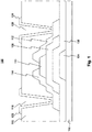
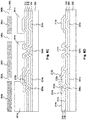
- FIG. 2 depicts an exemplary TFT device 200.
- the TFT device 200 may be employed in a liquid crystal display, an organic light-emitting-diode (OLED) device, or other electronic devices.
- TFT device 200 includes a light-emitting region 201a, a TFT device region 201b, an interconnection region 201c, and a storage capacitor region 201d formed on a substrate 202.
- the substrate 202 may be made of glass, silicon, stainless steel, or polymer, or any combination of the above materials.
- the polymer substrate may be made of polyimide (PI), polyethylene naphthalate (PEN), polyethylene terephthalate (PET), polystyrene (PS), polyethersulfone (PES), polyethylene (PE), polyvinyl chloride (PVC), etc.
- PI polyimide
- PEN polyethylene naphthalate
- PET polyethylene terephthalate
- PS polystyrene
- PS polyethersulfone
- PE polyethylene
- PVC polyvinyl chloride
- the TFT device 200 includes a first conductive layer 204 formed on the substrate 202, a first dielectric layer 206, a semiconductor layer 208, a second dielectric layer 210, and a second conductive layer 212.
- a buffer or barrier layer is formed on the substrate 202 before depositing first conductive layer 204 on the substrate 202.
- the first conductive layer 204 includes a gate electrode 204a for the TFT device region 201b, a connection pad 204b for interconnection region 201c, and a first electrode 204c for the capacitor region 201d.
- the first conductive layer 204 may be a metal (Al, Cu, Mo, Ti, Ni, W, Au, Pd, Pt, Cr, Nd, Zn, Co, Mn, or Ag), a conducting metal oxide (an oxide of zinc (Zn), indium (In), tin (Sn), gallium (Ga), hafnium (Hf), aluminum (Al), arsenic (As), cadmium (Cd), mercury (Hg), thallium (TI), lead (Pb), silver (Ag), gold (Au), germanium (Ge), antimony (Sb), bismuth (Bi), hafnium (Hf), or zirconium (Zr), etc., such as ITO, IZO, AZO, GZO, In.
- the first dielectric layer 206 covers the gate electrode 204a and the first electrode 204c, but does not completely cover the connection pad 204b so as to expose at least a portion of the connection pad 204b from the first the dielectric layer 206.
- the first the dielectric layer 206 may be made of SiO.sub.x, SiN.sub.x, SiO.sub.xN.sub.y, AlO.sub.x, Y.sub.2O.sub.3, HfO.sub.x, ZrO.sub.x, AlN, AlNO, TiO.sub.x, BaTiO.sub.3, PbTiO.sub.3, polymer, spin-on-glass (SOG), spin-on-dielectric (SOD), etc. or the mixture or multilayers or combination of the above materials.
- the semiconductor layer 208 is formed on the dielectric layer 206 and is disposed to overlap the gate electrode 204a.
- the semiconductor layer 208 may be an island and have a width greater than that of the gate electrode 204a.
- the semiconductor layer 208 may be made of amorphous silicon (a-Si), polysilicon, or metal oxide, such as oxides of zinc (Zn), indium (In), tin (Sn), gallium (Ga), hafnium (Hf), aluminum (Al), arsenic (As), cadmium (Cd), mercury (Hg), thallium (TI), lead (Pb), silver (Ag), gold (Au), germanium (Ge), antimony (Sb), bismuth (Bi), hafnium (Hf), or zirconium (Zr), etc. or combination of the above elements.
- a-Si amorphous silicon
- polysilicon or metal oxide, such as oxides of zinc (Zn), indium (In), tin (S
- the second dielectric layer 210 is disposed on the semiconductor layer 208 and the first the dielectric layer 206.
- the second dielectric layer 210 includes a dielectric island 210a that overlaps a portion of the semiconductor layer 208.
- the second dielectric layer 210 has openings to expose the connection pad 204b and first and second portions of the semiconductor layer 208 on two sides of the dielectric island 210a.
- a portion of the second dielectric layer 210 is further disposed to cover the first electrode 204c.
- one of the first the dielectric layer 206 or the second dielectric layer 210 on the first electrode 204c may be omitted.
- the second dielectric layer 210 may be made of SiO.sub.x, SiN.sub.x, SiO.sub.xN.sub.y, AlO.sub.x, Y.sub.2O.sub.3, HfO.sub.x, ZrO.sub.x, AlN, AlNO, TiO.sub.x, BaTiO.sub.3, PbTiO.sub.3, polymer, SOG, SOD, etc. or the mixture or multilayers or combination of the above materials.
- the second conductive layer 212 is disposed on the substrate 202.
- the second conductive layer 212 includes a pixel electrode portion 212a on the second dielectric layer 210, a source electrode portion 212b disposed on and covering one exposed surface of the semiconductor layer 208 to form the source electrode contact, a drain electrode portion 212c disposed on and covering another exposed surface of the semiconductor layer 208 to form the drain electrode contact, an the interconnection portion 212d disposed on the connection pad 204b, and a second electrode 212e disposed in the capacitor region 201d.
- the pixel electrode portion 212a extends to the source electrode portion 212b.
- the interconnection portion 212d extends to the drain electrode portion 212c.
- Second electrode 212e, the first electrode 204c, and first and second dielectric layers form a capacitor.
- the second conductive layer 212 can be a metal layer having a material selected from Al, Cu, Mo, Ti, Ni, W, Au, Pd, Pt, Cr, Nd, Zn, Co, Mn, Ag, etc., or the mixture or multilayer or combination of the above materials.
- the second conductive layer 212 can be a transparent conductor having a metal oxide material selected from oxides of In, Zn, Sn, Ga, Al, As, Cd, Hg, Tl, Pb, Ag, Au, Ge, Sb, Bi, Hf, Zr, etc., such as ITO, IZO, AZO, GZO, In.sub.20.sub.3, ZnO, etc., or the mixture or multilayer or combination of the above materials.
- the second conductive layer 212 may include a mixture of metal and metal oxide.
- the second conductive layer 212 can include one metal material (e.g., Zn) and one metal oxide material (e.g., ZnO) selected from the above materials.
- a TFT device may include a third conductive layer 214 disposed on the second conductive layer 212.
- a third conductive layer 214 disposed on the second conductive layer 212.
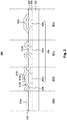
- FIG. 3 an exemplary TFT device 300 is shown FIG. 3 .
- the third conductive layer 214 is disposed to cover the second conductive layer 212 so that they are in alignment with each other.
- This the third conductive layer 214 could be selected from a material to achieve a better surface smoothness and better work function match with a top layer, such as an OLED layer in pixel electrode region.
- the third conductive layer 214 may contain a material different from the second conductive layer 212.
- the second conductive layer 212 and the third conductive layer 214 includes reflective materials (e.g., metal) and transparent conductors (e.g., metal oxide), respectively.
- the second conductive layer 212 can be made of a metal material selected from Al, Cu, Mo, Ti, Ni, W, Au, Pd, Pt, Cr, Nd, Zn, Co, Mn, Ag, etc., or the mixture or multilayer or combination of the above materials.
- the third conductive layer 214 is made of a metal oxide material selected from oxides of In, Zn, Sn, Ga, Al, As, Cd, Hg, Tl, Pb, Ag, Au, Ge, Sb, Bi, Hf, Zr, etc., such as ITO, IZO, AZO, GZO, In.sub.20.sub.3, ZnO, etc., or the mixture or multilayer or combination of the above materials. Metal oxide material has better surface smoothness and matching work function with OLED layers. Other structures and materials shown in FIG. 3 are similar to those described in connection with FIG. 2 , and thus the corresponding descriptions are omitted.
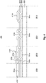
- the third conductive layer 214 may be disposed on a portion of the second conductive layer 212, but is not completely aligned with the second conductive layer 212.
- An example of such TFT device 400 is shown in FIG. 4 .
- the third conductive layer 214 is disposed on and aligned with the pixel electrode portion 212a and the source electrode portion 212b of the second conductive layer 212, but is not disposed on the drain electrode portion 212c, the interconnection portion 212d, and the second electrode portion 212e.
- the structure of the third conductive layer 214 is not limited to the configuration of FIG. 4 .
- the third conductive layer 214 may be disposed on and aligned with the pixel electrode portion 212a of the second conductive layer 212, but is not disposed on other portions of the second conductive layer 212.
- Other structures and materials shown in FIG. 4 are similar to those described in connection with FIG. 2 , and thus the corresponding descriptions are omitted.
- a substrate 202 is provided.
- the substrate 202 may be made of glass, silicon, stainless steel, or polymer.
- the polymer substrate may be made of polyimide (PI), polyethylene naphthalate (PEN), polyethylene terephthalate (PET), polystyrene (PS), polyethersulfone (PES), polyethylene (PE), polyvinyl chloride (PVC), etc.
- a first conductive layer 204 is then formed on the substrate 202, as shown in FIG. 5B .
- the first conductive layer 204 may include a metal (Al, Cu, Mo, Ti, Ni, W, Au, Pd, Pt, Cr, Nd, Zn, Co, Mn, or Ag), a conducting metal oxide (a metal oxide material selected from oxides of In, Zn, Sn, Ga, Al, As, Cd, Hg, Tl, Pb, Ag, Au, Ge, Sb, Bi, Hf, Zr, etc., such as ITO, IZO, AZO, GZO, In.sub.20.sub.3, or ZnO), or the mixture or multilayers or any combination of the above materials.
- a metal Al, Cu, Mo, Ti, Ni, W, Au, Pd, Pt, Cr, Nd, Zn, Co, Mn, or Ag
- a conducting metal oxide a metal oxide material selected from oxides of In, Zn, Sn, Ga, Al, As, Cd, Hg, Tl, Pb, Ag, Au, Ge, Sb, Bi, Hf,
- the first conductive layer 204 may be formed by various deposition techniques, such as chemical vapor deposition (CVD), plasma-enhanced CVD (PECVD), atomic layer deposition (ALD), sputtering, evaporation, or solution coating and curing.
- CVD chemical vapor deposition
- PECVD plasma-enhanced CVD
- ALD atomic layer deposition
- sputtering evaporation
- solution coating and curing evaporation
- the first conductive layer 204 is then patterned with a first mask 252 to form a gate electrode 204a, a connection pad 204b, and a first electrode 204c using a photolithographic process.
- a photolithographic process in this disclosure which includes the steps of coating a photoresist on a layer, exposing the photoresist, developing the photoresist, and etching the layer with the patterned photoresist, is disclosed in FIGS. 5G, 5H , 5I , and related text will be omitted here.
- the first mask 252 may include patterns 252a, 252b, and 252c for the photolithographic process.
- a first the dielectric layer 206 is subsequently formed on the substrate 202 and the gate electrode 204a, the connection pad 204b, and the first electrode 204c of the first conductive layer 204 as shown in FIG. 5D .
- the first the dielectric layer 206 may be formed on the substrate 202 by various deposition techniques, such as CVD, PECVD, ALD, sputtering, evaporation, or solution coating and curing.
- the material of the first the dielectric layer 206 may include SiO.sub.x, SiN.sub.x, SiO.sub.xN.sub.y, AlO.sub.x, Y.sub.2O.sub.3, HfO.sub.x, ZrO.sub.x, AlN, AlNO, TiO.sub.x, BaTiO.sub.3, PbTiO.sub.3, polymer, SOG, SOD etc. or the mixture or multilayers or combination of the above materials.
- a semiconductor layer 208 is formed on the first the dielectric layer 206 by various deposition techniques as discussed above.
- the semiconductor layer 208 may be made of amorphous silicon (a-Si), polysilicon, or a metal oxide, such as an oxide of In, Zn, Sn, Ga, Al, As, Cd, Hg, Tl, Pb, Ag, Au, Ge, Sb, Bi, Hf, Zr, etc.
- the semiconductor layer 208 is then pattern with a second mask 254 to form a semiconductor island 208a using a photolithographic process as shown in FIG. 5F .
- the second mask 254 may include patterns (e.g., 254a) for the photolithographic process.
- a second dielectric layer 210 is then formed to cover the semiconductor island 208a and the first the dielectric layer 206.
- the second dielectric layer 210 may be formed by various deposition techniques, such as CVD, PECVD, ALD, sputtering, evaporation, or solution coating and curing.
- the material of the second dielectric layer 210 may include SiO.sub.x, SiN.sub.x, SiO.sub.xN.sub.y, AlO.sub.x, Y.sub.2O.sub.3, HfO.sub.x, ZrO.sub.x, AlN, AlNO, TiO.sub.x, BaTiO.sub.3, PbTiO.sub.3, polymer, SOG, SOD, etc. or the mixture or multilayers or combination of the above materials.
- a photoresist 255 is formed on the second dielectric layer 210 to facilitate patterning second dialectic layer 210. Referring to FIG.
- the second dielectric layer 210 is then patterned through the photoresist 255 with a third mask 256.
- the photoresist 255 is exposed with light through the third mask 256 and developed to form openings 255a-255c.
- openings 255a-255c are formed in the photoresist 255 at predetermined locations using the third mask 256.
- openings 255a-255c may be formed on top of the semiconductor island 208a and the connection pad 204b as shown in FIG. 5H .
- the second dielectric layer 210 is then patterned through the photoresist 255 having openings 255a-255c. For example, referring to FIG.
- the second dielectric layer 210 is patterned by an etching process to remove materials of the second dielectric layer 210 at the openings 255a-255c so as to form a dielectric island 210a over the semiconductor island 208a and to expose first and second portions of the semiconductor island 208a to form source/drain electrode contact.
- the exposed portions of the semiconductor island 208a can be source and drain regions for a TFT.
- the etching process also exposes a portion of the connection pad 204b by removing a portion of the second dielectric layer 210 and the first the dielectric layer 206 to make an opening 260 on the connection pad 204b.
- the etching process can be a wet or dry etching, or a combination of both.
- the etchant of second dielectric layer may be selected to have good etching selectivity on the semiconductor layer to further etch the first the dielectric layer 206 without damaging the semiconductor layer.
- the etching process can continue to remove a portion of the first the dielectric layer 206 on connection pad 204a while portions of the semiconductor island 208a are exposed to the etching solutions or etching gases.
- metal oxide has good selectivity (resistance) against etching gases CH.sub.xF.sub.y/O.sub.2, and can be the material of the semiconductor island 208a when SiO.sub.x is employed for the material of first and second dielectric layers 206, 210.
- a second conductive layer 212 is formed on the substrate 202 to cover the second dielectric layer 210 and the exposed portions of the semiconductor island 208a and exposed portion of the connection pad 204b.
- the second conductive layer 212 may include a metal (Al, Cu, Mo, Ti, Ni, W, Au, Pd, Pt, Cr, Nd, Zn, Co, Mn, or Ag), a conducting metal oxide (an oxide of In, Zn, Sn, Ga, Al, As, Cd, Hg, Tl, Pb, Ag, Au, Ge, Sb, Bi, Hf, Zr, etc., such as ITO, IZO, AZO, GZO, In.sub.20.sub.3, or ZnO), or any combination of the above materials.
- a metal Al, Cu, Mo, Ti, Ni, W, Au, Pd, Pt, Cr, Nd, Zn, Co, Mn, or Ag
- a conducting metal oxide an oxide of In, Zn, Sn, Ga, Al,
- the second conductive layer 212 may be formed by various deposition techniques, such as CVD, PECVD, ALD, sputtering, evaporation, or solution coating and curing.
- the materials for the second conductive layer 212 may be transparent.
- Exemplary transparent conductive materials may include a conductive metal oxide of In, Zn, Sn, Ga, Al, As, Cd, Hg, Tl, Pb, Ag, Au, Ge, Sb, Bi, Hf, Zr, such as ITO, IZO, AZO, GZO, In.sub.20.sub.3, or ZnO, or any combination of those materials.
- the materials for the second conductive layer 212 may be reflective.
- Exemplary reflective conductive materials may include metals, e.g., Al, Cu, Mo, Ti, Ni, W, Au, Pd, Pt, Cr, Nd, Zn, Co, Mn, or Ag, or any combination of those materials.
- the second conductive layer 212 is then patterned with a fourth mask 258 to form a pixel electrode portion 212a on the second dielectric layer 210, a source electrode portion 212b disposed on and covering one exposed portion of the semiconductor island 208a, a drain electrode portion 212c disposed on and covering another exposed portion of the semiconductor island 208a, an the interconnection portion 212d disposed on the connection pad 204b, and a second electrode 212e opposed to the first electrode 204c.
- the pixel electrode portion 212a extends to and connects the source electrode portion 212b.
- the interconnection portion 212d extends to and connects the drain electrode portion 212c.
- the arrangements of these portions are not limited to these configurations.
- the interconnection portion 212d and the drain electrode portion 212c may be separated from each other or coupled to each other through another wiring pattern (not shown).
- the TFT device 200 may be formed with four masks so that the manufacturing cost may be reduced. Further, the dielectric island 210a and opening 260 leading to the connection pad 204b ( FIG. 5I ) may be formed in the same etching step to reduce processing time and increase throughput. As described above in connection with FIG. 5K , the same conductive layer 212 may be employed for a pixel electrode, source and drain electrodes, interconnection, and an electrode for a capacitor, which may further reduce the processing steps. Also, as compared to the device shown in FIG. 1 , the passivation layer 116 of FIG. 1 may be omitted to further reduce cost.
- a third conductive layer 214 may be formed on the second conductive layer 212.
- An example is depicted in FIG. 6A .
- the third conductive layer 214 may be formed on the second conductive layer 212 by various deposition techniques, such as CVD, PECVD, ALD, sputtering, evaporation, or solution coating and curing.
- the third conductive layer 214 may include a metal (Al, Cu, Mo, Ti, Ni, W, Au, Pd, Pt, Cr, Nd, Zn, Co, Mn, or Ag), a conducting metal oxide (an oxide of In, Zn, Sn, Ga, Al, As, Cd, Hg, Ti, Pb, Ag, Au, Ge, Sb, Bi, Hf, Zr, etc., such as ITO, IZO, AZO, GZO, In.sub.20.sub.3, or ZnO), or any mixture or combination of the above materials.
- a metal Al, Cu, Mo, Ti, Ni, W, Au, Pd, Pt, Cr, Nd, Zn, Co, Mn, or Ag
- a conducting metal oxide an oxide of In, Zn, Sn, Ga, Al, As, Cd, Hg, Ti, Pb, Ag, Au, Ge, Sb, Bi, Hf, Zr, etc., such as ITO, IZO, AZO, G
- the third conductive layer 214 includes a material different from that of the second conductive layer 212.
- the third conductive layer 214 may include a metal material different from a metal material of the second conductive layer 212; the third conductive layer 214 may include a metal oxide while the second conductive layer 212 may include a metal; the third conductive layer 214 may include a mixture of metal oxide and metal while the second conductive layer 212 may include a metal.
- the third conductive layer 214 may consist of a metal material different from a metal material of the second conductive layer 212; the third conductive layer 214 may consist of a metal oxide while the second conductive layer 212 may consist of a metal; the third conductive layer 214 may consist of a metal oxide (or oxides) and a metal (metals) while the second conductive layer 212 may consist of a metal (metals).
- the third conductive layer 214 may be transparent (e.g., a metal oxide) and the second conductive layer 212 may be reflective (e.g., a metal), or vice versa.
- the materials of the third conductive layer 214 may be selected to match a display medium layer (e.g., OLED layers) disposed on top in pixel electrode regions for a better carrier injection.
- a display medium layer e.g., OLED layers
- the second conductive layer 212 and the third conductive layer 214 are then patterned with the fourth mask 258 to form a pixel electrode portion 212a, 214a, a source electrode portion 212b, 214b, a drain electrode portion 212c, 214c, an the interconnection portion 212d, 214d, and a second electrode 212e, 214e.
- the pixel electrode portion 212a, 214a is arranged to extend to and connect the source electrode portion 212b, 214b.
- the interconnection portion 212d, 214d is arranged to extend to and connect the drain electrode portion 212c, 214c.
- the arrangements of these portions are not limited to these configurations.
- the interconnection portion 212d, 214d and the drain electrode portion 212c, 214c may be separated from each other or coupled to each other through another wiring pattern (not shown).
- the third conductive layer 214 is patterned so that all of its patterns are substantially aligned with the patterns of the second conductive layer 212, in a one-to-one manner.
- the edges of the patterns of the second conductive layer 212 and the third conductive layer 214 may be offset from each other. Accordingly, a TFT device having three conductive layers may be formed with four masks.
- the second conductive layer 212 and the third conductive layer 214 may be patterned with a gray-tone or half-tone mask.
- An exemplary half-tone mask is shown in FIG. 6C .
- mask 260 includes three areas: area 260a having the lowest light transmission rate, area 260b having the highest light transmission rate, and area 260c having light transmission rate between those of areas 260a and 206b.
- a photoresist is coated on the third conductive layer 214 similar to photoresist depicted in FIG. 5G . The photoresist is then exposed with light through mask 260 and subjected to a developing process. Referring to FIG.
- photoresist layers 261a, 261b, and 261c are formed. Specifically, photoresist layer 261a under mask area 260a has the greatest thickness as it receives less light exposure. Photoresist layer under mask area 260b is removed from the surface of the third conductive layer 214 in the developing process as it is thoroughly exposed with light. Photoresist layer 261c under mask area 260c has a thickness less than the thickness of photoresist layer 261a for it receives light exposure less than photoresist layer 261a does.
- the second conductive layer 212 and the third conductive layer 214 with photoresist layers 261a and 261c are then etched. Referring to FIG. 6D , after etching step, regions under photoresist layer 261a are protected so that both the second conductive layer 212 and the third conductive layer 214 remain, forming the pixel electrode portion 212a, 214a, and the source electrode portion 212b, 214b. Regions under photoresist layer 261c are partially protected so that only the second conductive layer 212 remains, forming the drain electrode portion 212c, the interconnection portion 212d, and the second electrode portion 212e.
- Regions of the second conductive layer 212 and the third conductive layer 214 not covered with a photoresist layer are etched to form an opening separating the source electrode portion 212b, 214b and the drain electrode portion 212c, and an opening separating the interconnection portion 212d and the second electrode portion 212e.
- the selection of materials for the second conductive layer 212 and the third conductive layer 214 in FIGS. 6C and 6D are similar to those in FIGS. 6A and 6B and thus is omitted here. Accordingly, a TFT device having three conductive layers may be formed with four masks.
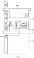
- FIGS. 7A-7D depict exemplary pixel layouts of this disclosure.
- a first conductive layer is deposited on a substrate, similar to those depicted in FIG. 5B .
- FIG. 7A shows exemplary patterns of the first conductive layer after being patterned with a first mask.
- the patterns of the first conductive layer include a first row/gate line 702a, a pad region 702b, a second row/gate line 702c, and a gate electrode region 702d coupled to second row line 702c.
- a first dielectric layer and a semiconductor layer are subsequently deposited on the substrate to cover the patterns of the first conductive layer, similar to those depicted in FIG. 5E .
- FIG. 7B depicts exemplary patterns of a semiconductor layer after being patterned with a second mask.
- the patterns of the semiconductor layer include a first semiconductor island 704a and a second semiconductor island 704b.
- FIG. 7C depicts exemplary patterns of the first and second dielectric layers after being patterned with a third mask.
- the patterns of the dielectric layers include first and second openings 706a, 706b in the second dielectric layer to reach first semiconductor island 704a; third and fourth openings in both the first and second dielectric layers to reach pad region 702b and first row line 702a, respectively; and fifth and sixth openings 706e, 706f in the second dielectric layer to reach second semiconductor island 704b.
- openings 706a and 706b expose surfaces of first semiconductor island 704a; opening 706c exposes a surface of pad region 702b; opening 706d exposes a surface of first row line 702a; openings 706e and 706f expose surfaces of second semiconductor island 704b.
- FIG. 7D depicts exemplary patterns of the second conductive after being patterned with a fourth mask.
- the patterns of the second conductive layer include a column/data line 708a, pad regions 708b, 708c, 708d, and a pixel electrode portion 708e.
- the column line 708a covers first opening 706a and connects to the first semiconductor island 704a.
- the pad region 708b covers the second opening 706b and third opening 706c, and connects to the first semiconductor island 704a and pad region 702b of the first conductive layer.
- the pad region 708b overlaps a portion of the first row line 702a so as to form a capacitor.
- the pad region 708c covers the fourth opening 706d and fifth opening 706e and connects to the first row line 702a and second semiconductor island 704b.
- the pad region 708d covers the sixth opening 706f and extends to the pixel electrode portion 708e. Accordingly, a TFT device having two conductive layers may be formed with four masks.
- the column line 708a, pad regions 708b, 708c, 708d, and pixel electrode portion 708e may contain two conductive layers having different materials, similar to those depicted in FIG. 6B . As such, a TFT device having three conductive layers may also be formed with four masks.
- some of the column line 708a, pad regions 708b, 708c, 708d, and pixel electrode portion 708e may contain two conductive layers while others contain one conductive layer, similar to those depicted in FIG. 6D .
- the pad region 708d and pixel electrode portion 708e contain two different conductive layers while the column line 708a and pad regions 708b, 708c contain a single conductive layer.
- such configuration may also be formed using four masks including a half-tone mask.
- the first conductive layer may form part of both row and column lines.
- Exemplary pixel layouts are depicted in FIGS. 8A-8D .
- a first conductive layer is deposited on a substrate, similar to those depicted in FIG. 5B .
- FIG. 8A shows exemplary patterns of the first conductive layer after being patterned with a first mask.
- the patterns of the first conductive layer include a first row line 802a, a pad region 802b, a second row line 802c, a gate electrode region 802d, and a plurality of line segments (connection pads) 802e extending in the column direction. Line segments 802e do not intersect row lines 802a and 802c.
- FIG. 8B depicts exemplary patterns of a semiconductor layer after being patterned with a second mask.
- the patterns of the semiconductor layer include a first semiconductor island 804a and a second semiconductor island 804b.
- FIG. 8C depicts exemplary patterns of the first and second dielectric layers after being patterned with a third mask.
- the patterns of the dielectric layers include first openings 806a in the second dielectric layer to reach semiconductor islands 804a, 804b, and second openings 806b in both the first and second dielectric layers to reach the first conductive layer.
- the first openings 806a expose surfaces of the first semiconductor island 804a and second semiconductor island 804b
- the second openings 806b expose surfaces of a first row line 802a, a pad region 802b, and line segments 802e.
- at least one opening 806b is arranged on each of line segments 802e.
- FIG. 8D depicts exemplary patterns of the second conductive after being patterned with a fourth mask.
- the patterns of the second conductive layer include a column line 808a, pad regions 808b, 808c, 808d, and a pixel electrode portion 808e.
- the column line 808a covers the second openings 806b on the line segments 802e and first opening 806a so as to connect to the first semiconductor island 804a.
- the pad region 808b covers a first opening 806a and a second opening 806b over on the pad region 802b so as to connect the first semiconductor island 804a and pad region 802b of the first conductive layer.
- the pad region 808b overlaps a portion of the first row line 802a so as to form a capacitor.
- the pad region 808c covers a first opening 808a on the second semiconductor island 804b and covers a second opening 806b on the first row line 802a so as to connect the first row line 802a and second semiconductor island 804b.
- the pad region 808d covers a first opening 806a on the second semiconductor island 804b and extends to the pixel electrode portion 808e.
- lines run in the column direction include two conductive layers and thus may have a lower resistance to reduce single delay in the column lines.
- a TFT device having such configuration may also be formed with four masks.
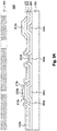
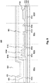
- FIG. 9 shows an AMOLED device having a TFT device.
- AMOLED device 900 includes a light-emitting region 901a, a TFT device region 901b, an interconnection region 901c, and a thin film capacitor region 901d, formed on a substrate 902.
- the substrate 902 may be made of glass, silicon, stainless steel, or polymer.
- the polymer substrate may be made of polyimide (PI), polyethylene naphthalate (PEN), polyethylene terephthalate (PET), polystyrene (PS), polyethersulfone (PES), polyethylene (PE), polyvinyl chloride (PVC), etc.
- PI polyimide
- PEN polyethylene naphthalate
- PET polyethylene terephthalate
- PS polystyrene
- PS polyethersulfone
- PE polyethylene
- PVC polyvinyl chloride
- AMOLED device 900 includes a first conductive layer 904 formed on substrate 902, a first dielectric layer 906, a semiconductor layer 908a, a second dielectric layer 910, and a second conductive layer 912.
- a buffer layer is formed on substrate 902 before depositing the first conductive layer on substrate 902.
- First conductive layer 904 includes a gate electrode 904a of TFT device region 901b, a connection pad 904b for interconnection region 901c, and a first electrode 904c for capacitor region 901d.
- the first conductive layer 904 may be a metal (Al, Cu, Mo, Ti, Ni, W, Au, Pd, Pt, Cr, Nd, Zn, Co, Mn, or Ag), a conducting metal oxide (an oxide of In, Zn, Sn, Ga, Al, As, Cd, Hg, Tl, Pb, Ag, Au, Ge, Sb, Bi, Hf, Zr, etc., such as ITO, IZO, AZO, GZO, In.sub.20.sub.3, or ZnO), or the mixture or multilayers or any combination of the above materials.
- the first dielectric layer 906 covers the gate electrode 904a and first electrode 904c, but does not completely cover the connection pad 904b so as to expose at least a portion of connection pad 904b from the first dielectric layer 906.
- the first dialectic layer 906 may be made of SiO.sub.x, SiN.sub.x, SiO.sub.xN.sub.y, AlO.sub.x, Y.sub.2O.sub.3, HfO.sub.x, ZrO.sub.x, AlN, AlNO, TiO.sub.x, BaTiO.sub.3, PbTiO.sub.3, polymer, SOG, SOD, etc. or the mixture or multilayers or combination of the above materials.
- the semiconductor layer 908a is formed on the dielectric layer 906 and is disposed to overlap the gate electrode 904a. In some embodiments, the semiconductor layer 908a may have a width greater than that of the gate electrode 901a.
- the semiconductor layer 908a may be made of amorphous silicon (a-Si) or a metal oxide, such as an oxide of In, Zn, Sn, Ga, Al, As, Cd, Hg, Tl, Pb, Ag, Au, Ge, Sb, Bi, Hf, Zr, etc.
- the second dielectric layer 910 is disposed on the semiconductor layer 908a and first dielectric layer 906.
- the second dielectric layer 910 includes a dielectric island 910a that overlaps a portion of the semiconductor layer 908a.
- the second dielectric layer 910 has openings to expose the connection pad 904b and first and second portions of the semiconductor layer 908a on two sides of the dielectric island 910a. Referring to FIG. 9 , a portion of the second dielectric layer 910 is disposed to cover the first electrode 904c. In some embodiments, one of the first dielectric layer 906 or the second dielectric layer 910 on the first electrode 904c may be omitted.
- the second dialectic layer 910 may be made of SiO.sub.x, SiN.sub.x, SiO.sub.xN.sub.y, AlO.sub.x, Y.sub.2O.sub.3, HfO.sub.x, ZrO.sub.x, AlN, AlNO, TiO.sub.x, BaTiO.sub.3, PbTiO.sub.3, polymer, SOG, SOD, etc. or the mixture or multilayers or combination of the above materials.
- the second conductive layer 912 is disposed on the substrate 902.
- the second conductive layer 912 includes a pixel electrode portion 912a on the dielectric layer, a source electrode portion 912b disposed on and covering one portion of the exposed semiconductor layer, a drain electrode portion 912c disposed on and covering another portion of the exposed semiconductor layer, an interconnection portion 912d disposed on the connection pad 204b, and a second electrode 912e disposed in capacitor region 901d.
- pixel electrode portion 912a extends to source electrode portion 912b.
- the interconnection portion 912d extends to the drain electrode portion 912c.
- the second electrode 912e, first electrode 904c, and first and second dielectric layers forms a capacitor.
- the second conductive layer 912 can be a metal layer having a material selected from Al, Cu, Mo, Ti, Ni, W, Au, Pd, Pt, Cr, Nd, Zn, Co, Mn, Ag, etc., or the mixture or multilayer or combination of the above materials.
- the second conductive layer 912 can be a transparent conductor having a metal oxide material selected from an oxide of In, Zn, Sn, Ga, Al, As, Cd, Hg, TI, Pb, Ag, Au, Ge, Sb, Bi, Hf, Zr, etc., such as ITO, IZO, AZO, GZO, In.sub.20.sub.3, ZnO, etc., or the mixture or multilayer or combination of the above materials.
- the second conductive layer 912 may include a mixture of metal and metal oxide.
- the second conductive layer 212 can include one metal material (e.g., Zn) and one metal oxide material (e.g., ZnO) selected from the above materials.
- AMOLED device 900 further includes a pixel defining layer 918, an OLED layer 920, an OLED cathode layer 922, and an encapsulation 924.
- the pixel defining layer 918 is disposed in regions other than where the pixel electrode 912a is located.
- the OLED layer 920 is disposed on the pixel electrode 912a and on the pixel defining layer 918.
- the pixel electrode 912a and OLED cathode layer 922 sandwich OLED layer 920 to provide currents to the OLED layer 920.
- the encapsulation 924 is disposed on the OLED cathode layer 922 to protect the underlying layers.
Landscapes
- Engineering & Computer Science (AREA)
- Microelectronics & Electronic Packaging (AREA)
- Manufacturing & Machinery (AREA)
- Thin Film Transistor (AREA)
- Internal Circuitry In Semiconductor Integrated Circuit Devices (AREA)
- Devices For Indicating Variable Information By Combining Individual Elements (AREA)
Abstract
Description
- This application claims priority to provisional application No.
62/041,129 14/593, 812 - The present disclosure relates to a transistor, and particularly to a thin-film transistor and its application in a display, and a method for manufacturing the same.
- Flat panel displays have been in the market in the applications such as, TVs, monitors, cell phones, small phones, personal digital assistants (PDAs), etc. Particularly, due to its capability of being in large size and high definition, active matrix flat panel displays are widely integrated in large-sized TVs and high-definition hand-held devices.
- An active matrix flat panel display generally includes an array of thin-film transistors (TFT) to control a light emission device. An
exemplary TFT device 100 is shown inFIG. 1 . Referring toFIG. 1 , theTFT device 100 includes asubstrate 102, agate electrode 104 disposed on thesubstrate 102, adielectric layer 106 disposed on thesubstrate 102 and thegate electrode 104, asemiconductor layer 108 disposed on thedielectric layer 106, anetching stop 110 disposed on thesemiconductor layer 108, adrain electrode 112 disposed on one side of and in contact with thesemiconductor layer 108, asource electrode 114 disposed on another side of and in contact with thesemiconductor layer 108, apassivation layer 116 disposed on top of the above layers, afirst contact hole 118 formed in thepassivation layer 116 to reach thesource electrode 114, asecond contact hole 120 formed in thepassivation layer 116 to reach thedrain electrode 112, thepixel electrode 122 disposed in thefirst contact hole 118, and adata electrode 124 disposed in thesecond contact hole 120. - To form the TFT device as shown in
FIG. 1 , at least six masks are employed to form the pattern of the device layers. Specifically, one mask is needed for each of thegate electrode 104,semiconductor layer 108,etch stop 110,source electrode 114 anddrain electrode 112,contact holes pixel electrode 122. -
Etch stop 110 is employed to protect thesemiconductor layer 108 from being damaged by etchants during the patterning and etching steps to form source anddrain electrodes pattern etch stop 110 itself, which increases the fabrication cost and decreases the processing throughput. Further, thepassivation layer 116 is employed to protect theunderlying device layers 104∼114 from being affected by the environment. - Therefore, there is a need to reduce the number of the masks employed to fabricate a TFT device to increase manufacturing throughput and decrease the cost.
- Consistent with this disclosure, a thin film transistor (TFT) device is provided. The TFT device includes a first conductive layer including a gate electrode, and a connection pad. The TFT device further includes a first dielectric layer covering the gate electrode. The connection pad is exposed from the first dielectric layer. The TFT device further includes a semiconductor layer disposed on the dielectric layer and overlapping the gate electrode. The TFT device further includes a second dielectric layer disposed on the semiconductor layer and the first dielectric layer so as to expose first and second portions of the semiconductor layer and the connection pad. The TFT device further includes a second conductive layer which includes a source electrode portion covering the first portion of the semiconductor layer; a pixel electrode portion extending to the source electrode portion; a drain electrode portion covering the second portion of the semiconductor layer; and an interconnection portion disposed on the connection pad and extending to the drain electrode portion.
- Consistent with this disclosure, a method for forming a thin film transistor device is provided. The method includes depositing a first conductive layer on a substrate; patterning the first conductive layer with a first mask to form a gate electrode, and a connection pad; depositing a first dielectric layer over the substrate to cover the gate electrode, and the connection pad; depositing a semiconductor layer on the first dielectric layer; patterning the semiconductor layer with a second mask to form a semiconductor island to overlap the gate electrode; and depositing a second dielectric layer on the substrate; patterning the second dielectric layer with a third mask to expose first and second portions of the semiconductor island and forming a dielectric island on the semiconductor island, and patterning the second dielectric layer and the first dielectric layer with the third mask to expose the connection pad; depositing a second conductive layer on the substrate so that the second conductive layer is in contact with the connection pad; and patterning second conductive layer with a fourth mask.
- Additional aspects and advantages of embodiments of present invention will be given in part in the following descriptions, become apparent in part from the following descriptions, or be learned from the practice of the embodiments of the present invention.
- These and other aspects and advantages of embodiments of the present invention will become apparent and more readily appreciated from the following descriptions made with reference to the accompanying drawings, in which:
-
FIG. 1 shows a conventional TFT device; -
FIG. 2 shows a TFT device consistent with some embodiments of this disclosure; -
FIG. 3 shows another TFT device consistent with some embodiments of this disclosure; -
FIG. 4 shows yet another TFT device consistent with some embodiments of this disclosure; -
FIGS. 5A-5K depict exemplary methods of forming TFT devices consistent with some embodiments of this disclosure; -
FIGS. 6A-6D depict exemplary methods of forming TFT devices consistent with some embodiments of this disclosure; -
FIGS. 7A-7D depict exemplary methods of forming TFT devices consistent with some embodiments of this disclosure; -
FIGS. 8A-8D depict exemplary methods of forming TFT devices consistent with some embodiments of this disclosure; and -
FIG. 9 shows an exemplary active matrix organic light-emitting diode device consistent with some embodiments of this disclosure. - Reference will be made in detail to embodiments of the present invention. The same or similar elements and the elements having same or similar functions are denoted by like reference numerals throughout the descriptions. The embodiments described herein with reference to drawings are explanatory, illustrative, and used to generally understand the present invention. The embodiments shall not be construed to limit the present invention.
- In the description of the present disclosure, it is to be understood that terms such as "first" and "second" are used herein for purposes of description and are not intended to indicate or imply relative importance or significance or to imply the number of the technical features. Thus, the technical feature limited by "first" and "second" may indicate or imply to include one or more technical features. In the description of the present invention, "a plurality of" means two or more than two, unless otherwise specified.
- In the present invention, it is understood that, unless specified or limited otherwise, the terms "mounted," "connected," "coupled," "fixed" and the like are used broadly, and may be, for example, fixed connections, detachable connections, or integral connections; may also be mechanical connections, or may be electrical connections or intercommunication; may also be direct connections or indirect connections via intervening structures; may also be inner communications of two elements, which can be understood by those skilled in the art according to specific situations
- Various embodiments and examples are provided in the following description to implement different structures of the present disclosure. In order to simplify the present disclosure, certain elements and settings will be described. However, these elements and settings are only by way of example and are not intended to limit the present disclosure. In addition, reference numerals may be repeated in different examples in the present disclosure. This repeating is for the purpose of simplification and clarity and does not refer to relations between different embodiments and/or settings. Furthermore, examples of different processes and materials are provided in the present disclosure. However, it would be appreciated by those skilled in the art that other processes and/or materials may be also applied.
-
FIG. 2 depicts anexemplary TFT device 200. TheTFT device 200 may be employed in a liquid crystal display, an organic light-emitting-diode (OLED) device, or other electronic devices.TFT device 200 includes a light-emitting region 201a, aTFT device region 201b, aninterconnection region 201c, and astorage capacitor region 201d formed on asubstrate 202. Thesubstrate 202 may be made of glass, silicon, stainless steel, or polymer, or any combination of the above materials. The polymer substrate may be made of polyimide (PI), polyethylene naphthalate (PEN), polyethylene terephthalate (PET), polystyrene (PS), polyethersulfone (PES), polyethylene (PE), polyvinyl chloride (PVC), etc. - The
TFT device 200 includes a firstconductive layer 204 formed on thesubstrate 202, a firstdielectric layer 206, asemiconductor layer 208, a seconddielectric layer 210, and a secondconductive layer 212. In some embodiments, a buffer or barrier layer is formed on thesubstrate 202 before depositing firstconductive layer 204 on thesubstrate 202. - The first
conductive layer 204 includes agate electrode 204a for theTFT device region 201b, aconnection pad 204b forinterconnection region 201c, and afirst electrode 204c for thecapacitor region 201d. The firstconductive layer 204 may be a metal (Al, Cu, Mo, Ti, Ni, W, Au, Pd, Pt, Cr, Nd, Zn, Co, Mn, or Ag), a conducting metal oxide (an oxide of zinc (Zn), indium (In), tin (Sn), gallium (Ga), hafnium (Hf), aluminum (Al), arsenic (As), cadmium (Cd), mercury (Hg), thallium (TI), lead (Pb), silver (Ag), gold (Au), germanium (Ge), antimony (Sb), bismuth (Bi), hafnium (Hf), or zirconium (Zr), etc., such as ITO, IZO, AZO, GZO, In.sub.20.sub.3, or ZnO), or the mixture or multilayers or any combination of the above materials. - The
first dielectric layer 206 covers thegate electrode 204a and thefirst electrode 204c, but does not completely cover theconnection pad 204b so as to expose at least a portion of theconnection pad 204b from the first thedielectric layer 206. The first thedielectric layer 206 may be made of SiO.sub.x, SiN.sub.x, SiO.sub.xN.sub.y, AlO.sub.x, Y.sub.2O.sub.3, HfO.sub.x, ZrO.sub.x, AlN, AlNO, TiO.sub.x, BaTiO.sub.3, PbTiO.sub.3, polymer, spin-on-glass (SOG), spin-on-dielectric (SOD), etc. or the mixture or multilayers or combination of the above materials. - The
semiconductor layer 208 is formed on thedielectric layer 206 and is disposed to overlap thegate electrode 204a. In some embodiments, thesemiconductor layer 208 may be an island and have a width greater than that of thegate electrode 204a. Thesemiconductor layer 208 may be made of amorphous silicon (a-Si), polysilicon, or metal oxide, such as oxides of zinc (Zn), indium (In), tin (Sn), gallium (Ga), hafnium (Hf), aluminum (Al), arsenic (As), cadmium (Cd), mercury (Hg), thallium (TI), lead (Pb), silver (Ag), gold (Au), germanium (Ge), antimony (Sb), bismuth (Bi), hafnium (Hf), or zirconium (Zr), etc. or combination of the above elements. - The
second dielectric layer 210 is disposed on thesemiconductor layer 208 and the first thedielectric layer 206. Thesecond dielectric layer 210 includes adielectric island 210a that overlaps a portion of thesemiconductor layer 208. Thesecond dielectric layer 210 has openings to expose theconnection pad 204b and first and second portions of thesemiconductor layer 208 on two sides of thedielectric island 210a. Referring toFIG. 2 , a portion of thesecond dielectric layer 210 is further disposed to cover thefirst electrode 204c. In some embodiments, one of the first thedielectric layer 206 or thesecond dielectric layer 210 on thefirst electrode 204c may be omitted. Thesecond dielectric layer 210 may be made of SiO.sub.x, SiN.sub.x, SiO.sub.xN.sub.y, AlO.sub.x, Y.sub.2O.sub.3, HfO.sub.x, ZrO.sub.x, AlN, AlNO, TiO.sub.x, BaTiO.sub.3, PbTiO.sub.3, polymer, SOG, SOD, etc. or the mixture or multilayers or combination of the above materials. - Referring to
FIG. 2 , the secondconductive layer 212 is disposed on thesubstrate 202. the secondconductive layer 212 includes apixel electrode portion 212a on thesecond dielectric layer 210, asource electrode portion 212b disposed on and covering one exposed surface of thesemiconductor layer 208 to form the source electrode contact, adrain electrode portion 212c disposed on and covering another exposed surface of thesemiconductor layer 208 to form the drain electrode contact, an theinterconnection portion 212d disposed on theconnection pad 204b, and asecond electrode 212e disposed in thecapacitor region 201d. As shown inFIG. 2 , thepixel electrode portion 212a extends to thesource electrode portion 212b. Similarly, theinterconnection portion 212d extends to thedrain electrode portion 212c.Second electrode 212e, thefirst electrode 204c, and first and second dielectric layers form a capacitor. - In some embodiments, the second
conductive layer 212 can be a metal layer having a material selected from Al, Cu, Mo, Ti, Ni, W, Au, Pd, Pt, Cr, Nd, Zn, Co, Mn, Ag, etc., or the mixture or multilayer or combination of the above materials. In other embodiments, the secondconductive layer 212 can be a transparent conductor having a metal oxide material selected from oxides of In, Zn, Sn, Ga, Al, As, Cd, Hg, Tl, Pb, Ag, Au, Ge, Sb, Bi, Hf, Zr, etc., such as ITO, IZO, AZO, GZO, In.sub.20.sub.3, ZnO, etc., or the mixture or multilayer or combination of the above materials. In some embodiments, the secondconductive layer 212 may include a mixture of metal and metal oxide. For example, the secondconductive layer 212 can include one metal material (e.g., Zn) and one metal oxide material (e.g., ZnO) selected from the above materials. - Furthermore, in some embodiments, a TFT device may include a third
conductive layer 214 disposed on the secondconductive layer 212. For example, anexemplary TFT device 300 is shownFIG. 3 . Referring toFIG. 3 , the thirdconductive layer 214 is disposed to cover the secondconductive layer 212 so that they are in alignment with each other. This the thirdconductive layer 214 could be selected from a material to achieve a better surface smoothness and better work function match with a top layer, such as an OLED layer in pixel electrode region. The thirdconductive layer 214 may contain a material different from the secondconductive layer 212. In some embodiments, the secondconductive layer 212 and the thirdconductive layer 214 includes reflective materials (e.g., metal) and transparent conductors (e.g., metal oxide), respectively. For example, the secondconductive layer 212 can be made of a metal material selected from Al, Cu, Mo, Ti, Ni, W, Au, Pd, Pt, Cr, Nd, Zn, Co, Mn, Ag, etc., or the mixture or multilayer or combination of the above materials. The thirdconductive layer 214 is made of a metal oxide material selected from oxides of In, Zn, Sn, Ga, Al, As, Cd, Hg, Tl, Pb, Ag, Au, Ge, Sb, Bi, Hf, Zr, etc., such as ITO, IZO, AZO, GZO, In.sub.20.sub.3, ZnO, etc., or the mixture or multilayer or combination of the above materials. Metal oxide material has better surface smoothness and matching work function with OLED layers. Other structures and materials shown inFIG. 3 are similar to those described in connection withFIG. 2 , and thus the corresponding descriptions are omitted. - In some embodiments, the third
conductive layer 214 may be disposed on a portion of the secondconductive layer 212, but is not completely aligned with the secondconductive layer 212. An example ofsuch TFT device 400 is shown inFIG. 4 . Referring toFIG. 4 , the thirdconductive layer 214 is disposed on and aligned with thepixel electrode portion 212a and thesource electrode portion 212b of the secondconductive layer 212, but is not disposed on thedrain electrode portion 212c, theinterconnection portion 212d, and thesecond electrode portion 212e. However, the structure of the thirdconductive layer 214 is not limited to the configuration ofFIG. 4 . For example, the thirdconductive layer 214 may be disposed on and aligned with thepixel electrode portion 212a of the secondconductive layer 212, but is not disposed on other portions of the secondconductive layer 212. Other structures and materials shown inFIG. 4 are similar to those described in connection withFIG. 2 , and thus the corresponding descriptions are omitted. - Next, methods for forming TFT devices are described below. Referring to
FIG. 5A , asubstrate 202 is provided. Thesubstrate 202 may be made of glass, silicon, stainless steel, or polymer. The polymer substrate may be made of polyimide (PI), polyethylene naphthalate (PEN), polyethylene terephthalate (PET), polystyrene (PS), polyethersulfone (PES), polyethylene (PE), polyvinyl chloride (PVC), etc. A firstconductive layer 204 is then formed on thesubstrate 202, as shown inFIG. 5B . The firstconductive layer 204 may include a metal (Al, Cu, Mo, Ti, Ni, W, Au, Pd, Pt, Cr, Nd, Zn, Co, Mn, or Ag), a conducting metal oxide (a metal oxide material selected from oxides of In, Zn, Sn, Ga, Al, As, Cd, Hg, Tl, Pb, Ag, Au, Ge, Sb, Bi, Hf, Zr, etc., such as ITO, IZO, AZO, GZO, In.sub.20.sub.3, or ZnO), or the mixture or multilayers or any combination of the above materials. The firstconductive layer 204 may be formed by various deposition techniques, such as chemical vapor deposition (CVD), plasma-enhanced CVD (PECVD), atomic layer deposition (ALD), sputtering, evaporation, or solution coating and curing. - Referring to
FIG. 5C , the firstconductive layer 204 is then patterned with afirst mask 252 to form agate electrode 204a, aconnection pad 204b, and afirst electrode 204c using a photolithographic process. A detailed description of a photolithographic process in this disclosure, which includes the steps of coating a photoresist on a layer, exposing the photoresist, developing the photoresist, and etching the layer with the patterned photoresist, is disclosed inFIGS. 5G, 5H ,5I , and related text will be omitted here. Thefirst mask 252 may includepatterns dielectric layer 206 is subsequently formed on thesubstrate 202 and thegate electrode 204a, theconnection pad 204b, and thefirst electrode 204c of the firstconductive layer 204 as shown inFIG. 5D . The first thedielectric layer 206 may be formed on thesubstrate 202 by various deposition techniques, such as CVD, PECVD, ALD, sputtering, evaporation, or solution coating and curing. The material of the first thedielectric layer 206 may include SiO.sub.x, SiN.sub.x, SiO.sub.xN.sub.y, AlO.sub.x, Y.sub.2O.sub.3, HfO.sub.x, ZrO.sub.x, AlN, AlNO, TiO.sub.x, BaTiO.sub.3, PbTiO.sub.3, polymer, SOG, SOD etc. or the mixture or multilayers or combination of the above materials. - Referring to
FIG. 5E , asemiconductor layer 208 is formed on the first thedielectric layer 206 by various deposition techniques as discussed above. Thesemiconductor layer 208 may be made of amorphous silicon (a-Si), polysilicon, or a metal oxide, such as an oxide of In, Zn, Sn, Ga, Al, As, Cd, Hg, Tl, Pb, Ag, Au, Ge, Sb, Bi, Hf, Zr, etc. Thesemiconductor layer 208 is then pattern with a second mask 254 to form asemiconductor island 208a using a photolithographic process as shown inFIG. 5F . The second mask 254 may include patterns (e.g., 254a) for the photolithographic process. - Referring to
FIG. 5G , asecond dielectric layer 210 is then formed to cover thesemiconductor island 208a and the first thedielectric layer 206. Thesecond dielectric layer 210 may be formed by various deposition techniques, such as CVD, PECVD, ALD, sputtering, evaporation, or solution coating and curing. The material of thesecond dielectric layer 210 may include SiO.sub.x, SiN.sub.x, SiO.sub.xN.sub.y, AlO.sub.x, Y.sub.2O.sub.3, HfO.sub.x, ZrO.sub.x, AlN, AlNO, TiO.sub.x, BaTiO.sub.3, PbTiO.sub.3, polymer, SOG, SOD, etc. or the mixture or multilayers or combination of the above materials. Referring toFIGS. 5G and 5H , aphotoresist 255 is formed on thesecond dielectric layer 210 to facilitate patterning seconddialectic layer 210. Referring toFIG. 5H , thesecond dielectric layer 210 is then patterned through thephotoresist 255 with athird mask 256. For example, thephotoresist 255 is exposed with light through thethird mask 256 and developed to formopenings 255a-255c. Specifically,openings 255a-255c are formed in thephotoresist 255 at predetermined locations using thethird mask 256. For example,openings 255a-255c may be formed on top of thesemiconductor island 208a and theconnection pad 204b as shown inFIG. 5H . Thesecond dielectric layer 210 is then patterned through thephotoresist 255 havingopenings 255a-255c. For example, referring toFIG. 5I , thesecond dielectric layer 210 is patterned by an etching process to remove materials of thesecond dielectric layer 210 at theopenings 255a-255c so as to form adielectric island 210a over thesemiconductor island 208a and to expose first and second portions of thesemiconductor island 208a to form source/drain electrode contact. The exposed portions of thesemiconductor island 208a can be source and drain regions for a TFT. Further, the etching process also exposes a portion of theconnection pad 204b by removing a portion of thesecond dielectric layer 210 and the first thedielectric layer 206 to make anopening 260 on theconnection pad 204b. The etching process can be a wet or dry etching, or a combination of both. The etchant of second dielectric layer may be selected to have good etching selectivity on the semiconductor layer to further etch the first thedielectric layer 206 without damaging the semiconductor layer. - In some embodiments, because the materials in the
semiconductor island 208a may be resistant to etching solutions of a wet process or etching gases of a dry process, after removing a portion of thesecond dielectric layer 210, the etching process can continue to remove a portion of the first thedielectric layer 206 onconnection pad 204a while portions of thesemiconductor island 208a are exposed to the etching solutions or etching gases. For example, metal oxide has good selectivity (resistance) against etching gases CH.sub.xF.sub.y/O.sub.2, and can be the material of thesemiconductor island 208a when SiO.sub.x is employed for the material of first and seconddielectric layers - Next, referring to
FIG. 5J , a secondconductive layer 212 is formed on thesubstrate 202 to cover thesecond dielectric layer 210 and the exposed portions of thesemiconductor island 208a and exposed portion of theconnection pad 204b. The secondconductive layer 212 may include a metal (Al, Cu, Mo, Ti, Ni, W, Au, Pd, Pt, Cr, Nd, Zn, Co, Mn, or Ag), a conducting metal oxide (an oxide of In, Zn, Sn, Ga, Al, As, Cd, Hg, Tl, Pb, Ag, Au, Ge, Sb, Bi, Hf, Zr, etc., such as ITO, IZO, AZO, GZO, In.sub.20.sub.3, or ZnO), or any combination of the above materials. The secondconductive layer 212 may be formed by various deposition techniques, such as CVD, PECVD, ALD, sputtering, evaporation, or solution coating and curing. In some embodiments, for example, as applied in bottom-emission active-matrix OLED (AMOLED) devices, the materials for the secondconductive layer 212 may be transparent. Exemplary transparent conductive materials may include a conductive metal oxide of In, Zn, Sn, Ga, Al, As, Cd, Hg, Tl, Pb, Ag, Au, Ge, Sb, Bi, Hf, Zr, such as ITO, IZO, AZO, GZO, In.sub.20.sub.3, or ZnO, or any combination of those materials. In other embodiments, for example, as applied in top-emission AMOLED devices, the materials for the secondconductive layer 212 may be reflective. Exemplary reflective conductive materials may include metals, e.g., Al, Cu, Mo, Ti, Ni, W, Au, Pd, Pt, Cr, Nd, Zn, Co, Mn, or Ag, or any combination of those materials. - Referring to
FIG. 5K , the secondconductive layer 212 is then patterned with afourth mask 258 to form apixel electrode portion 212a on thesecond dielectric layer 210, asource electrode portion 212b disposed on and covering one exposed portion of thesemiconductor island 208a, adrain electrode portion 212c disposed on and covering another exposed portion of thesemiconductor island 208a, an theinterconnection portion 212d disposed on theconnection pad 204b, and asecond electrode 212e opposed to thefirst electrode 204c. Thepixel electrode portion 212a extends to and connects thesource electrode portion 212b. Theinterconnection portion 212d extends to and connects thedrain electrode portion 212c. However, the arrangements of these portions are not limited to these configurations. For example, in some embodiments, theinterconnection portion 212d and thedrain electrode portion 212c may be separated from each other or coupled to each other through another wiring pattern (not shown). - As described above with
FIGS. 5A-5K , theTFT device 200 may be formed with four masks so that the manufacturing cost may be reduced. Further, thedielectric island 210a and opening 260 leading to theconnection pad 204b (FIG. 5I ) may be formed in the same etching step to reduce processing time and increase throughput. As described above in connection withFIG. 5K , the sameconductive layer 212 may be employed for a pixel electrode, source and drain electrodes, interconnection, and an electrode for a capacitor, which may further reduce the processing steps. Also, as compared to the device shown inFIG. 1 , thepassivation layer 116 ofFIG. 1 may be omitted to further reduce cost. - In some embodiments, after the second
conductive layer 212 is formed on thesubstrate 202 and before it is patterned as shown inFIG. 5J , a thirdconductive layer 214 may be formed on the secondconductive layer 212. An example is depicted inFIG. 6A . the thirdconductive layer 214 may be formed on the secondconductive layer 212 by various deposition techniques, such as CVD, PECVD, ALD, sputtering, evaporation, or solution coating and curing. The thirdconductive layer 214 may include a metal (Al, Cu, Mo, Ti, Ni, W, Au, Pd, Pt, Cr, Nd, Zn, Co, Mn, or Ag), a conducting metal oxide (an oxide of In, Zn, Sn, Ga, Al, As, Cd, Hg, Ti, Pb, Ag, Au, Ge, Sb, Bi, Hf, Zr, etc., such as ITO, IZO, AZO, GZO, In.sub.20.sub.3, or ZnO), or any mixture or combination of the above materials. - In some embodiments, the third
conductive layer 214 includes a material different from that of the secondconductive layer 212. For example, the thirdconductive layer 214 may include a metal material different from a metal material of the secondconductive layer 212; the thirdconductive layer 214 may include a metal oxide while the secondconductive layer 212 may include a metal; the thirdconductive layer 214 may include a mixture of metal oxide and metal while the secondconductive layer 212 may include a metal. As another examples, the thirdconductive layer 214 may consist of a metal material different from a metal material of the secondconductive layer 212; the thirdconductive layer 214 may consist of a metal oxide while the secondconductive layer 212 may consist of a metal; the thirdconductive layer 214 may consist of a metal oxide (or oxides) and a metal (metals) while the secondconductive layer 212 may consist of a metal (metals). As yet another example, the thirdconductive layer 214 may be transparent (e.g., a metal oxide) and the secondconductive layer 212 may be reflective (e.g., a metal), or vice versa. As a further example, the materials of the thirdconductive layer 214 may be selected to match a display medium layer (e.g., OLED layers) disposed on top in pixel electrode regions for a better carrier injection. - Referring to
FIG. 6B , the secondconductive layer 212 and the thirdconductive layer 214 are then patterned with thefourth mask 258 to form apixel electrode portion source electrode portion drain electrode portion interconnection portion second electrode 212e, 214e. Thepixel electrode portion source electrode portion interconnection portion drain electrode portion interconnection portion drain electrode portion conductive layer 214 is patterned so that all of its patterns are substantially aligned with the patterns of the secondconductive layer 212, in a one-to-one manner. However, in some embodiments, due to the etching process, the edges of the patterns of the secondconductive layer 212 and the thirdconductive layer 214 may be offset from each other. Accordingly, a TFT device having three conductive layers may be formed with four masks. - In other embodiments, the second
conductive layer 212 and the thirdconductive layer 214 may be patterned with a gray-tone or half-tone mask. An exemplary half-tone mask is shown inFIG. 6C . Referring toFIG. 6C ,mask 260 includes three areas:area 260a having the lowest light transmission rate,area 260b having the highest light transmission rate, andarea 260c having light transmission rate between those ofareas 260a and 206b. After the thirdconductive layer 214 is deposited on the secondconductive layer 212, a photoresist is coated on the thirdconductive layer 214 similar to photoresist depicted inFIG. 5G . The photoresist is then exposed with light throughmask 260 and subjected to a developing process. Referring toFIG. 6C , after being developed,photoresist layers photoresist layer 261a undermask area 260a has the greatest thickness as it receives less light exposure. Photoresist layer undermask area 260b is removed from the surface of the thirdconductive layer 214 in the developing process as it is thoroughly exposed with light.Photoresist layer 261c undermask area 260c has a thickness less than the thickness ofphotoresist layer 261a for it receives light exposure less thanphotoresist layer 261a does. - The second
conductive layer 212 and the thirdconductive layer 214 withphotoresist layers FIG. 6D , after etching step, regions underphotoresist layer 261a are protected so that both the secondconductive layer 212 and the thirdconductive layer 214 remain, forming thepixel electrode portion source electrode portion photoresist layer 261c are partially protected so that only the secondconductive layer 212 remains, forming thedrain electrode portion 212c, theinterconnection portion 212d, and thesecond electrode portion 212e. Regions of the secondconductive layer 212 and the thirdconductive layer 214 not covered with a photoresist layer are etched to form an opening separating thesource electrode portion drain electrode portion 212c, and an opening separating theinterconnection portion 212d and thesecond electrode portion 212e. The selection of materials for the secondconductive layer 212 and the thirdconductive layer 214 inFIGS. 6C and 6D are similar to those inFIGS. 6A and 6B and thus is omitted here. Accordingly, a TFT device having three conductive layers may be formed with four masks. -
FIGS. 7A-7D depict exemplary pixel layouts of this disclosure. A first conductive layer is deposited on a substrate, similar to those depicted inFIG. 5B .FIG. 7A shows exemplary patterns of the first conductive layer after being patterned with a first mask. For example, the patterns of the first conductive layer include a first row/gate line 702a, a pad region 702b, a second row/gate line 702c, and agate electrode region 702d coupled to second row line 702c. A first dielectric layer and a semiconductor layer are subsequently deposited on the substrate to cover the patterns of the first conductive layer, similar to those depicted inFIG. 5E .FIG. 7B depicts exemplary patterns of a semiconductor layer after being patterned with a second mask. For example, the patterns of the semiconductor layer include afirst semiconductor island 704a and a second semiconductor island 704b. - A second dielectric layer is then deposited on the substrate to cover
semiconductor islands 704a, 704b, and the first dielectric layer.FIG. 7C depicts exemplary patterns of the first and second dielectric layers after being patterned with a third mask. For example, the patterns of the dielectric layers include first andsecond openings first semiconductor island 704a; third and fourth openings in both the first and second dielectric layers to reach pad region 702b andfirst row line 702a, respectively; and fifth andsixth openings openings first semiconductor island 704a; opening 706c exposes a surface of pad region 702b; opening 706d exposes a surface offirst row line 702a;openings - A second conductive layer is subsequently deposited on the substrate, similar to those depicted in
FIG. 5J .FIG. 7D depicts exemplary patterns of the second conductive after being patterned with a fourth mask. For example, the patterns of the second conductive layer include a column/data line 708a,pad regions 708b, 708c, 708d, and a pixel electrode portion 708e. Thecolumn line 708a coversfirst opening 706a and connects to thefirst semiconductor island 704a. Thepad region 708b covers thesecond opening 706b andthird opening 706c, and connects to thefirst semiconductor island 704a and pad region 702b of the first conductive layer. In addition, thepad region 708b overlaps a portion of thefirst row line 702a so as to form a capacitor. The pad region 708c covers the fourth opening 706d andfifth opening 706e and connects to thefirst row line 702a and second semiconductor island 704b. The pad region 708d covers thesixth opening 706f and extends to the pixel electrode portion 708e. Accordingly, a TFT device having two conductive layers may be formed with four masks. - In some embodiments, The
column line 708a,pad regions 708b, 708c, 708d, and pixel electrode portion 708e may contain two conductive layers having different materials, similar to those depicted inFIG. 6B . As such, a TFT device having three conductive layers may also be formed with four masks. - In other embodiments, some of the
column line 708a,pad regions 708b, 708c, 708d, and pixel electrode portion 708e may contain two conductive layers while others contain one conductive layer, similar to those depicted inFIG. 6D . For example, referring toFIG. 7 , the pad region 708d and pixel electrode portion 708e contain two different conductive layers while thecolumn line 708a andpad regions 708b, 708c contain a single conductive layer. As discussed above in connection withFIG. 6C , such configuration may also be formed using four masks including a half-tone mask. - In some embodiments, the first conductive layer may form part of both row and column lines. Exemplary pixel layouts are depicted in
FIGS. 8A-8D . As described above, a first conductive layer is deposited on a substrate, similar to those depicted inFIG. 5B .FIG. 8A shows exemplary patterns of the first conductive layer after being patterned with a first mask. For example, the patterns of the first conductive layer include afirst row line 802a, apad region 802b, asecond row line 802c, agate electrode region 802d, and a plurality of line segments (connection pads) 802e extending in the column direction.Line segments 802e do not intersectrow lines FIG. 5E .FIG. 8B depicts exemplary patterns of a semiconductor layer after being patterned with a second mask. For example, the patterns of the semiconductor layer include afirst semiconductor island 804a and asecond semiconductor island 804b. - A second dielectric layer is then deposited on the substrate to cover
semiconductor islands FIG. 8C depicts exemplary patterns of the first and second dielectric layers after being patterned with a third mask. For example, the patterns of the dielectric layers includefirst openings 806a in the second dielectric layer to reachsemiconductor islands second openings 806b in both the first and second dielectric layers to reach the first conductive layer. As a result, thefirst openings 806a expose surfaces of thefirst semiconductor island 804a andsecond semiconductor island 804b, and thesecond openings 806b expose surfaces of afirst row line 802a, apad region 802b, andline segments 802e. Particularly, at least oneopening 806b is arranged on each ofline segments 802e. - A second conductive layer is subsequently deposited on the substrate, similar to those depicted in
FIG. 5J .FIG. 8D depicts exemplary patterns of the second conductive after being patterned with a fourth mask. For example, the patterns of the second conductive layer include a column line 808a,pad regions 808b, 808c, 808d, and a pixel electrode portion 808e. The column line 808a covers thesecond openings 806b on theline segments 802e andfirst opening 806a so as to connect to thefirst semiconductor island 804a. Thepad region 808b covers afirst opening 806a and asecond opening 806b over on thepad region 802b so as to connect thefirst semiconductor island 804a andpad region 802b of the first conductive layer. In addition, thepad region 808b overlaps a portion of thefirst row line 802a so as to form a capacitor. The pad region 808c covers a first opening 808a on thesecond semiconductor island 804b and covers asecond opening 806b on thefirst row line 802a so as to connect thefirst row line 802a andsecond semiconductor island 804b. The pad region 808d covers afirst opening 806a on thesecond semiconductor island 804b and extends to the pixel electrode portion 808e. - As shown in
FIG. 8D , lines run in the column direction (e.g., data lines) include two conductive layers and thus may have a lower resistance to reduce single delay in the column lines. A TFT device having such configuration may also be formed with four masks. - The TFT devices disclosed above may be employed in various electronic devices. For example, the TFT devices may be used in display devices, such as AMOLED devices and liquid crystal display devices.
FIG. 9 shows an AMOLED device having a TFT device. Referring toFIG. 9 ,AMOLED device 900 includes a light-emittingregion 901a, aTFT device region 901b, aninterconnection region 901c, and a thinfilm capacitor region 901d, formed on asubstrate 902. Thesubstrate 902 may be made of glass, silicon, stainless steel, or polymer. The polymer substrate may be made of polyimide (PI), polyethylene naphthalate (PEN), polyethylene terephthalate (PET), polystyrene (PS), polyethersulfone (PES), polyethylene (PE), polyvinyl chloride (PVC), etc. -
AMOLED device 900 includes a first conductive layer 904 formed onsubstrate 902, a firstdielectric layer 906, asemiconductor layer 908a, asecond dielectric layer 910, and a second conductive layer 912. In some embodiments, a buffer layer is formed onsubstrate 902 before depositing the first conductive layer onsubstrate 902. - First conductive layer 904 includes a
gate electrode 904a ofTFT device region 901b, aconnection pad 904b forinterconnection region 901c, and afirst electrode 904c forcapacitor region 901d. The first conductive layer 904 may be a metal (Al, Cu, Mo, Ti, Ni, W, Au, Pd, Pt, Cr, Nd, Zn, Co, Mn, or Ag), a conducting metal oxide (an oxide of In, Zn, Sn, Ga, Al, As, Cd, Hg, Tl, Pb, Ag, Au, Ge, Sb, Bi, Hf, Zr, etc., such as ITO, IZO, AZO, GZO, In.sub.20.sub.3, or ZnO), or the mixture or multilayers or any combination of the above materials. - Referring to
FIG. 9 , thefirst dielectric layer 906 covers thegate electrode 904a andfirst electrode 904c, but does not completely cover theconnection pad 904b so as to expose at least a portion ofconnection pad 904b from thefirst dielectric layer 906. The firstdialectic layer 906 may be made of SiO.sub.x, SiN.sub.x, SiO.sub.xN.sub.y, AlO.sub.x, Y.sub.2O.sub.3, HfO.sub.x, ZrO.sub.x, AlN, AlNO, TiO.sub.x, BaTiO.sub.3, PbTiO.sub.3, polymer, SOG, SOD, etc. or the mixture or multilayers or combination of the above materials. - The
semiconductor layer 908a is formed on thedielectric layer 906 and is disposed to overlap thegate electrode 904a. In some embodiments, thesemiconductor layer 908a may have a width greater than that of thegate electrode 901a. Thesemiconductor layer 908a may be made of amorphous silicon (a-Si) or a metal oxide, such as an oxide of In, Zn, Sn, Ga, Al, As, Cd, Hg, Tl, Pb, Ag, Au, Ge, Sb, Bi, Hf, Zr, etc. - The
second dielectric layer 910 is disposed on thesemiconductor layer 908a and firstdielectric layer 906. Thesecond dielectric layer 910 includes a dielectric island 910a that overlaps a portion of thesemiconductor layer 908a. Thesecond dielectric layer 910 has openings to expose theconnection pad 904b and first and second portions of thesemiconductor layer 908a on two sides of the dielectric island 910a. Referring toFIG. 9 , a portion of thesecond dielectric layer 910 is disposed to cover thefirst electrode 904c. In some embodiments, one of thefirst dielectric layer 906 or thesecond dielectric layer 910 on thefirst electrode 904c may be omitted. The seconddialectic layer 910 may be made of SiO.sub.x, SiN.sub.x, SiO.sub.xN.sub.y, AlO.sub.x, Y.sub.2O.sub.3, HfO.sub.x, ZrO.sub.x, AlN, AlNO, TiO.sub.x, BaTiO.sub.3, PbTiO.sub.3, polymer, SOG, SOD, etc. or the mixture or multilayers or combination of the above materials. - Referring again to
FIG. 9 , the second conductive layer 912 is disposed on thesubstrate 902. The second conductive layer 912 includes apixel electrode portion 912a on the dielectric layer, asource electrode portion 912b disposed on and covering one portion of the exposed semiconductor layer, adrain electrode portion 912c disposed on and covering another portion of the exposed semiconductor layer, aninterconnection portion 912d disposed on theconnection pad 204b, and a second electrode 912e disposed incapacitor region 901d. As shown inFIG. 9 ,pixel electrode portion 912a extends to sourceelectrode portion 912b. Similarly, theinterconnection portion 912d extends to thedrain electrode portion 912c. The second electrode 912e,first electrode 904c, and first and second dielectric layers forms a capacitor. - In some embodiments, the second conductive layer 912 can be a metal layer having a material selected from Al, Cu, Mo, Ti, Ni, W, Au, Pd, Pt, Cr, Nd, Zn, Co, Mn, Ag, etc., or the mixture or multilayer or combination of the above materials. The second conductive layer 912 can be a transparent conductor having a metal oxide material selected from an oxide of In, Zn, Sn, Ga, Al, As, Cd, Hg, TI, Pb, Ag, Au, Ge, Sb, Bi, Hf, Zr, etc., such as ITO, IZO, AZO, GZO, In.sub.20.sub.3, ZnO, etc., or the mixture or multilayer or combination of the above materials. In other embodiments, the second conductive layer 912 may include a mixture of metal and metal oxide. For example, the second
conductive layer 212 can include one metal material (e.g., Zn) and one metal oxide material (e.g., ZnO) selected from the above materials. -
AMOLED device 900 further includes a pixel defining layer 918, anOLED layer 920, anOLED cathode layer 922, and anencapsulation 924. The pixel defining layer 918 is disposed in regions other than where thepixel electrode 912a is located. TheOLED layer 920 is disposed on thepixel electrode 912a and on the pixel defining layer 918. Thepixel electrode 912a andOLED cathode layer 922sandwich OLED layer 920 to provide currents to theOLED layer 920. Theencapsulation 924 is disposed on theOLED cathode layer 922 to protect the underlying layers. - Reference throughout this specification to "one embodiment", "some embodiments", "exemplary embodiment", "example", "specific example", or "some examples" means that a particular feature, structure, material or characteristic described in connection with the embodiment or exemplary description is included in at least one embodiment or example of the present invention. Illustrative expressions of the above terms throughout this specification do not necessarily all refer to the same embodiment or example. Moreover, the particular feature, structure, material or characteristic may be combined in any suitable manner in one or more embodiments or examples.
- Although explanatory embodiments have been shown and described, it would be appreciated by those skilled in the art that the above embodiments cannot be construed to limit the present disclosure, and changes, alternatives, and modifications can be made in the embodiments without departing from spirit, principles and scope of the present disclosure.
Claims (26)
- A thin film transistor device, comprising:a first conductive layer comprising a gate electrode, and a connection pad;a first dielectric layer covering the gate electrode, and the connection pad being exposed from the first dielectric layer;a semiconductor layer disposed on the first dielectric layer and overlapping the gate electrode;a second dielectric layer disposed on the semiconductor layer and the first dielectric layer so as to expose first and second portions of the semiconductor layer and the connection pad; anda second conductive layer comprising:a source electrode portion covering the first portion of the semiconductor layer;a pixel electrode portion extending to the source electrode portion;a drain electrode portion covering the second portion of the semiconductor layer; andan interconnection portion disposed on the connection pad and extending to the drain electrode portion.
- The thin film transistor device of claim 1, wherein the first conductive layer further comprises: a gate line coupled to the gate electrode and extending in a first direction, and a data line coupled to the connection pad through the second conductive layer, the data line extends in a second direction different from the first direction.
- The thin film transistor device of claim 1, wherein the second conductive layer comprises a transparent conductor.
- The thin film transistor device of claim 3, wherein the transparent conductor comprises at least one metal oxide.
- The thin film transistor device of claim 4, wherein the at least one metal oxide comprises an oxide of In, Zn, Sn, Ga, Al, As, Cd, Hg, Tl, Pb, Ag, Au, Ge, Sb, Bi, Hf, or Zr, or a combination thereof.
- The thin film transistor device of claim 3, wherein the second conductive layer further comprises a metal.
- The thin film transistor device of claim 1, further comprising a third conductive layer disposed on the second conductive layer, the third conductive layer being aligned with the second conductive layer.
- The thin film transistor device of claim 7, wherein the third conductive layer is aligned with the second conductive layer in a one-to-one manner.
- The thin film transistor device of claim 8, wherein the second conductive layer comprises a reflective material and the third conductive layer comprises a transparent material.
- The thin film transistor device of claim 7, wherein the third conductive layer is at least aligned with the source electrode portion and the pixel electrode portion of the second conductive layer.
- The thin film transistor device of claim 10, wherein the second conductive layer comprises a reflective material and the third conductive layer comprises a transparent material.
- The thin film transistor device of claim 1, wherein the first conductive layer further comprises a first electrode of a capacitor; and
the second conductive layer further comprises a second electrode of the capacitor, the second electrode is opposed to the first electrode, the second electrode and the first electrode sandwich at least one of the first dielectric layer or the second dielectric layer. - The thin film transistor device of claim 1, wherein the semiconductor layer comprises a material selected from amorphous simicon, polysilicon, and an oxide of In, Zn, Sn, Ga, Al, As, Cd, Hg, Tl, Pb, Ag, Au, Ge, Sb, Bi, Hf, or Zr, or a combination thereof.
- A method for fabricating a thin film transistor device, comprising:depositing a first conductive layer on a substrate;patterning the first conductive layer with a first mask to form a gate electrode, and a connection pad;depositing a first dielectric layer over the substrate to cover the gate electrode and the connection pad;depositing a semiconductor layer on the first dielectric layer;patterning the semiconductor layer with a second mask to form a semiconductor island to overlap the gate electrode;depositing a second dielectric layer on the substrate;patterning the second dielectric layer with a third mask to expose first and second portions of the semiconductor island and forming a dielectric island on the semiconductor island;patterning the second dielectric layer and the first dielectric layer with the third mask to expose the connection pad; depositing a second conductive layer on the substrate so that the second conductive layer is in contact with the connection pad; andpatterning second conductive layer with a fourth mask.
- The method of claim 14, further comprising:patterning the first conductive layer with a first mask to form a gate line coupled to the gate electrode and extending in a first direction, and a first portion of a data line extending in a second direction different from the first direction; andpatterning the second conductive layer with a fourth mask to form a second portion of the data line, the second portion of the data line is coupled to the first portion of the data line through the connection pad.
- The method of claim 15, wherein the second conductive layer comprises a transparent conductor.
- The method of claim 16, wherein the transparent conductor comprises at least one metal oxide.
- The method of claim 17, wherein the at least one metal oxide comprises an oxide of In, Zn, Sn, Ga, Al, As, Cd, Hg, Tl, Pb, Ag, Au, Ge, Sb, Bi, Hf, or Zr, or a combination thereof.
- The method of claim 14, further comprising:depositing a third conductive layer on the second conductive layer; andpatterning the third conductive layer with the fourth mask so that patterns of the third conductive layer are aligned with the patterns of the second conductive layer.
- The method of claim 19, wherein the second conductive layer comprises a reflective material, and the third conductive layer comprises a transparent material.
- The method of claim 14, further comprising:depositing a third conductive layer on the second conductive layer; andpatterning the third conductive layer with the fourth mask so that a portion of third conductive layer remains on the second conductive layer and the other portion of third conductive layer is removed from the second conductive layer.
- The method of claim 21, wherein the second conductive layer comprises a reflective material, and the third conductive layer comprises a transparent material.
- The method of claim 14, further comprising:patterning the first conductive layer with a first mask to form a first electrode of a capacitor;patterning the second conductive layer with the fourth mask to form a second electrode of the capacitor, the second electrode is opposted to the first electrode, the second electrode and the first electrode sandwiches at least one of the first dielectric layer or the second dielectric layer.
- The method of claim 14, wherein the semiconductor layer comprises a material selected from amorphous simicon, polysilicon, and an oxide of In, Zn, Sn, Ga, Al, As, Cd, Hg, Tl, Pb, Ag, Au, Ge, Sb, Bi, Hf, or Zr, or a combination thereof.
- A display, comprising a thin film transistor device of any of claims 1∼13.
- The display of claim 25, further comprising a pixel defining layer, a display medium layer, a cathode layer, and an encapsulation, wherein the pixel defining layer is disposed in regions other than where the pixel electrode portion is located, the display medium layer is disposed on the pixel electrode portion and the pixel defining layer, the pixel electrode portion and the cathode layer sandwich the display medium layer, and the encapsulation is disposed on the cathode layer.
Applications Claiming Priority (3)
| Application Number | Priority Date | Filing Date | Title |
|---|---|---|---|
| US201462041129P | 2014-08-24 | 2014-08-24 | |
| US14/593,812 US9698173B2 (en) | 2014-08-24 | 2015-01-09 | Thin film transistor, display, and method for fabricating the same |
| PCT/CN2015/087934 WO2016029830A1 (en) | 2014-08-24 | 2015-08-24 | Thin film transistor device, display and method for fabricating same |
Publications (2)
| Publication Number | Publication Date |
|---|---|
| EP3185306A1 true EP3185306A1 (en) | 2017-06-28 |
| EP3185306A4 EP3185306A4 (en) | 2018-05-02 |
Family
ID=55348951
Family Applications (1)
| Application Number | Title | Priority Date | Filing Date |
|---|---|---|---|
| EP15836971.0A Withdrawn EP3185306A4 (en) | 2014-08-24 | 2015-08-24 | Thin film transistor device, display and method for fabricating same |
Country Status (5)
| Country | Link |
|---|---|
| US (1) | US9698173B2 (en) |
| EP (1) | EP3185306A4 (en) |
| KR (1) | KR101990712B1 (en) |
| CN (1) | CN105637645B (en) |
| WO (1) | WO2016029830A1 (en) |
Families Citing this family (9)
| Publication number | Priority date | Publication date | Assignee | Title |
|---|---|---|---|---|
| CN105185715B (en) * | 2015-09-28 | 2018-09-18 | 深圳市华星光电技术有限公司 | A kind of TFT substrate, TFT switch pipe and its manufacturing method |
| US20190140102A1 (en) * | 2016-04-25 | 2019-05-09 | Sakai Display Products Corporation | Thin film transistor, display device, and thin film transistor manufacturing method |
| CN105914183B (en) * | 2016-06-22 | 2019-04-30 | 深圳市华星光电技术有限公司 | Manufacturing method of TFT substrate |
| CN106024637B (en) * | 2016-07-20 | 2018-06-29 | 深圳市华星光电技术有限公司 | Thin film transistor (TFT) and preparation method thereof |
| CN107359203A (en) * | 2017-05-12 | 2017-11-17 | 惠科股份有限公司 | Display panel and display device |
| CN108269764B (en) * | 2018-02-01 | 2022-04-26 | 京东方科技集团股份有限公司 | Display panel manufacturing method, display panel and display device |
| US11659759B2 (en) * | 2021-01-06 | 2023-05-23 | Applied Materials, Inc. | Method of making high resolution OLED fabricated with overlapped masks |
| US12322716B2 (en) | 2022-03-10 | 2025-06-03 | Taiwan Semiconductor Manufacturing Co., Ltd. | Heat dissipating features for laser drilling process |
| CN117693237A (en) * | 2023-12-08 | 2024-03-12 | 深圳市华星光电半导体显示技术有限公司 | Array substrate and display panel |
Family Cites Families (23)
| Publication number | Priority date | Publication date | Assignee | Title |
|---|---|---|---|---|
| US6372534B1 (en) * | 1995-06-06 | 2002-04-16 | Lg. Philips Lcd Co., Ltd | Method of making a TFT array with photo-imageable insulating layer over address lines |
| US5994157A (en) * | 1998-01-22 | 1999-11-30 | Ois Optical Imaging Systems, Inc. | Method of making a large area imager with UV Blocking layer, and corresponding imager |
| KR100756251B1 (en) * | 2001-08-27 | 2007-09-06 | 엘지.필립스 엘시디 주식회사 | Manufacturing method of array substrate for liquid crystal display device |
| KR100669733B1 (en) * | 2004-10-14 | 2007-01-16 | 삼성에스디아이 주식회사 | Organic thin film transistor and organic light emitting display device using same |
| KR101107246B1 (en) * | 2004-12-24 | 2012-01-25 | 엘지디스플레이 주식회사 | Thin film transistor substrate and its manufacturing method |
| TWI261360B (en) * | 2005-08-17 | 2006-09-01 | Au Optronics Corp | A method of manufacturing a thin film transistor matrix substrate |
| CN101283444B (en) * | 2005-11-15 | 2011-01-26 | 株式会社半导体能源研究所 | Semiconductor device and manufacturing method thereof |
| JP4884864B2 (en) * | 2006-07-19 | 2012-02-29 | 三菱電機株式会社 | TFT array substrate, manufacturing method thereof, and display device using the same |
| TWI374544B (en) * | 2006-11-13 | 2012-10-11 | Au Optronics Corp | Thin film transistor array substrates and fbricating method thereof |
| JP2009099887A (en) * | 2007-10-19 | 2009-05-07 | Hitachi Displays Ltd | Display device |
| TWI369554B (en) * | 2007-12-27 | 2012-08-01 | Au Optronics Corp | Pixel structure and manufacturing method thereof |
| KR101772377B1 (en) * | 2008-09-12 | 2017-08-29 | 가부시키가이샤 한도오따이 에네루기 켄큐쇼 | Display device |
| KR101041139B1 (en) * | 2008-11-04 | 2011-06-13 | 삼성모바일디스플레이주식회사 | Thin film transistor, manufacturing method thereof and organic light emitting display device comprising same |
| JP2010114179A (en) * | 2008-11-05 | 2010-05-20 | Hitachi Displays Ltd | Display device and manufacturing method thereof |
| BR112012013851A2 (en) * | 2009-12-09 | 2019-09-24 | Sharp Kabushiki Kaisha | semiconductor device and method to produce the same |
| EP2579237A4 (en) * | 2010-05-24 | 2017-10-11 | Sharp Kabushiki Kaisha | Thin film transistor substrate and method for producing same |
| KR101671952B1 (en) * | 2010-07-23 | 2016-11-04 | 삼성디스플레이 주식회사 | Display substrate and method of manufacturing the same |
| JP6013685B2 (en) | 2011-07-22 | 2016-10-25 | 株式会社半導体エネルギー研究所 | Semiconductor device |
| CN102646699B (en) | 2012-01-13 | 2014-12-10 | 京东方科技集团股份有限公司 | Oxide TFT (thin film transistor) and manufacturing method thereof |
| KR101889917B1 (en) * | 2012-03-06 | 2018-08-21 | 삼성디스플레이 주식회사 | Organic light emitting display apparatus and method of manufacturing the same |
| JP5906132B2 (en) * | 2012-05-09 | 2016-04-20 | 株式会社ジャパンディスプレイ | Display device |
| CN102709327B (en) | 2012-05-16 | 2015-06-10 | 京东方科技集团股份有限公司 | Oxide film transistor and preparation method thereof, array substrate and display device |
| CN103715138B (en) * | 2013-12-31 | 2017-01-25 | 京东方科技集团股份有限公司 | Array substrate and manufacturing method and display device thereof |
-
2015
- 2015-01-09 US US14/593,812 patent/US9698173B2/en not_active Expired - Fee Related
- 2015-08-24 CN CN201580001765.XA patent/CN105637645B/en not_active Expired - Fee Related
- 2015-08-24 WO PCT/CN2015/087934 patent/WO2016029830A1/en not_active Ceased
- 2015-08-24 EP EP15836971.0A patent/EP3185306A4/en not_active Withdrawn
- 2015-08-24 KR KR1020177008128A patent/KR101990712B1/en not_active Expired - Fee Related
Also Published As
| Publication number | Publication date |
|---|---|
| CN105637645A (en) | 2016-06-01 |
| KR20170071481A (en) | 2017-06-23 |
| US20160056184A1 (en) | 2016-02-25 |
| KR101990712B1 (en) | 2019-09-30 |
| WO2016029830A1 (en) | 2016-03-03 |
| US9698173B2 (en) | 2017-07-04 |
| EP3185306A4 (en) | 2018-05-02 |
| CN105637645B (en) | 2019-11-12 |
Similar Documents
| Publication | Publication Date | Title |
|---|---|---|
| KR101990712B1 (en) | Thin film transistor device, display and method for fabricating same | |
| US11257877B2 (en) | Display device | |
| US10608060B2 (en) | Organic light emitting diode display and a method of manufacturing the same | |
| US8704237B2 (en) | Organic light-emitting display device and method of manufacturing the same | |
| US8841669B2 (en) | Flat panel display device and method of manufacturing the same | |
| EP3396503A1 (en) | Display device and method of manufacturing the same | |
| KR20100056649A (en) | Array substrate and method of fabricating the same | |
| EP3002790B1 (en) | Method of manufacturing an organic light emitting display device | |
| KR20130119174A (en) | Array substrate and method of fabricating the same | |
| KR20160047132A (en) | Flexible thin film transistor substrate and flexible organic light emitting display device | |
| CN102456623A (en) | Array sustrate for organic electroluminescent device and method of fabricating the same | |
| KR20130050914A (en) | Method for producing thin film transistor, and thin film transistor and image display device | |
| KR20100088017A (en) | Thin film transistor array panel and method for manufacturing the same | |
| KR20210138843A (en) | Display apparatus and method of manufacturing the same | |
| TWI621258B (en) | Substrate for display device, display device including the same, and method of manufacturing the same | |
| KR20100007561A (en) | Thin film transistor array panel and method of fabricating the same | |
| KR20150078155A (en) | Display device and manufacturing method thereof | |
| KR20140083150A (en) | Organic electro luminescent device and method of fabricating the same | |
| CN113113430A (en) | Array substrate, manufacturing method thereof and display panel | |
| KR20220016373A (en) | Display apparatus and manufacturing the same | |
| KR20150061256A (en) | Display substrate comprising pixel tft and driving tft and preparation method thereof | |
| US7846784B2 (en) | Thin film transistor array panel and manufacturing method thereof | |
| KR101847063B1 (en) | Method of fabricating array substrate | |
| KR101277220B1 (en) | Tft substrate and manufacturing method thereof | |
| KR100895309B1 (en) | Thin film transistor array substrate and its manufacturing method |
Legal Events
| Date | Code | Title | Description |
|---|---|---|---|
| PUAI | Public reference made under article 153(3) epc to a published international application that has entered the european phase |
Free format text: ORIGINAL CODE: 0009012 |
|
| 17P | Request for examination filed |
Effective date: 20170323 |
|
| AK | Designated contracting states |
Kind code of ref document: A1 Designated state(s): AL AT BE BG CH CY CZ DE DK EE ES FI FR GB GR HR HU IE IS IT LI LT LU LV MC MK MT NL NO PL PT RO RS SE SI SK SM TR |
|
| AX | Request for extension of the european patent |
Extension state: BA ME |
|
| DAV | Request for validation of the european patent (deleted) | ||
| DAX | Request for extension of the european patent (deleted) | ||
| A4 | Supplementary search report drawn up and despatched |
Effective date: 20180329 |
|
| RIC1 | Information provided on ipc code assigned before grant |
Ipc: G02F 1/00 20060101ALI20180323BHEP Ipc: H01L 27/12 20060101AFI20180323BHEP Ipc: H01L 27/32 20060101ALI20180323BHEP Ipc: H01L 21/441 20060101ALI20180323BHEP Ipc: H01L 29/786 20060101ALI20180323BHEP |
|
| 17Q | First examination report despatched |
Effective date: 20200331 |
|
| STAA | Information on the status of an ep patent application or granted ep patent |
Free format text: STATUS: THE APPLICATION HAS BEEN WITHDRAWN |
|
| 18W | Application withdrawn |
Effective date: 20200519 |