EP3179152B1 - Lighting device - Google Patents
Lighting device Download PDFInfo
- Publication number
- EP3179152B1 EP3179152B1 EP16204859.9A EP16204859A EP3179152B1 EP 3179152 B1 EP3179152 B1 EP 3179152B1 EP 16204859 A EP16204859 A EP 16204859A EP 3179152 B1 EP3179152 B1 EP 3179152B1
- Authority
- EP
- European Patent Office
- Prior art keywords
- inner case
- lighting device
- heat sink
- disposed
- receiver
- Prior art date
- Legal status (The legal status is an assumption and is not a legal conclusion. Google has not performed a legal analysis and makes no representation as to the accuracy of the status listed.)
- Active
Links
- 238000000465 moulding Methods 0.000 claims description 40
- 239000007788 liquid Substances 0.000 claims description 38
- 239000000758 substrate Substances 0.000 claims description 27
- 239000000463 material Substances 0.000 claims description 22
- 238000003780 insertion Methods 0.000 claims description 16
- 230000037431 insertion Effects 0.000 claims description 16
- 239000011347 resin Substances 0.000 claims description 7
- 229920005989 resin Polymers 0.000 claims description 7
- 239000000615 nonconductor Substances 0.000 claims description 3
- 229920001296 polysiloxane Polymers 0.000 claims description 3
- 238000007789 sealing Methods 0.000 claims 1
- 230000007547 defect Effects 0.000 description 12
- 238000004519 manufacturing process Methods 0.000 description 9
- 239000004033 plastic Substances 0.000 description 9
- 229920003023 plastic Polymers 0.000 description 9
- 239000007769 metal material Substances 0.000 description 8
- 238000010168 coupling process Methods 0.000 description 6
- 230000006378 damage Effects 0.000 description 6
- 238000000034 method Methods 0.000 description 5
- 229910052709 silver Inorganic materials 0.000 description 5
- 239000004020 conductor Substances 0.000 description 4
- 239000000956 alloy Substances 0.000 description 3
- 229910045601 alloy Inorganic materials 0.000 description 3
- 229910052782 aluminium Inorganic materials 0.000 description 3
- 229910052802 copper Inorganic materials 0.000 description 3
- 230000008878 coupling Effects 0.000 description 3
- 238000005859 coupling reaction Methods 0.000 description 3
- 230000005611 electricity Effects 0.000 description 3
- 230000017525 heat dissipation Effects 0.000 description 3
- 229910052749 magnesium Inorganic materials 0.000 description 3
- 229910052759 nickel Inorganic materials 0.000 description 3
- 230000005855 radiation Effects 0.000 description 3
- 229910052718 tin Inorganic materials 0.000 description 3
- 239000004698 Polyethylene Substances 0.000 description 2
- 239000004743 Polypropylene Substances 0.000 description 2
- 239000000853 adhesive Substances 0.000 description 2
- 230000001070 adhesive effect Effects 0.000 description 2
- 239000000919 ceramic Substances 0.000 description 2
- 238000013461 design Methods 0.000 description 2
- 239000012212 insulator Substances 0.000 description 2
- 229910052751 metal Inorganic materials 0.000 description 2
- 239000002184 metal Substances 0.000 description 2
- 239000000049 pigment Substances 0.000 description 2
- 239000004417 polycarbonate Substances 0.000 description 2
- 229920000515 polycarbonate Polymers 0.000 description 2
- 229920000573 polyethylene Polymers 0.000 description 2
- -1 polypropylene Polymers 0.000 description 2
- 229920001155 polypropylene Polymers 0.000 description 2
- 230000001681 protective effect Effects 0.000 description 2
- 239000004332 silver Substances 0.000 description 2
- XLYOFNOQVPJJNP-UHFFFAOYSA-N water Substances O XLYOFNOQVPJJNP-UHFFFAOYSA-N 0.000 description 2
- 108010043121 Green Fluorescent Proteins Proteins 0.000 description 1
- BPQQTUXANYXVAA-UHFFFAOYSA-N Orthosilicate Chemical compound [O-][Si]([O-])([O-])[O-] BPQQTUXANYXVAA-UHFFFAOYSA-N 0.000 description 1
- 238000000071 blow moulding Methods 0.000 description 1
- 238000005266 casting Methods 0.000 description 1
- 239000003795 chemical substances by application Substances 0.000 description 1
- 238000009826 distribution Methods 0.000 description 1
- 230000000694 effects Effects 0.000 description 1
- 239000002223 garnet Substances 0.000 description 1
- 239000011521 glass Substances 0.000 description 1
- 239000004973 liquid crystal related substance Substances 0.000 description 1
- 230000004048 modification Effects 0.000 description 1
- 238000012986 modification Methods 0.000 description 1
- 150000004767 nitrides Chemical class 0.000 description 1
- 230000008569 process Effects 0.000 description 1
- 238000011160 research Methods 0.000 description 1
- 230000004044 response Effects 0.000 description 1
- 239000004065 semiconductor Substances 0.000 description 1
- 238000006467 substitution reaction Methods 0.000 description 1
- 239000012780 transparent material Substances 0.000 description 1
Images


Classifications
-
- F—MECHANICAL ENGINEERING; LIGHTING; HEATING; WEAPONS; BLASTING
- F21—LIGHTING
- F21V—FUNCTIONAL FEATURES OR DETAILS OF LIGHTING DEVICES OR SYSTEMS THEREOF; STRUCTURAL COMBINATIONS OF LIGHTING DEVICES WITH OTHER ARTICLES, NOT OTHERWISE PROVIDED FOR
- F21V17/00—Fastening of component parts of lighting devices, e.g. shades, globes, refractors, reflectors, filters, screens, grids or protective cages
- F21V17/10—Fastening of component parts of lighting devices, e.g. shades, globes, refractors, reflectors, filters, screens, grids or protective cages characterised by specific fastening means or way of fastening
- F21V17/14—Bayonet-type fastening
-
- F—MECHANICAL ENGINEERING; LIGHTING; HEATING; WEAPONS; BLASTING
- F21—LIGHTING
- F21K—NON-ELECTRIC LIGHT SOURCES USING LUMINESCENCE; LIGHT SOURCES USING ELECTROCHEMILUMINESCENCE; LIGHT SOURCES USING CHARGES OF COMBUSTIBLE MATERIAL; LIGHT SOURCES USING SEMICONDUCTOR DEVICES AS LIGHT-GENERATING ELEMENTS; LIGHT SOURCES NOT OTHERWISE PROVIDED FOR
- F21K9/00—Light sources using semiconductor devices as light-generating elements, e.g. using light-emitting diodes [LED] or lasers
- F21K9/20—Light sources comprising attachment means
- F21K9/23—Retrofit light sources for lighting devices with a single fitting for each light source, e.g. for substitution of incandescent lamps with bayonet or threaded fittings
- F21K9/233—Retrofit light sources for lighting devices with a single fitting for each light source, e.g. for substitution of incandescent lamps with bayonet or threaded fittings specially adapted for generating a spot light distribution, e.g. for substitution of reflector lamps
-
- F—MECHANICAL ENGINEERING; LIGHTING; HEATING; WEAPONS; BLASTING
- F21—LIGHTING
- F21V—FUNCTIONAL FEATURES OR DETAILS OF LIGHTING DEVICES OR SYSTEMS THEREOF; STRUCTURAL COMBINATIONS OF LIGHTING DEVICES WITH OTHER ARTICLES, NOT OTHERWISE PROVIDED FOR
- F21V19/00—Fastening of light sources or lamp holders
- F21V19/001—Fastening of light sources or lamp holders the light sources being semiconductors devices, e.g. LEDs
- F21V19/003—Fastening of light source holders, e.g. of circuit boards or substrates holding light sources
- F21V19/0055—Fastening of light source holders, e.g. of circuit boards or substrates holding light sources by screwing
-
- F—MECHANICAL ENGINEERING; LIGHTING; HEATING; WEAPONS; BLASTING
- F21—LIGHTING
- F21V—FUNCTIONAL FEATURES OR DETAILS OF LIGHTING DEVICES OR SYSTEMS THEREOF; STRUCTURAL COMBINATIONS OF LIGHTING DEVICES WITH OTHER ARTICLES, NOT OTHERWISE PROVIDED FOR
- F21V19/00—Fastening of light sources or lamp holders
- F21V19/04—Fastening of light sources or lamp holders with provision for changing light source, e.g. turret
-
- F—MECHANICAL ENGINEERING; LIGHTING; HEATING; WEAPONS; BLASTING
- F21—LIGHTING
- F21V—FUNCTIONAL FEATURES OR DETAILS OF LIGHTING DEVICES OR SYSTEMS THEREOF; STRUCTURAL COMBINATIONS OF LIGHTING DEVICES WITH OTHER ARTICLES, NOT OTHERWISE PROVIDED FOR
- F21V23/00—Arrangement of electric circuit elements in or on lighting devices
- F21V23/06—Arrangement of electric circuit elements in or on lighting devices the elements being coupling devices, e.g. connectors
-
- F—MECHANICAL ENGINEERING; LIGHTING; HEATING; WEAPONS; BLASTING
- F21—LIGHTING
- F21K—NON-ELECTRIC LIGHT SOURCES USING LUMINESCENCE; LIGHT SOURCES USING ELECTROCHEMILUMINESCENCE; LIGHT SOURCES USING CHARGES OF COMBUSTIBLE MATERIAL; LIGHT SOURCES USING SEMICONDUCTOR DEVICES AS LIGHT-GENERATING ELEMENTS; LIGHT SOURCES NOT OTHERWISE PROVIDED FOR
- F21K9/00—Light sources using semiconductor devices as light-generating elements, e.g. using light-emitting diodes [LED] or lasers
- F21K9/20—Light sources comprising attachment means
- F21K9/23—Retrofit light sources for lighting devices with a single fitting for each light source, e.g. for substitution of incandescent lamps with bayonet or threaded fittings
- F21K9/238—Arrangement or mounting of circuit elements integrated in the light source
-
- F—MECHANICAL ENGINEERING; LIGHTING; HEATING; WEAPONS; BLASTING
- F21—LIGHTING
- F21V—FUNCTIONAL FEATURES OR DETAILS OF LIGHTING DEVICES OR SYSTEMS THEREOF; STRUCTURAL COMBINATIONS OF LIGHTING DEVICES WITH OTHER ARTICLES, NOT OTHERWISE PROVIDED FOR
- F21V23/00—Arrangement of electric circuit elements in or on lighting devices
- F21V23/003—Arrangement of electric circuit elements in or on lighting devices the elements being electronics drivers or controllers for operating the light source, e.g. for a LED array
- F21V23/004—Arrangement of electric circuit elements in or on lighting devices the elements being electronics drivers or controllers for operating the light source, e.g. for a LED array arranged on a substrate, e.g. a printed circuit board
- F21V23/006—Arrangement of electric circuit elements in or on lighting devices the elements being electronics drivers or controllers for operating the light source, e.g. for a LED array arranged on a substrate, e.g. a printed circuit board the substrate being distinct from the light source holder
-
- F—MECHANICAL ENGINEERING; LIGHTING; HEATING; WEAPONS; BLASTING
- F21—LIGHTING
- F21V—FUNCTIONAL FEATURES OR DETAILS OF LIGHTING DEVICES OR SYSTEMS THEREOF; STRUCTURAL COMBINATIONS OF LIGHTING DEVICES WITH OTHER ARTICLES, NOT OTHERWISE PROVIDED FOR
- F21V23/00—Arrangement of electric circuit elements in or on lighting devices
- F21V23/003—Arrangement of electric circuit elements in or on lighting devices the elements being electronics drivers or controllers for operating the light source, e.g. for a LED array
- F21V23/007—Arrangement of electric circuit elements in or on lighting devices the elements being electronics drivers or controllers for operating the light source, e.g. for a LED array enclosed in a casing
- F21V23/009—Arrangement of electric circuit elements in or on lighting devices the elements being electronics drivers or controllers for operating the light source, e.g. for a LED array enclosed in a casing the casing being inside the housing of the lighting device
-
- F—MECHANICAL ENGINEERING; LIGHTING; HEATING; WEAPONS; BLASTING
- F21—LIGHTING
- F21V—FUNCTIONAL FEATURES OR DETAILS OF LIGHTING DEVICES OR SYSTEMS THEREOF; STRUCTURAL COMBINATIONS OF LIGHTING DEVICES WITH OTHER ARTICLES, NOT OTHERWISE PROVIDED FOR
- F21V29/00—Protecting lighting devices from thermal damage; Cooling or heating arrangements specially adapted for lighting devices or systems
- F21V29/50—Cooling arrangements
- F21V29/70—Cooling arrangements characterised by passive heat-dissipating elements, e.g. heat-sinks
- F21V29/74—Cooling arrangements characterised by passive heat-dissipating elements, e.g. heat-sinks with fins or blades
- F21V29/77—Cooling arrangements characterised by passive heat-dissipating elements, e.g. heat-sinks with fins or blades with essentially identical diverging planar fins or blades, e.g. with fan-like or star-like cross-section
- F21V29/773—Cooling arrangements characterised by passive heat-dissipating elements, e.g. heat-sinks with fins or blades with essentially identical diverging planar fins or blades, e.g. with fan-like or star-like cross-section the planes containing the fins or blades having the direction of the light emitting axis
-
- F—MECHANICAL ENGINEERING; LIGHTING; HEATING; WEAPONS; BLASTING
- F21—LIGHTING
- F21V—FUNCTIONAL FEATURES OR DETAILS OF LIGHTING DEVICES OR SYSTEMS THEREOF; STRUCTURAL COMBINATIONS OF LIGHTING DEVICES WITH OTHER ARTICLES, NOT OTHERWISE PROVIDED FOR
- F21V29/00—Protecting lighting devices from thermal damage; Cooling or heating arrangements specially adapted for lighting devices or systems
- F21V29/85—Protecting lighting devices from thermal damage; Cooling or heating arrangements specially adapted for lighting devices or systems characterised by the material
- F21V29/87—Organic material, e.g. filled polymer composites; Thermo-conductive additives or coatings therefor
-
- F—MECHANICAL ENGINEERING; LIGHTING; HEATING; WEAPONS; BLASTING
- F21—LIGHTING
- F21V—FUNCTIONAL FEATURES OR DETAILS OF LIGHTING DEVICES OR SYSTEMS THEREOF; STRUCTURAL COMBINATIONS OF LIGHTING DEVICES WITH OTHER ARTICLES, NOT OTHERWISE PROVIDED FOR
- F21V29/00—Protecting lighting devices from thermal damage; Cooling or heating arrangements specially adapted for lighting devices or systems
- F21V29/85—Protecting lighting devices from thermal damage; Cooling or heating arrangements specially adapted for lighting devices or systems characterised by the material
- F21V29/89—Metals
-
- F—MECHANICAL ENGINEERING; LIGHTING; HEATING; WEAPONS; BLASTING
- F21—LIGHTING
- F21V—FUNCTIONAL FEATURES OR DETAILS OF LIGHTING DEVICES OR SYSTEMS THEREOF; STRUCTURAL COMBINATIONS OF LIGHTING DEVICES WITH OTHER ARTICLES, NOT OTHERWISE PROVIDED FOR
- F21V3/00—Globes; Bowls; Cover glasses
-
- F—MECHANICAL ENGINEERING; LIGHTING; HEATING; WEAPONS; BLASTING
- F21—LIGHTING
- F21V—FUNCTIONAL FEATURES OR DETAILS OF LIGHTING DEVICES OR SYSTEMS THEREOF; STRUCTURAL COMBINATIONS OF LIGHTING DEVICES WITH OTHER ARTICLES, NOT OTHERWISE PROVIDED FOR
- F21V31/00—Gas-tight or water-tight arrangements
- F21V31/04—Provision of filling media
-
- F—MECHANICAL ENGINEERING; LIGHTING; HEATING; WEAPONS; BLASTING
- F21—LIGHTING
- F21Y—INDEXING SCHEME ASSOCIATED WITH SUBCLASSES F21K, F21L, F21S and F21V, RELATING TO THE FORM OR THE KIND OF THE LIGHT SOURCES OR OF THE COLOUR OF THE LIGHT EMITTED
- F21Y2113/00—Combination of light sources
-
- F—MECHANICAL ENGINEERING; LIGHTING; HEATING; WEAPONS; BLASTING
- F21—LIGHTING
- F21Y—INDEXING SCHEME ASSOCIATED WITH SUBCLASSES F21K, F21L, F21S and F21V, RELATING TO THE FORM OR THE KIND OF THE LIGHT SOURCES OR OF THE COLOUR OF THE LIGHT EMITTED
- F21Y2115/00—Light-generating elements of semiconductor light sources
- F21Y2115/10—Light-emitting diodes [LED]
Landscapes
- Engineering & Computer Science (AREA)
- General Engineering & Computer Science (AREA)
- Physics & Mathematics (AREA)
- Microelectronics & Electronic Packaging (AREA)
- Optics & Photonics (AREA)
- Non-Portable Lighting Devices Or Systems Thereof (AREA)
- Arrangement Of Elements, Cooling, Sealing, Or The Like Of Lighting Devices (AREA)
Description
- This embodiment relates to a lighting device.
- A light emitting diode (LED) is a semiconductor element for converting electric energy into light. As compared with existing light sources such as a fluorescent lamp and an incandescent electric lamp and so on, the LED has advantages of low power consumption, a semi-permanent span of life, a rapid response speed, safety and an environment-friendliness. For this reason, many researches are devoted to substitution of the existing light sources with the LED. The LED is now increasingly used as a light source for lighting devices, for example, various lamps used interiorly and exteriorly, a liquid crystal display device, an electric sign and a street lamp and the like.
DocumentEP 2 149 742 provides examples of light emitting devices that are configured to suppress a decrease in light distribution uniformity while ensuring ease in assembly. DocumentJP 2011-228184 DE 10 2010 028481 provides examples of light emitting devices comprising a casting material filling an inner area of a driver housing. DocumentUS 2010/0072894 provides examples of a lamp with improved heat dissipation by arranging heat dissipating fins on the outside of the lamp. DocumentEP 2 163 808 A1 provides further examples of light emitting devices with improved heat dissipation using heat radiating fins connected to heat generating parts. - The objective of the present invention is to provide a lighting device including a light source and a circuitry which are separable from each other.
- The objective of the present invention is to provide a lighting device of which the lifespan does not depend on the circuitry.
- The objective of the present invention is to provide a lighting device of any damaged one out of the light source and circuitry can be freely replaced.
- The objective of the present invention is to provide a lighting device of which the light source and circuitry can be independently produced and sold.
- The objective of the present invention is to provide a lighting device capable both of remarkably reducing defects caused by the destruction of a tap when a bolt is fastened to conventional power supply unit (PSU) housings of MR, PAR and a general bulb product and of remarkably reducing defects caused by crack.
- The objective of the present invention is to provide a lighting device capable of both reducing a manufacturing cost and an assembly lead time by removing parts.
- The objective of the present invention is to provide a lighting device capable of maintaining security for the design structure of the PSU housing because the PSU housing is fastened within a heat sink by a hook and is difficult to analyze.
- The objective of the present invention is to provide a lighting device which includes an inlet for injecting molding liquid to an inner case and causes the molding liquid to be injected into only heat generating parts, so that a manufacturing cost is reduced.
- While in the past a rubber cover is inevitably added in order to prevent water from leaking at the time of injecting the molding liquid, the objective of the present invention is to provide a lighting device which cures the molding liquid by using the rubber cover as JIG and removes the rubber cover, so that a manufacturing cost is reduced by removing parts.
- The invention is a lighting device according to claim 1. One embodiment is a lighting device. The lighting device includes: a light source including: a member which includes a first placement portion and a second placement portion; a light source module which is disposed in the first placement portion; and a first terminal which is disposed in the second placement portion and is electrically connected to the light source module; and a heat sink including: a first receiver in which the second placement portion of the member is disposed; a second receiver in which a circuitry is disposed; and a second terminal which is disposed corresponding to the first terminal of the light source.
- The second placement portion of the member has a screw thread. The heat sink has a screw groove corresponding to the screw thread.
- The member has a catching projection. The heat sink has a catching groove which is coupled to the catching projection.
- The catching projection is disposed on the second placement portion of the member. The catching groove has an "L"-shape.
- The second placement portion of the light source includes an insulating portion surrounding the first terminal. The insulating portion prevents electrical short-cut between the first terminal and the member.
- The heat sink includes an insulating portion surrounding the second terminal. The insulating portion prevents electrical short-cut between the second terminal and the heat sink.
- The light source module includes a substrate and a light emitting device disposed on the substrate. The member has a cavity in which the substrate is disposed.
- The lighting device further includes a cover which is disposed over the light source module and is coupled to the member.
- The member further includes a guide disposed between the cover and the heat sink.
- The first terminal and the second terminal include a circular first electrode and a second electrode surrounding the first electrode, respectively.
- Another embodiment is a lighting device. The lighting device includes: a light source module; a heat sink in which the light source module is disposed and which has a receiver and an insertion recess disposed in the inner surface thereof defining the receiver; an inner case which is disposed in the receiver of the heat sink and has a hook coupled to the insertion recess; and a circuitry which is disposed within the inner case and supplies electric power to the light source module.
- The hook is disposed on both sides of the outer surface of the inner case respectively.
- The inner case has an opening. The hook extends toward the opening and projects in such a manner that the end of the hook is inclined.
- The inner case includes: a cylindrical receiver; a connection portion disposed under the receiver in such a manner as to have a diameter less than that of the receiver; and a level-difference portion connecting the receiver with the connection portion.
- The inner case has a guide projection disposed on the outer surface of the receiver in the longitudinal direction of the receiver. The heat sink has a guide groove disposed at a position corresponding to the position of the guide projection.
- The inner case has a guide groove disposed on the outer surface of the receiver in the longitudinal direction of the receiver. The heat sink has a guide projection disposed at a position corresponding to the position of the guide groove.
- Further another embodiment is a lighting device. The lighting device includes: a light source module; a heat sink in which the light source module is disposed and which has a receiver; an inner case which is disposed in the receiver of the heat sink and has at least one inlet for injecting molding liquid; and a circuitry which is disposed within the inner case and supplies electric power to the light source module.
- The inner case includes: a cylindrical receiver; a connection portion disposed under the receiver in such a manner as to have a diameter less than that of the receiver; and an inclined portion connecting the receiver with the connection portion and having an inlet is disposed therein.
- The inlet is sealed with silicone or resin material.
- The heat sink has an insertion recess. The inner case has a hook coupled to the insertion recess.
- In a lighting device according to the embodiment, a light source and a circuitry of the lighting device can be separated from each other.
- In the lighting device according to the embodiment, the lifespan of the lighting device does not depend on the circuitry.
- In the lighting device according to the embodiment, any damaged one out of the light source and circuitry can be freely replaced.
- In the lighting device according to the embodiment, the light source and circuitry can be independently produced and sold.
- In the lighting device according to the embodiment, it is possible both to remarkably reduce defects caused by the destruction of a tap when a bolt is fastened to conventional PSU housings of MR, PAR and a general bulb product and to remarkably reduce defects caused by crack.
- In the lighting device according to the embodiment, it is possible to reduce a manufacturing cost and an assembly lead time by removing parts.
- In the lighting device according to the embodiment, it is possible to maintain security for the design structure of the PSU housing because the PSU housing is fastened within a heat sink by a hook and is difficult to analyze.
- In the lighting device according to the embodiment, an inlet for injecting molding liquid into an inner case is formed and causes the molding liquid to be injected into only heat generating parts, so that a manufacturing cost is reduced.
- While in the past a rubber cover is inevitably added in order to prevent water from leaking at the time of injecting the molding liquid, the lighting device according to the embodiment cures the molding liquid by using the rubber cover as JIG and removes the rubber cover, so that a manufacturing cost is reduced by removing parts.
-
-
Fig. 1 is a perspective view of a lighting device according to a first embodiment; -
Fig. 2 is an exploded perspective view of the lighting device shown inFig. 1 ; -
Fig. 3 is a perspective view showing that a light source and a circuitry of the lighting device shown inFig. 1 are separated from each other; -
Fig. 4 is a bottom perspective view of a heat sink shown inFig. 2 ; -
Fig. 5 is a view showing modified examples of a first terminal and a second terminal, each of which is shown inFigs. 2 and3 respectively; -
Fig. 6 is a perspective view showing a modified example of the lighting device shown inFig. 2 ; -
Fig. 7 is a view showing another modified example of the lighting device shown inFig. 2 ; -
Fig. 8 is a view showing further another modified example of the lighting device shown inFig. 2 ; -
Fig. 9 is an exploded perspective view of a lighting device according to a second embodiment; -
Fig. 10 is an inner cross sectional view of a lighting device according to a third embodiment; -
Fig. 11 is a perspective view showing only an inner case shown inFig. 9 ; -
Fig. 12 is a perspective view showing a first modified example of the inner case shown inFig. 11 ; -
Fig. 13 is a perspective view showing a second modified example of the inner case shown inFig. 11 ; -
Fig. 14 is an inner cross sectional view of the lighting device according to the second embodiment shown inFig. 9 ; -
Fig. 15 is a perspective view of the inner case shown inFig. 9 which is turned upside down; -
Fig. 16 is a cross sectional view showing that molding liquid is injected into heat generating parts of the circuitry through an inlet of the inner case; and -
Fig. 17 is a perspective view of a rubber cover used to inject the molding liquid through the inlet of the inner case. - A thickness or size of each layer is magnified, omitted or schematically shown for the purpose of convenience and clearness of description. The size of each component does not necessarily mean its actual size.
- In description of embodiments of the present invention, when it is mentioned that an element is formed "on" or "under" another element, it means that the mention includes a case where two elements are formed directly contacting with each other or are formed such that at least one separate element is interposed between the two elements. The "on" and "under" will be described to include the upward and downward directions based on one element.
- A lighting device according to various embodiments will be described with reference to the accompanying drawings.
-
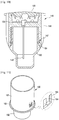
Fig. 1 is a perspective view of a lighting device according to a first embodiment.Fig. 2 is an exploded perspective view of the lighting device shown inFig. 1 .Fig. 3 is a perspective view showing that a light source and a circuitry of the lighting device shown inFig. 1 are separated from each other.Fig. 4 is a bottom perspective view of a heat sink shown inFig. 2 . - Referring to
Figs. 1 to 4 , the lighting device according to the first embodiment may include acover 100, alight source 200, aheat sink 300, acircuitry 400, aninner case 500 and asocket 600. Hereafter, the components will be described in detail respectively. - The
cover 100 has a bulb shape or a hemispherical shape. Thecover 100 has an empty space and a partial opening. - The
cover 100 is coupled to thelight source 200. Specifically, thecover 100 may be coupled to amember 250 of thelight source 200. Thecover 100 may be coupled to themember 250 by using an adhesive or various methods, for example, bolt-fastening, rotary coupling, hook coupling and the like. In the bolt-fastening method, thecover 100 and themember 250 are coupled to each other by using a bolt. In the rotary coupling method, the screw thread of thecover 100 is coupled to the screw groove of themember 250. That is, thecover 100 and themember 250 are coupled to each other by the rotation of thecover 100. In the hook coupling method, thecover 100 and themember 250 are coupled to each other by inserting and fixing the hook (for example, a protrusion, a projection and the like) of thecover 100 into the groove of themember 250. - The
cover 100 is optically coupled to thelight source 200. Specifically, thecover 100 may diffuse, scatter or excite light emitted from thelight source 200. Here, the inner/ outer surface or the inside of thecover 100 may include a fluorescent material so as to excite the light emitted from thelight source 200. - The inner surface of the
cover 100 may be coated with an opalescent pigment. Here, the opalescent pigment may include a diffusing agent diffusing the light. The roughness of the inner surface of thecover 100 may be larger than that of the outer surface of thecover 100. This intends to sufficiently scatter and diffuse the light emitted from thelight source 200. - The
cover 100 may be formed of glass, plastic, polypropylene (PP), polyethylene (PE), polycarbonate (PC) and the like. Here, the polycarbonate (PC) has excellent light resistance, thermal resistance and rigidity. - The
cover 100 may be formed of a transparent material causing thelight source 200 to be visible to the outside or may be formed of an opaque material causing thelight source 200 not to be visible to the outside. - The
cover 100 may be formed by a blow molding process. - The
light source 200 may include at least onelight source module 210 and themember 250. - The
light source module 210 is disposed on themember 250 in such a manner as to emit light to the inner surface of thecover 100. Themember 250 may be coupled to theheat sink 300. Themember 250 coupled to theheat sink 300 is able to electrically connect thelight source module 210 with thecircuitry 400. Hereafter, thelight source module 210 and thecircuitry 400 will be described in detail. - The
light source module 210 includes a substrate 211 and at least one light emittingdevice 215. Thelight emitting device 215 is disposed on one side of the substrate 211. As shown in the drawing, the twolight source modules 210 may be provided. Otherwise, one or more than threelight source modules 210 may be provided. - The substrate 211 may be disposed on the
member 250. - The substrate 211 may have a quadrangular plate shape. However, the substrate 211 may have various shapes without being limited to this. For example, the substrate 211 may have a circular plate shape or a polygonal plate shape. The substrate 211 may be formed by printing a circuit pattern on an insulator. For example, the substrate 211 may include a common printed circuit board (PCB), a metal core PCB, a flexible PCB, a ceramic PCB and the like. Also, the substrate 211 may include a chips on board (COB) allowing an unpackaged LED chip to be directly bonded to a printed circuit board. The substrate 211 may be formed of a material capable of efficiently reflecting light. The surface of the substrate 211 may have a color such as white, silver and the like capable of efficiently reflecting light.
- The surface of the substrate 211 may be coated with a material capable of efficiently reflecting light. The surface of the substrate 211 may be coated with a color capable of efficiently reflecting light, for example, white, silver and the like.
- The
light emitting device 215 may be a light emitting diode chip emitting red, green and blue light or a light emitting diode chip emitting UV. Here, the light emitting diode chip may have a lateral type or vertical type and may emit blue, red, yellow or green light. - The
light emitting device 215 may have a fluorescent material. The fluorescent material may include at least any one selected from a group consisting of a garnet material (YAG, TAG), a silicate material, a nitride material and an oxynitride material. Otherwise, the fluorescent material may include at least any one selected from a group consisting of a yellow fluorescent material, a green fluorescent material and a red fluorescent material. - The
member 250 may include afirst placement portion 251, aguide 253 and asecond placement portion 255. Here, thefirst placement portion 251 may be the top surface of themember 250. Thesecond placement portion 255 may be the bottom surface of themember 250. Thefirst placement portion 251 and thesecond placement portion 255 may be separated by theguide 253. - The
light source module 210 is disposed in thefirst placement portion 251. Specifically, the substrate 211 of thelight source module 210 may be disposed in thefirst placement portion 251. Thefirst placement portion 251 may have a cavity 251-1 into which the substrate 211 may be inserted. The depth of the cavity 251-1 may be the same as the thickness of the substrate 211. A plurality of the cavities 251-1 may be provided according to the number of the substrates 211. - As shown in
Fig. 3 , afirst terminal 270 is disposed in thesecond placement portion 255. Thefirst terminal 270 is a conductor through which electricity flows. - The
first terminal 270 may include a positive (+) electrode and a negative (-) electrode. Here, the positive (+) electrode and the negative (-) electrode are disposed apart from each other. The positive (+) electrode is connected to the positive (+) electrode of asecond terminal 330. The negative (-) electrode is connected to the negative (-) electrode of thesecond terminal 330. - The
first terminal 270 is electrically connected to thelight source module 210 disposed in thefirst placement portion 251. Thefirst terminal 270 may be electrically connected to thelight source module 210 by using a wire. That is, one end of a wire may be connected to thefirst terminal 270. The other end of the wire may be connected to the substrate 211 of thelight source module 210. - The
first terminal 270 may be electrically connected to thelight source module 210 by thefirst terminal 270 itself. That is, one end of thefirst terminal 270 may be connected to the substrate 211 of thelight source module 210. The other end of thefirst terminal 270 may be disposed in thesecond placement portion 255. - The
first terminal 270 directly contacts with thesecond terminal 330 of theheat sink 300. Due to the direct contact between thefirst terminal 270 and thesecond terminal 330, thefirst terminal 270 and thesecond terminal 330 may be electrically connected to each other. - The
guide 253 is disposed between thecover 100 and theheat sink 300. The upper portion of theguide 253 is coupled to thecover 100. The lower portion of theguide 253 is coupled to heat radiatingfins 370 of theheat sink 300. Thefirst placement portion 251 and thesecond placement portion 255 may be separated by theguide 253. - The
second placement portion 255 may be received in afirst receiver 310 of theheat sink 300. When thesecond placement portion 255 is received in thefirst receiver 310, thefirst terminal 270 mechanically contacts with thesecond terminal 330, and then thefirst terminal 270 and thesecond terminal 330 can be electrically connected to each other. - The
member 250 may be formed of a material having thermal conductivity. This intends that themember 250 rapidly receives heat generated from thelight source module 210 and protects thelight source module 210 from the heat. Themember 250 may be formed of, for example, Al, Ni, Cu, Mg, Ag, Sn and the like and an alloy including the metallic materials. Themember 250 may be also formed of thermally conductive plastic. The thermally conductive plastic is lighter than a metallic material and has a unidirectional thermal conductivity. - The
member 250 may include an insulatingportion 290. When themember 250 is made of a metallic material through which electricity flows, since thefirst terminal 270 is also a conductor, electrical short-cut may occur between themember 250 and thefirst terminal 270. The insulatingportion 290 prevents the electrical short-cut. The insulatingportion 290 may be disposed in thesecond placement portion 255 of themember 250 in such a manner as to surround thefirst terminal 270. - The
heat sink 300 receives the heat from thelight source 200 and thecircuitry 400 and radiates the heat. Theheat sink 300 may be formed of Al, Ni, Cu, Mg, Ag, Sn and the like and an alloy including the metallic materials. Theheat sink 300 may be also formed of thermally conductive plastic. The thermally conductive plastic is lighter than a metallic material and has a unidirectional thermal conductivity. - The
heat sink 300 may have thefirst receiver 310 and asecond receiver 350. - The
first receiver 310 may be formed by theheat radiating fins 370 and one side of theheat sink 300. Specifically, thefirst receiver 310 may be determined by oneside 311 of theheat sink 300 and oneside 371 of theheat radiating fin 370. Here, the oneside 311 of theheat sink 300 and the oneside 371 of theheat radiating fin 370 may be inclined with respect to each other or may be substantially perpendicular to each other. - The
first receiver 310 receives thesecond placement portion 255 of themember 250. In this case, since thesecond placement portion 255 directly contacts with the oneside 311 of thefirst receiver 310 and the oneside 371 of theheat radiating fin 370, the heat from themember 250 may be directly transferred to theheat sink 300 and theheat radiating fins 370. - The
second terminal 330 is disposed in thefirst receiver 310. Thesecond terminal 330 is disposed on the oneside 311 of theheat sink 300. Thesecond terminal 330 is a conductor and directly contacts with thefirst terminal 270 of themember 250. Therefore, thesecond terminal 330 is electrically connected to thefirst terminal 270. - Like the
first terminal 270, thesecond terminal 330 may include a positive (+) electrode and a negative (-) electrode. The positive (+) electrode and the negative (-) electrode are disposed apart from each other. The positive (+) electrode is connected to the positive (+) electrode of thefirst terminal 270. The negative (-) electrode is connected to the negative (-) electrode of thefirst terminal 270. - The
second receiver 350 is disposed corresponding to thefirst receiver 310 of theheat sink 300. Thefirst receiver 310 is disposed on thesecond receiver 350. Contrarily, thesecond receiver 350 is disposed under thefirst receiver 310. - The
second receiver 350 may be a cavity formed in the other side of theheat sink 300. Thesecond receiver 350 has a predetermined depth in the direction of thefirst receiver 310. The depth of thesecond receiver 350 may be greater than that of thefirst receiver 310. The depth of thesecond receiver 350 may be changed according to the size of thecircuitry 400. - The
second receiver 350 receives thecircuitry 400 and theinner case 500. Specifically, theinner case 500 receives thecircuitry 400, and then thesecond receiver 350 receives theinner case 500. - The
heat sink 300 may have theheat radiating fins 370. Theheat radiating fins 370 may extend from or may be connected to the outer surface of theheat sink 300. Theheat radiating fins 370 increase the heat radiating area of theheat sink 300, thereby improving heat radiation efficiency. - The one
side 371 of theheat radiating fin 370, together with the oneside 311 of theheat sink 300 can determine thefirst receiver 310. - The
guide 253 of themember 250 is disposed on theheat radiating fins 370. Theheat radiating fins 370 are able to directly receive heat from theguide 253. - The
heat sink 300 may include an insulatingportion 390. When theheat sink 300 is made of a metallic material through which electricity flows, since thesecond terminal 330 is also a conductor, electrical short-cut may occur between theheat sink 300 and thesecond terminal 330. The insulatingportion 390 prevents the electrical short-cut. The insulatingportion 390 may be disposed on the oneside 311 of theheat sink 300 in such a manner as to surround thesecond terminal 330. - The
circuitry 400 receives external electric power, and then converts the received electric power in accordance with thelight source module 210 of thelight source 200. Thecircuitry 400 supplies the converted electric power to thelight source 200. - The
circuitry 400 is received in theheat sink 300. Specifically, thecircuitry 400 is received in theinner case 500, and then, together with theinner case 500, is received in thesecond receiver 350 of theheat sink 300. - The
circuitry 400 may include acircuit board 410 and a plurality ofparts 430 mounted on thecircuit board 410. - The
circuit board 410 may have a quadrangular plate shape. However, thecircuit board 410 may have various shapes without being limited to this. For example, thecircuit board 410 may have an elliptical plate shape or a circular plate shape. Thecircuit board 410 may be formed by printing a circuit pattern on an insulator. Thecircuit board 410 may include a metal core PCB, a flexible PCB, a ceramic PCB and the like. - The
circuit board 410 is electrically connected to thesecond terminal 330 of theheat sink 300. Thecircuit board 410 may be electrically connected to thesecond terminal 330 by using a wire. That is, one end of a wire may be connected to thesecond terminal 330. The other end of the wire may be connected to thecircuit board 410. - The
circuit board 410 may be electrically connected to thesecond terminal 330 by thesecond terminal 330 itself. That is, one end of thesecond terminal 330 may be directly connected to thecircuit board 410. The other end of thesecond terminal 330 may be, as shown inFig. 2 , disposed on the oneside 311 of theheat sink 300. - The plurality of
parts 430 may include, for example, a Converter converting AC power supply supplied by an external power supply into DC power supply, a driving chip controlling the driving of thelight source module 210, and an electrostatic discharge (ESD) protective device for protecting thelight source module 210. - The
inner case 500 receives thecircuitry 400 thereinside. Theinner case 500 may have areceiver 510 for receiving thecircuitry 400. Thereceiver 510 may have a cylindrical shape. The shape of thereceiver 510 may be changed according to the shape of thesecond receiver 350 of theheat sink 300. - The
inner case 500 is received in theheat sink 300. Thereceiver 510 of theinner case 500 is received in thesecond receiver 350 of theheat sink 300. - The
inner case 500 is coupled to thesocket 600. Theinner case 500 may include aconnection portion 530 which is coupled to thesocket 600. Theconnection portion 530 may have a screw thread corresponding to the screw groove of thesocket 600. The diameter of theconnection portion 530 may be less than that of thereceiver 510. - The
inner case 500 is a nonconductor. Therefore, theinner case 500 prevents electrical short-cut between thecircuitry 400 and theheat sink 300. Theinner case 500 may be made of a plastic or resin material. - The
socket 600 is coupled to theinner case 500. Specifically, thesocket 600 is coupled to theconnection portion 530 of theinner case 500. - The
socket 600 may have the same structure as that of a conventional incandescent bulb. Thecircuitry 400 is electrically connected to thesocket 600. Thecircuitry 400 may be electrically connected to thesocket 600 by using a wire. Therefore, when external electric power is applied to thesocket 600, the external electric power may be transmitted to thecircuitry 400. - The
socket 600 may have a screw groove corresponding to the screw thread of theconnection portion 530. -
Fig. 5 is a view showing modified examples of the first terminal and the second terminal, each of which is shown inFigs. 2 and3 respectively. - Terminals 270' and 330' shown in
Fig. 5 are modified examples of thesecond terminal 330 shown inFig. 2 and thefirst terminal 270 shown inFig. 3 . - Referring to
Fig. 5 , each of the first and the second terminals 270' and 330' may include a circular negative (-) electrode and a positive (+) electrode surrounding the negative (-) electrode. Contrarily, each of the first and the second terminals 270' and 330' may include a circular positive (+) electrode and a negative (-) electrode surrounding the positive (+) electrode. - Though not shown separately in the drawing, the
second terminal 330 shown inFig. 2 and thefirst terminal 270 shown inFig. 3 may have a shape which is inserted and fitted like a battery or may have a protruding shape which can be pushed inwardly. -
Fig. 6 is a perspective view showing a modified example of the lighting device shown inFig. 2 . - In description of the lighting device according to the modified example shown in
Fig. 6 , only differences between the lighting device shown inFig. 6 and the lighting device shown inFigs. 1 to 4 will be described. - A light source 200' has a
screw thread 255a'. Specifically, thescrew thread 255a' may be disposed on a second placement portion 255' of a member 250'. More specifically, thescrew thread 255a' may be disposed on the lateral surface of the second placement portion 255'. - The light source 200' includes the first terminal 270' shown in
Fig. 5 . - A heat sink 300' has a first receiver 310'. The first receiver 310' may be a cavity which is determined by the lateral surface 313' and bottom surface 311' of the heat sink 300'.
- The heat sink 300' has a
screw groove 313a'. Thescrew groove 313a' is coupled to thescrew thread 255a' of the light source 200'. Thescrew groove 313a' may be disposed on the lateral surface 313' of the first receiver 310'. - The heat sink 300' includes the second terminal 330' shown in
Fig. 5 . The second terminal 330' may be disposed on the bottom surface 311' of the heat sink 300'. - In the lighting device shown in
Fig. 6 , the light source 200' and the heat sink 300' can be easily coupled to or separated from each other by rotating them through the use of thescrew thread 255a' and thescrew groove 313a'. Also, since the lighting device shown inFig. 6 includes the first and the second terminals 270' and 330' shown inFig. 5 , the light source 200' and the heat sink 300' can be easily electrically connected to each other without distinguishing between the positive (+) electrode and the negative (-) electrode. -
Fig. 7 is a view showing another modified example of the lighting device shown inFig. 2 . - In description of the lighting device according to the another modified example shown in
Fig. 7 , only differences between the lighting device shown inFig. 7 and the lighting device shown inFigs. 1 to 4 will be described. - A
light source 200" has a catchingprojection 253a". The catchingprojection 253a" may be disposed on aguide 253" of amember 250". Specifically, the catchingprojection 253a" may project from theguide 253" toward aheat sink 300". - The
second placement portion 255" of thelight source 200" includes the first terminal 270' shown inFig. 5 . However, the first terminal 270' may be thefirst terminal 270 shown inFig. 3 without being limited to this. - The
heat sink 300" has atap 320". Afirst receiver 310" may be determined by thetap 320" and oneside 311" of theheat sink 300". - The
tap 320" has a catchinggroove 320a". The catchingprojection 253a" of thelight source 200" is inserted into the catchinggroove 320a". - The number of the catching
grooves 320a" may correspond to the number of the catchingprojections 253a". - The
heat sink 300" includes the second terminal 330' shown inFig. 5 . However, the second terminal 330' may be thesecond terminal 330 shown inFig. 2 without being limited to this. - In the lighting device shown in
Fig. 7 , thelight source 200" and theheat sink 300" can be easily coupled to or separated from each other by using the catchingprojection 253a" and the catchinggroove 320a". Also, since the lighting device shown inFig. 7 includes the first and the second terminals 270' and 330' shown inFig. 5 , thelight source 200" and theheat sink 300" can be easily electrically connected to each other without distinguishing between the positive (+) electrode and the negative (-) electrode. -
Fig. 8 is a view showing further another modified example of the lighting device shown inFig. 2 . - In description of the lighting device according to the further another modified example shown in
Fig. 8 , only differences between the lighting device shown inFig. 8 and the lighting device shown inFig. 7 will be described. - A
light source 200"' has a catchingprojection 255a"'. The catchingprojection 255a"' may be disposed on asecond placement portion 255"' of amember 250"'. Specifically, the catchingprojection 255a"' may project from the lateral surface of thesecond placement portion 255"'. Also, the catchingprojection 255a"' may project from thesecond placement portion 255"' perpendicularly to a direction in which thelight source 200"' is coupled to aheat sink 300"'. - The
light source 200"' includes the first terminal 270' shown inFig. 5 . However, the first terminal 270' may be thefirst terminal 270 shown inFig. 3 without being limited to this. - The
heat sink 300"' has a catchinggroove 320a"'. The catchingprojection 255a"' is inserted into the catchinggroove 320a"'. The catchinggroove 320a"' may be bent in the form of "L". As the catchingprojection 255a"' moves along the "L"-shaped catchinggroove 320a"', thelight source 200"' may be coupled to theheat sink 300"'. - The number of the catching
grooves 320a"' may correspond to the number of the catchingprojections 255a"'. - The
heat sink 300"' includes the second terminal 330' shown inFig. 5 . However, the second terminal 330' may be thesecond terminal 330 shown inFig. 2 without being limited to this. - In the lighting device shown in
Fig. 8 , thelight source 200"' and theheat sink 300"' can be easily coupled to or separated from each other by using the catchingprojection 255a" and the catchinggroove 320a"'. Also, since the lighting device shown inFig. 8 includes the first and the second terminals 270' and 330' shown inFig. 5 , thelight source 200"' and theheat sink 300"' can be easily electrically connected to each other without distinguishing between the positive (+) electrode and the negative (-) electrode. -
Fig. 9 is an exploded perspective view of a lighting device according to a second embodiment. - Referring to
Fig. 9 , the lighting device according to the second embodiment may include acover 110, alight source module 130, aheat sink 140, acircuitry 150, aninner case 160 and asocket 170. In the lighting device according to the second embodiment, theheat sink 140 and theinner case 160 are coupled to each other by a hook coupling method. - The
cover 110 is the same as thecover 100 shown inFig. 1 except for the fact that thecover 110 is directly coupled to theheat sink 140. Therefore, the detailed descriptions of the same parts as those of the aforementioned embodiment will be omitted. - The
light source module 130 is the same as thelight source module 210 shown inFig. 1 except for the fact that thelight source module 130 is disposed on theheat sink 140. Specifically, thelight source module 130 includes asubstrate 131 and alight emitting device 132. Thesubstrate 131 is the same as the substrate 211 shown inFig. 1 . Thelight emitting device 132 is the same as thelight emitting device 215 shown inFig. 1 . - The
heat sink 140 may be formed of Al, Ni, Cu, Mg, Ag, Sn and the like and an alloy including the metallic materials. Theheat sink 140 may be also formed of thermally conductive plastic. The thermally conductive plastic is lighter than a metallic material and has a unidirectional thermal conductivity. - The
heat sink 140 is able to improve heat radiation efficiency by coming in surface contact with thelight source module 130. Here, theheat sink 140 and thelight source module 130 may be coupled to each other to come in surface contact with each other by using a structure like a screw, or may be coupled to each other by using an adhesive. - The
heat sink 140 has aflat portion 141 including afirst base 141a and asecond base 141b. Here, a level difference is formed between thefirst base 141a and thesecond base 141b. Each of thefirst base 141a and thesecond base 141b has a flat plate shape. Thesecond base 141b has aseating portion 142 formed therein. Thelight source module 130 is installed in theseating portion 142. Aguide 143 is formed on the upper circumference of theheat sink 140. A recess (not shown) into which thecover 110 is inserted is formed between theguide 143 and thefirst base 141a. - A plurality of
heat radiating fins 144 are formed on the outer surface of theheat sink 140. Theheat radiating fins 144 may extend from or may be connected to the outer surface of theheat sink 140. Theheat radiating fins 144 increase the heat radiating area of thetotal heat sink 140, thereby improving heat radiation efficiency. - The lower inside of the
heat sink 140 has a receiver for receiving theinner case 160. The receiver may be a predetermined space. The receiver may be a recess or a groove which has a predetermined depth. - An insertion recess (not shown, see
reference numeral 147 ofFig. 10 ) is formed within a receiver of theinner case 160, that is, in the inner surface defining the receiver of theinner case 160. A hook (seereference numeral 164 ofFig. 11 ) of theinner case 160 is inserted into the insertion recess, so that theinner case 160 is fixed to theheat sink 140. - The
inner case 160 is disposed within the lower portion of theheat sink 140 and is coupled to thesocket 170. Thecircuitry 150 is received in theinner case 160. Thecircuitry 150 controls the power of thelight source module 130 through the electrode terminal of thelight source module 130. - As shown in
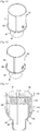
Fig. 11 , theinner case 160 includes thereceiver 161, aconnection portion 162 and a level-difference portion 163. Thereceiver 161 has a cylindrical shape. Theconnection portion 162 is formed under thereceiver 161 in such a manner as to have a diameter less than that of thereceiver 161. The level-difference portion 163 connects thereceiver 161 with theconnection portion 162. - The
inner case 160 may include thehook 164. Specifically, thehook 164 may be formed on both sides of the outer surface of thereceiver 161. When theinner case 160 is disposed within the lower portion of theheat sink 140, thehook 164 is coupled to the insertion recess (seereference numeral 147 ofFig. 10 ) formed within theheat sink 140. - The
inner case 160 may be variously changed as shown inFigs. 11 to 13 . Detailed descriptions of the modified examples of theinner case 160 will be provided inFigs. 11 to 13 . - The
inner case 160 may be formed of a nonconductor in order to prevent electrical short-cut between thecircuitry 150 and theheat sink 140. Theinner case 160 may be made of a plastic or resin material. - The
circuitry 150 receives electric power from thesocket 170 coupled to the lower portion of theinner case 160 and supplies the electric power to thelight source module 130. - The
circuitry 150 converts the received electric power in accordance with the driving voltage of thelight emitting module 130, and then supplies the converted electric power to thelight source 130. For this purpose, thecircuitry 150 includes aConverter 153 which is disposed on asubstrate 151 and converts AC power supply supplied through thesocket 170 into DC power supply, a driving chip which controls the driving of thelight source module 130, and an electrostatic discharge (ESD) protective device for protecting thelight source module 130. - The
socket 170 is coupled to theinner case 160 and supplies electric power to thecircuitry 150. Thesocket 170 functions to support the lighting device. Like a socket of an incandescent bulb, a screw thread and a screw groove are formed on the outer surface of thesocket 170. Thesocket 170 is coupled to theinner case 160, and then is electrically connected to thecircuitry 150. Here, thesocket 170 may be connected to thecircuitry 150 through a wire or may be directly connected to thecircuitry 150. - In the lighting device according to the second embodiment, the
hook 164 formed on both sides of the outer surface of theinner case 160 is coupled to the insertion recess formed within theheat sink 140. Accordingly, it is possible to overcome defects caused by the destruction of a tap when a bolt is fastened to conventional power supply unit (PSU) housings of MR and PAR products and to overcome defects caused by crack. Here, the PSU is designated to include theheat sink 140 and theinner case 160 receiving thecircuitry 150 therewithin. -
Fig. 10 is an inner cross sectional view of a lighting device according to a third embodiment. - Like the lighting device according to the second embodiment shown in
Fig. 9 , in the lighting device according to the third embodiment shown inFig. 10 , when theinner case 160 is inserted into the inside of the lower portion of theheat sink 140, thehook 164 of theinner case 160 is coupled to theinsertion recess 147 formed within theheat sink 140. However, the lighting device according to the third embodiment shown inFig. 10 is different from the lighting device according to the second embodiment shown inFig. 9 in that thelight source module 130 is disposed within the upper portion of theheat sink 140, and alens 120 is disposed on thelight source module 130. - Here, an
undescribed reference numeral 144 represents a heat radiating fin formed on the outer surface of theheat sink 140. Anundescribed reference numeral 150 represents a circuitry received in theinner case 160. -
Fig. 11 is a perspective view showing only an inner case shown inFig. 9 . - Referring to
Fig. 11 , theinner case 160 includes thereceiver 161, theconnection portion 162 and the level-difference portion 163. Thereceiver 161 has a cylindrical shape. Theconnection portion 162 is formed under thereceiver 161 in such a manner as to have a diameter less than that of thereceiver 161. The level-difference portion 163 connects thereceiver 161 with theconnection portion 162. - Here, the
hook 164 is integrally formed on both sides of the outer surface of thereceiver 161. Specifically, thehook 164 may be disposed on the lower portion of the outer surface of thereceiver 161. However, thehook 164 may be disposed on the upper or central portion of the outer surface of thereceiver 161 without being limited to this. - The
hook 164 may be disposed in anopening 165 formed in the outer surface of theinner case 160. Specifically, thehook 164 may extend toward theopening 165 of theinner case 160. Thehook 164 may project in such a manner that the end of thehook 164 is inclined. - When the
inner case 160 is disposed within the lower portion of theheat sink 140, thehook 164 is coupled to the insertion recess formed within theheat sink 140. Therefore, theinner case 160 can be fixed to theheat sink 140 by the coupling of thehook 164 and the insertion recess. - The
hook 164 formed on both sides of the outer surface of theinner case 160 is coupled to the insertion recess formed within theheat sink 140. Accordingly, it is possible to overcome defects caused by the destruction of a tap when a bolt is fastened to conventional power supply unit (PSU) housings of MR, PAR and a general bulb product and to overcome defects caused by crack. -
Fig. 12 is a perspective view showing a first modified example of the inner case shown inFig. 11 . - Referring to
Fig. 12 , like theinner case 160 shown inFig. 11 , an inner case 160' includes thereceiver 161, theconnection portion 162 and the level-difference portion 163. Here, the inner case 160' shown inFig. 12 further includes aguide projection 167. - The
guide projection 167 may project from the outer surface of thereceiver 161 and may be formed in the longitudinal direction of thereceiver 161. - The
guide projection 167 may have a hemispherical shape. However, theguide projection 167 may have a polygonal shape including a triangular shape, a quadrangular shape and the like. - The
guide projection 167 may be inserted into a guide groove (not shown) formed within the heat sink (seereference numeral 140 ofFig. 9 ) in a sliding manner. Here, the guide groove (not shown) of theheat sink 140 is formed at a position corresponding to the position of theguide projection 167 of the inner case 160'. The guide groove (not shown) of theheat sink 140 may have a shape corresponding to the shape of theguide projection 167 of the inner case 160'. As such, theguide projection 167 may function to indicate a direction in which the inner case 160' and theheat sink 140 are coupled to each other and where the inner case 160' and theheat sink 140 are coupled to each other. - When the
guide projection 167 formed on the outer surface of the inner case 160' is inserted in a sliding manner into the guide groove (not shown) formed within theheat sink 140, thehook 164 formed on both sides of the outer surface of the inner case 160' is automatically coupled to the insertion recess formed within theheat sink 140. Accordingly, it is possible to overcome defects caused by the destruction of a tap when a bolt is fastened to conventional power supply unit (PSU) housings of MR, PAR and a general bulb product and to overcome defects caused by crack. -
Fig. 13 is a perspective view showing a second modified example of the inner case shown inFig. 11 . - Referring to
Fig. 13 , like theinner case 160 shown inFig. 11 , aninner case 160" includes thereceiver 161, theconnection portion 162 and the level-difference portion 163. Here, theinner case 160" shown inFig. 13 further includes a guide groove 167'. - The guide groove 167' may be formed toward the inside of the
receiver 161 in the longitudinal direction of thereceiver 161. - The guide groove 167' may have a hemispherical shape. However, the
guide projection 167 may have a polygonal shape including a triangular shape, a quadrangular shape and the like. - The guide groove 167' may be inserted into a guide projection (not shown) formed within the heat sink (see
reference numeral 140 ofFig. 9 ) in a sliding manner. Here, the guide projection (not shown) of theheat sink 140 is formed at a position corresponding to the position of the guide groove 167' of theinner case 160". The guide projection (not shown) of theheat sink 140 may have a shape corresponding to the shape of the guide groove 167' of theinner case 160". As such, the guide groove 167' may function to indicate a direction in which theinner case 160" and theheat sink 140 are coupled to each other and where theinner case 160" and theheat sink 140 are coupled to each other. - When the guide groove 167' formed on the outer surface of the
inner case 160" is inserted in a sliding manner into the guide projection (not shown) formed within theheat sink 140, thehook 164 formed on both sides of the outer surface of theinner case 160" is automatically coupled to the insertion recess formed within theheat sink 140. Accordingly, it is possible to overcome defects caused by the destruction of a tap when a bolt is fastened to conventional power supply unit (PSU) housings of MR and PAR products and to overcome defects caused by crack. -
Fig. 14 is an inner cross sectional view of the lighting device according to the second embodiment shown inFig. 9 .Fig. 15 is a perspective view of the inner case shown inFig. 9 which is turned upside down. - Referring to
Figs. 9 ,14 to 15 , theinner case 160 includes aninlet 166. Theinlet 166 is a hole for injecting molding liquid to heat generating parts received within theinner case 160. Theinlet 166 may be formed in the level-difference portion 163. - The
circuitry 150 is received within theinner case 160.Molding liquid 210 is cured and then disposed around theConverter 153 of thecircuitry 150. Since theConverter 153 generates heat from the operation thereof, themolding liquid 210 surrounds theConverter 153 for the purpose of protecting other circuits from the generated heat and radiating the heat. - The
Converter 153 may be an AC-DC converter which changes a value of alternating current voltage or a value of alternating current. - The
molding liquid 210 is injected only around the internal heat generating parts, i.e., theConverter 153 through theinlet 166 formed in theinner case 160, and then is cured. Through this, a manufacturing cost can be reduced by reducing the amount of the molding liquid used. - More specifically, in the past, the
molding liquid 210 was filled in the entire inside of theinner case 160 through the opening of theinner case 160. As a result, a molding process was also performed on portions requiring no molding liquid. However, in the embodiment, after arubber cover 200 is coupled to the opening of theinner case 160, themolding liquid 210 is injected into only theConverter 153 through theinlet 166 and is cured, so that the amount of the molding liquid used can be reduced. -
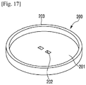
Fig. 16 is a cross sectional view showing that the molding liquid is injected into the heat generating parts of the circuitry through the inlet of the inner case.Fig. 17 is a perspective view of the rubber cover used to inject the molding liquid through the inlet of the inner case. - The
inner case 160 includes thereceiver 161, theconnection portion 162 and the level-difference portion 163. Here, the level-difference portion 163 is an inclined portion. Theinlet 166 is formed in theinclined portion 163. - The
inlet 166 is formed in theinclined portion 163 of theinner case 160 so as to surround only theConverter 153 by themolding liquid 210. Further, for the sake of preventing the leakage of themolding liquid 210 being injected, therubber cover 200 is provided in the opening of thereceiver 161 of theinner case 160 in the form of JIG. After themolding liquid 210 is injected into theinner case 160 and is cured, therubber cover 200 is removed. - The
rubber cover 200 includes aflat portion 201 and aborder wall 203. Theflat portion 201 has a flat circular shape. Theborder wall 203 projects from the outer circumference of theflat portion 201 and is coupled to the outer surface of thereceiver 161. Arecess 202 is formed in theflat portion 201. When therubber cover 200 is coupled to the opening of thereceiver 161, the projecting portion of thecircuitry 150 is inserted into therecess 202. - A method for injecting the
molding liquid 210 into the inside of theinner case 160 by using therubber cover 200 and theinner case 160 having theinlet 166 formed therein will be described. - First, the
rubber cover 200 is coupled to the opening of thereceiver 161 of theinner case 160. Then, theinner case 160 is installed such that theinlet 166 faces upward (seeFig. 16 ). Here, the heat generating parts received within theinner case 160, i.e., theConverter 153 is, as shown inFig. 16 , positioned in the lower portion of theinner case 160. - Then, the
molding liquid 210 is injected through theinlet 166 of theinner case 160. Here, themolding liquid 210 is injected in such a manner as to sufficiently cover only the heat generating parts including theConverter 153, which are received within theinner case 160. - Lastly, the
molding liquid 210 is cured and then therubber cover 200 is removed. - In the foregoing molding method, after the
molding liquid 200 injected through theinlet 166 is cured, theinlet 166 may be sealed by being molded with silicone or resin material. - As such, in the lighting device according to the second embodiment, the
inlet 166 used to inject themolding liquid 210 into theinner case 160 is formed and the molding liquid is injected into only the heat generating parts. Through this, a manufacturing cost can be reduced. Also, therubber cover 200 is provided in the form of JIG and removed after the molding liquid is cured. As a result, a manufacturing cost can be reduced by removing the parts. - Although embodiments of the present invention were described above, these are just examples and do not limit the present invention. Further, the present invention may be changed and modified in various ways, without departing from the essential features of the present invention, by those skilled in the art. For example, the components described in detail in the embodiments of the present invention may be modified. Further, differences due to the modification and application should be construed as being included in the scope of the present invention, which is described in the accompanying claims.
Claims (9)
- A lighting device comprising:a light source module (130);a heat sink (140) in which the light source module is disposed and that has a receiver;an inner case (160) disposed in the receiver of the heat sink and having at least one inlet (166) for injecting molding liquid,a circuitry (150) disposed within the inner case, the circuitry supplying electric power to the light source module, and the circuitry including heat generating parts (153);a socket (170) which is coupled to the inner case (160) and supplied electric power to the circuitry (150),characterized in that:the inner case (160) includes:a cylindrical receiver (161) having an opening;a connection portion (162) disposed under the cylindrical receiver and having a diameter less than a diameter of the cylindrical receiver, andan inclined portion (163) connecting the cylindrical receiver with the connection portion,the lighting device comprises a cured molding liquid (210) which is disposed from the opening of the cylindrical receiver (161) to a predetermined height so that the heat generating parts are covered, andthe cured molding liquid (210) is not disposed over an entire inside of the inner case (160), characterised in that the inlet for injecting molding liquid is provided in the inclined portion.
- The lighting device of claim 1, further comprising a silicone or resin material sealing the inlet for injecting molding liquid.
- The lighting device of any one claim of claims 1 to 2, wherein the heat sink has an insertion recess (147), and wherein the inner case has a hook (164) coupled to the insertion recess.
- The lighting device of claim 3, wherein the hook (164) is disposed in an opening (165) disposed at the outer surface of the inner case.
- The lighting device of claim 4, wherein the hook extends towards the opening of the inner case, and wherein the hook projects in such a manner that the end of the hook is inclined.
- The lighting device of any one claim of claims 3 to 5, wherein heat sink (140) includes a flat portion (141) including a first base (141a) and a second base (141b), wherein the second base has a seating portion (142) formed therein, and wherein the light source module is disposed in the seating portion.
- The lighting device of any one claim of claims 1 to 6, wherein the inner case is formed of a nonconductor in order to prevent electrical short-cut between the circuitry and the heat sink.
- The lighting device of any one claim of claims 1 to 7, wherein the circuitry includes a substrate (151) on which the heat generating parts is disposed.
- The lighting device of any one claim of claims 1 to 8, wherein the heat generating parts is a converter converting AC power supply into DC power supply.
Applications Claiming Priority (5)
| Application Number | Priority Date | Filing Date | Title |
|---|---|---|---|
| KR1020110085481A KR101304874B1 (en) | 2011-08-26 | 2011-08-26 | Lighting device |
| KR1020110117253A KR20130052051A (en) | 2011-11-11 | 2011-11-11 | Lighting device |
| KR1020110117254A KR101834865B1 (en) | 2011-11-11 | 2011-11-11 | Lighting device and manufacture method of the same |
| EP12827351.3A EP2748513B1 (en) | 2011-08-26 | 2012-08-24 | Lighting device |
| PCT/KR2012/006764 WO2013032181A2 (en) | 2011-08-26 | 2012-08-24 | Lighting device |
Related Parent Applications (2)
| Application Number | Title | Priority Date | Filing Date |
|---|---|---|---|
| EP12827351.3A Division EP2748513B1 (en) | 2011-08-26 | 2012-08-24 | Lighting device |
| EP12827351.3A Division-Into EP2748513B1 (en) | 2011-08-26 | 2012-08-24 | Lighting device |
Publications (2)
| Publication Number | Publication Date |
|---|---|
| EP3179152A1 EP3179152A1 (en) | 2017-06-14 |
| EP3179152B1 true EP3179152B1 (en) | 2020-03-18 |
Family
ID=47757029
Family Applications (2)
| Application Number | Title | Priority Date | Filing Date |
|---|---|---|---|
| EP16204859.9A Active EP3179152B1 (en) | 2011-08-26 | 2012-08-24 | Lighting device |
| EP12827351.3A Active EP2748513B1 (en) | 2011-08-26 | 2012-08-24 | Lighting device |
Family Applications After (1)
| Application Number | Title | Priority Date | Filing Date |
|---|---|---|---|
| EP12827351.3A Active EP2748513B1 (en) | 2011-08-26 | 2012-08-24 | Lighting device |
Country Status (4)
| Country | Link |
|---|---|
| EP (2) | EP3179152B1 (en) |
| JP (1) | JP6196218B2 (en) |
| CN (1) | CN103765078A (en) |
| WO (1) | WO2013032181A2 (en) |
Families Citing this family (5)
| Publication number | Priority date | Publication date | Assignee | Title |
|---|---|---|---|---|
| CN104266098B (en) * | 2014-10-10 | 2017-04-05 | 东莞市驰明电子科技有限公司 | Light fixture |
| CN108105726A (en) * | 2014-11-28 | 2018-06-01 | 欧普照明股份有限公司 | A kind of lamp fixing device |
| CN107975767A (en) * | 2014-11-28 | 2018-05-01 | 欧普照明股份有限公司 | A kind of lamps and lanterns fixed seat and light fitting connecting seat and a kind of lamp fixing device |
| JP2016167436A (en) * | 2015-03-10 | 2016-09-15 | パナソニックIpマネジメント株式会社 | Light source for illumination and lighting device |
| CN105042360A (en) * | 2015-06-25 | 2015-11-11 | 吴静 | Easily-assembled LED bulb lamp |
Family Cites Families (25)
| Publication number | Priority date | Publication date | Assignee | Title |
|---|---|---|---|---|
| US2477901A (en) * | 1948-04-07 | 1949-08-02 | Nathan M Robboy | Swivel fixture joint |
| JP3455900B2 (en) * | 1999-05-25 | 2003-10-14 | 日本航空電子工業株式会社 | Electrical connection structure |
| JP2003217311A (en) * | 2002-01-28 | 2003-07-31 | Toshiba Lighting & Technology Corp | Bulb shaped fluorescent lamp |
| JP2006093044A (en) * | 2004-09-27 | 2006-04-06 | Toshiba Lighting & Technology Corp | Bulb-shaped fluorescent lamp and lighting apparatus |
| JP4725231B2 (en) * | 2005-04-08 | 2011-07-13 | 東芝ライテック株式会社 | Light bulb lamp |
| ES2855400T3 (en) * | 2005-05-23 | 2021-09-23 | Signify North America Corp | Modular lighting fixture based on LEDs for the coupling of sockets, lighting accessories that incorporate them and procedures for their assembly, installation and removal. |
| US7766518B2 (en) | 2005-05-23 | 2010-08-03 | Philips Solid-State Lighting Solutions, Inc. | LED-based light-generating modules for socket engagement, and methods of assembling, installing and removing same |
| JP2007265892A (en) * | 2006-03-29 | 2007-10-11 | Yuki Enterprise:Kk | Bulb type led lamp |
| KR100759054B1 (en) * | 2006-11-01 | 2007-09-14 | 박청용 | Led light |
| EP2163808B1 (en) * | 2007-05-23 | 2014-04-23 | Sharp Kabushiki Kaisha | Lighting device |
| JP4980152B2 (en) * | 2007-06-19 | 2012-07-18 | シャープ株式会社 | Lighting device |
| JP5029893B2 (en) * | 2007-07-06 | 2012-09-19 | 東芝ライテック株式会社 | Light bulb shaped LED lamp and lighting device |
| JP4569683B2 (en) * | 2007-10-16 | 2010-10-27 | 東芝ライテック株式会社 | Light emitting element lamp and lighting apparatus |
| KR100908136B1 (en) * | 2007-12-27 | 2009-07-16 | 홍삼표 | Led lamp |
| US7866850B2 (en) * | 2008-02-26 | 2011-01-11 | Journée Lighting, Inc. | Light fixture assembly and LED assembly |
| CN102175000B (en) * | 2008-07-30 | 2013-11-06 | 东芝照明技术株式会社 | Lamp and lighting equipment |
| JP2010061852A (en) * | 2008-09-01 | 2010-03-18 | Panasonic Corp | Lamp, circuit unit and light source unit |
| CN101676602A (en) * | 2008-09-19 | 2010-03-24 | 东芝照明技术株式会社 | Lamp device and lighting apparatus |
| FR2938047A1 (en) | 2008-10-31 | 2010-05-07 | Mpe Solutions | Light source, has LED support connected with case by detachable connection device that includes electric connector and thermal connector, where thermal connector includes male and female parts |
| KR20100007038U (en) * | 2008-12-31 | 2010-07-08 | (주)카인스 | The LED light bulb |
| WO2011025928A2 (en) * | 2009-08-28 | 2011-03-03 | Firefly Led Lighting Inc. | Lighting system with replaceable illumination module |
| US8154179B2 (en) * | 2009-12-09 | 2012-04-10 | Tsan-Chi Chen | Light emitting diode lamp having replaceable light source module |
| JP5508113B2 (en) * | 2010-04-21 | 2014-05-28 | パナソニック株式会社 | Lamp and lighting device |
| DE102010028481A1 (en) * | 2010-05-03 | 2011-11-03 | Osram Gesellschaft mit beschränkter Haftung | Electronic housing for a lamp, semiconductor lamp and method for casting an electronics housing for a lamp |
| CN201731336U (en) * | 2010-07-02 | 2011-02-02 | 厦门龙胜达照明电器有限公司 | LED lamp |
-
2012
- 2012-08-24 CN CN201280041615.8A patent/CN103765078A/en active Pending
- 2012-08-24 EP EP16204859.9A patent/EP3179152B1/en active Active
- 2012-08-24 EP EP12827351.3A patent/EP2748513B1/en active Active
- 2012-08-24 WO PCT/KR2012/006764 patent/WO2013032181A2/en active Application Filing
- 2012-08-24 JP JP2014527078A patent/JP6196218B2/en active Active
Non-Patent Citations (1)
| Title |
|---|
| None * |
Also Published As
| Publication number | Publication date |
|---|---|
| EP3179152A1 (en) | 2017-06-14 |
| CN103765078A (en) | 2014-04-30 |
| JP2014525652A (en) | 2014-09-29 |
| JP6196218B2 (en) | 2017-09-13 |
| WO2013032181A2 (en) | 2013-03-07 |
| WO2013032181A3 (en) | 2013-04-25 |
| EP2748513A2 (en) | 2014-07-02 |
| EP2748513B1 (en) | 2017-02-08 |
| EP2748513A4 (en) | 2015-05-06 |
Similar Documents
| Publication | Publication Date | Title |
|---|---|---|
| US10024515B2 (en) | Lighting device having separable light source and circuitry | |
| KR101827717B1 (en) | Lighting device | |
| EP3179152B1 (en) | Lighting device | |
| EP2753873B1 (en) | Lighting device | |
| KR101315703B1 (en) | Lighting device | |
| KR101103525B1 (en) | Lighting device | |
| KR101103524B1 (en) | Lighting device | |
| KR101834865B1 (en) | Lighting device and manufacture method of the same | |
| KR101879215B1 (en) | Light Source Segregation Type Lighting Device | |
| KR102031737B1 (en) | Lighting device | |
| KR102089625B1 (en) | Lighting device | |
| KR101304874B1 (en) | Lighting device | |
| KR102079971B1 (en) | Lighting device | |
| KR101920231B1 (en) | Lighting device | |
| KR101847048B1 (en) | Lighting device | |
| KR101859439B1 (en) | Lighting device | |
| KR20120061428A (en) | Lighting device | |
| KR102014174B1 (en) | Lighting device | |
| KR101846396B1 (en) | Lighting device | |
| KR102076007B1 (en) | Lighting device | |
| KR102024704B1 (en) | Lighting device | |
| KR20130134754A (en) | Illuminating lamp | |
| KR102050354B1 (en) | Lighting device | |
| KR102066102B1 (en) | Lighting device | |
| KR101847045B1 (en) | Lighting device |
Legal Events
| Date | Code | Title | Description |
|---|---|---|---|
| PUAI | Public reference made under article 153(3) epc to a published international application that has entered the european phase |
Free format text: ORIGINAL CODE: 0009012 |
|
| STAA | Information on the status of an ep patent application or granted ep patent |
Free format text: STATUS: THE APPLICATION HAS BEEN PUBLISHED |
|
| AC | Divisional application: reference to earlier application |
Ref document number: 2748513 Country of ref document: EP Kind code of ref document: P |
|
| AK | Designated contracting states |
Kind code of ref document: A1 Designated state(s): AL AT BE BG CH CY CZ DE DK EE ES FI FR GB GR HR HU IE IS IT LI LT LU LV MC MK MT NL NO PL PT RO RS SE SI SK SM TR |
|
| STAA | Information on the status of an ep patent application or granted ep patent |
Free format text: STATUS: REQUEST FOR EXAMINATION WAS MADE |
|
| 17P | Request for examination filed |
Effective date: 20171108 |
|
| RBV | Designated contracting states (corrected) |
Designated state(s): AL AT BE BG CH CY CZ DE DK EE ES FI FR GB GR HR HU IE IS IT LI LT LU LV MC MK MT NL NO PL PT RO RS SE SI SK SM TR |
|
| STAA | Information on the status of an ep patent application or granted ep patent |
Free format text: STATUS: EXAMINATION IS IN PROGRESS |
|
| 17Q | First examination report despatched |
Effective date: 20180221 |
|
| GRAP | Despatch of communication of intention to grant a patent |
Free format text: ORIGINAL CODE: EPIDOSNIGR1 |
|
| STAA | Information on the status of an ep patent application or granted ep patent |
Free format text: STATUS: GRANT OF PATENT IS INTENDED |
|
| RIC1 | Information provided on ipc code assigned before grant |
Ipc: F21Y 115/10 20160101ALN20190917BHEP Ipc: F21K 9/232 20160101ALI20190917BHEP Ipc: F21V 31/04 20060101ALI20190917BHEP Ipc: F21V 29/87 20150101ALI20190917BHEP Ipc: F21V 23/02 20060101ALI20190917BHEP Ipc: F21K 9/90 20160101AFI20190917BHEP |
|
| RIC1 | Information provided on ipc code assigned before grant |
Ipc: F21V 29/87 20150101ALI20191001BHEP Ipc: F21K 9/90 20160101AFI20191001BHEP Ipc: F21V 31/04 20060101ALI20191001BHEP Ipc: F21V 23/02 20060101ALI20191001BHEP Ipc: F21Y 115/10 20160101ALN20191001BHEP Ipc: F21K 9/232 20160101ALI20191001BHEP |
|
| INTG | Intention to grant announced |
Effective date: 20191023 |
|
| GRAS | Grant fee paid |
Free format text: ORIGINAL CODE: EPIDOSNIGR3 |
|
| GRAA | (expected) grant |
Free format text: ORIGINAL CODE: 0009210 |
|
| STAA | Information on the status of an ep patent application or granted ep patent |
Free format text: STATUS: THE PATENT HAS BEEN GRANTED |
|
| AC | Divisional application: reference to earlier application |
Ref document number: 2748513 Country of ref document: EP Kind code of ref document: P |
|
| AK | Designated contracting states |
Kind code of ref document: B1 Designated state(s): AL AT BE BG CH CY CZ DE DK EE ES FI FR GB GR HR HU IE IS IT LI LT LU LV MC MK MT NL NO PL PT RO RS SE SI SK SM TR |
|
| REG | Reference to a national code |
Ref country code: GB Ref legal event code: FG4D |
|
| REG | Reference to a national code |
Ref country code: DE Ref legal event code: R096 Ref document number: 602012068664 Country of ref document: DE |
|
| REG | Reference to a national code |
Ref country code: AT Ref legal event code: REF Ref document number: 1246300 Country of ref document: AT Kind code of ref document: T Effective date: 20200415 Ref country code: IE Ref legal event code: FG4D |
|
| PG25 | Lapsed in a contracting state [announced via postgrant information from national office to epo] |
Ref country code: FI Free format text: LAPSE BECAUSE OF FAILURE TO SUBMIT A TRANSLATION OF THE DESCRIPTION OR TO PAY THE FEE WITHIN THE PRESCRIBED TIME-LIMIT Effective date: 20200318 Ref country code: NO Free format text: LAPSE BECAUSE OF FAILURE TO SUBMIT A TRANSLATION OF THE DESCRIPTION OR TO PAY THE FEE WITHIN THE PRESCRIBED TIME-LIMIT Effective date: 20200618 Ref country code: RS Free format text: LAPSE BECAUSE OF FAILURE TO SUBMIT A TRANSLATION OF THE DESCRIPTION OR TO PAY THE FEE WITHIN THE PRESCRIBED TIME-LIMIT Effective date: 20200318 |
|
| REG | Reference to a national code |
Ref country code: NL Ref legal event code: MP Effective date: 20200318 |
|
| PG25 | Lapsed in a contracting state [announced via postgrant information from national office to epo] |
Ref country code: HR Free format text: LAPSE BECAUSE OF FAILURE TO SUBMIT A TRANSLATION OF THE DESCRIPTION OR TO PAY THE FEE WITHIN THE PRESCRIBED TIME-LIMIT Effective date: 20200318 Ref country code: SE Free format text: LAPSE BECAUSE OF FAILURE TO SUBMIT A TRANSLATION OF THE DESCRIPTION OR TO PAY THE FEE WITHIN THE PRESCRIBED TIME-LIMIT Effective date: 20200318 Ref country code: LV Free format text: LAPSE BECAUSE OF FAILURE TO SUBMIT A TRANSLATION OF THE DESCRIPTION OR TO PAY THE FEE WITHIN THE PRESCRIBED TIME-LIMIT Effective date: 20200318 Ref country code: GR Free format text: LAPSE BECAUSE OF FAILURE TO SUBMIT A TRANSLATION OF THE DESCRIPTION OR TO PAY THE FEE WITHIN THE PRESCRIBED TIME-LIMIT Effective date: 20200619 Ref country code: BG Free format text: LAPSE BECAUSE OF FAILURE TO SUBMIT A TRANSLATION OF THE DESCRIPTION OR TO PAY THE FEE WITHIN THE PRESCRIBED TIME-LIMIT Effective date: 20200618 |
|
| REG | Reference to a national code |
Ref country code: LT Ref legal event code: MG4D |
|
| PG25 | Lapsed in a contracting state [announced via postgrant information from national office to epo] |
Ref country code: NL Free format text: LAPSE BECAUSE OF FAILURE TO SUBMIT A TRANSLATION OF THE DESCRIPTION OR TO PAY THE FEE WITHIN THE PRESCRIBED TIME-LIMIT Effective date: 20200318 |
|
| PG25 | Lapsed in a contracting state [announced via postgrant information from national office to epo] |
Ref country code: CZ Free format text: LAPSE BECAUSE OF FAILURE TO SUBMIT A TRANSLATION OF THE DESCRIPTION OR TO PAY THE FEE WITHIN THE PRESCRIBED TIME-LIMIT Effective date: 20200318 Ref country code: IS Free format text: LAPSE BECAUSE OF FAILURE TO SUBMIT A TRANSLATION OF THE DESCRIPTION OR TO PAY THE FEE WITHIN THE PRESCRIBED TIME-LIMIT Effective date: 20200718 Ref country code: LT Free format text: LAPSE BECAUSE OF FAILURE TO SUBMIT A TRANSLATION OF THE DESCRIPTION OR TO PAY THE FEE WITHIN THE PRESCRIBED TIME-LIMIT Effective date: 20200318 Ref country code: RO Free format text: LAPSE BECAUSE OF FAILURE TO SUBMIT A TRANSLATION OF THE DESCRIPTION OR TO PAY THE FEE WITHIN THE PRESCRIBED TIME-LIMIT Effective date: 20200318 Ref country code: PT Free format text: LAPSE BECAUSE OF FAILURE TO SUBMIT A TRANSLATION OF THE DESCRIPTION OR TO PAY THE FEE WITHIN THE PRESCRIBED TIME-LIMIT Effective date: 20200812 Ref country code: EE Free format text: LAPSE BECAUSE OF FAILURE TO SUBMIT A TRANSLATION OF THE DESCRIPTION OR TO PAY THE FEE WITHIN THE PRESCRIBED TIME-LIMIT Effective date: 20200318 Ref country code: SM Free format text: LAPSE BECAUSE OF FAILURE TO SUBMIT A TRANSLATION OF THE DESCRIPTION OR TO PAY THE FEE WITHIN THE PRESCRIBED TIME-LIMIT Effective date: 20200318 Ref country code: SK Free format text: LAPSE BECAUSE OF FAILURE TO SUBMIT A TRANSLATION OF THE DESCRIPTION OR TO PAY THE FEE WITHIN THE PRESCRIBED TIME-LIMIT Effective date: 20200318 |
|
| REG | Reference to a national code |
Ref country code: AT Ref legal event code: MK05 Ref document number: 1246300 Country of ref document: AT Kind code of ref document: T Effective date: 20200318 |
|
| REG | Reference to a national code |
Ref country code: DE Ref legal event code: R097 Ref document number: 602012068664 Country of ref document: DE |
|
| PLBE | No opposition filed within time limit |
Free format text: ORIGINAL CODE: 0009261 |
|
| STAA | Information on the status of an ep patent application or granted ep patent |
Free format text: STATUS: NO OPPOSITION FILED WITHIN TIME LIMIT |
|
| PG25 | Lapsed in a contracting state [announced via postgrant information from national office to epo] |
Ref country code: DK Free format text: LAPSE BECAUSE OF FAILURE TO SUBMIT A TRANSLATION OF THE DESCRIPTION OR TO PAY THE FEE WITHIN THE PRESCRIBED TIME-LIMIT Effective date: 20200318 Ref country code: AT Free format text: LAPSE BECAUSE OF FAILURE TO SUBMIT A TRANSLATION OF THE DESCRIPTION OR TO PAY THE FEE WITHIN THE PRESCRIBED TIME-LIMIT Effective date: 20200318 Ref country code: ES Free format text: LAPSE BECAUSE OF FAILURE TO SUBMIT A TRANSLATION OF THE DESCRIPTION OR TO PAY THE FEE WITHIN THE PRESCRIBED TIME-LIMIT Effective date: 20200318 Ref country code: IT Free format text: LAPSE BECAUSE OF FAILURE TO SUBMIT A TRANSLATION OF THE DESCRIPTION OR TO PAY THE FEE WITHIN THE PRESCRIBED TIME-LIMIT Effective date: 20200318 |
|
| 26N | No opposition filed |
Effective date: 20201221 |
|
| PG25 | Lapsed in a contracting state [announced via postgrant information from national office to epo] |
Ref country code: PL Free format text: LAPSE BECAUSE OF FAILURE TO SUBMIT A TRANSLATION OF THE DESCRIPTION OR TO PAY THE FEE WITHIN THE PRESCRIBED TIME-LIMIT Effective date: 20200318 |
|
| PG25 | Lapsed in a contracting state [announced via postgrant information from national office to epo] |
Ref country code: MC Free format text: LAPSE BECAUSE OF FAILURE TO SUBMIT A TRANSLATION OF THE DESCRIPTION OR TO PAY THE FEE WITHIN THE PRESCRIBED TIME-LIMIT Effective date: 20200318 |
|
| REG | Reference to a national code |
Ref country code: CH Ref legal event code: PL |
|
| GBPC | Gb: european patent ceased through non-payment of renewal fee |
Effective date: 20200824 |
|
| PG25 | Lapsed in a contracting state [announced via postgrant information from national office to epo] |
Ref country code: CH Free format text: LAPSE BECAUSE OF NON-PAYMENT OF DUE FEES Effective date: 20200831 Ref country code: LU Free format text: LAPSE BECAUSE OF NON-PAYMENT OF DUE FEES Effective date: 20200824 Ref country code: LI Free format text: LAPSE BECAUSE OF NON-PAYMENT OF DUE FEES Effective date: 20200831 |
|
| REG | Reference to a national code |
Ref country code: BE Ref legal event code: MM Effective date: 20200831 |
|
| PG25 | Lapsed in a contracting state [announced via postgrant information from national office to epo] |
Ref country code: SI Free format text: LAPSE BECAUSE OF FAILURE TO SUBMIT A TRANSLATION OF THE DESCRIPTION OR TO PAY THE FEE WITHIN THE PRESCRIBED TIME-LIMIT Effective date: 20200318 |
|
| PG25 | Lapsed in a contracting state [announced via postgrant information from national office to epo] |
Ref country code: FR Free format text: LAPSE BECAUSE OF NON-PAYMENT OF DUE FEES Effective date: 20200831 |
|
| PG25 | Lapsed in a contracting state [announced via postgrant information from national office to epo] |
Ref country code: BE Free format text: LAPSE BECAUSE OF NON-PAYMENT OF DUE FEES Effective date: 20200831 Ref country code: GB Free format text: LAPSE BECAUSE OF NON-PAYMENT OF DUE FEES Effective date: 20200824 Ref country code: IE Free format text: LAPSE BECAUSE OF NON-PAYMENT OF DUE FEES Effective date: 20200824 |
|
| REG | Reference to a national code |
Ref country code: DE Ref legal event code: R081 Ref document number: 602012068664 Country of ref document: DE Owner name: SUZHOU LEKIN SEMICONDUCTOR CO. LTD., TAICANG, CN Free format text: FORMER OWNER: LG INNOTEK CO., LTD., SEOUL, KR |
|
| PG25 | Lapsed in a contracting state [announced via postgrant information from national office to epo] |
Ref country code: TR Free format text: LAPSE BECAUSE OF FAILURE TO SUBMIT A TRANSLATION OF THE DESCRIPTION OR TO PAY THE FEE WITHIN THE PRESCRIBED TIME-LIMIT Effective date: 20200318 Ref country code: MT Free format text: LAPSE BECAUSE OF FAILURE TO SUBMIT A TRANSLATION OF THE DESCRIPTION OR TO PAY THE FEE WITHIN THE PRESCRIBED TIME-LIMIT Effective date: 20200318 Ref country code: CY Free format text: LAPSE BECAUSE OF FAILURE TO SUBMIT A TRANSLATION OF THE DESCRIPTION OR TO PAY THE FEE WITHIN THE PRESCRIBED TIME-LIMIT Effective date: 20200318 |
|
| PG25 | Lapsed in a contracting state [announced via postgrant information from national office to epo] |
Ref country code: MK Free format text: LAPSE BECAUSE OF FAILURE TO SUBMIT A TRANSLATION OF THE DESCRIPTION OR TO PAY THE FEE WITHIN THE PRESCRIBED TIME-LIMIT Effective date: 20200318 Ref country code: AL Free format text: LAPSE BECAUSE OF FAILURE TO SUBMIT A TRANSLATION OF THE DESCRIPTION OR TO PAY THE FEE WITHIN THE PRESCRIBED TIME-LIMIT Effective date: 20200318 |
|
| PGFP | Annual fee paid to national office [announced via postgrant information from national office to epo] |
Ref country code: DE Payment date: 20220608 Year of fee payment: 11 |
|
| REG | Reference to a national code |
Ref country code: DE Ref legal event code: R119 Ref document number: 602012068664 Country of ref document: DE |