EP3176868A1 - Electronic device and electronic device manufacturing method - Google Patents
Electronic device and electronic device manufacturing method Download PDFInfo
- Publication number
- EP3176868A1 EP3176868A1 EP14898693.8A EP14898693A EP3176868A1 EP 3176868 A1 EP3176868 A1 EP 3176868A1 EP 14898693 A EP14898693 A EP 14898693A EP 3176868 A1 EP3176868 A1 EP 3176868A1
- Authority
- EP
- European Patent Office
- Prior art keywords
- conductor
- waveguide
- electronic apparatus
- forming
- pin
- Prior art date
- Legal status (The legal status is an assumption and is not a legal conclusion. Google has not performed a legal analysis and makes no representation as to the accuracy of the status listed.)
- Granted
Links
Images











Classifications
-
- H—ELECTRICITY
- H01—ELECTRIC ELEMENTS
- H01P—WAVEGUIDES; RESONATORS, LINES, OR OTHER DEVICES OF THE WAVEGUIDE TYPE
- H01P5/00—Coupling devices of the waveguide type
- H01P5/08—Coupling devices of the waveguide type for linking dissimilar lines or devices
- H01P5/10—Coupling devices of the waveguide type for linking dissimilar lines or devices for coupling balanced lines or devices with unbalanced lines or devices
- H01P5/103—Hollow-waveguide/coaxial-line transitions
-
- H—ELECTRICITY
- H01—ELECTRIC ELEMENTS
- H01P—WAVEGUIDES; RESONATORS, LINES, OR OTHER DEVICES OF THE WAVEGUIDE TYPE
- H01P11/00—Apparatus or processes specially adapted for manufacturing waveguides or resonators, lines, or other devices of the waveguide type
- H01P11/001—Manufacturing waveguides or transmission lines of the waveguide type
- H01P11/002—Manufacturing hollow waveguides
-
- H—ELECTRICITY
- H01—ELECTRIC ELEMENTS
- H01P—WAVEGUIDES; RESONATORS, LINES, OR OTHER DEVICES OF THE WAVEGUIDE TYPE
- H01P3/00—Waveguides; Transmission lines of the waveguide type
- H01P3/02—Waveguides; Transmission lines of the waveguide type with two longitudinal conductors
- H01P3/06—Coaxial lines
-
- H—ELECTRICITY
- H01—ELECTRIC ELEMENTS
- H01P—WAVEGUIDES; RESONATORS, LINES, OR OTHER DEVICES OF THE WAVEGUIDE TYPE
- H01P3/00—Waveguides; Transmission lines of the waveguide type
- H01P3/12—Hollow waveguides
-
- H—ELECTRICITY
- H01—ELECTRIC ELEMENTS
- H01Q—ANTENNAS, i.e. RADIO AERIALS
- H01Q13/00—Waveguide horns or mouths; Slot antennas; Leaky-waveguide antennas; Equivalent structures causing radiation along the transmission path of a guided wave
- H01Q13/10—Resonant slot antennas
-
- H—ELECTRICITY
- H10—SEMICONDUCTOR DEVICES; ELECTRIC SOLID-STATE DEVICES NOT OTHERWISE PROVIDED FOR
- H10W—GENERIC PACKAGES, INTERCONNECTIONS, CONNECTORS OR OTHER CONSTRUCTIONAL DETAILS OF DEVICES COVERED BY CLASS H10
- H10W44/00—Electrical arrangements for controlling or matching impedance
- H10W44/20—Electrical arrangements for controlling or matching impedance at high-frequency [HF] or radio frequency [RF]
- H10W44/241—Electrical arrangements for controlling or matching impedance at high-frequency [HF] or radio frequency [RF] for passive devices or passive elements
- H10W44/248—Electrical arrangements for controlling or matching impedance at high-frequency [HF] or radio frequency [RF] for passive devices or passive elements for antennas
-
- H—ELECTRICITY
- H10—SEMICONDUCTOR DEVICES; ELECTRIC SOLID-STATE DEVICES NOT OTHERWISE PROVIDED FOR
- H10W—GENERIC PACKAGES, INTERCONNECTIONS, CONNECTORS OR OTHER CONSTRUCTIONAL DETAILS OF DEVICES COVERED BY CLASS H10
- H10W72/00—Interconnections or connectors in packages
- H10W72/01—Manufacture or treatment
- H10W72/0198—Manufacture or treatment batch processes
-
- H—ELECTRICITY
- H10—SEMICONDUCTOR DEVICES; ELECTRIC SOLID-STATE DEVICES NOT OTHERWISE PROVIDED FOR
- H10W—GENERIC PACKAGES, INTERCONNECTIONS, CONNECTORS OR OTHER CONSTRUCTIONAL DETAILS OF DEVICES COVERED BY CLASS H10
- H10W72/00—Interconnections or connectors in packages
- H10W72/20—Bump connectors, e.g. solder bumps or copper pillars; Dummy bumps; Thermal bumps
- H10W72/241—Dispositions, e.g. layouts
-
- H—ELECTRICITY
- H10—SEMICONDUCTOR DEVICES; ELECTRIC SOLID-STATE DEVICES NOT OTHERWISE PROVIDED FOR
- H10W—GENERIC PACKAGES, INTERCONNECTIONS, CONNECTORS OR OTHER CONSTRUCTIONAL DETAILS OF DEVICES COVERED BY CLASS H10
- H10W72/00—Interconnections or connectors in packages
- H10W72/90—Bond pads, in general
- H10W72/941—Dispositions of bond pads
- H10W72/9413—Dispositions of bond pads on encapsulations
Definitions
- the embodiments discussed herein relate to an electronic apparatus and a manufacturing method thereof.
- Waveguides have conventionally been used for signal transmission in electronic devices.
- a semiconductor device including a semiconductor chip and a waveguide that is formed thereabove or therebelow.
- This waveguide includes a transmitting antenna and a receiving antenna that are electrically connected to the semiconductor chip and that are not in contact with the waveguide.
- Waveguides enable signal transmission with lower loss than planar transmission lines.
- these waveguides having conventional structures are large in size. Namely, it is difficult to manufacture small electronic devices including waveguides.
- an electronic apparatus including: a substrate which includes a terminal; a waveguide which includes a lower conductor that is formed above the substrate and that has an opening at a position corresponding to the terminal and which includes an upper conductor that is arranged above the lower conductor; and a columnar conductor which is formed above the terminal, which penetrates the opening without contacting the lower conductor, and which is connected to the upper conductor.
- an electronic apparatus manufacturing method including: preparing a substrate having a terminal; and forming, above the substrate, a waveguide which includes a lower conductor that has an opening at a position corresponding to the terminal and which includes an upper conductor arranged above the lower conductor, wherein the forming of the waveguide includes forming, above the terminal, a columnar conductor which penetrates the opening without contacting the lower conductor and which is connected to the upper conductor.
- a small electronic apparatus including a waveguide that enables low-loss signal transmission is formed.
- FIG. 1 illustrates a waveguide as one mode.
- A) of FIG. 1 is a schematic perspective view of a main portion of a waveguide as one mode.
- (B) of FIG. 1 is a schematic sectional view taken along a plane X in (A) of FIG. 1 .
- a waveguide 100 illustrated in (A) and (B) of FIG. 1 includes a lower conductor 110, an upper conductor 120, and a sidewall conductor 130.
- the upper conductor 120 is formed opposite the lower conductor 110, and the lower conductor 110 and the upper conductor 120 are connected by the sidewall conductor 130.
- the inside of the waveguide 100 is hollow.
- the waveguide 100 is mounted on a device (an electronic apparatus) such as a semiconductor chip or a semiconductor device including a semiconductor chip and is connected to a signal line extended from the device.
- a device an electronic apparatus
- the waveguide 100 is connected to a signal line (a coaxial signal line) 200 having a coaxial structure as illustrated in (A) and (B) of FIG. 1 .
- the coaxial signal line 200 includes a center conductor 210, an insulating material 220 formed around the center conductor 210, and a coated conductor 230 formed around the insulating material 220.
- signal transmission mode conversion
- the coaxial signal line 200 is connected to the waveguide 100 in such a manner that a portion of the center conductor 210 is exposed inside the waveguide 100 without contacting the waveguide 100.
- the portion of the center conductor 210 exposed inside the waveguide 100 has a length I approximately one fourth of the wavelength of a transmission signal.
- the waveguide 100 has a width a set on the basis of the frequency of the transmission signal. In many cases, the waveguide 100 has a thickness approximately half of the width a as a standard setting.
- the hollow waveguide 100 enables transmission of a high-frequency signal over a millimeter-wave signal with low loss.
- the size (thickness) of the waveguide 100 is increased. Consequently, a module including the waveguide 100 could be increased in size.
- FIG. 2 illustrates a waveguide as another mode.
- A) of FIG. 2 is a schematic perspective view of a main portion of a waveguide as another mode.
- (B) of FIG. 2 is a schematic sectional view taken along a plane Y in (A) of FIG. 2 .
- FIG. 2 illustrate an example of a waveguide 100a that is thinner than the waveguide 100 illustrated in (A) and (B) of FIG. 1 .
- the waveguide 100a has a smaller thickness between a lower conductor 110 and an upper conductor 120.
- a center conductor 210 of a coaxial signal line 200 has a portion exposed inside the waveguide 100a, this portion has a smaller length I.
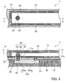
- FIG. 3 illustrates an electronic apparatus according to an embodiment.
- A) of FIG. 3 is a schematic plan view of a main portion of an electronic apparatus according to an embodiment.
- (B) of FIG. 3 is a schematic sectional view of the main portion of the electronic apparatus according to the embodiment.
- A) of FIG. 3 is a schematic plan view taken along line P2-P2 in (B) of FIG. 3 .
- (B) of FIG. 3 is a schematic sectional view taken along line P1-P1 in (A) of FIG. 3 .
- An electronic apparatus 1 illustrated in (A) and (B) of FIG. 3 includes a substrate 20 and a waveguide 10.
- the waveguide 10 includes a lower conductor 11, an upper conductor 12, and a sidewall conductor 13.
- the upper conductor 12 is formed opposite the lower conductor 11, and the lower conductor 11 and the upper conductor 12 are connected by the sidewall conductor 13.
- the inside of the waveguide 10 is hollow.
- An insulating layer 30 is formed on the outside of the waveguide 10.
- FIG. 3 illustrates a pseudo SoC (System on Chip) substrate as an example of the substrate 20.
- the substrate 20 may be a wafer that has not been divided yet into chips by dicing or may be a chip obtained by dividing a wafer by dicing.
- the substrate 20 includes a resin layer 21 and a semiconductor chip 22 embedded in the resin layer 21.
- the semiconductor chip 22 has a plurality of terminals 22a.
- FIG. 3 illustrates a ground (GND) terminal 22aa and a signal terminal 22ab as examples of the terminals 22a.
- the semiconductor chip 22 is embedded in the resin layer 21 in such a manner that the GND terminal 22aa and the signal terminal 22ab (the terminals 22a) are exposed on a surface 21a of the resin layer 21.
- the waveguide 10 is formed on such a pseudo SoC substrate that includes the resin layer 21 and the semiconductor chip 22 as the substrate 20, the waveguide 10 may alternatively be formed on a semiconductor chip, an interposer, a circuit board, or the like.
- the pseudo SoC substrate as illustrated in (B) of FIG. 3 is used as an example of the substrate 20.
- the lower conductor 11 of the waveguide 10 is formed above the substrate 20 via the insulating layer 30 and is electrically connected to the GND terminal 22aa of the semiconductor chip 22 in the substrate 20.
- the lower conductor 11 has an opening 11a at a position corresponding to the signal terminal 22ab of the semiconductor chip 22.
- a conductor pin (a columnar conductor) 40 is formed on the signal terminal 22ab corresponding to the opening 11a.
- the conductor pin 40 extends from the signal terminal 22ab to the upper conductor 12 through the opening 11a of the lower conductor 11. The top end of the conductor pin 40 reaches the upper conductor 12.
- the conductor pin 40 includes a lower-layer pin 41 formed on the signal terminal 22ab, a middle-layer pin 42 formed on the pin 41, and an upper-layer pin 43 formed on the pin 42 and connected (short-circuited) to the upper conductor 12.
- the pin 41 is formed with a height from the signal terminal 22ab to the top surface of the lower conductor 11 (of the opening 11a), and the pins 42 and 43 are each formed with a height half of the height from the top surface of the lower conductor 11 to the bottom surface of the upper conductor 12.
- the diameter (the cross-sectional width in the planar direction) of each of the pins 41 to 43 of the conductor pin 40 may be set to a desired value.
- the diameter of the pin 42 is larger than that of the pin 41
- the diameter of the pin 43 is smaller than that of the pin 42.
- Each of the pins 41 to 43 of the conductor pin 40 may have an arbitrary cross-sectional shape in the planar direction.
- the cross-sectional shape may be nearly circular, elliptical, nearly elliptical, rectangular, or nearly rectangular.
- the number of pins 41 to 43 of the conductor pin 40 connect the signal terminal 22ab of the semiconductor chip 22 with the upper conductor 12 of the waveguide 10, the number of pins is not limited to three.
- the number of pin layers may be set to one or more. In the example in FIG. 3 , for convenience of description, the number of pin layers of the conductor pin 40 is set to three.
- signal transmission is performed between the waveguide 10 and the substrate 20 (the signal terminal 22ab of the semiconductor chip 22).
- the distance from the lower conductor 11 to the upper conductor 12 of the waveguide 10, namely, the thickness (height) of the waveguide 10 is equal to or less than one fourth of the wavelength of a signal transmitted between the semiconductor chip 22 and the waveguide 10.
- the impedance of the semiconductor chip 22 and the impedance of the waveguide 10 are adjusted (matched) by changing the diameters of the pins 41 to 43 of the conductor pin 40.
- FIGS. 4 and 5 illustrate analysis examples of transmission characteristics of electronic apparatuses.
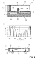
- FIG. 4 illustrates an analysis example of an electronic apparatus 1a (an electronic apparatus in which the waveguide 100 in FIG. 1 is formed).
- a conductor pin 40a formed on a signal terminal 22ab of a semiconductor chip 22 is not connected (short-circuited) to an upper conductor 12 of a waveguide 10.
- A) of FIG. 4 is a schematic sectional view of a main portion of the electronic apparatus 1a.
- the waveguide 10 has a thickness (the distance between a lower conductor 11 and the upper conductor 12) of 432 ⁇ m.
- B) of FIG. 4 illustrates examples of results of electromagnetic field analysis of the electronic apparatus 1a.
- FIG. 4 illustrates an example of a relationship between the frequency [GHz] and S parameters [dB] obtained from the electromagnetic field analysis.
- the distance between two conductor pins 40a formed on two ports (ports 1 and 2) of the waveguide 10 is set to 3 mm.
- S11 is used for evaluating reflection characteristics
- S21 is used for evaluating transmission characteristics.
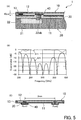
- FIG. 5 illustrates an analysis example of the electronic apparatus 1 in FIG. 3 .
- the conductor pin 40 formed on the signal terminal 22ab of the semiconductor chip 22 is connected (short-circuited) to the upper conductor 12 of the waveguide 10.
- (A) of FIG. 5 is a schematic sectional view of a main portion of the electronic apparatus 1.
- the waveguide 10 has a thickness (the distance between the lower conductor 11 and the upper conductor 12) of 40 ⁇ m.
- B) of FIG. 5 illustrates examples of results of electromagnetic field analysis of the electronic apparatus 1.
- (B) of FIG. 5 illustrates an example of a relationship between the frequency [GHz] and S parameters [dB] obtained from the electromagnetic field analysis.
- the distance between two conductor pins 40 formed on two ports (ports 1 and 2) of the waveguide 10 is set to 3 mm.
- S11 is used for evaluating reflection characteristics of a transmission signal
- S21 is used for evaluating transmission characteristics of the transmission signal.
- Each S parameter (S11 and S21) in (B) of FIG. 4 and (B) of FIG. 5 is calculated in dB as the logarithm of an absolute value
- the logarithm of an absolute value
- the thickness of the waveguide 10 in the electronic apparatus 1 ((A) of FIG. 5 ) in which the conductor pin 40 on the signal terminal 22ab is short-circuited to the waveguide 10 is approximately one tenth of that of the waveguide 10 in the electronic apparatus 1a ((A) of FIG. 4 ) in which the conductor pin 40a is not short-circuited to the waveguide 10.
- (B) of FIG. 4 and (B) of FIG. 5 indicate that the transmission loss of the electronic apparatus 1 ((A) of FIG. 5 ) in which the conductor pin 40 is short-circuited to the waveguide 10 is equivalent to that of the electronic apparatus 1a ((A) of FIG.
- the electronic apparatus 1 has the waveguide 10 having a thickness approximately one tenth of that of the waveguide 10 of the electronic apparatus 1a while achieving a transmission loss equivalent to that of the electronic apparatus 1a.
- FIGS. 6 and 7 illustrate analysis examples of transmission characteristics of waveguide conversion portions.
- FIG. 6 illustrates models of conversion portions of waveguides 10 having conductor pins in different shapes.
- A of FIG. 6 illustrates Model A that corresponds to the waveguide 100 in FIG. 1 . Namely, in Model A, a conductor pin 40a is not short-circuited to the waveguide 10.
- B and C illustrate models in which a conductor pin 40 is short-circuited to the waveguide 10.
- B of FIG. 6 illustrates Model B in which the conductor pin 40 having a certain diameter is short-circuited to the waveguide 10.
- C of FIG. 6 illustrates Model C in which the conductor pin 40 having components with different diameters is short-circuited to the waveguide 10.
- FIG. 7 illustrates examples of relationships between the frequency and S parameters obtained from electromagnetic field analysis of input and output ports (ports 1 and 2) of the conversion portions of Models A to C illustrated in (A) to (C) of FIG. 6 .
- (A) of FIG. 7 illustrates an example of a relationship between the frequency [GHz] and S11 [dB] per model.
- (B) of FIG. 7 illustrates an example of a relationship between the frequency [GHz] and S21 [dB] per model.
- S11 is used for evaluating reflection characteristics of a transmission signal
- S21 is used for evaluating transmission characteristics of the transmission signal.
- (A) and (B) of FIG. 7 indicate that the values of S11 of the Models B and C, in which the conductor pin 40 is short-circuited to the waveguide 10, are lower than that of the Model A, in which the conductor pin 40a is not short-circuited to the waveguide 10, and the values of S21 of the Models B and C are higher than that of the Model A.
- S11 is an index of the reflection characteristics of a transmission signal
- S21 is an index of the transmission characteristics. Namely, the conversion portions of the waveguides 10 of Models B and C represent smaller transmission loss, compared to Model A.
- the shape of the conductor pin 40 short-circuited to the waveguide 10 affects the reflection characteristics and the transmission characteristics of a transmission signal.
- the reflection characteristics and the transmission characteristics at the conversion portion of the waveguide 10 can be adjusted.
- the impedance matching between the waveguide 10 and the signal line can also be performed.
- FIGS. 8 to 12 illustrate a conductor pin designing method according to an embodiment.
- FIG. 8 schematically illustrates the electronic apparatus including the conductor pin and the waveguide at an initial design stage.
- A) of FIG. 8 is a schematic plan view of a main portion of the electronic apparatus.
- B) of FIG. 8 is a schematic sectional view of the main portion of the electronic apparatus.
- a diameter Dp of the pin 41 which is formed on the signal terminal 22ab of the semiconductor chip 22, is set to a certain value.
- the diameter Dp of the pin 41 is set on the basis of the size of the signal terminal 22ab in the planar direction.
- the pins 42 and 43 formed on the pin 41 are also formed to have the diameter Dp.
- the opening 11a formed in the lower conductor 11 of the waveguide 10 may be formed to have a size (diameter) Dh so that the characteristic impedance represents a predetermined value, for example, 50 ⁇ , when the pin 41, the insulating layer 30, and the lower conductor 11 are deemed to be a coaxial line having the pin 41 as its center conductor.
- the thickness b and the width a of the waveguide 10 may be set to certain values, respectively. However, it is desirable that the thickness b and the width a be set on the basis of the frequency of a signal transmitted.
- the distance (a back stub length Lb) from the sidewall conductor 13 to the conductor pin 40 may be set to approximately one fourth of the wavelength of a signal transmitted in the waveguide 10, for example.
- the waveguide 10 allows a signal having a frequency of 300 GHz to transmit
- the diameter Dp of the conductor pin 40 (the pin 41) connected to the waveguide 10 is 100 ⁇ m
- the diameter Dh of the opening of the lower conductor 11 is 230 ⁇ m.
- the width a, the thickness b, and the back stub length Lb of the waveguide 10 are 864 ⁇ m, 40 ⁇ m, and 300 ⁇ m, respectively.
- the diameters of the pins 42 and 43 on the pin 41 are adjusted. However, in this adjustment, the lengths of the pins 41 to 43 are not changed.
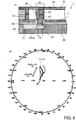
- FIG. 9 illustrates a first adjustment made to the conductor pin.
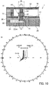
- A) of FIG. 9 is a schematic sectional view of a main portion of an example of the electronic apparatus at a first adjustment stage.
- B) of FIG. 9 illustrates an example of a Smith chart at the first adjustment stage.
- the Smith chart in (B) of FIG. 9 indicates the input impedance (normalized) seen from the semiconductor chip 22.
- the impedance matching cannot be achieved by adjusting the diameter Db of the pins 42 and 43, the diameter of the upper pin 43 alone is further adjusted. However, in this adjustment, the lengths of the pins 41 to 43 are not changed.
- FIG. 10 illustrates a second adjustment made to the conductor pin.
- A) of FIG. 10 is a schematic sectional view of the main portion of the example of the electronic apparatus at a second adjustment stage.
- B) of FIG. 10 illustrates an example of a Smith chart at the second adjustment stage.
- the Smith chart in (B) of FIG. 10 indicates the input impedance (normalized) seen from the semiconductor chip 22.
- the resistance value of the conductor pin 40 is decreased. As a result, the real part of the input impedance is decreased. In addition, the capacitance between the pin 43 and the lower conductor 11 is increased, and the imaginary part of the input impedance is also changed to some extent.
- FIGS. 11 and 12 illustrate an example of impedance matching.
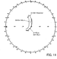
- FIG. 11 is a Smith chart illustrating an example in which impedance matching is achieved by performing the first adjustment described with FIG. 9 first and the second adjustment described with FIG. 10 next.
- FIG. 12 illustrates examples of relationships between the frequency [GHz] and S parameters [dB]. These relationships have been obtained by conducting electromagnetic field analysis before any of the adjustments is performed, after the first adjustment is performed, and after the second adjustment is performed.
- S11 is used for evaluating reflection characteristics of a transmission signal
- S21 is used for evaluating transmission characteristics of the transmission signal.
- the diameter Db of the pin 43 and the pin 42 on the pin 41 of the conductor pin 40 is adjusted so that the imaginary part of the input impedance reaches 0 or nearly 0 at around the frequency of a transmission signal.
- the diameter Dt of the upper pin 43 of the conductor pin 40 is adjusted so that the real part of the input impedance reaches 1 or nearly 1.
- the resistance value of the conductor pin 40 is increased.
- the real part of the input impedance increases and reaches 1 or nearly 1. Namely, the impedance matching is achieved.
- a fine diameter adjustment may be made to at least one of the pins 41 to 43 of the conductor pin 40 so that even better impedance matching can be achieved.
- the first adjustment is made to the unadjusted conductor pin 40.
- the second adjustment is made to the adjusted conductor pin 40.
- S11 which is as an index of the reflection characteristics of a transmission signal
- S21 which is an index of the transmission characteristics.
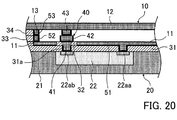
- FIGS. 13 to 20 is a schematic sectional view of a main portion of an electronic apparatus at each step in the forming method.
- a substrate 20 (a pseudo SoC substrate) including a resin layer 21 and a semiconductor chip 22 embedded therein is prepared.
- epoxy resin mixed with silica filler or the like is used as the resin layer 21 of the substrate 20.
- the periphery of the semiconductor chip 22 is covered with the resin layer 21 in such a manner that a side on which terminals 22a (22aa and 22ab) are arranged is exposed.
- the resin layer 21 is shaped by heating.
- other semiconductor chips and chip components such as chip capacitors may be embedded in the resin layer 21 of the substrate 20.
- a wafer (a pseudo wafer) that has not been divided yet into chips by dicing is used as the substrate 20.
- a chip obtained by dividing a pseudo wafer by dicing may be used as the substrate 20.
- an insulating layer 31 (a part of the above insulating layer 30) having openings 31a on the terminals 22a of the semiconductor chip 22 embedded in the substrate 20 is formed.
- photosensitive phenol resin is applied with a thickness of 10 ⁇ m onto the substrate 20.
- the photosensitive phenol resin is developed with tetramethylammonium hydroxide (TMAH) or the like.
- TMAH tetramethylammonium hydroxide
- the photosensitive phenol resin is cured at a temperature between 200°C and 250°C, for example, at 200°C.
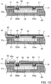
- the insulating layer 31 having the openings 31a as illustrated in (B) of FIG. 13 is formed.
- a seed layer 51 is formed on the insulating layer 31 including the openings 31a.
- the seed layer 51 is formed by forming a titanium (Ti) layer having a thickness of 20 nm on the insulating layer 31 by sputtering and by forming a copper (Cu) layer having a thickness of 100 nm on the Ti layer by sputtering.
- a resist pattern 61 having openings 61a is formed on the seed layer 51.
- the openings 61a correspond to areas where the pin 41 of the conductor pin 40 and the lower conductor 11 of the waveguide 10 are to be formed.
- resist material is applied with a thickness of 8 ⁇ m onto the seed layer 51.
- the resist material is developed with TMAH or the like.
- the resist pattern 61 is formed on areas that separate the pin 41 to be formed on the signal terminal 22ab of the semiconductor chip 22 from the lower conductor 11.
- the pin 41 at the bottom layer of the conductor pin 40 and the lower conductor 11 of the waveguide 10 are formed in the openings 61a of the resist pattern 61.
- the pin 41 and the lower conductor 11 are formed by depositing Cu as the conductor material through electrolytic plating in which the seed layer 51 is used as a power feeding layer.
- the lower conductor 11 has a height of 5 ⁇ m.
- the lower conductor 11 is connected to the GND terminal 22aa of the semiconductor chip 22.
- the pin 41 is connected to the signal terminal 22ab of the semiconductor chip 22.
- the resist pattern 61 and a part of the seed layer 51 are removed.
- the resist pattern 61 is removed by using acetone or the like.
- the part of the seed layer 51 exposed as a result of the removal of the resist pattern 61 is removed.
- the Cu layer is selectively removed first, and the Ti layer is selectively removed next.
- the Cu layer is selectively removed by wet etching in which potassium sulfate (K 2 SO 4 ) is used as an etchant.
- the Ti layer is selectively removed by dry etching in which a mixed gas of carbon tetrafluoride (CF 4 ) and oxygen (O 2 ) is used.
- an insulating layer 32 (a part of the above insulating layer 30) is formed on the areas from which the resist pattern 61 and the part of the seed layer 51 have been removed.
- photosensitive phenol resin is applied with a thickness of 5 ⁇ m to the areas.
- the photosensitive phenol resin is developed with TMAH or the like.
- the photosensitive phenol resin is cured at a temperature of 200°C.
- the insulating layer 32 as illustrated in (A) of FIG. 15 is formed.
- an insulating layer 33 (a part of the above insulating layer 30) is formed on an area to be the outside of the waveguide 10 being formed.
- photosensitive phenol resin is applied with a thickness of 10 ⁇ m to the area.
- the photosensitive phenol resin is developed with TMAH or the like.
- the photosensitive phenol resin is cured at a temperature of 200°C.
- the insulating layer 33 as illustrated in (B) of FIG. 15 is formed.
- a sacrificial layer 62 having openings 62a is formed.
- the openings 62a correspond to areas where the pin 42 of the conductor pin 40 and the sidewall conductor 13 of the waveguide 10 are to be formed.
- resist material is applied with a thickness of 10 ⁇ m.
- the resist material is developed with TMAH or the like.
- the diameter of the opening 62a that corresponds to the area where the pin 42 is to be formed is set based on the diameter of the pin 42 to be formed.
- the opening 62a is formed to have a diameter larger than that of the pin 41 formed on the signal terminal 22ab.
- a seed layer 52 is formed on the sacrificial layer 62 including the openings 62a.
- the seed layer 52 is formed by forming a Ti layer and a Cu layer having respective predetermined thicknesses by sputtering.
- a resist pattern 63 having openings 63a is formed on the seed layer 52.
- the openings 63a correspond to areas where the pin 42 of the conductor pin 40 and the sidewall conductor 13 of the waveguide 10 are to be formed.
- resist material is applied with a thickness of 8 ⁇ m onto the seed layer 52.
- the resist material is developed with TMAH or the like.
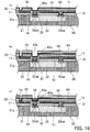
- the pin 42 (the middle layer) of the conductor pin 40 and the sidewall conductor 13 (the lower layer) of the waveguide 10 are formed in the openings 62a of the sacrificial layer 62 located at the openings 63a of the resist pattern 63.
- the pin 42 and the sidewall conductor 13 are formed by depositing Cu through electrolytic plating in which the seed layer 52 is used as a power feeding layer.
- the pin 42 and the sidewall conductor 13 formed in this step have a height of 10 ⁇ m.
- the resist pattern 63 and a part of the seed layer 52 are removed.
- the resist pattern 63 is removed by using acetone or the like.
- the part of the seed layer 52 exposed as a result of the removal of the resist pattern 63 is selectively removed by etching. By removing the seed layer 52, the pin 42 and the sidewall conductor 13 are electrically separated.
- an insulating layer 34 (a part of the above insulating layer 30) is formed on an area to be the outside of the waveguide 10 being formed.
- photosensitive phenol resin is applied with a thickness of 10 ⁇ m.
- the photosensitive phenol resin is developed with TMAH or the like.
- the photosensitive phenol resin is cured at a temperature of 200°C. As a result, the insulating layer 34 is formed.
- a sacrificial layer 64 having openings 64a is formed.
- the openings 64a correspond to areas where the pin 43 of the conductor pin 40 and the sidewall conductor 13 of the waveguide 10 are to be formed.
- resist material is applied with a thickness of 10 ⁇ m.
- the resist material is developed with TMAH or the like.
- the diameter of the opening 64a that corresponds to the area where the pin 43 is to be formed is set based on the diameter of the pin 43. In the example in (C) of FIG. 17 , the diameter of the opening 64a is smaller than that of the pin 42 formed earlier.
- a seed layer 53 is formed on the sacrificial layer 64 including the openings 64a.
- the seed layer 53 is formed by forming a Ti layer and a Cu layer having respective predetermined thicknesses by sputtering.
- a resist pattern 65 having openings 65a is formed on the seed layer 53.
- the openings 65a correspond to areas where the pin 43 of the conductor pin 40 and the sidewall conductor 13 of the waveguide 10 are to be formed.
- resist material is applied with a thickness of 8 ⁇ m onto the seed layer 53.
- the resist material is developed with TMAH or the like.
- the pin 43 (the upper layer) of the conductor pin 40 and the sidewall conductor 13 (the upper layer) of the waveguide 10 are formed in the openings 64a of the sacrificial layer 64 located at the openings 65a of the resist pattern 65.
- the pin 43 and the sidewall conductor 13 are formed by depositing Cu through electrolytic plating in which the seed layer 53 is used as a power feeding layer.
- the pin 43 and the sidewall conductor 13 formed in this step have a height of 10 ⁇ m.
- the resist pattern 65 is removed, and the seed layer 53 exposed as a result of the removal of the resist pattern 65 is removed.
- the resist pattern 65 is removed by using acetone or the like, and the seed layer 53 is selectively removed by etching. By removing the seed layer 53, the pin 43 and the sidewall conductor 13 are electrically separated.
- the sacrificial layers 62 and 64 are removed.
- the sacrificial layers 62 and 64 are removed by using acetone or the like. By removing the sacrificial layers 62 and 64, the hollow portion of the waveguide 10 is formed.
- the upper conductor 12 of the waveguide 10 is formed.
- metal foil made of Cu or the like is adhered on the insulating layer 34, the sidewall conductor 13, and the conductor pin 40 by lamination.
- the metal foil has a thickness of 20 ⁇ m.
- a pseudo wafer that has not been divided into chips is used as the substrate 20
- a pseudo wafer in which the resin layer 21 including the semiconductor chips 22 and the waveguides 10 are integrated is obtained.
- an individual electronic apparatus 1 including a waveguide 10 is obtained.
- the conductor pin 40 having three layers of the pins 41 to 43 has been formed as an example.
- the conductor pin 40 with four or more pin layers may be formed by repeating the steps from (B) of FIG. 17 to (A) of FIG. 19 as many times as needed by the number of pin layers after the step in (A) of FIG. 19 and performing the steps subsequent to the step in (B) of FIG. 19 .
- the conductor pin 40 with two pin layers may also be formed by omitting the steps from (B) of FIG. 17 to (A) of FIG. 19 after performing the step in (A) of FIG. 17 , removing the sacrificial layer 62 in accordance with the example in (B) of FIG. 19 , and forming the upper conductor 12 in accordance with the example in (C) of FIG. 19 .
- the waveguide 10 described above may be configured to have an antenna function.
- FIG. 21 illustrates an electronic apparatus as a variation.
- FIG. 21 is a schematic sectional view of a main portion of an electronic apparatus as a variation.
- An electronic apparatus 1A illustrated in FIG. 21 differs from the electronic apparatus 1 illustrated, for example, in FIG. 3 in that at least one slot 12a is formed in an upper conductor 12 of a waveguide 10. While the upper conductor 12 has one slot 12a in the example in FIG. 21 , the upper conductor 12 may have a plurality of slots 12a. In addition, for example, the shape and the position of an individual slot 12a and the alignment (the slot pattern) of a plurality of slots 12a may be set as appropriate on the basis of various characteristics such as the frequency of a transmitted or received signal.
- the waveguide 10 is allowed to have an antenna function, in addition to the signal transmission function.
- the electronic apparatus 1A has a thin waveguide 10 performing signal transmission and reception, having a conversion portion in which a conductor pin 40 is short-circuited to the upper conductor 12, and enabling low transmission loss at the conversion portion.
- the electronic apparatus 1A is formed in accordance with the example described with FIGS. 13 to 19 as the method for forming the electronic apparatus 1.
- the upper conductor 12 that is made of metal foil or the like and that has the slot 12a formed in advance is adhered on an insulating layer 30 (34), a sidewall conductor 13, and the conductor pin 40 by lamination.
- the electronic apparatus 1A may be formed by using the following method.
- the electronic apparatus 1A is formed by performing the same steps as those in the method for forming the electronic apparatus 1 until the step for forming the seed layer 53 described with (A) of FIG. 18 .
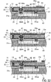
- the subsequent steps will be described with reference to FIGS. 22 and 23 .
- a resist pattern 65 having an opening 65a is formed as illustrated in (A) of FIG. 22 .
- the opening 65a corresponds to an area where a pin 43 of the conductor pin 40 and the sidewall conductor 13 and the upper conductor 12 of the waveguide 10 are to be formed.
- the upper conductor 12 that has the pin 43 (the upper layer) of the conductor pin 40, the sidewall conductor 13 (the upper layer) of the waveguide 10, and the slot 12a is formed in the opening 65a of the resist pattern 65.
- the pin 43, the sidewall conductor 13, and the upper conductor 12 are formed by depositing conductor material such as Cu through electrolytic plating in which the seed layer 53 is used as a power feeding layer.
- the resist pattern 65 is removed, and the seed layer 53 exposed as a result of the removal of the resist pattern 65 is removed.
- the sacrificial layers 62 and 64 are removed by using an etchant such as acetone. In this way, the waveguide 10 having a hollow portion as illustrated in FIG. 23 is formed.
- the etchant flows into and out of the waveguide 10 through the slot 12a of the upper conductor 12. In this way, the sacrificial layers 62 and 64 are etched and removed from the inside of the waveguide 10.
- the electronic apparatus 1A including the waveguide 10 having the slot 12a is formed.
- the resist pattern 65 is used as a mask and the upper conductor 12 is formed by using plating, slot patterns in various shapes, arrangements, and sizes can accurately be formed.
- the steps in (A) to (C) of FIG. 22 and FIG. 23 are performed.
- the pin 43 and the sidewall conductor 13 are formed by performing the step in (A) of FIG. 19
- the upper conductor 12 having the slot 12a may be formed in accordance with the procedure in (A) to (C) of FIG. 22 and FIG. 23 .
- the top end of the conductor pin 40 vertically arranged on a signal terminal 22ab of a semiconductor chip 22 is connected and short-circuited to the upper conductor 12 of the waveguide 10 having a lower conductor 11, the sidewall conductor 13, and the upper conductor 12.
- the diameter of the conductor pin 40 is adjusted so that the impedance matching is achieved between the semiconductor chip 22 and the waveguide 10.
- This waveguide 10 enables low-loss signal transmission between the semiconductor chip 22 and the waveguide 10 even when the signal transmitted is a high-frequency signal over a millimeter-wave signal.
- the waveguide 10 can be formed by using a rewiring technique.
- the waveguide 10 can be formed to have a wider width than a wiring formed in a semiconductor process and have a thickness as thin as an insulating portion (an insulating layer) of a rewiring layer formed by the rewiring technique.
- the thin electronic apparatus 1 or 1A that achieves low transmission loss is realized.
- the rewiring technique used for integrating heterogeneous devices including a pseudo SoC as described above is effective in reducing the transmission loss in a transmission line that connects elements. This is because the rewiring technique can make the length of a transmission line between elements relatively short and the width of the transmission line relatively wider than a transmission line formed in a semiconductor process.
- various problems occur in a frequency range higher than the millimeter-wave band. For example, the transmission line length becomes non-negligible with respect to the wavelength, the conductor loss due to the skin effect is increased, and the dielectric loss of insulating material becomes non-negligible.
- the waveguide 10 that is wide, thin, and hollow is realized by using the rewiring technique.
- the diameter of the conductor pin 40 short-circuited to the waveguide 10 low-loss signal transmission is realized.
- the waveguide 10 may be formed to have a width of 500 ⁇ m or more, a thickness of around 40 ⁇ m, and transmission characteristics of -0.5 dB.
- the waveguide 10 may be provided with a dielectric material therein.
- the waveguide 10 (or the waveguide 10 having an antenna function) may be formed on a semiconductor chip alone or on a circuit board such as a printed circuit board or an interposer.
- FIG. 24 illustrates, as variations, electronic apparatuses, each of which includes a waveguide formed on a semiconductor chip.
- A) of FIG. 24 is a schematic sectional view of a first configuration example of a main portion of an electronic apparatus including a waveguide formed on a semiconductor chip.
- B) of FIG. 24 is a schematic sectional view of a second configuration example of a main portion of an electronic apparatus including a waveguide formed on a semiconductor chip.
- An electronic apparatus 1B illustrated in (A) of FIG. 24 includes a semiconductor chip 70 and a waveguide 10 formed on the semiconductor chip 70.
- the semiconductor chip 70 includes a semiconductor substrate 71 made of silicon (Si), etc. and a wiring layer 72 formed on the semiconductor substrate 71.
- Circuit elements (not illustrated) such as transistors, resistors, and capacitors are formed on the front surface (the side on which the wiring layer 72 is arranged) of the semiconductor substrate 71.
- the wiring layer 72 includes conductor portions (not illustrated) such as vias and wirings that are electrically connected to circuit elements such as transistors formed on the semiconductor substrate 71.
- the wiring layer 72 also includes an insulating portion (not illustrated) formed around the conductor portion.
- a GND terminal 22aa and a signal terminal 22ab are arranged in the conductor portion at the top layer of the wiring layer 72.
- the waveguide 10 is formed on the wiring layer 72 of this semiconductor chip 70.
- a conductor pin 40 formed on the signal terminal 22ab is connected to an upper conductor 12 of the waveguide 10.
- a lower conductor 11 of the waveguide 10 is connected to the GND terminal 22aa.
- an electronic apparatus 1C illustrated in (B) of FIG. 24 includes a semiconductor chip 70 and a waveguide 10 formed on the semiconductor chip 70.
- through-electrodes 73 that penetrate a semiconductor substrate 71 and are electrically connected to a wiring layer 72 formed on the front surface (the side on which circuit elements such as transistors, etc. are formed) of the semiconductor substrate 71 are formed on the semiconductor chip 70 by using a TSV (Through Silicon Via) technique or the like.
- a GND terminal 22aa and a signal terminal 22ab are arranged on the sides of the through-electrodes 73, the sides being opposite to the side on which the wiring layer 72 is arranged.
- a conductor pin 40 formed on the signal terminal 22ab is connected to an upper conductor 12 of the waveguide 10.
- the lower conductor 11 of the waveguide 10 is connected to the GND terminal 22aa.
- the waveguide 10 can be formed on the semiconductor chip 70.
- the waveguide 10 can be formed on the side on which the wiring layer 72 is arranged or on the back side of the semiconductor substrate 71 (the opposite side of the side on which the wiring layer 72 is arranged).
- a slot (the slot 12a, for example) may be formed in the upper conductor 12 of each of the waveguides 10 to provide the electronic apparatuses 1B and 1C with an antenna function.
- FIG. 25 illustrates, as a variation, an electronic apparatus including a waveguide formed on a circuit board.
- FIG. 25 is a schematic sectional view of a configuration example of a main portion of an electronic apparatus including a waveguide formed on a circuit board.
- An electronic apparatus 1D illustrated in FIG. 25 includes a circuit board 80 and a waveguide 10 formed on the circuit board 80.
- the circuit board 80 includes a substrate 81 and conductor portions 82 (wirings, vias, etc.) arranged, for example, inside and on the front surface of the substrate 81.
- FIG. 25 illustrates the circuit board 80 in which the front and back sides (both of the main sides) are electrically connected with each other by the conductor portions 82.
- the circuit board 80 is an interposer or a printed circuit board in which insulating material such as resin is used as the substrate 81.
- the circuit board 80 may be an Si interposer in which an Si semiconductor substrate is used as at least a part of the substrate 81.
- a GND terminal 22aa and a signal terminal 22ab are arranged on the conductor portions 82 exposed on one side of the circuit board 80.
- the waveguide 10 is formed on this circuit board 80.
- a conductor pin 40 formed on the signal terminal 22ab is connected to an upper conductor 12 of the waveguide 10.
- a lower conductor 11 of the waveguide 10 is connected to the GND terminal 22aa.
- the waveguide 10 can be formed on the circuit board 80.
- a slot (the slot 12a, for example) can be formed in the upper conductor 12 of the waveguide 10 to provide the electronic apparatuses 1D with an antenna function.
Landscapes
- Engineering & Computer Science (AREA)
- Manufacturing & Machinery (AREA)
- Waveguides (AREA)
- Waveguide Aerials (AREA)
Abstract
Description
- The embodiments discussed herein relate to an electronic apparatus and a manufacturing method thereof.
- Waveguides have conventionally been used for signal transmission in electronic devices. For example, there has been proposed a semiconductor device including a semiconductor chip and a waveguide that is formed thereabove or therebelow. This waveguide includes a transmitting antenna and a receiving antenna that are electrically connected to the semiconductor chip and that are not in contact with the waveguide.
- PTL1: Japanese Laid-open Patent Publication No.
2008-148041 - Waveguides enable signal transmission with lower loss than planar transmission lines. However, these waveguides having conventional structures are large in size. Namely, it is difficult to manufacture small electronic devices including waveguides.
- According to one aspect, there is provided an electronic apparatus including: a substrate which includes a terminal; a waveguide which includes a lower conductor that is formed above the substrate and that has an opening at a position corresponding to the terminal and which includes an upper conductor that is arranged above the lower conductor; and a columnar conductor which is formed above the terminal, which penetrates the opening without contacting the lower conductor, and which is connected to the upper conductor.
- According to another aspect, there is provided an electronic apparatus manufacturing method including: preparing a substrate having a terminal; and forming, above the substrate, a waveguide which includes a lower conductor that has an opening at a position corresponding to the terminal and which includes an upper conductor arranged above the lower conductor, wherein the forming of the waveguide includes forming, above the terminal, a columnar conductor which penetrates the opening without contacting the lower conductor and which is connected to the upper conductor.
- According to the embodiments discussed herein, a small electronic apparatus including a waveguide that enables low-loss signal transmission is formed.
- The objects, features and advantages of the present technique will be apparent from the accompanying drawings representing suitable embodiments as examples of the present technique and from the following related description.
-
- [
FIG. 1] FIG. 1 illustrates a waveguide as one mode. - [
FIG. 2] FIG. 2 illustrates a waveguide as another mode. - [
FIG. 3] FIG. 3 illustrates an electronic apparatus according to an embodiment. - [
FIG. 4] FIG. 4 illustrates an analysis example of transmission characteristics of an electronic apparatus (part 1). - [
FIG. 5] FIG. 5 illustrates an analysis example of transmission characteristics of an electronic apparatus (part 2). - [
FIG. 6] FIG. 6 illustrates analysis examples of transmission characteristics of waveguide conversion portions (part 1). - [
FIG. 7] FIG. 7 illustrates analysis examples of transmission characteristics of waveguide conversion portions (part 2). - [
FIG. 8] FIG. 8 illustrates a conductor pin designing method according to an embodiment (part 1). - [
FIG. 9] FIG. 9 illustrates the conductor pin designing method according to the embodiment (part 2). - [
FIG. 10] FIG. 10 illustrates the conductor pin designing method according to the embodiment (part 3). - [
FIG. 11] FIG. 11 illustrates the conductor pin designing method according to the embodiment (part 4). - [
FIG. 12] FIG. 12 illustrates the conductor pin designing method according to the embodiment (part 5). - [
FIG. 13] FIG. 13 illustrates a forming method of an electronic apparatus including a waveguide according to the embodiment (part 1). - [
FIG. 14] FIG. 14 illustrates the forming method of an electronic apparatus including a waveguide according to the embodiment (part 2). - [
FIG. 15] FIG. 15 illustrates the forming method of an electronic apparatus including a waveguide according to the embodiment (part 3). - [
FIG. 16] FIG. 16 illustrates the forming method of an electronic apparatus including a waveguide according to the embodiment (part 4). - [
FIG. 17] FIG. 17 illustrates the forming method of an electronic apparatus including a waveguide according to the embodiment (part 5). - [
FIG. 18] FIG. 18 illustrates the forming method of an electronic apparatus including a waveguide according to the embodiment (part 6). - [
FIG. 19] FIG. 19 illustrates the forming method of an electronic apparatus including a waveguide according to the embodiment (part 7). - [
FIG. 20] FIG. 20 illustrates the forming method of an electronic apparatus including a waveguide according to the embodiment (part 8). - [
FIG. 21] FIG. 21 illustrates an electronic apparatus as a variation. - [
FIG. 22] FIG. 22 illustrates, as a variation, a forming method of an electronic apparatus including a waveguide (part 1). - [
FIG. 23] FIG. 23 illustrates, as a variation, the forming method of an electronic apparatus including a waveguide (part 2). - [
FIG. 24] FIG. 24 illustrates, as variations, electronic apparatuses, each of which includes a waveguide formed on a semiconductor chip. - [
FIG. 25] FIG. 25 illustrates, as a variation, an electronic apparatus including a waveguide formed on a circuit board. - First, a waveguide as one mode will be described.
-
FIG. 1 illustrates a waveguide as one mode. (A) ofFIG. 1 is a schematic perspective view of a main portion of a waveguide as one mode. (B) ofFIG. 1 is a schematic sectional view taken along a plane X in (A) ofFIG. 1 . - A
waveguide 100 illustrated in (A) and (B) ofFIG. 1 includes alower conductor 110, anupper conductor 120, and asidewall conductor 130. Theupper conductor 120 is formed opposite thelower conductor 110, and thelower conductor 110 and theupper conductor 120 are connected by thesidewall conductor 130. For example, the inside of thewaveguide 100 is hollow. - The
waveguide 100 is mounted on a device (an electronic apparatus) such as a semiconductor chip or a semiconductor device including a semiconductor chip and is connected to a signal line extended from the device. For example, thewaveguide 100 is connected to a signal line (a coaxial signal line) 200 having a coaxial structure as illustrated in (A) and (B) ofFIG. 1 . - The
coaxial signal line 200 includes acenter conductor 210, aninsulating material 220 formed around thecenter conductor 210, and a coatedconductor 230 formed around theinsulating material 220. By connecting thiscoaxial signal line 200 to thewaveguide 100, signal transmission (mode conversion) is performed between thecoaxial signal line 200 and thewaveguide 100. To convert a signal transmitted, thecoaxial signal line 200 is connected to thewaveguide 100 in such a manner that a portion of thecenter conductor 210 is exposed inside thewaveguide 100 without contacting thewaveguide 100. For example, the portion of thecenter conductor 210 exposed inside thewaveguide 100 has a length I approximately one fourth of the wavelength of a transmission signal. - The
waveguide 100 has a width a set on the basis of the frequency of the transmission signal. In many cases, thewaveguide 100 has a thickness approximately half of the width a as a standard setting. - The
hollow waveguide 100 enables transmission of a high-frequency signal over a millimeter-wave signal with low loss. - However, as in the
waveguide 100, when thecenter conductor 210 of thecoaxial signal line 200 has a portion exposed inside thewaveguide 100 for the length of approximately one fourth of the wavelength of the transmission signal, the size (thickness) of thewaveguide 100 is increased. Consequently, a module including thewaveguide 100 could be increased in size. -
FIG. 2 illustrates a waveguide as another mode. (A) ofFIG. 2 is a schematic perspective view of a main portion of a waveguide as another mode. (B) ofFIG. 2 is a schematic sectional view taken along a plane Y in (A) ofFIG. 2 . - (A) and (B) of
FIG. 2 illustrate an example of awaveguide 100a that is thinner than thewaveguide 100 illustrated in (A) and (B) ofFIG. 1 . Compared with thewaveguide 100, thewaveguide 100a has a smaller thickness between alower conductor 110 and anupper conductor 120. In addition, while acenter conductor 210 of acoaxial signal line 200 has a portion exposed inside thewaveguide 100a, this portion has a smaller length I. - It is possible to manufacture a smaller module by using this
thin waveguide 100a. However, as a result of reducing the thickness, if the length I of the portion of thecenter conductor 210 exposed inside thewaveguide 100a falls short of one fourth of the wavelength of a transmission signal, sufficient impedance matching is not achieved. As a result, good signal transmission may not be performed between thecoaxial signal line 200 and thewaveguide 100a. - In view of the above points, a waveguide that enables low-loss signal transmission and achieves downsizing of a module will hereinafter be described. In addition, an electronic apparatus that includes such a waveguide will also be described.
- Next, a waveguide and an electronic apparatus including the waveguide according to an embodiment will be described in detail.
-
FIG. 3 illustrates an electronic apparatus according to an embodiment. (A) ofFIG. 3 is a schematic plan view of a main portion of an electronic apparatus according to an embodiment. (B) ofFIG. 3 is a schematic sectional view of the main portion of the electronic apparatus according to the embodiment. (A) ofFIG. 3 is a schematic plan view taken along line P2-P2 in (B) ofFIG. 3 . (B) ofFIG. 3 is a schematic sectional view taken along line P1-P1 in (A) ofFIG. 3 . - An
electronic apparatus 1 illustrated in (A) and (B) ofFIG. 3 includes asubstrate 20 and awaveguide 10. - The
waveguide 10 includes alower conductor 11, anupper conductor 12, and asidewall conductor 13. Theupper conductor 12 is formed opposite thelower conductor 11, and thelower conductor 11 and theupper conductor 12 are connected by thesidewall conductor 13. The inside of thewaveguide 10 is hollow. An insulatinglayer 30 is formed on the outside of thewaveguide 10. - The
waveguide 10 is formed above thesubstrate 20.FIG. 3 illustrates a pseudo SoC (System on Chip) substrate as an example of thesubstrate 20. Thesubstrate 20 may be a wafer that has not been divided yet into chips by dicing or may be a chip obtained by dividing a wafer by dicing. Thesubstrate 20 includes aresin layer 21 and asemiconductor chip 22 embedded in theresin layer 21. Thesemiconductor chip 22 has a plurality ofterminals 22a.FIG. 3 illustrates a ground (GND) terminal 22aa and a signal terminal 22ab as examples of theterminals 22a. Thesemiconductor chip 22 is embedded in theresin layer 21 in such a manner that the GND terminal 22aa and the signal terminal 22ab (theterminals 22a) are exposed on asurface 21a of theresin layer 21. - In addition to the
semiconductor chip 22, other semiconductor chips and chip components such as chip capacitors may be embedded in theresin layer 21 of thesubstrate 20. - In addition, while the
waveguide 10 is formed on such a pseudo SoC substrate that includes theresin layer 21 and thesemiconductor chip 22 as thesubstrate 20, thewaveguide 10 may alternatively be formed on a semiconductor chip, an interposer, a circuit board, or the like. In this embodiment, for convenience of description, the pseudo SoC substrate as illustrated in (B) ofFIG. 3 is used as an example of thesubstrate 20. - The
lower conductor 11 of thewaveguide 10 is formed above thesubstrate 20 via the insulatinglayer 30 and is electrically connected to the GND terminal 22aa of thesemiconductor chip 22 in thesubstrate 20. Thelower conductor 11 has anopening 11a at a position corresponding to the signal terminal 22ab of thesemiconductor chip 22. A conductor pin (a columnar conductor) 40 is formed on the signal terminal 22ab corresponding to theopening 11a. Theconductor pin 40 extends from the signal terminal 22ab to theupper conductor 12 through theopening 11a of thelower conductor 11. The top end of theconductor pin 40 reaches theupper conductor 12. - The
conductor pin 40 includes a lower-layer pin 41 formed on the signal terminal 22ab, a middle-layer pin 42 formed on thepin 41, and an upper-layer pin 43 formed on thepin 42 and connected (short-circuited) to theupper conductor 12. In the example inFIG. 3 , thepin 41 is formed with a height from the signal terminal 22ab to the top surface of the lower conductor 11 (of theopening 11a), and thepins lower conductor 11 to the bottom surface of theupper conductor 12. The diameter (the cross-sectional width in the planar direction) of each of thepins 41 to 43 of theconductor pin 40 may be set to a desired value. In the example inFIG. 3 , the diameter of thepin 42 is larger than that of thepin 41, and the diameter of thepin 43 is smaller than that of thepin 42. - Each of the
pins 41 to 43 of theconductor pin 40 may have an arbitrary cross-sectional shape in the planar direction. For example, other than a circular shape, the cross-sectional shape may be nearly circular, elliptical, nearly elliptical, rectangular, or nearly rectangular. - In addition, while the three
pins 41 to 43 of theconductor pin 40 connect the signal terminal 22ab of thesemiconductor chip 22 with theupper conductor 12 of thewaveguide 10, the number of pins is not limited to three. The number of pin layers may be set to one or more. In the example inFIG. 3 , for convenience of description, the number of pin layers of theconductor pin 40 is set to three. - In the
electronic apparatus 1, signal transmission (mode conversion) is performed between thewaveguide 10 and the substrate 20 (the signal terminal 22ab of the semiconductor chip 22). For example, the distance from thelower conductor 11 to theupper conductor 12 of thewaveguide 10, namely, the thickness (height) of thewaveguide 10, is equal to or less than one fourth of the wavelength of a signal transmitted between thesemiconductor chip 22 and thewaveguide 10. The impedance of thesemiconductor chip 22 and the impedance of thewaveguide 10 are adjusted (matched) by changing the diameters of thepins 41 to 43 of theconductor pin 40. -
FIGS. 4 and5 illustrate analysis examples of transmission characteristics of electronic apparatuses. -
FIG. 4 illustrates an analysis example of anelectronic apparatus 1a (an electronic apparatus in which thewaveguide 100 inFIG. 1 is formed). In thiselectronic apparatus 1a, aconductor pin 40a formed on a signal terminal 22ab of asemiconductor chip 22 is not connected (short-circuited) to anupper conductor 12 of awaveguide 10. (A) ofFIG. 4 is a schematic sectional view of a main portion of theelectronic apparatus 1a. In theelectronic apparatus 1a illustrated in (A) ofFIG. 4 , thewaveguide 10 has a thickness (the distance between alower conductor 11 and the upper conductor 12) of 432 µm. (B) ofFIG. 4 illustrates examples of results of electromagnetic field analysis of theelectronic apparatus 1a. (B) ofFIG. 4 illustrates an example of a relationship between the frequency [GHz] and S parameters [dB] obtained from the electromagnetic field analysis. In this electromagnetic field analysis, as illustrated in (C) ofFIG. 4 , the distance between twoconductor pins 40a formed on two ports (ports 1 and 2) of thewaveguide 10 is set to 3 mm. S11 is used for evaluating reflection characteristics, and S21 is used for evaluating transmission characteristics. -
FIG. 5 illustrates an analysis example of theelectronic apparatus 1 inFIG. 3 . In thiselectronic apparatus 1, theconductor pin 40 formed on the signal terminal 22ab of thesemiconductor chip 22 is connected (short-circuited) to theupper conductor 12 of thewaveguide 10. (A) ofFIG. 5 is a schematic sectional view of a main portion of theelectronic apparatus 1. In theelectronic apparatus 1 illustrated in (A) ofFIG. 5 , thewaveguide 10 has a thickness (the distance between thelower conductor 11 and the upper conductor 12) of 40 µm. (B) ofFIG. 5 illustrates examples of results of electromagnetic field analysis of theelectronic apparatus 1. (B) ofFIG. 5 illustrates an example of a relationship between the frequency [GHz] and S parameters [dB] obtained from the electromagnetic field analysis. In this electromagnetic field analysis, as illustrated in (C) ofFIG. 5 , the distance between two conductor pins 40 formed on two ports (ports 1 and 2) of thewaveguide 10 is set to 3 mm. S11 is used for evaluating reflection characteristics of a transmission signal, and S21 is used for evaluating transmission characteristics of the transmission signal. - Each S parameter (S11 and S21) in (B) of
FIG. 4 and (B) ofFIG. 5 is calculated in dB as the logarithm of an absolute value |S|. The same applies to (A) ofFIG. 7 , (B) ofFIG. 7 , andFIG. 12 . - As described above, the thickness of the
waveguide 10 in the electronic apparatus 1 ((A) ofFIG. 5 ) in which theconductor pin 40 on the signal terminal 22ab is short-circuited to thewaveguide 10 is approximately one tenth of that of thewaveguide 10 in theelectronic apparatus 1a ((A) ofFIG. 4 ) in which theconductor pin 40a is not short-circuited to thewaveguide 10. (B) ofFIG. 4 and (B) ofFIG. 5 indicate that the transmission loss of the electronic apparatus 1 ((A) ofFIG. 5 ) in which theconductor pin 40 is short-circuited to thewaveguide 10 is equivalent to that of theelectronic apparatus 1a ((A) ofFIG. 4 ) in which theconductor pin 40a is not short-circuited to thewaveguide 10. Namely, theelectronic apparatus 1 has thewaveguide 10 having a thickness approximately one tenth of that of thewaveguide 10 of theelectronic apparatus 1a while achieving a transmission loss equivalent to that of theelectronic apparatus 1a. -
FIGS. 6 and7 illustrate analysis examples of transmission characteristics of waveguide conversion portions. -
FIG. 6 illustrates models of conversion portions ofwaveguides 10 having conductor pins in different shapes. (A) ofFIG. 6 illustrates Model A that corresponds to thewaveguide 100 inFIG. 1 . Namely, in Model A, aconductor pin 40a is not short-circuited to thewaveguide 10. In contrast, (B) and (C) ofFIG. 6 illustrate models in which aconductor pin 40 is short-circuited to thewaveguide 10. (B) ofFIG. 6 illustrates Model B in which theconductor pin 40 having a certain diameter is short-circuited to thewaveguide 10. (C) ofFIG. 6 illustrates Model C in which theconductor pin 40 having components with different diameters is short-circuited to thewaveguide 10. -
FIG. 7 illustrates examples of relationships between the frequency and S parameters obtained from electromagnetic field analysis of input and output ports (ports 1 and 2) of the conversion portions of Models A to C illustrated in (A) to (C) ofFIG. 6 . (A) ofFIG. 7 illustrates an example of a relationship between the frequency [GHz] and S11 [dB] per model. (B) ofFIG. 7 illustrates an example of a relationship between the frequency [GHz] and S21 [dB] per model. S11 is used for evaluating reflection characteristics of a transmission signal, and S21 is used for evaluating transmission characteristics of the transmission signal. - (A) and (B) of
FIG. 7 indicate that the values of S11 of the Models B and C, in which theconductor pin 40 is short-circuited to thewaveguide 10, are lower than that of the Model A, in which theconductor pin 40a is not short-circuited to thewaveguide 10, and the values of S21 of the Models B and C are higher than that of the Model A. S11 is an index of the reflection characteristics of a transmission signal, and S21 is an index of the transmission characteristics. Namely, the conversion portions of thewaveguides 10 of Models B and C represent smaller transmission loss, compared to Model A. - As indicated by Models B and C in (A) and (B) of
FIG. 7 , the shape of theconductor pin 40 short-circuited to thewaveguide 10 affects the reflection characteristics and the transmission characteristics of a transmission signal. By adjusting the shape of theconductor pin 40, the reflection characteristics and the transmission characteristics at the conversion portion of thewaveguide 10 can be adjusted. In addition, by performing such an adjustment, the impedance matching between thewaveguide 10 and the signal line (the signal terminal 22ab of thesemiconductor chip 22 and the conductor pin 40) can also be performed. - Next, a method for designing the
conductor pin 40 and thewaveguide 10 will be described with reference toFIGS. 8 to 12 . -
FIGS. 8 to 12 illustrate a conductor pin designing method according to an embodiment. -
FIG. 8 schematically illustrates the electronic apparatus including the conductor pin and the waveguide at an initial design stage. (A) ofFIG. 8 is a schematic plan view of a main portion of the electronic apparatus. (B) ofFIG. 8 is a schematic sectional view of the main portion of the electronic apparatus. - First, a diameter Dp of the
pin 41, which is formed on the signal terminal 22ab of thesemiconductor chip 22, is set to a certain value. For example, the diameter Dp of thepin 41 is set on the basis of the size of the signal terminal 22ab in the planar direction. At an initial design stage, thepins pin 41 are also formed to have the diameter Dp. - The
opening 11a formed in thelower conductor 11 of thewaveguide 10 may be formed to have a size (diameter) Dh so that the characteristic impedance represents a predetermined value, for example, 50 Ω, when thepin 41, the insulatinglayer 30, and thelower conductor 11 are deemed to be a coaxial line having thepin 41 as its center conductor. - The thickness b and the width a of the
waveguide 10 may be set to certain values, respectively. However, it is desirable that the thickness b and the width a be set on the basis of the frequency of a signal transmitted. In addition, the distance (a back stub length Lb) from thesidewall conductor 13 to theconductor pin 40 may be set to approximately one fourth of the wavelength of a signal transmitted in thewaveguide 10, for example. - As an example, the following description will be made assuming that the
waveguide 10 allows a signal having a frequency of 300 GHz to transmit, the diameter Dp of the conductor pin 40 (the pin 41) connected to thewaveguide 10 is 100 µm, and the diameter Dh of the opening of thelower conductor 11 is 230 µm. In addition, the following description assumes that the width a, the thickness b, and the back stub length Lb of thewaveguide 10 are 864 µm, 40 µm, and 300 µm, respectively. - If the impedance matching is not achieved with the
conductor pin 40 at the initial design stage, the diameters of thepins pin 41 are adjusted. However, in this adjustment, the lengths of thepins 41 to 43 are not changed. -
FIG. 9 illustrates a first adjustment made to the conductor pin. (A) ofFIG. 9 is a schematic sectional view of a main portion of an example of the electronic apparatus at a first adjustment stage. (B) ofFIG. 9 illustrates an example of a Smith chart at the first adjustment stage. The Smith chart in (B) ofFIG. 9 indicates the input impedance (normalized) seen from thesemiconductor chip 22. - For example, as illustrated in (A) of
FIG. 9 , when thepins pin 41 on the signal terminal 22ab, the distance between thelower conductor 11 of thewaveguide 10 and thepin 42 of theconductor pin 40 near thelower conductor 11 is decreased. As a result, the capacitance between thelower conductor 11 and theconductor pin 40 is increased. Thus, as indicated in (B) ofFIG. 9 , the imaginary part of the input impedance seen from thesemiconductor chip 22 tends to shift in the minus direction. Since the resistance value of theconductor pin 40 decreases with the increase of the diameter Db of thepins - When the diameter Db of the
pins pin 41, the imaginary and real parts of the input impedance tend to shift in the opposite direction. - If the impedance matching cannot be achieved by adjusting the diameter Db of the
pins upper pin 43 alone is further adjusted. However, in this adjustment, the lengths of thepins 41 to 43 are not changed. -
FIG. 10 illustrates a second adjustment made to the conductor pin. (A) ofFIG. 10 is a schematic sectional view of the main portion of the example of the electronic apparatus at a second adjustment stage. (B) ofFIG. 10 illustrates an example of a Smith chart at the second adjustment stage. The Smith chart in (B) ofFIG. 10 indicates the input impedance (normalized) seen from thesemiconductor chip 22. - For example, as illustrated in (A) of
FIG. 10 , even when thepin 43 is formed to have a diameter Dt smaller than the diameter Db of thepin 42 immediately under thepin 43, the distance between thelower conductor 11 of thewaveguide 10 and thepin 42 of theconductor pin 40 near thelower conductor 11 does not change. Thus, the capacitance between thelower conductor 11 and theconductor pin 40 does not change at all or does not change significantly. When the diameter Dt of thepin 43 is formed to be smaller than the diameter Db of thepin 42 immediately under thepin 43, the resistance value of theconductor pin 40 is increased. As a result, the real part of the input impedance seen from thesemiconductor chip 22 tends to increase. - If the diameter Dt of the
pin 43 is formed to be larger than the diameter Db of thepin 42 immediately under thepin 43, the resistance value of theconductor pin 40 is decreased. As a result, the real part of the input impedance is decreased. In addition, the capacitance between thepin 43 and thelower conductor 11 is increased, and the imaginary part of the input impedance is also changed to some extent. -
FIGS. 11 and12 illustrate an example of impedance matching.FIG. 11 is a Smith chart illustrating an example in which impedance matching is achieved by performing the first adjustment described withFIG. 9 first and the second adjustment described withFIG. 10 next.FIG. 12 illustrates examples of relationships between the frequency [GHz] and S parameters [dB]. These relationships have been obtained by conducting electromagnetic field analysis before any of the adjustments is performed, after the first adjustment is performed, and after the second adjustment is performed. S11 is used for evaluating reflection characteristics of a transmission signal, and S21 is used for evaluating transmission characteristics of the transmission signal. - For example, the following description will be made assuming that the diameters (Db and Dt) of the
pins conductor pin 40 are the same as the diameter Dp of thepin 41 on the signal terminal 22ab at the initial design stage inFIG. 8 before any of the adjustments is made. Namely, all of the diameters have been set to 100 µm (Dt = Db = 100 µm (Dp)). - In accordance with the example of the first adjustment in
FIG. 9 , the diameter Db of thepin 43 and thepin 42 on thepin 41 of theconductor pin 40 is adjusted so that the imaginary part of the input impedance reaches 0 or nearly 0 at around the frequency of a transmission signal. In this example, the diameter Db of thepin 43 and thepin 42 on thepin 41 having the diameter Dp of 100 µm is set to 180 µm (Dt = Db = 180 µm). With this adjustment, the capacitance between thelower conductor 11 of thewaveguide 10 and theconductor pin 40 is increased. As a result, mainly, the imaginary part of the input impedance reaches 0 or nearly 0 as it shifts in the minus direction. - Next, in accordance with the example of the second adjustment in
FIG. 10 , the diameter Dt of theupper pin 43 of theconductor pin 40 is adjusted so that the real part of the input impedance reaches 1 or nearly 1. In this example, the diameter Dt of theupper pin 43 is set to 85 µm, which is smaller than the diameter Db (180 µm) of the lower pin 42 (Dt = 85 µm, Db = 180 µm). With this adjustment, the resistance value of theconductor pin 40 is increased. As a result, mainly, the real part of the input impedance increases and reaches 1 or nearly 1. Namely, the impedance matching is achieved. - In addition, after the above first and second adjustments are performed, a fine diameter adjustment may be made to at least one of the
pins 41 to 43 of theconductor pin 40 so that even better impedance matching can be achieved. - As described above, first, the first adjustment is made to the
unadjusted conductor pin 40. Next, the second adjustment is made to the adjustedconductor pin 40. In this way, as illustrated inFIG. 12 , it is possible to decrease the value of S11, which is as an index of the reflection characteristics of a transmission signal, and increase the value of S21, which is an index of the transmission characteristics. By adjusting the diameters of thepins 41 to 43 formed as theconductor pin 40 as described above, the impedance matching is achieved, and the transmission loss at the conversion portion of thewaveguide 10 is reduced. - Next, a forming method of an electronic apparatus including the
above waveguide 10 according to an embodiment will be described in detail with reference toFIGS. 13 to 20 . Each ofFIGS. 13 to 20 is a schematic sectional view of a main portion of an electronic apparatus at each step in the forming method. - The following description will be made based on an example in which a pseudo SoC substrate is used as the
substrate 20 and thewaveguide 10 is formed by using a so-called rewiring technique for forming wiring layers (rewiring layers) on the pseudo SoC substrate. - First, as illustrated in (A) of
FIG. 13 , a substrate 20 (a pseudo SoC substrate) including aresin layer 21 and asemiconductor chip 22 embedded therein is prepared. For example, epoxy resin mixed with silica filler or the like is used as theresin layer 21 of thesubstrate 20. To form thesubstrate 20, first, the periphery of thesemiconductor chip 22 is covered with theresin layer 21 in such a manner that a side on whichterminals 22a (22aa and 22ab) are arranged is exposed. Next, theresin layer 21 is shaped by heating. In addition to thesemiconductor chip 22, other semiconductor chips and chip components such as chip capacitors may be embedded in theresin layer 21 of thesubstrate 20. - For example, a wafer (a pseudo wafer) that has not been divided yet into chips by dicing is used as the
substrate 20. Alternatively, a chip obtained by dividing a pseudo wafer by dicing may be used as thesubstrate 20. - Next, as illustrated in (B) in
FIG. 13 , an insulating layer 31 (a part of the above insulating layer 30) havingopenings 31a on theterminals 22a of thesemiconductor chip 22 embedded in thesubstrate 20 is formed. In this step, for example, first, photosensitive phenol resin is applied with a thickness of 10 µm onto thesubstrate 20. Next, after exposed to light, the photosensitive phenol resin is developed with tetramethylammonium hydroxide (TMAH) or the like. Next, the photosensitive phenol resin is cured at a temperature between 200°C and 250°C, for example, at 200°C. As a result, the insulatinglayer 31 having theopenings 31a as illustrated in (B) ofFIG. 13 is formed. - Next, as illustrated in (C) of
FIG. 13 , aseed layer 51 is formed on the insulatinglayer 31 including theopenings 31a. In this step, for example, theseed layer 51 is formed by forming a titanium (Ti) layer having a thickness of 20 nm on the insulatinglayer 31 by sputtering and by forming a copper (Cu) layer having a thickness of 100 nm on the Ti layer by sputtering. - Next, as illustrated in (A) of
FIG. 14 , a resistpattern 61 havingopenings 61a is formed on theseed layer 51. Theopenings 61a correspond to areas where thepin 41 of theconductor pin 40 and thelower conductor 11 of thewaveguide 10 are to be formed. In this step, for example, to form the resistpattern 61, resist material is applied with a thickness of 8 µm onto theseed layer 51. Next, after exposed to light, the resist material is developed with TMAH or the like. The resistpattern 61 is formed on areas that separate thepin 41 to be formed on the signal terminal 22ab of thesemiconductor chip 22 from thelower conductor 11. - Next, as illustrated in (B) of
FIG. 14 , thepin 41 at the bottom layer of theconductor pin 40 and thelower conductor 11 of thewaveguide 10 are formed in theopenings 61a of the resistpattern 61. In this step, for example, thepin 41 and thelower conductor 11 are formed by depositing Cu as the conductor material through electrolytic plating in which theseed layer 51 is used as a power feeding layer. For example, thelower conductor 11 has a height of 5 µm. Thelower conductor 11 is connected to the GND terminal 22aa of thesemiconductor chip 22. Thepin 41 is connected to the signal terminal 22ab of thesemiconductor chip 22. - Next, as illustrated in (C) of
FIG. 14 , the resistpattern 61 and a part of theseed layer 51 are removed. In this step, for example, first, the resistpattern 61 is removed by using acetone or the like. Next, the part of theseed layer 51 exposed as a result of the removal of the resistpattern 61 is removed. When theseed layer 51 has a laminated structure in which the Cu layer is formed on the Ti layer as described above, the Cu layer is selectively removed first, and the Ti layer is selectively removed next. For example, the Cu layer is selectively removed by wet etching in which potassium sulfate (K2SO4) is used as an etchant. For example, the Ti layer is selectively removed by dry etching in which a mixed gas of carbon tetrafluoride (CF4) and oxygen (O2) is used. - Next, as illustrated in (A) of
FIG. 15 , an insulating layer 32 (a part of the above insulating layer 30) is formed on the areas from which the resistpattern 61 and the part of theseed layer 51 have been removed. In this step, for example, first, photosensitive phenol resin is applied with a thickness of 5 µm to the areas. Next, after exposed to light, the photosensitive phenol resin is developed with TMAH or the like. Finally, the photosensitive phenol resin is cured at a temperature of 200°C. As a result, the insulatinglayer 32 as illustrated in (A) ofFIG. 15 is formed. - Next, as illustrated in (B) of
FIG. 15 , an insulating layer 33 (a part of the above insulating layer 30) is formed on an area to be the outside of thewaveguide 10 being formed. In this step, for example, first, photosensitive phenol resin is applied with a thickness of 10 µm to the area. Next, after exposed to light, the photosensitive phenol resin is developed with TMAH or the like. Finally, the photosensitive phenol resin is cured at a temperature of 200°C. As a result, the insulatinglayer 33 as illustrated in (B) ofFIG. 15 is formed. - Next, as illustrated in (C) of
FIG. 15 , asacrificial layer 62 havingopenings 62a is formed. Theopenings 62a correspond to areas where thepin 42 of theconductor pin 40 and thesidewall conductor 13 of thewaveguide 10 are to be formed. In this step, for example, to form thesacrificial layer 62, resist material is applied with a thickness of 10 µm. Next, after exposed to light, the resist material is developed with TMAH or the like. Of theopenings 62a of thesacrificial layer 62, the diameter of theopening 62a that corresponds to the area where thepin 42 is to be formed is set based on the diameter of thepin 42 to be formed. In the example in (C) ofFIG. 15 , theopening 62a is formed to have a diameter larger than that of thepin 41 formed on the signal terminal 22ab. - Next, as illustrated in (A) of
FIG. 16 , aseed layer 52 is formed on thesacrificial layer 62 including theopenings 62a. For example, theseed layer 52 is formed by forming a Ti layer and a Cu layer having respective predetermined thicknesses by sputtering. - Next, as illustrated in (B) of
FIG. 16 , a resistpattern 63 havingopenings 63a is formed on theseed layer 52. Theopenings 63a correspond to areas where thepin 42 of theconductor pin 40 and thesidewall conductor 13 of thewaveguide 10 are to be formed. For example, to form the resistpattern 63, resist material is applied with a thickness of 8 µm onto theseed layer 52. Next, after exposed to light, the resist material is developed with TMAH or the like. - Next, as illustrated in (C) of
FIG. 16 , the pin 42 (the middle layer) of theconductor pin 40 and the sidewall conductor 13 (the lower layer) of thewaveguide 10 are formed in theopenings 62a of thesacrificial layer 62 located at theopenings 63a of the resistpattern 63. For example, thepin 42 and thesidewall conductor 13 are formed by depositing Cu through electrolytic plating in which theseed layer 52 is used as a power feeding layer. For example, thepin 42 and thesidewall conductor 13 formed in this step have a height of 10 µm. - Next, as illustrated in (A) of
FIG. 17 , the resistpattern 63 and a part of theseed layer 52 are removed. For example, first, the resistpattern 63 is removed by using acetone or the like. Next, the part of theseed layer 52 exposed as a result of the removal of the resistpattern 63 is selectively removed by etching. By removing theseed layer 52, thepin 42 and thesidewall conductor 13 are electrically separated. - Next, as illustrated in (B) of
FIG. 17 , an insulating layer 34 (a part of the above insulating layer 30) is formed on an area to be the outside of thewaveguide 10 being formed. For example, first, photosensitive phenol resin is applied with a thickness of 10 µm. Next, after exposed to light, the photosensitive phenol resin is developed with TMAH or the like. Finally, the photosensitive phenol resin is cured at a temperature of 200°C. As a result, the insulatinglayer 34 is formed. - Next, as illustrated in (C) of
FIG. 17 , asacrificial layer 64 havingopenings 64a is formed. Theopenings 64a correspond to areas where thepin 43 of theconductor pin 40 and thesidewall conductor 13 of thewaveguide 10 are to be formed. For example, to form thesacrificial layer 64, resist material is applied with a thickness of 10 µm. Next, after exposed to light, the resist material is developed with TMAH or the like. Of theopenings 64a of thesacrificial layer 64, the diameter of theopening 64a that corresponds to the area where thepin 43 is to be formed is set based on the diameter of thepin 43. In the example in (C) ofFIG. 17 , the diameter of theopening 64a is smaller than that of thepin 42 formed earlier. - Next, as illustrated in (A) of
FIG. 18 , aseed layer 53 is formed on thesacrificial layer 64 including theopenings 64a. For example, theseed layer 53 is formed by forming a Ti layer and a Cu layer having respective predetermined thicknesses by sputtering. - Next, as illustrated in (B) of
FIG. 18 , a resistpattern 65 havingopenings 65a is formed on theseed layer 53. Theopenings 65a correspond to areas where thepin 43 of theconductor pin 40 and thesidewall conductor 13 of thewaveguide 10 are to be formed. For example, to form the resistpattern 65, resist material is applied with a thickness of 8 µm onto theseed layer 53. Next, after exposed to light, the resist material is developed with TMAH or the like. - Next, as illustrated in (C) of
FIG. 18 , the pin 43 (the upper layer) of theconductor pin 40 and the sidewall conductor 13 (the upper layer) of thewaveguide 10 are formed in theopenings 64a of thesacrificial layer 64 located at theopenings 65a of the resistpattern 65. For example, thepin 43 and thesidewall conductor 13 are formed by depositing Cu through electrolytic plating in which theseed layer 53 is used as a power feeding layer. For example, thepin 43 and thesidewall conductor 13 formed in this step have a height of 10 µm. By forming thepin 43 in this way, theconductor pin 40 having three layers of thepins 41 to 43 is formed on the signal terminal 22ab. - Next, as illustrated in (A) of
FIG. 19 , the resistpattern 65 is removed, and theseed layer 53 exposed as a result of the removal of the resistpattern 65 is removed. For example, the resistpattern 65 is removed by using acetone or the like, and theseed layer 53 is selectively removed by etching. By removing theseed layer 53, thepin 43 and thesidewall conductor 13 are electrically separated. - Next, as illustrated in (B) of
FIG. 19 , thesacrificial layers sacrificial layers sacrificial layers waveguide 10 is formed. - Next, as illustrated in (C) of
FIG. 19 , theupper conductor 12 of thewaveguide 10 is formed. In this step, for example, metal foil made of Cu or the like is adhered on the insulatinglayer 34, thesidewall conductor 13, and theconductor pin 40 by lamination. For example, the metal foil has a thickness of 20 µm. By forming theupper conductor 12 in this way, thehollow waveguide 10 as illustrated inFIG. 20 is formed. - When a pseudo wafer that has not been divided into chips is used as the
substrate 20, by forming thewaveguides 10 as described above, a pseudo wafer in which theresin layer 21 including the semiconductor chips 22 and thewaveguides 10 are integrated is obtained. Subsequently, by dividing the pseudo wafer into chips by dicing with a diamond blade or the like, an individualelectronic apparatus 1 including awaveguide 10 is obtained. - When a chip obtained by previously dividing a pseudo wafer is used as the
substrate 20, by forming thewaveguide 10 as described above, anelectronic apparatus 1 including awaveguide 10 is obtained. - In this embodiment, the
conductor pin 40 having three layers of thepins 41 to 43 has been formed as an example. Theconductor pin 40 with four or more pin layers may be formed by repeating the steps from (B) ofFIG. 17 to (A) ofFIG. 19 as many times as needed by the number of pin layers after the step in (A) ofFIG. 19 and performing the steps subsequent to the step in (B) ofFIG. 19 . - The
conductor pin 40 with two pin layers may also be formed by omitting the steps from (B) ofFIG. 17 to (A) ofFIG. 19 after performing the step in (A) ofFIG. 17 , removing thesacrificial layer 62 in accordance with the example in (B) ofFIG. 19 , and forming theupper conductor 12 in accordance with the example in (C) ofFIG. 19 . - The
waveguide 10 and theelectronic apparatus 1 according to the embodiment have thus been described. - The
waveguide 10 described above may be configured to have an antenna function. -
FIG. 21 illustrates an electronic apparatus as a variation.FIG. 21 is a schematic sectional view of a main portion of an electronic apparatus as a variation. - An
electronic apparatus 1A illustrated inFIG. 21 differs from theelectronic apparatus 1 illustrated, for example, inFIG. 3 in that at least oneslot 12a is formed in anupper conductor 12 of awaveguide 10. While theupper conductor 12 has oneslot 12a in the example inFIG. 21 , theupper conductor 12 may have a plurality ofslots 12a. In addition, for example, the shape and the position of anindividual slot 12a and the alignment (the slot pattern) of a plurality ofslots 12a may be set as appropriate on the basis of various characteristics such as the frequency of a transmitted or received signal. - By forming the
slot 12a in theupper conductor 12, thewaveguide 10 is allowed to have an antenna function, in addition to the signal transmission function. Namely, theelectronic apparatus 1A has athin waveguide 10 performing signal transmission and reception, having a conversion portion in which aconductor pin 40 is short-circuited to theupper conductor 12, and enabling low transmission loss at the conversion portion. - For example, the
electronic apparatus 1A is formed in accordance with the example described withFIGS. 13 to 19 as the method for forming theelectronic apparatus 1. To form theelectronic apparatus 1A, in the step for forming theupper conductor 12 described with (C) ofFIG. 19 , theupper conductor 12 that is made of metal foil or the like and that has theslot 12a formed in advance is adhered on an insulating layer 30 (34), asidewall conductor 13, and theconductor pin 40 by lamination. - Alternatively, the
electronic apparatus 1A may be formed by using the following method. - For example, the
electronic apparatus 1A is formed by performing the same steps as those in the method for forming theelectronic apparatus 1 until the step for forming theseed layer 53 described with (A) ofFIG. 18 . The subsequent steps will be described with reference toFIGS. 22 and23 . - First, after the
seed layer 53 is formed as illustrated in (A) ofFIG. 18 , a resistpattern 65 having anopening 65a is formed as illustrated in (A) ofFIG. 22 . Theopening 65a corresponds to an area where apin 43 of theconductor pin 40 and thesidewall conductor 13 and theupper conductor 12 of thewaveguide 10 are to be formed. - Next, as illustrated in (B) of
FIG. 22 , theupper conductor 12 that has the pin 43 (the upper layer) of theconductor pin 40, the sidewall conductor 13 (the upper layer) of thewaveguide 10, and theslot 12a is formed in theopening 65a of the resistpattern 65. Thepin 43, thesidewall conductor 13, and theupper conductor 12 are formed by depositing conductor material such as Cu through electrolytic plating in which theseed layer 53 is used as a power feeding layer. - Next, as illustrated in (C) of
FIG. 22 , the resistpattern 65 is removed, and theseed layer 53 exposed as a result of the removal of the resistpattern 65 is removed. - Next, the
sacrificial layers waveguide 10 having a hollow portion as illustrated inFIG. 23 is formed. When thesacrificial layers waveguide 10 through theslot 12a of theupper conductor 12. In this way, thesacrificial layers waveguide 10. - By using the above method, the
electronic apparatus 1A including thewaveguide 10 having theslot 12a is formed. In accordance with this method in which the resistpattern 65 is used as a mask and theupper conductor 12 is formed by using plating, slot patterns in various shapes, arrangements, and sizes can accurately be formed. - In this example, after the step in (A) of
FIG. 18 has been performed, the steps in (A) to (C) ofFIG. 22 andFIG. 23 are performed. Alternatively, after thepin 43 and thesidewall conductor 13 are formed by performing the step in (A) ofFIG. 19 , theupper conductor 12 having theslot 12a may be formed in accordance with the procedure in (A) to (C) ofFIG. 22 andFIG. 23 . - As described above, the top end of the
conductor pin 40 vertically arranged on a signal terminal 22ab of asemiconductor chip 22 is connected and short-circuited to theupper conductor 12 of thewaveguide 10 having alower conductor 11, thesidewall conductor 13, and theupper conductor 12. The diameter of theconductor pin 40 is adjusted so that the impedance matching is achieved between thesemiconductor chip 22 and thewaveguide 10. Thiswaveguide 10 enables low-loss signal transmission between thesemiconductor chip 22 and thewaveguide 10 even when the signal transmitted is a high-frequency signal over a millimeter-wave signal. - In addition, as described above, the
waveguide 10 can be formed by using a rewiring technique. Thus, thewaveguide 10 can be formed to have a wider width than a wiring formed in a semiconductor process and have a thickness as thin as an insulating portion (an insulating layer) of a rewiring layer formed by the rewiring technique. By forming thiswaveguide 10, the thinelectronic apparatus - In a high-frequency range such as the millimeter-wave band, the rewiring technique used for integrating heterogeneous devices including a pseudo SoC as described above is effective in reducing the transmission loss in a transmission line that connects elements. This is because the rewiring technique can make the length of a transmission line between elements relatively short and the width of the transmission line relatively wider than a transmission line formed in a semiconductor process. However, in a frequency range higher than the millimeter-wave band, various problems occur. For example, the transmission line length becomes non-negligible with respect to the wavelength, the conductor loss due to the skin effect is increased, and the dielectric loss of insulating material becomes non-negligible. Thus, when such a high-frequency signal is transmitted, it is effective to use a hollow waveguide in the transmission line. However, there have conventionally been problems regarding how to form a hollow area in a rewiring layer and regarding mode conversion of a signal transmitted between an element and the waveguide if the waveguide is wider and thinner than conventional waveguides.
- In contrast, with the
waveguide 10 and the forming method thereof described above, thewaveguide 10 that is wide, thin, and hollow is realized by using the rewiring technique. In addition, by adjusting the diameter of theconductor pin 40 short-circuited to thewaveguide 10, low-loss signal transmission is realized. For example, when a signal having a frequency of 300 GHz is transmitted through a transmission line having a length of 1 mm, while the transmission loss in a microstrip line is -2.5 dB, the transmission loss in thehollow waveguide 10 is as small as -0.5 dB. In addition, for transmitting a signal having a frequency of 300 GHz, thewaveguide 10 may be formed to have a width of 500 µm or more, a thickness of around 40 µm, and transmission characteristics of -0.5 dB. - While the inside of the
waveguide 10 is hollow in the above example, thewaveguide 10 may be provided with a dielectric material therein. - In addition, while a pseudo SoC substrate is used as the
substrate 20 in the above example, a different element may alternatively be used as thesubstrate 20. Alternatively, the waveguide 10 (or thewaveguide 10 having an antenna function) may be formed on a semiconductor chip alone or on a circuit board such as a printed circuit board or an interposer. -
FIG. 24 illustrates, as variations, electronic apparatuses, each of which includes a waveguide formed on a semiconductor chip. (A) ofFIG. 24 is a schematic sectional view of a first configuration example of a main portion of an electronic apparatus including a waveguide formed on a semiconductor chip. (B) ofFIG. 24 is a schematic sectional view of a second configuration example of a main portion of an electronic apparatus including a waveguide formed on a semiconductor chip. - An
electronic apparatus 1B illustrated in (A) ofFIG. 24 includes asemiconductor chip 70 and awaveguide 10 formed on thesemiconductor chip 70. Thesemiconductor chip 70 includes asemiconductor substrate 71 made of silicon (Si), etc. and awiring layer 72 formed on thesemiconductor substrate 71. Circuit elements (not illustrated) such as transistors, resistors, and capacitors are formed on the front surface (the side on which thewiring layer 72 is arranged) of thesemiconductor substrate 71. Thewiring layer 72 includes conductor portions (not illustrated) such as vias and wirings that are electrically connected to circuit elements such as transistors formed on thesemiconductor substrate 71. Thewiring layer 72 also includes an insulating portion (not illustrated) formed around the conductor portion. A GND terminal 22aa and a signal terminal 22ab are arranged in the conductor portion at the top layer of thewiring layer 72. In theelectronic apparatus 1B, thewaveguide 10 is formed on thewiring layer 72 of thissemiconductor chip 70. Aconductor pin 40 formed on the signal terminal 22ab is connected to anupper conductor 12 of thewaveguide 10. Alower conductor 11 of thewaveguide 10 is connected to the GND terminal 22aa. - Likewise, an electronic apparatus 1C illustrated in (B) of
FIG. 24 includes asemiconductor chip 70 and awaveguide 10 formed on thesemiconductor chip 70. In the electronic apparatus 1C, through-electrodes 73 that penetrate asemiconductor substrate 71 and are electrically connected to awiring layer 72 formed on the front surface (the side on which circuit elements such as transistors, etc. are formed) of thesemiconductor substrate 71 are formed on thesemiconductor chip 70 by using a TSV (Through Silicon Via) technique or the like. A GND terminal 22aa and a signal terminal 22ab are arranged on the sides of the through-electrodes 73, the sides being opposite to the side on which thewiring layer 72 is arranged. Aconductor pin 40 formed on the signal terminal 22ab is connected to anupper conductor 12 of thewaveguide 10. Thelower conductor 11 of thewaveguide 10 is connected to the GND terminal 22aa. - As illustrated in (A) and (B) of
FIG. 24 , thewaveguide 10 can be formed on thesemiconductor chip 70. In this case, thewaveguide 10 can be formed on the side on which thewiring layer 72 is arranged or on the back side of the semiconductor substrate 71 (the opposite side of the side on which thewiring layer 72 is arranged). In addition, a slot (theslot 12a, for example) may be formed in theupper conductor 12 of each of thewaveguides 10 to provide theelectronic apparatuses 1B and 1C with an antenna function. -
FIG. 25 illustrates, as a variation, an electronic apparatus including a waveguide formed on a circuit board.FIG. 25 is a schematic sectional view of a configuration example of a main portion of an electronic apparatus including a waveguide formed on a circuit board. - An
electronic apparatus 1D illustrated inFIG. 25 includes acircuit board 80 and awaveguide 10 formed on thecircuit board 80. Thecircuit board 80 includes asubstrate 81 and conductor portions 82 (wirings, vias, etc.) arranged, for example, inside and on the front surface of thesubstrate 81. As an example,FIG. 25 illustrates thecircuit board 80 in which the front and back sides (both of the main sides) are electrically connected with each other by theconductor portions 82. For example, thecircuit board 80 is an interposer or a printed circuit board in which insulating material such as resin is used as thesubstrate 81. Alternatively, thecircuit board 80 may be an Si interposer in which an Si semiconductor substrate is used as at least a part of thesubstrate 81. A GND terminal 22aa and a signal terminal 22ab are arranged on theconductor portions 82 exposed on one side of thecircuit board 80. In theelectronic apparatus 1D, thewaveguide 10 is formed on thiscircuit board 80. Aconductor pin 40 formed on the signal terminal 22ab is connected to anupper conductor 12 of thewaveguide 10. Alower conductor 11 of thewaveguide 10 is connected to the GND terminal 22aa. - As illustrated in
FIG. 25 , thewaveguide 10 can be formed on thecircuit board 80. In addition, a slot (theslot 12a, for example) can be formed in theupper conductor 12 of thewaveguide 10 to provide theelectronic apparatuses 1D with an antenna function. - Embodiments as examples have thus been described.
- The above description simply indicates a principle of the embodiments. In addition, many variations and modifications could be made by those skilled in the art. The embodiments are not limited to the exact configuration and application examples described above. All the relevant variations and equivalents should be deemed to fall within the scope of the embodiments on the basis of the accompanying claims and equivalents thereof.
-
- 1, 1a, 1A, 1B, 1C, 1D electronic apparatus
- 10, 100, 100a waveguide
- 11, 110 lower conductor
- 11a, 31a, 61a, 62a, 63a, 64a, 65a opening
- 12, 120 upper conductor
- 12a slot
- 13, 130 sidewall conductor
- 20, 81 substrate
- 21 resin layer
- 21a surface
- 22, 70 semiconductor chip
- 22a terminal
- 22aa GND terminal
- 22ab signal terminal
- 30, 31, 32, 33, 34 insulating layer
- 40, 40a conductor pin
- 41, 42, 43 pin
- 51, 52, 53 seed layer
- 61, 63, 65 resist pattern
- 62, 64 sacrificial layer
- 71 semiconductor substrate
- 72 wiring layer
- 73 through-electrode
- 80 circuit board
- 82 conductor portion
- 200 coaxial signal line
- 210 center conductor
- 220 insulating material
- 230 coated conductor
Claims (15)
- An electronic apparatus comprising:a substrate which includes a terminal;a waveguide which includes a lower conductor that is formed above the substrate and that has an opening at a position corresponding to the terminal and which includes an upper conductor that is arranged above the lower conductor; anda columnar conductor which is formed above the terminal, which penetrates the opening without contacting the lower conductor, and which is connected to the upper conductor.
- The electronic apparatus according to claim 1, wherein a height from the lower conductor to the upper conductor is equal to or less than one fourth of a wavelength of a signal transmitted between the terminal and the waveguide.
- The electronic apparatus according to claim 1,
wherein the columnar conductor includes:a first conductor portion which extends from the terminal into the opening; anda second conductor portion which is formed above the first conductor portion and which is connected to the upper conductor. - The electronic apparatus according to claim 3, wherein the second conductor portion has a diameter different from a diameter of the first conductor portion.
- The electronic apparatus according to claim 3, wherein the second conductor portion includes a plurality of portions having diameters different from each other.
- The electronic apparatus according to claim 1, wherein a diameter of the opening is set in such a manner that a characteristic impedance represents a predetermined value when the lower conductor and a portion of the columnar conductor located in the opening is deemed to be a coaxial line.
- The electronic apparatus according to claim 1, wherein the upper conductor has a slot.
- The electronic apparatus according to claim 1,
wherein the substrate includes:a resin layer; anda semiconductor element which has the terminal and which is embedded in the resin layer in such a manner that the terminal is exposed on the resin layer. - The electronic apparatus according to any one of claims 1 to 8, wherein the waveguide is hollow.
- An electronic apparatus manufacturing method comprising:preparing a substrate having a terminal; andforming, above the substrate, a waveguide which includes a lower conductor that has an opening at a position corresponding to the terminal and which includes an upper conductor arranged above the lower conductor,wherein the forming of the waveguide includes forming, above the terminal, a columnar conductor which penetrates the opening without contacting the lower conductor and which is connected to the upper conductor.
- The electronic apparatus manufacturing method according to claim 10,
wherein the forming of the waveguide includes:forming, above the substrate, the lower conductor which has the opening and a first conductor portion which extends from the terminal into the opening without contacting the lower conductor;forming a second conductor portion above the first conductor portion to form the columnar conductor having the first and second conductor portions; andforming, above the lower conductor, the upper conductor connected to the second conductor portion. - The electronic apparatus manufacturing method according to claim 11, the method comprising:forming, after the forming of the lower conductor and the first conductor portion, a sacrificial layer having a through hole at a position corresponding to the first conductor portion;forming the second conductor portion in the through hole in the forming of the second conductor portion;removing the sacrificial layer after the forming of the second conductor portion; andforming the upper conductor after the removing of the sacrificial layer.
- The electronic apparatus manufacturing method according to claim 11, comprising:forming, after the forming of the lower conductor and the first conductor portion, a sacrificial layer having a through hole at a position corresponding to the first conductor portion;forming the second conductor portion in the through hole in the forming of the second conductor portion;forming the upper conductor above the sacrificial layer and the second conductor portion in the forming of the upper conductor; andremoving the sacrificial layer after the forming of the upper conductor.
- The electronic apparatus manufacturing method according to claim 11,
wherein the forming of the second conductor portion includes forming a plurality of portions having diameters different from each other. - The electronic apparatus manufacturing method according to claim 14,
wherein the forming of the plurality of portions includes forming each of the plurality of portions with a diameter set so that impedance matching between the terminal and the waveguide is achieved.
Applications Claiming Priority (1)
| Application Number | Priority Date | Filing Date | Title |
|---|---|---|---|
| PCT/JP2014/070085 WO2016016968A1 (en) | 2014-07-30 | 2014-07-30 | Electronic device and electronic device manufacturing method |
Publications (3)
| Publication Number | Publication Date |
|---|---|
| EP3176868A1 true EP3176868A1 (en) | 2017-06-07 |
| EP3176868A4 EP3176868A4 (en) | 2017-08-16 |
| EP3176868B1 EP3176868B1 (en) | 2021-03-17 |
Family
ID=55216911
Family Applications (1)
| Application Number | Title | Priority Date | Filing Date |
|---|---|---|---|
| EP14898693.8A Not-in-force EP3176868B1 (en) | 2014-07-30 | 2014-07-30 | Electronic device and electronic device manufacturing method |
Country Status (4)
| Country | Link |
|---|---|
| US (1) | US10389006B2 (en) |
| EP (1) | EP3176868B1 (en) |
| JP (1) | JP6330911B2 (en) |
| WO (1) | WO2016016968A1 (en) |
Cited By (1)
| Publication number | Priority date | Publication date | Assignee | Title |
|---|---|---|---|---|
| EP3293814B1 (en) * | 2016-09-13 | 2020-04-29 | Dyconex AG | Circuit substrate and electronic super high frequency component |
Families Citing this family (9)
| Publication number | Priority date | Publication date | Assignee | Title |
|---|---|---|---|---|
| JP6747301B2 (en) | 2017-01-12 | 2020-08-26 | 富士通株式会社 | High frequency module and manufacturing method thereof |
| WO2019102646A1 (en) * | 2017-11-24 | 2019-05-31 | 森田テック株式会社 | Antenna device, antenna system, and instrumentation system |
| JP6835358B2 (en) * | 2017-11-24 | 2021-02-24 | 森田テック 株式会社 | Antenna device, antenna system, and measurement system |
| JP7053005B2 (en) * | 2018-02-06 | 2022-04-12 | 株式会社雄島試作研究所 | Coaxial switch and waveguide switch |
| JP7149820B2 (en) * | 2018-11-26 | 2022-10-07 | 日本特殊陶業株式会社 | waveguide slot antenna |
| US12451578B2 (en) | 2022-12-30 | 2025-10-21 | Nxp B.V. | Interposers with millimeter-wave coaxial-to-waveguide transistions |
| CN116190959B (en) * | 2023-02-21 | 2025-06-24 | 苏州硕贝德创新技术研究有限公司 | Chip-to-waveguide switching device |
| SE2330615A1 (en) * | 2023-12-22 | 2025-03-18 | Trxmems Ab | A Multi-Layer Waveguide Arrangement |
| US20260060091A1 (en) * | 2024-08-22 | 2026-02-26 | Nxp B.V. | Semiconductor device with hybrid waveguide and method therefor |
Family Cites Families (13)
| Publication number | Priority date | Publication date | Assignee | Title |
|---|---|---|---|---|
| US3212030A (en) * | 1960-12-20 | 1965-10-12 | Trw Inc | Variable delay line using electromagnetic energy coupling |
| JPS53129563A (en) * | 1977-04-18 | 1978-11-11 | Hitachi Ltd | Coaxial waveguide converter |
| JP2638985B2 (en) | 1988-08-26 | 1997-08-06 | 日本電気株式会社 | Field effect transistor amplifier |
| US20050024841A1 (en) * | 2003-07-31 | 2005-02-03 | Dobbs Robert William | Circuit board that comprises one or more mounting pins |
| US7315222B2 (en) * | 2004-03-11 | 2008-01-01 | United States Of America As Represented By The Secretary Of The Navy | Matching feed partially inside a waveguide ridge |
| JP4394147B2 (en) * | 2006-02-06 | 2010-01-06 | 三菱電機株式会社 | High frequency module |
| JP2008148041A (en) * | 2006-12-11 | 2008-06-26 | Toshiba Corp | Semiconductor device |
| JP5129046B2 (en) * | 2008-07-04 | 2013-01-23 | 株式会社ヨコオ | Electromagnetic wave transmission medium |
| FR2951321B1 (en) * | 2009-10-08 | 2012-03-16 | St Microelectronics Sa | SEMICONDUCTOR DEVICE COMPRISING AN ELECTROMAGNETIC WAVEGUIDE |
| JP5766972B2 (en) * | 2011-02-17 | 2015-08-19 | 日本無線株式会社 | Waveguide transmission line converter |
| CN104904061B (en) * | 2012-12-27 | 2017-07-21 | 株式会社藤仓 | Mode converter |
| US9245916B2 (en) * | 2013-07-09 | 2016-01-26 | Rememdia LC | Optical positioning sensor |
| JP6303443B2 (en) * | 2013-11-27 | 2018-04-04 | Tdk株式会社 | IC built-in substrate manufacturing method |
-
2014
- 2014-07-30 WO PCT/JP2014/070085 patent/WO2016016968A1/en not_active Ceased
- 2014-07-30 EP EP14898693.8A patent/EP3176868B1/en not_active Not-in-force
- 2014-07-30 JP JP2016537656A patent/JP6330911B2/en not_active Expired - Fee Related
-
2017
- 2017-01-18 US US15/408,704 patent/US10389006B2/en active Active
Cited By (1)
| Publication number | Priority date | Publication date | Assignee | Title |
|---|---|---|---|---|
| EP3293814B1 (en) * | 2016-09-13 | 2020-04-29 | Dyconex AG | Circuit substrate and electronic super high frequency component |
Also Published As
| Publication number | Publication date |
|---|---|
| JP6330911B2 (en) | 2018-05-30 |
| US20170125871A1 (en) | 2017-05-04 |
| EP3176868A4 (en) | 2017-08-16 |
| EP3176868B1 (en) | 2021-03-17 |
| US10389006B2 (en) | 2019-08-20 |
| JPWO2016016968A1 (en) | 2017-04-27 |
| WO2016016968A1 (en) | 2016-02-04 |
Similar Documents
| Publication | Publication Date | Title |
|---|---|---|
| EP3176868B1 (en) | Electronic device and electronic device manufacturing method | |
| CN101095380B (en) | Multilayer printed circuit boards including through connections for high frequency applications | |
| US10103450B2 (en) | Integration of area efficient antennas for phased array or wafer scale array antenna applications | |
| US7940143B2 (en) | Vertical transmission line structure that includes bump elements for flip-chip mounting | |
| US9666930B2 (en) | Interface between a semiconductor die and a waveguide, where the interface is covered by a molding compound | |
| JP5592053B2 (en) | Semiconductor device and manufacturing method thereof | |
| Heyen et al. | Novel LTCC/BGA modules for highly integrated millimeter-wave transceivers | |
| US20100231320A1 (en) | Semiconductor device, transmission system, method for manufacturing semiconductor device, and method for manufacturing transmission system | |
| US20150332997A1 (en) | Wireless module and production method for wireless module | |
| KR20170093048A (en) | Interconnect structure and method of manufacturing the same | |
| US20040150487A1 (en) | Semi-suspended coplanar waveguide on a printed circuit board | |
| JP2017163385A (en) | Electronic device and electronic equipment | |
| Lamminen et al. | Characterization of interconnects on multilayer high frequency PCB for D-band | |
| JP5728101B1 (en) | MMIC integrated circuit module | |
| CN117080703A (en) | Vertical transition structure of microstrip line and manufacturing method | |
| CN117316915A (en) | Semiconductor device with multiple dies | |
| WO2018131452A1 (en) | High-frequency module and method for manufacturing same | |
| US20160351729A1 (en) | Electronic device and method of producing the same | |
| CN115701655A (en) | Electronic device including multi-level package substrate | |
| JP6866789B2 (en) | Electronic devices and methods for manufacturing electronic devices | |
| US20200243956A1 (en) | In-package 3d antenna | |
| CN109346821A (en) | Wafer-level silicon-based integrated miniaturized fractal antenna and preparation method thereof | |
| CN110911835B (en) | Antenna device and manufacturing method thereof | |
| CN113170577B (en) | Substrates and electronic devices | |
| KR20220071806A (en) | Multilayer dielectric substrate with through-via structure |
Legal Events
| Date | Code | Title | Description |
|---|---|---|---|
| STAA | Information on the status of an ep patent application or granted ep patent |
Free format text: STATUS: THE INTERNATIONAL PUBLICATION HAS BEEN MADE |
|
| 17P | Request for examination filed |
Effective date: 20170119 |
|
| AK | Designated contracting states |
Kind code of ref document: A1 Designated state(s): AL AT BE BG CH CY CZ DE DK EE ES FI FR GB GR HR HU IE IS IT LI LT LU LV MC MK MT NL NO PL PT RO RS SE SI SK SM TR |
|
| AX | Request for extension of the european patent |
Extension state: BA ME |
|
| PUAI | Public reference made under article 153(3) epc to a published international application that has entered the european phase |
Free format text: ORIGINAL CODE: 0009012 |
|
| STAA | Information on the status of an ep patent application or granted ep patent |
Free format text: STATUS: REQUEST FOR EXAMINATION WAS MADE |
|
| RIC1 | Information provided on ipc code assigned before grant |
Ipc: H01Q 13/10 20060101ALI20170628BHEP Ipc: H01P 5/103 20060101AFI20170628BHEP |
|
| A4 | Supplementary search report drawn up and despatched |
Effective date: 20170717 |
|
| RIC1 | Information provided on ipc code assigned before grant |
Ipc: H01Q 13/10 20060101ALI20170711BHEP Ipc: H01P 5/103 20060101AFI20170711BHEP |
|
| DAX | Request for extension of the european patent (deleted) | ||
| STAA | Information on the status of an ep patent application or granted ep patent |
Free format text: STATUS: EXAMINATION IS IN PROGRESS |
|
| 17Q | First examination report despatched |
Effective date: 20200124 |
|
| GRAP | Despatch of communication of intention to grant a patent |
Free format text: ORIGINAL CODE: EPIDOSNIGR1 |
|
| STAA | Information on the status of an ep patent application or granted ep patent |
Free format text: STATUS: GRANT OF PATENT IS INTENDED |
|
| INTG | Intention to grant announced |
Effective date: 20201006 |
|
| GRAS | Grant fee paid |
Free format text: ORIGINAL CODE: EPIDOSNIGR3 |
|
| GRAA | (expected) grant |
Free format text: ORIGINAL CODE: 0009210 |
|
| STAA | Information on the status of an ep patent application or granted ep patent |
Free format text: STATUS: THE PATENT HAS BEEN GRANTED |
|
| RAP1 | Party data changed (applicant data changed or rights of an application transferred) |
Owner name: FUJITSU LIMITED |
|
| AK | Designated contracting states |
Kind code of ref document: B1 Designated state(s): AL AT BE BG CH CY CZ DE DK EE ES FI FR GB GR HR HU IE IS IT LI LT LU LV MC MK MT NL NO PL PT RO RS SE SI SK SM TR |
|
| REG | Reference to a national code |
Ref country code: GB Ref legal event code: FG4D |
|
| REG | Reference to a national code |
Ref country code: CH Ref legal event code: EP |
|
| REG | Reference to a national code |
Ref country code: DE Ref legal event code: R096 Ref document number: 602014075857 Country of ref document: DE |
|
| REG | Reference to a national code |
Ref country code: IE Ref legal event code: FG4D |
|
| REG | Reference to a national code |
Ref country code: AT Ref legal event code: REF Ref document number: 1373097 Country of ref document: AT Kind code of ref document: T Effective date: 20210415 |
|
| REG | Reference to a national code |
Ref country code: LT Ref legal event code: MG9D |
|
| PG25 | Lapsed in a contracting state [announced via postgrant information from national office to epo] |
Ref country code: FI Free format text: LAPSE BECAUSE OF FAILURE TO SUBMIT A TRANSLATION OF THE DESCRIPTION OR TO PAY THE FEE WITHIN THE PRESCRIBED TIME-LIMIT Effective date: 20210317 Ref country code: HR Free format text: LAPSE BECAUSE OF FAILURE TO SUBMIT A TRANSLATION OF THE DESCRIPTION OR TO PAY THE FEE WITHIN THE PRESCRIBED TIME-LIMIT Effective date: 20210317 Ref country code: GR Free format text: LAPSE BECAUSE OF FAILURE TO SUBMIT A TRANSLATION OF THE DESCRIPTION OR TO PAY THE FEE WITHIN THE PRESCRIBED TIME-LIMIT Effective date: 20210618 Ref country code: NO Free format text: LAPSE BECAUSE OF FAILURE TO SUBMIT A TRANSLATION OF THE DESCRIPTION OR TO PAY THE FEE WITHIN THE PRESCRIBED TIME-LIMIT Effective date: 20210617 Ref country code: BG Free format text: LAPSE BECAUSE OF FAILURE TO SUBMIT A TRANSLATION OF THE DESCRIPTION OR TO PAY THE FEE WITHIN THE PRESCRIBED TIME-LIMIT Effective date: 20210617 |
|
| REG | Reference to a national code |
Ref country code: AT Ref legal event code: MK05 Ref document number: 1373097 Country of ref document: AT Kind code of ref document: T Effective date: 20210317 |
|
| REG | Reference to a national code |
Ref country code: NL Ref legal event code: MP Effective date: 20210317 |
|
| PG25 | Lapsed in a contracting state [announced via postgrant information from national office to epo] |
Ref country code: SE Free format text: LAPSE BECAUSE OF FAILURE TO SUBMIT A TRANSLATION OF THE DESCRIPTION OR TO PAY THE FEE WITHIN THE PRESCRIBED TIME-LIMIT Effective date: 20210317 Ref country code: RS Free format text: LAPSE BECAUSE OF FAILURE TO SUBMIT A TRANSLATION OF THE DESCRIPTION OR TO PAY THE FEE WITHIN THE PRESCRIBED TIME-LIMIT Effective date: 20210317 Ref country code: LV Free format text: LAPSE BECAUSE OF FAILURE TO SUBMIT A TRANSLATION OF THE DESCRIPTION OR TO PAY THE FEE WITHIN THE PRESCRIBED TIME-LIMIT Effective date: 20210317 |
|
| PG25 | Lapsed in a contracting state [announced via postgrant information from national office to epo] |
Ref country code: NL Free format text: LAPSE BECAUSE OF FAILURE TO SUBMIT A TRANSLATION OF THE DESCRIPTION OR TO PAY THE FEE WITHIN THE PRESCRIBED TIME-LIMIT Effective date: 20210317 |
|
| PG25 | Lapsed in a contracting state [announced via postgrant information from national office to epo] |
Ref country code: SM Free format text: LAPSE BECAUSE OF FAILURE TO SUBMIT A TRANSLATION OF THE DESCRIPTION OR TO PAY THE FEE WITHIN THE PRESCRIBED TIME-LIMIT Effective date: 20210317 Ref country code: CZ Free format text: LAPSE BECAUSE OF FAILURE TO SUBMIT A TRANSLATION OF THE DESCRIPTION OR TO PAY THE FEE WITHIN THE PRESCRIBED TIME-LIMIT Effective date: 20210317 Ref country code: EE Free format text: LAPSE BECAUSE OF FAILURE TO SUBMIT A TRANSLATION OF THE DESCRIPTION OR TO PAY THE FEE WITHIN THE PRESCRIBED TIME-LIMIT Effective date: 20210317 Ref country code: LT Free format text: LAPSE BECAUSE OF FAILURE TO SUBMIT A TRANSLATION OF THE DESCRIPTION OR TO PAY THE FEE WITHIN THE PRESCRIBED TIME-LIMIT Effective date: 20210317 Ref country code: AT Free format text: LAPSE BECAUSE OF FAILURE TO SUBMIT A TRANSLATION OF THE DESCRIPTION OR TO PAY THE FEE WITHIN THE PRESCRIBED TIME-LIMIT Effective date: 20210317 |
|
| PG25 | Lapsed in a contracting state [announced via postgrant information from national office to epo] |
Ref country code: PT Free format text: LAPSE BECAUSE OF FAILURE TO SUBMIT A TRANSLATION OF THE DESCRIPTION OR TO PAY THE FEE WITHIN THE PRESCRIBED TIME-LIMIT Effective date: 20210719 Ref country code: PL Free format text: LAPSE BECAUSE OF FAILURE TO SUBMIT A TRANSLATION OF THE DESCRIPTION OR TO PAY THE FEE WITHIN THE PRESCRIBED TIME-LIMIT Effective date: 20210317 Ref country code: SK Free format text: LAPSE BECAUSE OF FAILURE TO SUBMIT A TRANSLATION OF THE DESCRIPTION OR TO PAY THE FEE WITHIN THE PRESCRIBED TIME-LIMIT Effective date: 20210317 Ref country code: RO Free format text: LAPSE BECAUSE OF FAILURE TO SUBMIT A TRANSLATION OF THE DESCRIPTION OR TO PAY THE FEE WITHIN THE PRESCRIBED TIME-LIMIT Effective date: 20210317 Ref country code: IS Free format text: LAPSE BECAUSE OF FAILURE TO SUBMIT A TRANSLATION OF THE DESCRIPTION OR TO PAY THE FEE WITHIN THE PRESCRIBED TIME-LIMIT Effective date: 20210717 |
|
| REG | Reference to a national code |
Ref country code: DE Ref legal event code: R097 Ref document number: 602014075857 Country of ref document: DE |
|
| PLBE | No opposition filed within time limit |
Free format text: ORIGINAL CODE: 0009261 |
|
| STAA | Information on the status of an ep patent application or granted ep patent |
Free format text: STATUS: NO OPPOSITION FILED WITHIN TIME LIMIT |
|
| PG25 | Lapsed in a contracting state [announced via postgrant information from national office to epo] |
Ref country code: DK Free format text: LAPSE BECAUSE OF FAILURE TO SUBMIT A TRANSLATION OF THE DESCRIPTION OR TO PAY THE FEE WITHIN THE PRESCRIBED TIME-LIMIT Effective date: 20210317 Ref country code: AL Free format text: LAPSE BECAUSE OF FAILURE TO SUBMIT A TRANSLATION OF THE DESCRIPTION OR TO PAY THE FEE WITHIN THE PRESCRIBED TIME-LIMIT Effective date: 20210317 Ref country code: ES Free format text: LAPSE BECAUSE OF FAILURE TO SUBMIT A TRANSLATION OF THE DESCRIPTION OR TO PAY THE FEE WITHIN THE PRESCRIBED TIME-LIMIT Effective date: 20210317 |
|
| 26N | No opposition filed |
Effective date: 20211220 |
|
| PG25 | Lapsed in a contracting state [announced via postgrant information from national office to epo] |
Ref country code: SI Free format text: LAPSE BECAUSE OF FAILURE TO SUBMIT A TRANSLATION OF THE DESCRIPTION OR TO PAY THE FEE WITHIN THE PRESCRIBED TIME-LIMIT Effective date: 20210317 |
|
| REG | Reference to a national code |
Ref country code: CH Ref legal event code: PL |
|
| PG25 | Lapsed in a contracting state [announced via postgrant information from national office to epo] |
Ref country code: MC Free format text: LAPSE BECAUSE OF FAILURE TO SUBMIT A TRANSLATION OF THE DESCRIPTION OR TO PAY THE FEE WITHIN THE PRESCRIBED TIME-LIMIT Effective date: 20210317 |
|
| REG | Reference to a national code |
Ref country code: BE Ref legal event code: MM Effective date: 20210731 |
|
| PG25 | Lapsed in a contracting state [announced via postgrant information from national office to epo] |
Ref country code: LI Free format text: LAPSE BECAUSE OF NON-PAYMENT OF DUE FEES Effective date: 20210731 Ref country code: IT Free format text: LAPSE BECAUSE OF FAILURE TO SUBMIT A TRANSLATION OF THE DESCRIPTION OR TO PAY THE FEE WITHIN THE PRESCRIBED TIME-LIMIT Effective date: 20210317 Ref country code: CH Free format text: LAPSE BECAUSE OF NON-PAYMENT OF DUE FEES Effective date: 20210731 |
|
| PG25 | Lapsed in a contracting state [announced via postgrant information from national office to epo] |
Ref country code: IS Free format text: LAPSE BECAUSE OF FAILURE TO SUBMIT A TRANSLATION OF THE DESCRIPTION OR TO PAY THE FEE WITHIN THE PRESCRIBED TIME-LIMIT Effective date: 20210717 Ref country code: LU Free format text: LAPSE BECAUSE OF NON-PAYMENT OF DUE FEES Effective date: 20210730 |
|
| PG25 | Lapsed in a contracting state [announced via postgrant information from national office to epo] |
Ref country code: IE Free format text: LAPSE BECAUSE OF NON-PAYMENT OF DUE FEES Effective date: 20210730 Ref country code: BE Free format text: LAPSE BECAUSE OF NON-PAYMENT OF DUE FEES Effective date: 20210731 |
|
| PG25 | Lapsed in a contracting state [announced via postgrant information from national office to epo] |
Ref country code: HU Free format text: LAPSE BECAUSE OF FAILURE TO SUBMIT A TRANSLATION OF THE DESCRIPTION OR TO PAY THE FEE WITHIN THE PRESCRIBED TIME-LIMIT; INVALID AB INITIO Effective date: 20140730 |
|
| PG25 | Lapsed in a contracting state [announced via postgrant information from national office to epo] |
Ref country code: CY Free format text: LAPSE BECAUSE OF FAILURE TO SUBMIT A TRANSLATION OF THE DESCRIPTION OR TO PAY THE FEE WITHIN THE PRESCRIBED TIME-LIMIT Effective date: 20210317 |
|
| PGFP | Annual fee paid to national office [announced via postgrant information from national office to epo] |
Ref country code: FR Payment date: 20230620 Year of fee payment: 10 |
|
| PGFP | Annual fee paid to national office [announced via postgrant information from national office to epo] |
Ref country code: GB Payment date: 20230608 Year of fee payment: 10 |
|
| PGFP | Annual fee paid to national office [announced via postgrant information from national office to epo] |
Ref country code: DE Payment date: 20230607 Year of fee payment: 10 |
|
| PG25 | Lapsed in a contracting state [announced via postgrant information from national office to epo] |
Ref country code: MK Free format text: LAPSE BECAUSE OF FAILURE TO SUBMIT A TRANSLATION OF THE DESCRIPTION OR TO PAY THE FEE WITHIN THE PRESCRIBED TIME-LIMIT Effective date: 20210317 |
|
| PG25 | Lapsed in a contracting state [announced via postgrant information from national office to epo] |
Ref country code: MT Free format text: LAPSE BECAUSE OF FAILURE TO SUBMIT A TRANSLATION OF THE DESCRIPTION OR TO PAY THE FEE WITHIN THE PRESCRIBED TIME-LIMIT Effective date: 20210317 |
|
| REG | Reference to a national code |
Ref country code: DE Ref legal event code: R119 Ref document number: 602014075857 Country of ref document: DE |
|
| GBPC | Gb: european patent ceased through non-payment of renewal fee |
Effective date: 20240730 |
|
| PG25 | Lapsed in a contracting state [announced via postgrant information from national office to epo] |
Ref country code: DE Free format text: LAPSE BECAUSE OF NON-PAYMENT OF DUE FEES Effective date: 20250201 |
|
| PG25 | Lapsed in a contracting state [announced via postgrant information from national office to epo] |
Ref country code: FR Free format text: LAPSE BECAUSE OF NON-PAYMENT OF DUE FEES Effective date: 20240731 |
|
| PG25 | Lapsed in a contracting state [announced via postgrant information from national office to epo] |
Ref country code: GB Free format text: LAPSE BECAUSE OF NON-PAYMENT OF DUE FEES Effective date: 20240730 |
|
| PG25 | Lapsed in a contracting state [announced via postgrant information from national office to epo] |
Ref country code: TR Free format text: LAPSE BECAUSE OF FAILURE TO SUBMIT A TRANSLATION OF THE DESCRIPTION OR TO PAY THE FEE WITHIN THE PRESCRIBED TIME-LIMIT Effective date: 20210317 |