EP3175484B1 - Elektronisches bauelement und dessen herstellungsverfahren - Google Patents
Elektronisches bauelement und dessen herstellungsverfahren Download PDFInfo
- Publication number
- EP3175484B1 EP3175484B1 EP15753728.3A EP15753728A EP3175484B1 EP 3175484 B1 EP3175484 B1 EP 3175484B1 EP 15753728 A EP15753728 A EP 15753728A EP 3175484 B1 EP3175484 B1 EP 3175484B1
- Authority
- EP
- European Patent Office
- Prior art keywords
- temperature
- electronic device
- layer
- heating
- semiconductor
- Prior art date
- Legal status (The legal status is an assumption and is not a legal conclusion. Google has not performed a legal analysis and makes no representation as to the accuracy of the status listed.)
- Active
Links
Images

Classifications
-
- H—ELECTRICITY
- H10—SEMICONDUCTOR DEVICES; ELECTRIC SOLID-STATE DEVICES NOT OTHERWISE PROVIDED FOR
- H10P—GENERIC PROCESSES OR APPARATUS FOR THE MANUFACTURE OR TREATMENT OF DEVICES COVERED BY CLASS H10
- H10P14/00—Formation of materials, e.g. in the shape of layers or pillars
- H10P14/20—Formation of materials, e.g. in the shape of layers or pillars of semiconductor materials
- H10P14/26—Formation of materials, e.g. in the shape of layers or pillars of semiconductor materials using liquid deposition
- H10P14/265—Formation of materials, e.g. in the shape of layers or pillars of semiconductor materials using liquid deposition using solutions
-
- H—ELECTRICITY
- H10—SEMICONDUCTOR DEVICES; ELECTRIC SOLID-STATE DEVICES NOT OTHERWISE PROVIDED FOR
- H10D—INORGANIC ELECTRIC SEMICONDUCTOR DEVICES
- H10D1/00—Resistors, capacitors or inductors
- H10D1/60—Capacitors
- H10D1/62—Capacitors having potential barriers
- H10D1/66—Conductor-insulator-semiconductor capacitors, e.g. MOS capacitors
-
- H—ELECTRICITY
- H10—SEMICONDUCTOR DEVICES; ELECTRIC SOLID-STATE DEVICES NOT OTHERWISE PROVIDED FOR
- H10D—INORGANIC ELECTRIC SEMICONDUCTOR DEVICES
- H10D30/00—Field-effect transistors [FET]
- H10D30/60—Insulated-gate field-effect transistors [IGFET]
- H10D30/67—Thin-film transistors [TFT]
- H10D30/6729—Thin-film transistors [TFT] characterised by the electrodes
- H10D30/6737—Thin-film transistors [TFT] characterised by the electrodes characterised by the electrode materials
- H10D30/6739—Conductor-insulator-semiconductor electrodes
-
- H—ELECTRICITY
- H10—SEMICONDUCTOR DEVICES; ELECTRIC SOLID-STATE DEVICES NOT OTHERWISE PROVIDED FOR
- H10D—INORGANIC ELECTRIC SEMICONDUCTOR DEVICES
- H10D30/00—Field-effect transistors [FET]
- H10D30/60—Insulated-gate field-effect transistors [IGFET]
- H10D30/67—Thin-film transistors [TFT]
- H10D30/674—Thin-film transistors [TFT] characterised by the active materials
- H10D30/6755—Oxide semiconductors, e.g. zinc oxide, copper aluminium oxide or cadmium stannate
-
- H—ELECTRICITY
- H10—SEMICONDUCTOR DEVICES; ELECTRIC SOLID-STATE DEVICES NOT OTHERWISE PROVIDED FOR
- H10D—INORGANIC ELECTRIC SEMICONDUCTOR DEVICES
- H10D62/00—Semiconductor bodies, or regions thereof, of devices having potential barriers
- H10D62/80—Semiconductor bodies, or regions thereof, of devices having potential barriers characterised by the materials
-
- H—ELECTRICITY
- H10—SEMICONDUCTOR DEVICES; ELECTRIC SOLID-STATE DEVICES NOT OTHERWISE PROVIDED FOR
- H10D—INORGANIC ELECTRIC SEMICONDUCTOR DEVICES
- H10D62/00—Semiconductor bodies, or regions thereof, of devices having potential barriers
- H10D62/80—Semiconductor bodies, or regions thereof, of devices having potential barriers characterised by the materials
- H10D62/86—Semiconductor bodies, or regions thereof, of devices having potential barriers characterised by the materials being Group II-VI materials, e.g. ZnO
-
- H—ELECTRICITY
- H10—SEMICONDUCTOR DEVICES; ELECTRIC SOLID-STATE DEVICES NOT OTHERWISE PROVIDED FOR
- H10D—INORGANIC ELECTRIC SEMICONDUCTOR DEVICES
- H10D64/00—Electrodes of devices having potential barriers
- H10D64/60—Electrodes characterised by their materials
- H10D64/66—Electrodes having a conductor capacitively coupled to a semiconductor by an insulator, e.g. MIS electrodes
- H10D64/68—Electrodes having a conductor capacitively coupled to a semiconductor by an insulator, e.g. MIS electrodes characterised by the insulator, e.g. by the gate insulator
- H10D64/691—Electrodes having a conductor capacitively coupled to a semiconductor by an insulator, e.g. MIS electrodes characterised by the insulator, e.g. by the gate insulator comprising metallic compounds, e.g. metal oxides or metal silicates
-
- H—ELECTRICITY
- H10—SEMICONDUCTOR DEVICES; ELECTRIC SOLID-STATE DEVICES NOT OTHERWISE PROVIDED FOR
- H10D—INORGANIC ELECTRIC SEMICONDUCTOR DEVICES
- H10D99/00—Subject matter not provided for in other groups of this subclass
-
- H—ELECTRICITY
- H10—SEMICONDUCTOR DEVICES; ELECTRIC SOLID-STATE DEVICES NOT OTHERWISE PROVIDED FOR
- H10P—GENERIC PROCESSES OR APPARATUS FOR THE MANUFACTURE OR TREATMENT OF DEVICES COVERED BY CLASS H10
- H10P14/00—Formation of materials, e.g. in the shape of layers or pillars
- H10P14/20—Formation of materials, e.g. in the shape of layers or pillars of semiconductor materials
- H10P14/34—Deposited materials, e.g. layers
- H10P14/3402—Deposited materials, e.g. layers characterised by the chemical composition
- H10P14/3424—Deposited materials, e.g. layers characterised by the chemical composition being Group IIB-VIA materials
- H10P14/3426—Oxides
-
- H—ELECTRICITY
- H10—SEMICONDUCTOR DEVICES; ELECTRIC SOLID-STATE DEVICES NOT OTHERWISE PROVIDED FOR
- H10P—GENERIC PROCESSES OR APPARATUS FOR THE MANUFACTURE OR TREATMENT OF DEVICES COVERED BY CLASS H10
- H10P14/00—Formation of materials, e.g. in the shape of layers or pillars
- H10P14/20—Formation of materials, e.g. in the shape of layers or pillars of semiconductor materials
- H10P14/34—Deposited materials, e.g. layers
- H10P14/3402—Deposited materials, e.g. layers characterised by the chemical composition
- H10P14/3434—Deposited materials, e.g. layers characterised by the chemical composition being oxide semiconductor materials
-
- H—ELECTRICITY
- H10—SEMICONDUCTOR DEVICES; ELECTRIC SOLID-STATE DEVICES NOT OTHERWISE PROVIDED FOR
- H10P—GENERIC PROCESSES OR APPARATUS FOR THE MANUFACTURE OR TREATMENT OF DEVICES COVERED BY CLASS H10
- H10P14/00—Formation of materials, e.g. in the shape of layers or pillars
- H10P14/60—Formation of materials, e.g. in the shape of layers or pillars of insulating materials
- H10P14/63—Formation of materials, e.g. in the shape of layers or pillars of insulating materials characterised by the formation processes
- H10P14/6326—Deposition processes
- H10P14/6342—Liquid deposition, e.g. spin-coating, sol-gel techniques or spray coating
-
- H—ELECTRICITY
- H10—SEMICONDUCTOR DEVICES; ELECTRIC SOLID-STATE DEVICES NOT OTHERWISE PROVIDED FOR
- H10P—GENERIC PROCESSES OR APPARATUS FOR THE MANUFACTURE OR TREATMENT OF DEVICES COVERED BY CLASS H10
- H10P14/00—Formation of materials, e.g. in the shape of layers or pillars
- H10P14/60—Formation of materials, e.g. in the shape of layers or pillars of insulating materials
- H10P14/65—Formation of materials, e.g. in the shape of layers or pillars of insulating materials characterised by treatments performed before or after the formation of the materials
- H10P14/6516—Formation of materials, e.g. in the shape of layers or pillars of insulating materials characterised by treatments performed before or after the formation of the materials of treatments performed after formation of the materials
- H10P14/6536—Formation of materials, e.g. in the shape of layers or pillars of insulating materials characterised by treatments performed before or after the formation of the materials of treatments performed after formation of the materials by exposure to radiation, e.g. visible light
- H10P14/6538—Formation of materials, e.g. in the shape of layers or pillars of insulating materials characterised by treatments performed before or after the formation of the materials of treatments performed after formation of the materials by exposure to radiation, e.g. visible light by exposure to UV light
-
- H—ELECTRICITY
- H10—SEMICONDUCTOR DEVICES; ELECTRIC SOLID-STATE DEVICES NOT OTHERWISE PROVIDED FOR
- H10P—GENERIC PROCESSES OR APPARATUS FOR THE MANUFACTURE OR TREATMENT OF DEVICES COVERED BY CLASS H10
- H10P14/00—Formation of materials, e.g. in the shape of layers or pillars
- H10P14/60—Formation of materials, e.g. in the shape of layers or pillars of insulating materials
- H10P14/66—Formation of materials, e.g. in the shape of layers or pillars of insulating materials characterised by the type of materials
- H10P14/668—Formation of materials, e.g. in the shape of layers or pillars of insulating materials characterised by the type of materials the materials being characterised by the deposition precursor materials
-
- H—ELECTRICITY
- H10—SEMICONDUCTOR DEVICES; ELECTRIC SOLID-STATE DEVICES NOT OTHERWISE PROVIDED FOR
- H10P—GENERIC PROCESSES OR APPARATUS FOR THE MANUFACTURE OR TREATMENT OF DEVICES COVERED BY CLASS H10
- H10P14/00—Formation of materials, e.g. in the shape of layers or pillars
- H10P14/60—Formation of materials, e.g. in the shape of layers or pillars of insulating materials
- H10P14/69—Inorganic materials
- H10P14/692—Inorganic materials composed of oxides, glassy oxides or oxide-based glasses
- H10P14/6938—Inorganic materials composed of oxides, glassy oxides or oxide-based glasses the material containing at least one metal element, e.g. metal oxides, metal oxynitrides or metal oxycarbides
-
- H—ELECTRICITY
- H10—SEMICONDUCTOR DEVICES; ELECTRIC SOLID-STATE DEVICES NOT OTHERWISE PROVIDED FOR
- H10D—INORGANIC ELECTRIC SEMICONDUCTOR DEVICES
- H10D62/00—Semiconductor bodies, or regions thereof, of devices having potential barriers
- H10D62/80—Semiconductor bodies, or regions thereof, of devices having potential barriers characterised by the materials
- H10D62/875—Semiconductor bodies, or regions thereof, of devices having potential barriers characterised by the materials being semiconductor metal oxide, e.g. InGaZnO
Definitions
- the present application relates to an electronic device and its manufacturing process.
- Certain electronic components of an electronic device include a semiconductor portion in contact with an insulating portion.
- An example of such an electronic component corresponds to a field effect transistor in which the insulating portion corresponds to the gate insulator and in which the channel is formed in the semiconductor portion.
- Another example of an electronic component corresponds to a metal-insulator-semiconductor capacity.
- Another example of an electronic component corresponds to tracks of semiconductor material insulated laterally from each other by an insulating material.
- Certain properties of the electronic device may depend on the state of the interface between the semiconductor portion and the insulating portion. It is generally desirable that the interface between the semiconductor portion and the insulating portion have as few defects as possible.
- the semiconductor portion and the insulating portion can be carried out by physical vapor deposition or PVD (English acronym for Physical Vapor Deposition) or by chemical vapor deposition or CVD (English acronym for Chemical Vapor Deposition). These methods require the use of a reactor in which a partial vacuum is produced. A good quality interface can generally be obtained between the insulating portion and the semiconductor portion.
- sol-gel processes The production of electronic devices by wet methods, in particular by sol-gel methods, does not require the use of a reactor and advantageously makes it possible to produce structures of large dimensions.
- sol-gel processes can be carried out at atmospheric pressure and make it possible to precisely control the composition of the layers obtained.
- a drawback of the wet manufacturing methods is that the interfaces between the insulating portion and the semiconductor portion can include a large number of defects.
- the document JP2002076356 describes a transistor comprising a doped ZnO semiconductor layer, and a doped ZnO gate insulator.
- the document US2009 / 159880 describes a method for transforming a precursor material into a functional material using the heat generated by irradiation of an adjacent surface absorbing the electromagnetic waves.
- An object of an embodiment aims to overcome all or part of the drawbacks of electronic devices comprising a semiconductor portion and an insulating portion and their manufacturing methods described above.
- Another object of an embodiment is that the semiconductor portion and the insulating portion are produced by wet manufacturing methods.
- Another object of an embodiment is that the interface between the semiconductor portion and the insulating portion includes few defects.
- one embodiment provides an electronic device produced according to the method of any one of claims 1 to 6, comprising at least a first portion based on a metal oxide in contact with a second portion based on said metal oxide, the first portion being semiconductor and the second portion being electrically insulating.
- the metal oxide is chosen from the group comprising zinc oxide (ZnO), indium oxide (In 2 O 3 ), indium and zinc oxide (In- Zn-O), the oxides In-X-Zn-O where X is chosen from the group comprising gallium (Ga), antimony (Sb), tin (Sn), magnesium (Mg), beryllium (Be), yttrium (Y), silver (Ag), aluminum (Al), calcium (Ca) and nickel (Ni) and the oxides Sn-X-Zn-O where X is chosen among the group comprising gallium (Ga), antimony (Sb), magnesium (Mg), beryllium (Be), yttrium (Y), silver (Ag), aluminum (Al), calcium (Ca) and nickel (Ni).
- the device comprises, on a substrate, a stack of the first portion and the second portion.
- the first portion and the second portion are in contact with a substrate.
- the device comprises a field effect transistor comprising a gate insulator corresponding to the second portion and a channel region formed in the first portion.
- the device comprises an MIS capacitor comprising first and second electrodes separated by a dielectric portion, the first portion corresponding to the first electrode or to the second electrode and the second portion corresponding to the dielectric portion.
- One embodiment also provides a method of manufacturing an electronic device comprising forming at least a first portion and a second portion of a metal oxide by a sol-gel process, heating the first portion to a temperature higher than a first temperature so that the first portion becomes semiconductor and the heating of the second portion to a temperature lower than a second temperature, the second temperature being strictly lower than the first temperature, so that the second portion becomes electrically insulating.
- the local heating step is carried out by laser or ultraviolet radiation.
- the metal oxide is chosen from the group comprising zinc oxide (ZnO), indium oxide (In 2 O 3 ), indium and zinc oxide (In- Zn-O), the oxides In-X-Zn-O where X is chosen from the group comprising gallium (Ga), antimony (Sb), tin (Sn), magnesium (Mg), beryllium (Be), yttrium (Y), silver (Ag), aluminum (Al), calcium (Ca) and nickel (Ni) and the oxides Sn-X-Zn-O where X is chosen among the group comprising gallium (Ga), antimony (Sb), magnesium (Mg), beryllium (Be), yttrium (Y), silver (Ag), aluminum (Al), calcium (Ca) and nickel (Ni).
- an electrically insulating material is called a material whose resistivity is greater than 10 5 ⁇ .m and a semiconductor material is called a material whose electrical resistivity is between 0.1 ⁇ .m and 10 3 ⁇ . m.
- the sol-gel process is a process for manufacturing an inorganic polymer comprising a succession of hydrolysis and condensation reactions, at moderate temperature (generally between 20 ° C and 150 ° C), to obtain networks of oxides .
- moderate temperature generally between 20 ° C and 150 ° C
- the formation of the oxide network takes place in solution.
- the chemical reactions at the base of the process are triggered when precursors are put in the presence of water: the hydrolysis of the precursors occurs first, then the condensation of the hydrolysed products leads to gelation of the system.
- the colloidal solution of particles (1 to 1000 nanometers in diameter), in which the hydrolysis and condensation reactions take place is called sol.
- the insulating portion and the semiconductor portion are produced based on the same metal oxide obtained according to a sol- gel.
- the insulating or semiconducting nature is obtained by modifying the drying conditions of the metal oxide portions and in particular the drying temperature. Indeed, the inventors have demonstrated that, to obtain a semiconductor portion, the drying step is carried out at a temperature above a first threshold temperature and that, to obtain an insulating portion, the drying step is carried out at a temperature below a second strictly lower threshold temperature at the first threshold temperature.
- the semiconductor portion and the insulating portion are based on the same metal oxide, the interface between the semiconductor portion and the insulating portion then has few defects.
- the figures 1 to 4 illustrate embodiments of electronic devices for which the embodiment of the manufacturing method described above can be implemented.
- the conductive portion 14 forms the gate of the transistor.
- the insulating layer 16 corresponds to the gate of the transistor.
- the conductive portions 20 and 22 form the drain and source contacts of the transistor.
- the transistor channel is formed in the semiconductor layer 18.
- the thickness of the substrate 12 can be between 5 ⁇ m and 1000 ⁇ m.
- the substrate 12 can be a rigid substrate or a flexible substrate.
- An example of a rigid substrate comprises a silicon, germanium or glass substrate.
- the substrate 12 is a flexible film.
- An example of a flexible substrate includes a film made of PEN (polyethylene naphthalate), PET (polyethylene terephthalate), PI (polyimide) or PEEK (polyetheretherketone).
- the substrate 12 can have a thickness of 10 ⁇ m to 300 ⁇ m and exhibit flexible behavior, that is to say that the substrate 12 can, under the action of an external force, to deform, in particular to bend, without breaking or tearing.
- the conductive portions 14, 20, 22 can have a thickness of between 20 nm and 100 nm. They can be made of tin and aluminum oxide, a metallic material, in particular silver, gold, nickel, palladium, platinum, aluminum or an alloy or a mixture of at least two of the materials. , into a conductive polymer, for example PEDOT: PSS (poly (3,4-ethylenedioxythiophene): poly (styrene sulfonate)).
- the insulating layer 16 has a thickness of between 100 nm and 500 nm.
- the semiconductor layer 18 has a thickness of between 5 nm and 40 nm.
- the substrate 32, the conductive portions 34, 36, 42, the semiconductor layer 38 and the insulating layer 40 may have the same characteristics, in particular the same compositions, as those described above respectively for the substrate 12, the conductive portions 20, 22, 14, the semiconductor layer 18 and the insulating layer 16.
- the substrate 52, the conductive portion 58, the semiconductor layer 54 and the insulating layer 56 may have the same characteristics, in particular the same compositions, as those described above respectively for the substrate 12, the conductive portion 14, the semiconductor layer 18 and the insulating layer 16.
- each semiconductor portion 64 and each insulating portion 66 may have the same characteristics, in particular the same compositions, as those described above respectively for the substrate 12, the semiconductor layer 18 and the insulating layer 16.
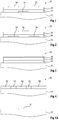
- FIGS. 5A to 5C illustrate successive steps of an embodiment of a method for manufacturing the field effect transistor shown in figure 1 .
- the figure 5A represents the structure obtained after the formation of the conductive portion 14 on the substrate 12.
- the conductive portion 14 can be deposited by screen printing or by ink jet.
- the figure 5B represents the structure obtained after the formation of the insulating layer 16 using a sol-gel process.
- the formation of the insulating layer 16 may comprise a step of preparing a sol containing the metal oxide composing the layer 16, a step of depositing the sol and a step of drying the gel.
- the step of preparing the soil can comprise the preparation of a solution comprising precursors of the metal oxide.
- the precursors can be metal alkoxides and / or metal salts.
- the precursor of zinc can be zinc acetate dihydrate (Zn (CH 3 COO) 2 .2H 2 O)
- the precursor of gallium can be hydrated gallium nitrate (Ga (NO 3 ) 3 .xH 2 O)
- the precursor of indium can be hydrated indium acetate (In (CH 3 COO) 3 .H 2 O)
- these precursors may be in the form of powders.
- the precursors are added to a solvent so as to form the sol.
- the soil may further include a dispersing agent. The hydrolysis reactions of the precursors and of the condensation of the hydrolysed compounds lead to the formation of a three-dimensional network of the metal oxide.
- the step of forming the layer 16 is carried out before obtaining the gel, when the sol has the desired viscosity.
- the gel is translucent and does not include agglomerates visible to the naked eye.
- the step of preparing the soil can be carried out at a temperature between 20 ° C and 100 ° C.
- the process for forming the layer 16 can correspond to a so-called additive process, for example by direct printing of the soil at the desired locations, for example by ink jet printing, rotogravure printing, screen printing, flexography, spray coating (in English spray coating) or drop deposit (in English drop-casting).
- the method for forming the layer 16 may correspond to a so-called subtractive method, in which the soil is deposited on the entire structure and in which the unused portions are then removed, for example by photolithography or laser ablation.
- deposition on the entire structure can be carried out by spinning deposition, spray coating, heliography, die coating (in English slot-die coating), blade coating (in English blade-coating ), flexography or serigraphy.
- the drying step is carried out at a temperature below a second threshold temperature below which an electrically insulating material is obtained.
- the second threshold temperature is of the order of 350 ° C and the drying step is carried out at a temperature between 200 ° C and 350 ° C, preferably between 250 ° C and 350 ° C.
- the drying time can vary from 4 minutes to 1 hour. Drying can be carried out in an oven in the ambient atmosphere.
- the material based on metal oxide finally obtained is an electrical insulator.
- One explanation would be that, due to the low drying temperature, the gel becomes disorganized by the migration of chemical species.
- certain elements, resulting from the precursors can be preserved in the gel and favor the insulating character.
- the figure 5C shows the structure obtained after the formation of the semiconductor layer 18 using a sol-gel process.
- the formation of the semiconductor layer 18 may include a step of preparing a sol containing the metal oxide composing the layer 18, a step of depositing the sol and a step of drying the gel.
- the floor can be prepared as described above in connection with the formation of the insulating layer 16.
- the floor used for the production of the insulation layer 16 has the same composition as the floor used for the production of the layer semiconductor 18.
- the sol used for the formation of the semiconductor layer 18 can be deposited according to the deposition methods described above for the formation of the insulating layer 16.
- each elementary semiconductor layer may have, after drying, a thickness of between 5 nm and 10 nm.
- the drying step is carried out at a temperature above a first threshold temperature, strictly above the second threshold temperature.
- the first threshold temperature is around 370 ° C and the drying step is carried out at a temperature between 370 ° C and 500 ° C, preferably between 400 ° C and 450 ° C.
- the drying time can vary from 4 minutes to 1 hour.
- the duration of the temperature rise from the deposition temperature of the soil to the drying temperature is less than a few seconds.
- the material based on metal oxide finally obtained is a semiconductor.
- One explanation would be that, due to the high drying temperature, the ordered structure of the gel freezes quickly.
- the elements originating from the precursors, which can promote the electrically insulating nature tend to leave the gel by evaporation substantially entirely.
- the inventors have demonstrated that, although the drying temperature used to produce the semiconductor layer 18 is higher than the drying temperature that was used to produce the insulating layer 16 in the previous step, the layer 16 retains its character as an electrical insulator. The insulating layer 16 can therefore be produced before the semiconductor layer 18.
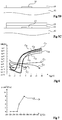
- the figure 6 represents evolution curves C 1 to Cg of the drain current Ids of a field effect transistor as a function of the gate voltage Vd, the transistor having the structure shown in figure 1 and having been produced according to the manufacturing process described above in relation to the Figures 5A to 5C .
- the substrate 12 was silicon and had a thickness of 750 ⁇ m.
- the conductive portions 20, 22 were made of gold and the portion 14 being made of aluminum.
- the portions 14, 20, 22 each had a thickness of 40 nm.
- the insulating layer 16 had a thickness of 100 nm.
- the semiconductor layer 18 had a thickness of 15 nm.
- the insulating layer 16 and the semiconductor layer 18 were produced from a sol prepared by mixing 30 mg of Zn powder (CH 3 COO) 2 .2H 2 O, 5 mg of Ga powder (NO 3 ) 3 . xH 2 O, 15 mg of powder of In (CH 3 COO) 3 .H 2 O, 10 ml of 2-methoxyethanol and 0.5 ml of ethanolamine. The solution was stirred for 12 hours at 70 ° C.
- the insulating layer 16 was deposited by ink jet printing in one go.
- the semiconductor layer 18 was deposited by ink jet printing by several successive deposits, each deposit being followed by a drying step before the next deposit.
- the channel length of the transistor was 20 ⁇ m.
- the drying temperature for the formation of the insulating layer 16 was 300 ° C. and the drying time for the formation of the insulating layer 16 was 1 hour for all the curves C 1 to Cg.
- the drying time for the formation of the semiconductor layer 18 was 450 ° C for all the curves C 1 to Cg.
- Table (1) below indicates, for each curve C 1 to Cg, the drying temperature used for the formation of the semiconductor layer 18 and the voltage Vds applied between the drain and the source of the transistor.
- the curves C 4 to Cg are characteristic of a field effect transistor, which clearly reflects the fact that the layer 16 is composed of an insulating material while the layer 18 is composed of a semiconductor material.
- the curves C 1 to C 3 show an absence of conduction of the MOS transistor, which means that the material making up the layer 18 does not have a semiconductor behavior but an insulator.
- the figure 7 represents an evolution curve D of the mobility ⁇ of the electrons in the semiconductor layer 18 as a function of the drying temperature used for the formation of this layer, the layer 18 having been prepared according to the method described above in relation to the figure 6 .
- the ⁇ mobility of the electrons was substantially equal to 0 when the drying temperature of layer 18 was less than 350 ° C and the ⁇ mobility of electrons was greater than 4 cm 2 / (Vs) when the drying temperature of layer 18 was greater than 370 ° C. This means that the material making up the layer 18 behaves as an electrical insulator when the drying temperature for the formation of the layer 18 is less than about 350 ° C and behaves like a semiconductor when the drying temperature for the formation of the layer is more than about 370 ° C.
- FIGS. 8A to 8C are sectional views of structures obtained at successive stages of an embodiment of a method of manufacturing the electronic device 60 represented in figure 4 .
- the figure 8A represents the structure obtained after the deposition of a layer 70 of a soil as described above on the substrate 62.
- the figure 8B shows the structure obtained after a local heating step of the layer 70 to form the semiconductor portions 64.
- the heating step may consist of briefly heating the layer 70 at the locations where semiconductor portions 64 are desired.
- Local heating can be achieved by a laser, in particular an excimer laser with a power of the order of 100 watts.
- Local heating can be achieved by ultraviolet (UV) radiation through a mask, in particular at least a short pulse of ultraviolet using the equipment marketed under the name PulseForge by the company Novacentrix or under the 'Sinteron 2000 appellation by Xenon Corporation.
- UV radiation is meant radiation whose wavelengths are, at least in part, between 200 nm and 400 nm.
- ultraviolet radiation is applied with short pulses, for example between 500 ⁇ s and 3 ms, with a fluence between 1 J / cm 2 and 30 J / cm 2 .
- the temperature of the semiconductor portions 64 in the layer 70 is brought very briefly to a temperature above 370 ° C.
- the heating is sufficiently intense and brief so that the temperature of the rest of the layer 70 does not rise above 370 ° C.
- the figure 8C represents the structure obtained after an overall heating step of the layer 70 at a temperature below 350 ° C. so as to form the insulating portions 66.
- the operations described above in relation to the Figures 8A to 8C can be repeated several times to obtain semiconductor portions 64 having the desired thickness.
Landscapes
- Thin Film Transistor (AREA)
Claims (12)
- Ein Verfahren zur Herstellung einer elektronischen Einrichtung (10; 30; 50; 60), das Folgendes aufweist:
Bilden mindestens eines ersten Abschnitts (18; 38; 54; 64) und eines zweiten Abschnitts (16; 40; 56; 66) auf der Basis eines Metalloxids durch ein Sol-Gel-Verfahren, Erhitzen des ersten Abschnitts auf eine Temperatur, die höher als eine erste Temperatur ist, so dass der erste Abschnitt zu einem Halbleiter wird, und das Erhitzen des zweiten Abschnitts auf eine Temperatur, die niedriger als eine zweite Temperatur ist, wobei die zweite Temperatur niedriger als die erste Temperatur ist, so dass der zweite Abschnitt elektrisch isolierend wird. - Verfahren nach Anspruch 1, wobei vor dem Erhitzen der erste Abschnitt und der zweite Abschnitt die gleiche Zusammensetzung haben.
- Verfahren nach Anspruch 1 oder 2, das die folgenden aufeinanderfolgenden Schritte aufweist:(a) Bilden des zweiten Abschnitts (16; 40; 56) durch ein Sol-Gel-Verfahren und Erhitzen des zweiten Abschnitts auf eine Temperatur, die niedriger als die zweite Temperatur ist; und(b) Bilden des ersten Abschnitts (18; 38; 54) durch ein Sol-Gel-Verfahren und Erhitzen des ersten Abschnitts auf eine Temperatur, die höher als die erste Temperatur ist.
- Verfahren nach Anspruch 1 oder 2, das die folgenden Schritte aufweist:Bilden einer Schicht (70) auf der Basis des Metalloxids durch ein Sol-Gel-Verfahren;lokales Erhitzen der Schicht auf eine Temperatur, die höher als die erste Temperatur ist, um den ersten Abschnitt (64) zu bilden; undErhitzen der Schicht auf eine Temperatur, die niedriger als die zweite Temperatur ist, um den zweiten Abschnitt (66) zu bilden.
- Verfahren nach Anspruch 4, wobei der lokale Erhitzungsschritt durch Laser- oder Ultraviolettstrahlung durchgeführt wird.
- Verfahren nach einem der Ansprüche 1 bis 5, wobei das Metalloxid aus der Gruppe ausgewählt wird, die Folgendes aufweist: Zinkoxid (ZnO), Indiumoxid (In203), Indiumzinkoxid (In-Zn-O), In-X-Zn-O-Oxide, wobei X aus der Gruppe ausgewählt wird, die Gallium (Ga), Antimon (Sb), Zinn (Sn), Magnesium (Mg), Beryllium (Be), Yttrium (Y), Silber (Ag), Aluminium (Al), Kalzium (Ca) und Nickel (Ni) aufweist, und Sn-X-Zn-O-Oxide, wobei X aus der Gruppe ausgewählt ist, die Gallium (Ga), Antimon (Sb), Magnesium (Mg), Beryllium (Be), Yttrium (Y), Silber (Ag), Aluminium (Al), Kalzium (Ca) und Nickel (Ni) aufweist.
- Eine elektronische Einrichtung (10; 30; 50; 60), die nach dem Verfahren nach einem der Ansprüche 1 bis 6 hergestellt wurde.
- Elektronische Einrichtung nach Anspruch 7, wobei der erste Abschnitt (18; 38; 54; 64) mit dem zweiten Abschnitt (16; 40; 56; 66) in Kontakt ist.
- Elektronische Einrichtung nach Anspruch 8, die auf einem Substrat (12; 32; 52) einen Stapel aus dem ersten Abschnitt (18; 38; 54) und dem zweiten Abschnitt (16; 40; 56) aufweist.
- Elektronische Einrichtung nach Anspruch 8 oder 9, wobei der erste Abschnitt (64) und der zweite Abschnitt (66) mit einem Substrat (62) in Kontakt sind.
- Elektronische Einrichtung nach Anspruch 8 oder 9, die einen Feldeffekttransistor aufweist, der einen Gate-Isolator, der dem zweiten Abschnitt (16; 40) entspricht, und einen im ersten Abschnitt (18; 38) gebildeten Kanalbereich aufweist.
- Elektronische Einrichtung nach Anspruch 8 oder 9 die einen MIS-Kondensator aufweist, der eine erste und eine zweite Elektrode (54, 58) aufweist, die durch einen dielektrischen Abschnitt (56) getrennt sind, wobei der erste Abschnitt der ersten Elektrode oder der zweiten Elektrode entspricht und der zweite Abschnitt (56) dem dielektrischen Abschnitt entspricht.
Applications Claiming Priority (2)
| Application Number | Priority Date | Filing Date | Title |
|---|---|---|---|
| FR1457328A FR3024589B1 (fr) | 2014-07-29 | 2014-07-29 | Dispositif electronique et son procede de fabrication |
| PCT/FR2015/052042 WO2016016554A1 (fr) | 2014-07-29 | 2015-07-23 | Dispositif electronique et son procede de fabrication |
Publications (2)
| Publication Number | Publication Date |
|---|---|
| EP3175484A1 EP3175484A1 (de) | 2017-06-07 |
| EP3175484B1 true EP3175484B1 (de) | 2020-05-27 |
Family
ID=51519131
Family Applications (1)
| Application Number | Title | Priority Date | Filing Date |
|---|---|---|---|
| EP15753728.3A Active EP3175484B1 (de) | 2014-07-29 | 2015-07-23 | Elektronisches bauelement und dessen herstellungsverfahren |
Country Status (4)
| Country | Link |
|---|---|
| US (1) | US10615033B2 (de) |
| EP (1) | EP3175484B1 (de) |
| FR (1) | FR3024589B1 (de) |
| WO (1) | WO2016016554A1 (de) |
Family Cites Families (14)
| Publication number | Priority date | Publication date | Assignee | Title |
|---|---|---|---|---|
| FR1457328A (fr) | 1965-06-09 | 1966-01-24 | Assemblage en nappes notamment de fils, fibres, mèches et tresses | |
| KR100212534B1 (ko) * | 1997-08-12 | 1999-08-02 | 이서봉 | 졸-겔 조성물 및 이로부터 제조된 고분자 이온 전도막 |
| JP4089858B2 (ja) * | 2000-09-01 | 2008-05-28 | 国立大学法人東北大学 | 半導体デバイス |
| US20070098905A1 (en) * | 2004-06-17 | 2007-05-03 | Electricite De France Service National | Method for preparing metal oxide layers |
| US20060003485A1 (en) * | 2004-06-30 | 2006-01-05 | Hoffman Randy L | Devices and methods of making the same |
| US20070037346A1 (en) * | 2005-02-22 | 2007-02-15 | Grant Robert W | Rapid thermal annealing of targeted thin film layers |
| JP5196870B2 (ja) * | 2007-05-23 | 2013-05-15 | キヤノン株式会社 | 酸化物半導体を用いた電子素子及びその製造方法 |
| JP5423396B2 (ja) * | 2007-12-20 | 2014-02-19 | コニカミノルタ株式会社 | 電子デバイスおよび電子デバイスの製造方法 |
| JPWO2012008041A1 (ja) * | 2010-07-12 | 2013-09-05 | 株式会社ユーテック | 強誘電体膜、ゾルゲル溶液、成膜方法及び強誘電体膜の製造方法 |
| JPWO2012043338A1 (ja) * | 2010-09-28 | 2014-02-06 | 凸版印刷株式会社 | 薄膜トランジスタ及びその製造方法、薄膜トランジスタを備える画像表示装置 |
| JP5880211B2 (ja) * | 2012-03-29 | 2016-03-08 | 三菱マテリアル株式会社 | フェライト薄膜形成用組成物及びフェライト薄膜の形成方法 |
| US11133118B2 (en) * | 2012-05-22 | 2021-09-28 | University Of Massachusetts | Patterned nanoparticle structures |
| US9356156B2 (en) * | 2013-05-24 | 2016-05-31 | Cbrite Inc. | Stable high mobility MOTFT and fabrication at low temperature |
| KR20150012874A (ko) * | 2013-07-26 | 2015-02-04 | 삼성디스플레이 주식회사 | 박막 트랜지스터 및 이의 제조 방법 및 평판 표시 장치용 백플레인의 제조 방법. |
-
2014
- 2014-07-29 FR FR1457328A patent/FR3024589B1/fr not_active Expired - Fee Related
-
2015
- 2015-07-23 EP EP15753728.3A patent/EP3175484B1/de active Active
- 2015-07-23 US US15/328,395 patent/US10615033B2/en active Active
- 2015-07-23 WO PCT/FR2015/052042 patent/WO2016016554A1/fr not_active Ceased
Non-Patent Citations (1)
| Title |
|---|
| None * |
Also Published As
| Publication number | Publication date |
|---|---|
| WO2016016554A1 (fr) | 2016-02-04 |
| FR3024589B1 (fr) | 2017-12-08 |
| EP3175484A1 (de) | 2017-06-07 |
| FR3024589A1 (fr) | 2016-02-05 |
| US20170213728A1 (en) | 2017-07-27 |
| US10615033B2 (en) | 2020-04-07 |
Similar Documents
| Publication | Publication Date | Title |
|---|---|---|
| US7507618B2 (en) | Method for making electronic devices using metal oxide nanoparticles | |
| FR3043836B1 (fr) | Dispositif electronique et son procede de fabrication | |
| JP5331382B2 (ja) | 半導体素子の製造方法 | |
| US9142696B2 (en) | Solar cells with silicon nanoparticles that are coated with nanoparticle passivation film | |
| US8114705B2 (en) | Electrically-conductive inorganic coating, method for producing the coating, circuit board, and semiconductor apparatus | |
| JP2024150628A (ja) | 素子の製造方法 | |
| EP3175484B1 (de) | Elektronisches bauelement und dessen herstellungsverfahren | |
| US9536912B2 (en) | Method of transferring thin film, method of manufacturing thin film transistor, method of forming pixel electrode of liquid crystal display device | |
| JP6396598B1 (ja) | 半導体装置の製造方法 | |
| CN1951162B (zh) | 元件配置基板及其制备方法 | |
| KR20210065018A (ko) | 이차원 소재의 박리 방법 및 이를 이용한 광 감응 소자의 제조 방법 | |
| JP2006032917A5 (de) | ||
| WO2017134808A1 (ja) | 半導体装置の製造方法 | |
| Ito et al. | Formulation and characterization of screen printable dopant ink for fabrication of polysilicon TFTs | |
| FR3019381A1 (fr) | Actionneur electroactif et procede de realisation | |
| WO2016016552A1 (fr) | Composant electronique comprenant une portion d'un oxyde semiconducteur et son procede de fabrication | |
| FR3024588A1 (fr) | Dispositif electronique et son procede de fabrication | |
| KR102218890B1 (ko) | 연속 광소결 박막트랜지스터 제조방법 | |
| JP2009033003A (ja) | 薄膜素子とその製造方法、半導体装置 | |
| JP4883259B2 (ja) | 半導体装置の製造方法 | |
| JP6228414B2 (ja) | 複合膜の製造方法 | |
| EP2747155A1 (de) | Herstellungsverfahren für eine Struktur des Typs MIS, im besonderen für eine Leuchtdiode | |
| TW201710198A (zh) | 用於太陽能電池製程之導電漿料 | |
| EP2539938A1 (de) | Waferäquivalent, verfahren zu dessen herstellung sowie verwendung |
Legal Events
| Date | Code | Title | Description |
|---|---|---|---|
| STAA | Information on the status of an ep patent application or granted ep patent |
Free format text: STATUS: THE INTERNATIONAL PUBLICATION HAS BEEN MADE |
|
| 17P | Request for examination filed |
Effective date: 20170120 |
|
| AK | Designated contracting states |
Kind code of ref document: A1 Designated state(s): AL AT BE BG CH CY CZ DE DK EE ES FI FR GB GR HR HU IE IS IT LI LT LU LV MC MK MT NL NO PL PT RO RS SE SI SK SM TR |
|
| AX | Request for extension of the european patent |
Extension state: BA ME |
|
| PUAI | Public reference made under article 153(3) epc to a published international application that has entered the european phase |
Free format text: ORIGINAL CODE: 0009012 |
|
| STAA | Information on the status of an ep patent application or granted ep patent |
Free format text: STATUS: REQUEST FOR EXAMINATION WAS MADE |
|
| RIN1 | Information on inventor provided before grant (corrected) |
Inventor name: COPPARD, ROMAIN Inventor name: BENWADIH, MOHAMMED |
|
| DAV | Request for validation of the european patent (deleted) | ||
| DAX | Request for extension of the european patent (deleted) | ||
| STAA | Information on the status of an ep patent application or granted ep patent |
Free format text: STATUS: EXAMINATION IS IN PROGRESS |
|
| 17Q | First examination report despatched |
Effective date: 20190403 |
|
| GRAP | Despatch of communication of intention to grant a patent |
Free format text: ORIGINAL CODE: EPIDOSNIGR1 |
|
| STAA | Information on the status of an ep patent application or granted ep patent |
Free format text: STATUS: GRANT OF PATENT IS INTENDED |
|
| INTG | Intention to grant announced |
Effective date: 20200225 |
|
| GRAS | Grant fee paid |
Free format text: ORIGINAL CODE: EPIDOSNIGR3 |
|
| GRAA | (expected) grant |
Free format text: ORIGINAL CODE: 0009210 |
|
| STAA | Information on the status of an ep patent application or granted ep patent |
Free format text: STATUS: THE PATENT HAS BEEN GRANTED |
|
| AK | Designated contracting states |
Kind code of ref document: B1 Designated state(s): AL AT BE BG CH CY CZ DE DK EE ES FI FR GB GR HR HU IE IS IT LI LT LU LV MC MK MT NL NO PL PT RO RS SE SI SK SM TR |
|
| REG | Reference to a national code |
Ref country code: GB Ref legal event code: FG4D Free format text: NOT ENGLISH |
|
| REG | Reference to a national code |
Ref country code: CH Ref legal event code: EP |
|
| REG | Reference to a national code |
Ref country code: DE Ref legal event code: R096 Ref document number: 602015053367 Country of ref document: DE |
|
| REG | Reference to a national code |
Ref country code: AT Ref legal event code: REF Ref document number: 1275465 Country of ref document: AT Kind code of ref document: T Effective date: 20200615 |
|
| REG | Reference to a national code |
Ref country code: LT Ref legal event code: MG4D |
|
| PG25 | Lapsed in a contracting state [announced via postgrant information from national office to epo] |
Ref country code: FI Free format text: LAPSE BECAUSE OF FAILURE TO SUBMIT A TRANSLATION OF THE DESCRIPTION OR TO PAY THE FEE WITHIN THE PRESCRIBED TIME-LIMIT Effective date: 20200527 Ref country code: GR Free format text: LAPSE BECAUSE OF FAILURE TO SUBMIT A TRANSLATION OF THE DESCRIPTION OR TO PAY THE FEE WITHIN THE PRESCRIBED TIME-LIMIT Effective date: 20200828 Ref country code: PT Free format text: LAPSE BECAUSE OF FAILURE TO SUBMIT A TRANSLATION OF THE DESCRIPTION OR TO PAY THE FEE WITHIN THE PRESCRIBED TIME-LIMIT Effective date: 20200928 Ref country code: LT Free format text: LAPSE BECAUSE OF FAILURE TO SUBMIT A TRANSLATION OF THE DESCRIPTION OR TO PAY THE FEE WITHIN THE PRESCRIBED TIME-LIMIT Effective date: 20200527 Ref country code: NO Free format text: LAPSE BECAUSE OF FAILURE TO SUBMIT A TRANSLATION OF THE DESCRIPTION OR TO PAY THE FEE WITHIN THE PRESCRIBED TIME-LIMIT Effective date: 20200827 Ref country code: IS Free format text: LAPSE BECAUSE OF FAILURE TO SUBMIT A TRANSLATION OF THE DESCRIPTION OR TO PAY THE FEE WITHIN THE PRESCRIBED TIME-LIMIT Effective date: 20200927 Ref country code: SE Free format text: LAPSE BECAUSE OF FAILURE TO SUBMIT A TRANSLATION OF THE DESCRIPTION OR TO PAY THE FEE WITHIN THE PRESCRIBED TIME-LIMIT Effective date: 20200527 |
|
| REG | Reference to a national code |
Ref country code: NL Ref legal event code: MP Effective date: 20200527 |
|
| PG25 | Lapsed in a contracting state [announced via postgrant information from national office to epo] |
Ref country code: BG Free format text: LAPSE BECAUSE OF FAILURE TO SUBMIT A TRANSLATION OF THE DESCRIPTION OR TO PAY THE FEE WITHIN THE PRESCRIBED TIME-LIMIT Effective date: 20200827 Ref country code: RS Free format text: LAPSE BECAUSE OF FAILURE TO SUBMIT A TRANSLATION OF THE DESCRIPTION OR TO PAY THE FEE WITHIN THE PRESCRIBED TIME-LIMIT Effective date: 20200527 Ref country code: HR Free format text: LAPSE BECAUSE OF FAILURE TO SUBMIT A TRANSLATION OF THE DESCRIPTION OR TO PAY THE FEE WITHIN THE PRESCRIBED TIME-LIMIT Effective date: 20200527 Ref country code: LV Free format text: LAPSE BECAUSE OF FAILURE TO SUBMIT A TRANSLATION OF THE DESCRIPTION OR TO PAY THE FEE WITHIN THE PRESCRIBED TIME-LIMIT Effective date: 20200527 |
|
| REG | Reference to a national code |
Ref country code: AT Ref legal event code: MK05 Ref document number: 1275465 Country of ref document: AT Kind code of ref document: T Effective date: 20200527 |
|
| PG25 | Lapsed in a contracting state [announced via postgrant information from national office to epo] |
Ref country code: AL Free format text: LAPSE BECAUSE OF FAILURE TO SUBMIT A TRANSLATION OF THE DESCRIPTION OR TO PAY THE FEE WITHIN THE PRESCRIBED TIME-LIMIT Effective date: 20200527 Ref country code: NL Free format text: LAPSE BECAUSE OF FAILURE TO SUBMIT A TRANSLATION OF THE DESCRIPTION OR TO PAY THE FEE WITHIN THE PRESCRIBED TIME-LIMIT Effective date: 20200527 |
|
| PG25 | Lapsed in a contracting state [announced via postgrant information from national office to epo] |
Ref country code: ES Free format text: LAPSE BECAUSE OF FAILURE TO SUBMIT A TRANSLATION OF THE DESCRIPTION OR TO PAY THE FEE WITHIN THE PRESCRIBED TIME-LIMIT Effective date: 20200527 Ref country code: AT Free format text: LAPSE BECAUSE OF FAILURE TO SUBMIT A TRANSLATION OF THE DESCRIPTION OR TO PAY THE FEE WITHIN THE PRESCRIBED TIME-LIMIT Effective date: 20200527 Ref country code: DK Free format text: LAPSE BECAUSE OF FAILURE TO SUBMIT A TRANSLATION OF THE DESCRIPTION OR TO PAY THE FEE WITHIN THE PRESCRIBED TIME-LIMIT Effective date: 20200527 Ref country code: EE Free format text: LAPSE BECAUSE OF FAILURE TO SUBMIT A TRANSLATION OF THE DESCRIPTION OR TO PAY THE FEE WITHIN THE PRESCRIBED TIME-LIMIT Effective date: 20200527 Ref country code: RO Free format text: LAPSE BECAUSE OF FAILURE TO SUBMIT A TRANSLATION OF THE DESCRIPTION OR TO PAY THE FEE WITHIN THE PRESCRIBED TIME-LIMIT Effective date: 20200527 Ref country code: CZ Free format text: LAPSE BECAUSE OF FAILURE TO SUBMIT A TRANSLATION OF THE DESCRIPTION OR TO PAY THE FEE WITHIN THE PRESCRIBED TIME-LIMIT Effective date: 20200527 Ref country code: SM Free format text: LAPSE BECAUSE OF FAILURE TO SUBMIT A TRANSLATION OF THE DESCRIPTION OR TO PAY THE FEE WITHIN THE PRESCRIBED TIME-LIMIT Effective date: 20200527 Ref country code: IT Free format text: LAPSE BECAUSE OF FAILURE TO SUBMIT A TRANSLATION OF THE DESCRIPTION OR TO PAY THE FEE WITHIN THE PRESCRIBED TIME-LIMIT Effective date: 20200527 |
|
| PG25 | Lapsed in a contracting state [announced via postgrant information from national office to epo] |
Ref country code: MC Free format text: LAPSE BECAUSE OF FAILURE TO SUBMIT A TRANSLATION OF THE DESCRIPTION OR TO PAY THE FEE WITHIN THE PRESCRIBED TIME-LIMIT Effective date: 20200527 Ref country code: SK Free format text: LAPSE BECAUSE OF FAILURE TO SUBMIT A TRANSLATION OF THE DESCRIPTION OR TO PAY THE FEE WITHIN THE PRESCRIBED TIME-LIMIT Effective date: 20200527 Ref country code: PL Free format text: LAPSE BECAUSE OF FAILURE TO SUBMIT A TRANSLATION OF THE DESCRIPTION OR TO PAY THE FEE WITHIN THE PRESCRIBED TIME-LIMIT Effective date: 20200527 |
|
| REG | Reference to a national code |
Ref country code: CH Ref legal event code: PL |
|
| REG | Reference to a national code |
Ref country code: DE Ref legal event code: R097 Ref document number: 602015053367 Country of ref document: DE |
|
| PLBE | No opposition filed within time limit |
Free format text: ORIGINAL CODE: 0009261 |
|
| STAA | Information on the status of an ep patent application or granted ep patent |
Free format text: STATUS: NO OPPOSITION FILED WITHIN TIME LIMIT |
|
| REG | Reference to a national code |
Ref country code: BE Ref legal event code: MM Effective date: 20200731 |
|
| PG25 | Lapsed in a contracting state [announced via postgrant information from national office to epo] |
Ref country code: LU Free format text: LAPSE BECAUSE OF NON-PAYMENT OF DUE FEES Effective date: 20200723 Ref country code: LI Free format text: LAPSE BECAUSE OF NON-PAYMENT OF DUE FEES Effective date: 20200731 Ref country code: CH Free format text: LAPSE BECAUSE OF NON-PAYMENT OF DUE FEES Effective date: 20200731 |
|
| 26N | No opposition filed |
Effective date: 20210302 |
|
| PG25 | Lapsed in a contracting state [announced via postgrant information from national office to epo] |
Ref country code: BE Free format text: LAPSE BECAUSE OF NON-PAYMENT OF DUE FEES Effective date: 20200731 Ref country code: SI Free format text: LAPSE BECAUSE OF FAILURE TO SUBMIT A TRANSLATION OF THE DESCRIPTION OR TO PAY THE FEE WITHIN THE PRESCRIBED TIME-LIMIT Effective date: 20200527 |
|
| PG25 | Lapsed in a contracting state [announced via postgrant information from national office to epo] |
Ref country code: IE Free format text: LAPSE BECAUSE OF NON-PAYMENT OF DUE FEES Effective date: 20200723 |
|
| PG25 | Lapsed in a contracting state [announced via postgrant information from national office to epo] |
Ref country code: TR Free format text: LAPSE BECAUSE OF FAILURE TO SUBMIT A TRANSLATION OF THE DESCRIPTION OR TO PAY THE FEE WITHIN THE PRESCRIBED TIME-LIMIT Effective date: 20200527 Ref country code: MT Free format text: LAPSE BECAUSE OF FAILURE TO SUBMIT A TRANSLATION OF THE DESCRIPTION OR TO PAY THE FEE WITHIN THE PRESCRIBED TIME-LIMIT Effective date: 20200527 Ref country code: CY Free format text: LAPSE BECAUSE OF FAILURE TO SUBMIT A TRANSLATION OF THE DESCRIPTION OR TO PAY THE FEE WITHIN THE PRESCRIBED TIME-LIMIT Effective date: 20200527 |
|
| PG25 | Lapsed in a contracting state [announced via postgrant information from national office to epo] |
Ref country code: MK Free format text: LAPSE BECAUSE OF FAILURE TO SUBMIT A TRANSLATION OF THE DESCRIPTION OR TO PAY THE FEE WITHIN THE PRESCRIBED TIME-LIMIT Effective date: 20200527 |
|
| REG | Reference to a national code |
Ref country code: DE Ref legal event code: R079 Ref document number: 602015053367 Country of ref document: DE Free format text: PREVIOUS MAIN CLASS: H01L0029490000 Ipc: H10D0064660000 |
|
| PGFP | Annual fee paid to national office [announced via postgrant information from national office to epo] |
Ref country code: DE Payment date: 20250722 Year of fee payment: 11 |
|
| PGFP | Annual fee paid to national office [announced via postgrant information from national office to epo] |
Ref country code: GB Payment date: 20250724 Year of fee payment: 11 |
|
| PGFP | Annual fee paid to national office [announced via postgrant information from national office to epo] |
Ref country code: FR Payment date: 20250722 Year of fee payment: 11 |