EP3171389A1 - Light-emitting device - Google Patents
Light-emitting device Download PDFInfo
- Publication number
- EP3171389A1 EP3171389A1 EP15821750.5A EP15821750A EP3171389A1 EP 3171389 A1 EP3171389 A1 EP 3171389A1 EP 15821750 A EP15821750 A EP 15821750A EP 3171389 A1 EP3171389 A1 EP 3171389A1
- Authority
- EP
- European Patent Office
- Prior art keywords
- light
- discharge
- ceramic package
- emitting device
- couple
- Prior art date
- Legal status (The legal status is an assumption and is not a legal conclusion. Google has not performed a legal analysis and makes no representation as to the accuracy of the status listed.)
- Granted
Links
- 239000000919 ceramic Substances 0.000 claims abstract description 125
- 239000000843 powder Substances 0.000 claims abstract description 90
- 239000000463 material Substances 0.000 claims abstract description 67
- 239000011521 glass Substances 0.000 claims abstract description 61
- 230000000994 depressogenic effect Effects 0.000 claims abstract description 43
- 239000011261 inert gas Substances 0.000 claims abstract description 18
- 229910052574 oxide ceramic Inorganic materials 0.000 claims abstract description 17
- 239000011224 oxide ceramic Substances 0.000 claims abstract description 17
- 230000001747 exhibiting effect Effects 0.000 claims abstract description 11
- PNEYBMLMFCGWSK-UHFFFAOYSA-N aluminium oxide Inorganic materials [O-2].[O-2].[O-2].[Al+3].[Al+3] PNEYBMLMFCGWSK-UHFFFAOYSA-N 0.000 claims description 73
- 230000006698 induction Effects 0.000 claims description 41
- XLOMVQKBTHCTTD-UHFFFAOYSA-N Zinc monoxide Chemical compound [Zn]=O XLOMVQKBTHCTTD-UHFFFAOYSA-N 0.000 claims description 14
- VYPSYNLAJGMNEJ-UHFFFAOYSA-N Silicium dioxide Chemical compound O=[Si]=O VYPSYNLAJGMNEJ-UHFFFAOYSA-N 0.000 claims description 13
- 229910000416 bismuth oxide Inorganic materials 0.000 claims description 12
- TYIXMATWDRGMPF-UHFFFAOYSA-N dibismuth;oxygen(2-) Chemical compound [O-2].[O-2].[O-2].[Bi+3].[Bi+3] TYIXMATWDRGMPF-UHFFFAOYSA-N 0.000 claims description 12
- 229910052814 silicon oxide Inorganic materials 0.000 claims description 7
- 239000011787 zinc oxide Substances 0.000 claims description 7
- 230000007423 decrease Effects 0.000 abstract description 17
- 239000012298 atmosphere Substances 0.000 description 22
- QVGXLLKOCUKJST-UHFFFAOYSA-N atomic oxygen Chemical compound [O] QVGXLLKOCUKJST-UHFFFAOYSA-N 0.000 description 22
- 239000001301 oxygen Substances 0.000 description 22
- 229910052760 oxygen Inorganic materials 0.000 description 22
- 238000005304 joining Methods 0.000 description 17
- MCMNRKCIXSYSNV-UHFFFAOYSA-N Zirconium dioxide Chemical compound O=[Zr]=O MCMNRKCIXSYSNV-UHFFFAOYSA-N 0.000 description 15
- 239000007789 gas Substances 0.000 description 14
- 238000000034 method Methods 0.000 description 13
- CJJMLLCUQDSZIZ-UHFFFAOYSA-N oxobismuth Chemical class [Bi]=O CJJMLLCUQDSZIZ-UHFFFAOYSA-N 0.000 description 10
- WFKWXMTUELFFGS-UHFFFAOYSA-N tungsten Chemical compound [W] WFKWXMTUELFFGS-UHFFFAOYSA-N 0.000 description 10
- 229910052721 tungsten Inorganic materials 0.000 description 10
- 239000010937 tungsten Substances 0.000 description 10
- 230000002093 peripheral effect Effects 0.000 description 9
- 239000011230 binding agent Substances 0.000 description 8
- 238000010438 heat treatment Methods 0.000 description 7
- ZOKXTWBITQBERF-UHFFFAOYSA-N Molybdenum Chemical compound [Mo] ZOKXTWBITQBERF-UHFFFAOYSA-N 0.000 description 6
- 229910052750 molybdenum Inorganic materials 0.000 description 6
- 239000011733 molybdenum Substances 0.000 description 6
- BASFCYQUMIYNBI-UHFFFAOYSA-N platinum Chemical compound [Pt] BASFCYQUMIYNBI-UHFFFAOYSA-N 0.000 description 6
- 239000002904 solvent Substances 0.000 description 6
- 239000011810 insulating material Substances 0.000 description 5
- 229910052751 metal Inorganic materials 0.000 description 5
- 239000002184 metal Substances 0.000 description 5
- 239000007769 metal material Substances 0.000 description 5
- 239000012299 nitrogen atmosphere Substances 0.000 description 5
- TWNQGVIAIRXVLR-UHFFFAOYSA-N oxo(oxoalumanyloxy)alumane Chemical compound O=[Al]O[Al]=O TWNQGVIAIRXVLR-UHFFFAOYSA-N 0.000 description 5
- 238000007650 screen-printing Methods 0.000 description 5
- 229910010293 ceramic material Inorganic materials 0.000 description 4
- 239000010949 copper Substances 0.000 description 4
- JKWMSGQKBLHBQQ-UHFFFAOYSA-N diboron trioxide Chemical compound O=BOB=O JKWMSGQKBLHBQQ-UHFFFAOYSA-N 0.000 description 4
- 238000005259 measurement Methods 0.000 description 4
- 230000008569 process Effects 0.000 description 4
- 230000001603 reducing effect Effects 0.000 description 4
- 229910052681 coesite Inorganic materials 0.000 description 3
- 229910052906 cristobalite Inorganic materials 0.000 description 3
- 229910052746 lanthanum Inorganic materials 0.000 description 3
- FZLIPJUXYLNCLC-UHFFFAOYSA-N lanthanum atom Chemical compound [La] FZLIPJUXYLNCLC-UHFFFAOYSA-N 0.000 description 3
- WPBNNNQJVZRUHP-UHFFFAOYSA-L manganese(2+);methyl n-[[2-(methoxycarbonylcarbamothioylamino)phenyl]carbamothioyl]carbamate;n-[2-(sulfidocarbothioylamino)ethyl]carbamodithioate Chemical compound [Mn+2].[S-]C(=S)NCCNC([S-])=S.COC(=O)NC(=S)NC1=CC=CC=C1NC(=S)NC(=O)OC WPBNNNQJVZRUHP-UHFFFAOYSA-L 0.000 description 3
- 238000004519 manufacturing process Methods 0.000 description 3
- 238000002156 mixing Methods 0.000 description 3
- 230000003647 oxidation Effects 0.000 description 3
- 238000007254 oxidation reaction Methods 0.000 description 3
- 239000002245 particle Substances 0.000 description 3
- 229910052697 platinum Inorganic materials 0.000 description 3
- 230000009467 reduction Effects 0.000 description 3
- 239000000377 silicon dioxide Substances 0.000 description 3
- 229910052682 stishovite Inorganic materials 0.000 description 3
- 229910052712 strontium Inorganic materials 0.000 description 3
- CIOAGBVUUVVLOB-UHFFFAOYSA-N strontium atom Chemical compound [Sr] CIOAGBVUUVVLOB-UHFFFAOYSA-N 0.000 description 3
- 229910052905 tridymite Inorganic materials 0.000 description 3
- QGZKDVFQNNGYKY-UHFFFAOYSA-N Ammonia Chemical compound N QGZKDVFQNNGYKY-UHFFFAOYSA-N 0.000 description 2
- XKRFYHLGVUSROY-UHFFFAOYSA-N Argon Chemical compound [Ar] XKRFYHLGVUSROY-UHFFFAOYSA-N 0.000 description 2
- IJGRMHOSHXDMSA-UHFFFAOYSA-N Atomic nitrogen Chemical compound N#N IJGRMHOSHXDMSA-UHFFFAOYSA-N 0.000 description 2
- RYGMFSIKBFXOCR-UHFFFAOYSA-N Copper Chemical compound [Cu] RYGMFSIKBFXOCR-UHFFFAOYSA-N 0.000 description 2
- UFHFLCQGNIYNRP-UHFFFAOYSA-N Hydrogen Chemical compound [H][H] UFHFLCQGNIYNRP-UHFFFAOYSA-N 0.000 description 2
- DGAQECJNVWCQMB-PUAWFVPOSA-M Ilexoside XXIX Chemical compound C[C@@H]1CC[C@@]2(CC[C@@]3(C(=CC[C@H]4[C@]3(CC[C@@H]5[C@@]4(CC[C@@H](C5(C)C)OS(=O)(=O)[O-])C)C)[C@@H]2[C@]1(C)O)C)C(=O)O[C@H]6[C@@H]([C@H]([C@@H]([C@H](O6)CO)O)O)O.[Na+] DGAQECJNVWCQMB-PUAWFVPOSA-M 0.000 description 2
- WHXSMMKQMYFTQS-UHFFFAOYSA-N Lithium Chemical compound [Li] WHXSMMKQMYFTQS-UHFFFAOYSA-N 0.000 description 2
- 229910017309 Mo—Mn Inorganic materials 0.000 description 2
- ZLMJMSJWJFRBEC-UHFFFAOYSA-N Potassium Chemical compound [K] ZLMJMSJWJFRBEC-UHFFFAOYSA-N 0.000 description 2
- BQCADISMDOOEFD-UHFFFAOYSA-N Silver Chemical compound [Ag] BQCADISMDOOEFD-UHFFFAOYSA-N 0.000 description 2
- 230000009471 action Effects 0.000 description 2
- 229910052783 alkali metal Inorganic materials 0.000 description 2
- 150000001340 alkali metals Chemical class 0.000 description 2
- 229910000287 alkaline earth metal oxide Inorganic materials 0.000 description 2
- WMWLMWRWZQELOS-UHFFFAOYSA-N bismuth(iii) oxide Chemical compound O=[Bi]O[Bi]=O WMWLMWRWZQELOS-UHFFFAOYSA-N 0.000 description 2
- 229910052810 boron oxide Inorganic materials 0.000 description 2
- 229910052802 copper Inorganic materials 0.000 description 2
- 238000005286 illumination Methods 0.000 description 2
- 238000003384 imaging method Methods 0.000 description 2
- 238000003475 lamination Methods 0.000 description 2
- MRELNEQAGSRDBK-UHFFFAOYSA-N lanthanum(3+);oxygen(2-) Chemical compound [O-2].[O-2].[O-2].[La+3].[La+3] MRELNEQAGSRDBK-UHFFFAOYSA-N 0.000 description 2
- 229910052744 lithium Inorganic materials 0.000 description 2
- 229910052748 manganese Inorganic materials 0.000 description 2
- 239000011572 manganese Substances 0.000 description 2
- 238000002844 melting Methods 0.000 description 2
- 230000008018 melting Effects 0.000 description 2
- KDLHZDBZIXYQEI-UHFFFAOYSA-N palladium Substances [Pd] KDLHZDBZIXYQEI-UHFFFAOYSA-N 0.000 description 2
- SWELZOZIOHGSPA-UHFFFAOYSA-N palladium silver Chemical compound [Pd].[Ag] SWELZOZIOHGSPA-UHFFFAOYSA-N 0.000 description 2
- 229910052700 potassium Inorganic materials 0.000 description 2
- 239000011591 potassium Substances 0.000 description 2
- 229910052709 silver Inorganic materials 0.000 description 2
- 239000004332 silver Substances 0.000 description 2
- 239000002002 slurry Substances 0.000 description 2
- 229910052708 sodium Inorganic materials 0.000 description 2
- 239000011734 sodium Substances 0.000 description 2
- 108010053481 Antifreeze Proteins Proteins 0.000 description 1
- 229910052581 Si3N4 Inorganic materials 0.000 description 1
- 229910021529 ammonia Inorganic materials 0.000 description 1
- 229910052786 argon Inorganic materials 0.000 description 1
- 229910052797 bismuth Inorganic materials 0.000 description 1
- JCXGWMGPZLAOME-UHFFFAOYSA-N bismuth atom Chemical compound [Bi] JCXGWMGPZLAOME-UHFFFAOYSA-N 0.000 description 1
- 239000005388 borosilicate glass Substances 0.000 description 1
- BRPQOXSCLDDYGP-UHFFFAOYSA-N calcium oxide Chemical compound [O-2].[Ca+2] BRPQOXSCLDDYGP-UHFFFAOYSA-N 0.000 description 1
- 239000000292 calcium oxide Substances 0.000 description 1
- ODINCKMPIJJUCX-UHFFFAOYSA-N calcium oxide Inorganic materials [Ca]=O ODINCKMPIJJUCX-UHFFFAOYSA-N 0.000 description 1
- 230000015556 catabolic process Effects 0.000 description 1
- 229910000420 cerium oxide Inorganic materials 0.000 description 1
- 230000008859 change Effects 0.000 description 1
- 239000011248 coating agent Substances 0.000 description 1
- 238000000576 coating method Methods 0.000 description 1
- PMHQVHHXPFUNSP-UHFFFAOYSA-M copper(1+);methylsulfanylmethane;bromide Chemical compound Br[Cu].CSC PMHQVHHXPFUNSP-UHFFFAOYSA-M 0.000 description 1
- 229910052593 corundum Inorganic materials 0.000 description 1
- 230000003247 decreasing effect Effects 0.000 description 1
- 230000007547 defect Effects 0.000 description 1
- 238000013461 design Methods 0.000 description 1
- KZHJGOXRZJKJNY-UHFFFAOYSA-N dioxosilane;oxo(oxoalumanyloxy)alumane Chemical compound O=[Si]=O.O=[Si]=O.O=[Al]O[Al]=O.O=[Al]O[Al]=O.O=[Al]O[Al]=O KZHJGOXRZJKJNY-UHFFFAOYSA-N 0.000 description 1
- 238000007599 discharging Methods 0.000 description 1
- 238000007606 doctor blade method Methods 0.000 description 1
- 239000012777 electrically insulating material Substances 0.000 description 1
- 239000003822 epoxy resin Substances 0.000 description 1
- 230000002349 favourable effect Effects 0.000 description 1
- 238000010304 firing Methods 0.000 description 1
- 230000004907 flux Effects 0.000 description 1
- -1 for example Substances 0.000 description 1
- 230000009477 glass transition Effects 0.000 description 1
- 239000002241 glass-ceramic Substances 0.000 description 1
- 239000001307 helium Substances 0.000 description 1
- 229910052734 helium Inorganic materials 0.000 description 1
- SWQJXJOGLNCZEY-UHFFFAOYSA-N helium atom Chemical compound [He] SWQJXJOGLNCZEY-UHFFFAOYSA-N 0.000 description 1
- 239000001257 hydrogen Substances 0.000 description 1
- 229910052739 hydrogen Inorganic materials 0.000 description 1
- 238000009413 insulation Methods 0.000 description 1
- 229910052743 krypton Inorganic materials 0.000 description 1
- DNNSSWSSYDEUBZ-UHFFFAOYSA-N krypton atom Chemical compound [Kr] DNNSSWSSYDEUBZ-UHFFFAOYSA-N 0.000 description 1
- 238000010030 laminating Methods 0.000 description 1
- 239000000395 magnesium oxide Substances 0.000 description 1
- CPLXHLVBOLITMK-UHFFFAOYSA-N magnesium oxide Inorganic materials [Mg]=O CPLXHLVBOLITMK-UHFFFAOYSA-N 0.000 description 1
- AXZKOIWUVFPNLO-UHFFFAOYSA-N magnesium;oxygen(2-) Chemical compound [O-2].[Mg+2] AXZKOIWUVFPNLO-UHFFFAOYSA-N 0.000 description 1
- 238000000691 measurement method Methods 0.000 description 1
- 239000000203 mixture Substances 0.000 description 1
- 238000012986 modification Methods 0.000 description 1
- 230000004048 modification Effects 0.000 description 1
- 239000004570 mortar (masonry) Substances 0.000 description 1
- 229910052863 mullite Inorganic materials 0.000 description 1
- 229910052754 neon Inorganic materials 0.000 description 1
- GKAOGPIIYCISHV-UHFFFAOYSA-N neon atom Chemical compound [Ne] GKAOGPIIYCISHV-UHFFFAOYSA-N 0.000 description 1
- 229910052757 nitrogen Inorganic materials 0.000 description 1
- BMMGVYCKOGBVEV-UHFFFAOYSA-N oxo(oxoceriooxy)cerium Chemical compound [Ce]=O.O=[Ce]=O BMMGVYCKOGBVEV-UHFFFAOYSA-N 0.000 description 1
- SIWVEOZUMHYXCS-UHFFFAOYSA-N oxo(oxoyttriooxy)yttrium Chemical compound O=[Y]O[Y]=O SIWVEOZUMHYXCS-UHFFFAOYSA-N 0.000 description 1
- RVTZCBVAJQQJTK-UHFFFAOYSA-N oxygen(2-);zirconium(4+) Chemical compound [O-2].[O-2].[Zr+4] RVTZCBVAJQQJTK-UHFFFAOYSA-N 0.000 description 1
- 229920000647 polyepoxide Polymers 0.000 description 1
- 229920001225 polyester resin Polymers 0.000 description 1
- 239000004645 polyester resin Substances 0.000 description 1
- 238000007639 printing Methods 0.000 description 1
- 238000010298 pulverizing process Methods 0.000 description 1
- 238000004080 punching Methods 0.000 description 1
- 239000002994 raw material Substances 0.000 description 1
- 229920005989 resin Polymers 0.000 description 1
- 239000011347 resin Substances 0.000 description 1
- HBMJWWWQQXIZIP-UHFFFAOYSA-N silicon carbide Chemical compound [Si+]#[C-] HBMJWWWQQXIZIP-UHFFFAOYSA-N 0.000 description 1
- 229910010271 silicon carbide Inorganic materials 0.000 description 1
- LIVNPJMFVYWSIS-UHFFFAOYSA-N silicon monoxide Chemical class [Si-]#[O+] LIVNPJMFVYWSIS-UHFFFAOYSA-N 0.000 description 1
- HQVNEWCFYHHQES-UHFFFAOYSA-N silicon nitride Chemical compound N12[Si]34N5[Si]62N3[Si]51N64 HQVNEWCFYHHQES-UHFFFAOYSA-N 0.000 description 1
- 238000012360 testing method Methods 0.000 description 1
- 229910052724 xenon Inorganic materials 0.000 description 1
- FHNFHKCVQCLJFQ-UHFFFAOYSA-N xenon atom Chemical compound [Xe] FHNFHKCVQCLJFQ-UHFFFAOYSA-N 0.000 description 1
- 229910001845 yogo sapphire Inorganic materials 0.000 description 1
Images


Classifications
-
- H—ELECTRICITY
- H01—ELECTRIC ELEMENTS
- H01J—ELECTRIC DISCHARGE TUBES OR DISCHARGE LAMPS
- H01J61/00—Gas-discharge or vapour-discharge lamps
- H01J61/02—Details
- H01J61/30—Vessels; Containers
- H01J61/33—Special shape of cross-section, e.g. for producing cool spot
-
- H—ELECTRICITY
- H01—ELECTRIC ELEMENTS
- H01J—ELECTRIC DISCHARGE TUBES OR DISCHARGE LAMPS
- H01J61/00—Gas-discharge or vapour-discharge lamps
- H01J61/02—Details
- H01J61/025—Associated optical elements
-
- H—ELECTRICITY
- H01—ELECTRIC ELEMENTS
- H01J—ELECTRIC DISCHARGE TUBES OR DISCHARGE LAMPS
- H01J61/00—Gas-discharge or vapour-discharge lamps
- H01J61/02—Details
- H01J61/04—Electrodes; Screens; Shields
- H01J61/06—Main electrodes
- H01J61/067—Main electrodes for low-pressure discharge lamps
-
- H—ELECTRICITY
- H01—ELECTRIC ELEMENTS
- H01J—ELECTRIC DISCHARGE TUBES OR DISCHARGE LAMPS
- H01J61/00—Gas-discharge or vapour-discharge lamps
- H01J61/02—Details
- H01J61/04—Electrodes; Screens; Shields
- H01J61/06—Main electrodes
- H01J61/067—Main electrodes for low-pressure discharge lamps
- H01J61/0672—Main electrodes for low-pressure discharge lamps characterised by the construction of the electrode
-
- H—ELECTRICITY
- H01—ELECTRIC ELEMENTS
- H01J—ELECTRIC DISCHARGE TUBES OR DISCHARGE LAMPS
- H01J61/00—Gas-discharge or vapour-discharge lamps
- H01J61/02—Details
- H01J61/30—Vessels; Containers
- H01J61/302—Vessels; Containers characterised by the material of the vessel
-
- H—ELECTRICITY
- H01—ELECTRIC ELEMENTS
- H01J—ELECTRIC DISCHARGE TUBES OR DISCHARGE LAMPS
- H01J61/00—Gas-discharge or vapour-discharge lamps
- H01J61/02—Details
- H01J61/30—Vessels; Containers
- H01J61/305—Flat vessels or containers
-
- H—ELECTRICITY
- H01—ELECTRIC ELEMENTS
- H01J—ELECTRIC DISCHARGE TUBES OR DISCHARGE LAMPS
- H01J61/00—Gas-discharge or vapour-discharge lamps
- H01J61/02—Details
- H01J61/36—Seals between parts of vessels; Seals for leading-in conductors; Leading-in conductors
- H01J61/361—Seals between parts of vessel
-
- H—ELECTRICITY
- H01—ELECTRIC ELEMENTS
- H01J—ELECTRIC DISCHARGE TUBES OR DISCHARGE LAMPS
- H01J61/00—Gas-discharge or vapour-discharge lamps
- H01J61/02—Details
- H01J61/54—Igniting arrangements, e.g. promoting ionisation for starting
-
- H—ELECTRICITY
- H01—ELECTRIC ELEMENTS
- H01J—ELECTRIC DISCHARGE TUBES OR DISCHARGE LAMPS
- H01J61/00—Gas-discharge or vapour-discharge lamps
- H01J61/02—Details
- H01J61/54—Igniting arrangements, e.g. promoting ionisation for starting
- H01J61/545—Igniting arrangements, e.g. promoting ionisation for starting using an auxiliary electrode inside the vessel
-
- H—ELECTRICITY
- H01—ELECTRIC ELEMENTS
- H01J—ELECTRIC DISCHARGE TUBES OR DISCHARGE LAMPS
- H01J61/00—Gas-discharge or vapour-discharge lamps
- H01J61/70—Lamps with low-pressure unconstricted discharge having a cold pressure < 400 Torr
- H01J61/80—Lamps suitable only for intermittent operation, e.g. flash lamp
-
- H—ELECTRICITY
- H01—ELECTRIC ELEMENTS
- H01J—ELECTRIC DISCHARGE TUBES OR DISCHARGE LAMPS
- H01J9/00—Apparatus or processes specially adapted for the manufacture, installation, removal, maintenance of electric discharge tubes, discharge lamps, or parts thereof; Recovery of material from discharge tubes or lamps
- H01J9/24—Manufacture or joining of vessels, leading-in conductors or bases
- H01J9/26—Sealing together parts of vessels
- H01J9/265—Sealing together parts of vessels specially adapted for gas-discharge tubes or lamps
- H01J9/266—Sealing together parts of vessels specially adapted for gas-discharge tubes or lamps specially adapted for gas-discharge lamps
- H01J9/268—Sealing together parts of vessels specially adapted for gas-discharge tubes or lamps specially adapted for gas-discharge lamps the vessel being flat
-
- G—PHYSICS
- G03—PHOTOGRAPHY; CINEMATOGRAPHY; ANALOGOUS TECHNIQUES USING WAVES OTHER THAN OPTICAL WAVES; ELECTROGRAPHY; HOLOGRAPHY
- G03B—APPARATUS OR ARRANGEMENTS FOR TAKING PHOTOGRAPHS OR FOR PROJECTING OR VIEWING THEM; APPARATUS OR ARRANGEMENTS EMPLOYING ANALOGOUS TECHNIQUES USING WAVES OTHER THAN OPTICAL WAVES; ACCESSORIES THEREFOR
- G03B15/00—Special procedures for taking photographs; Apparatus therefor
- G03B15/02—Illuminating scene
- G03B15/03—Combinations of cameras with lighting apparatus; Flash units
- G03B15/05—Combinations of cameras with electronic flash apparatus; Electronic flash units
Definitions
- the present invention relates to a light-emitting device such for example as an electric-discharge lamp.
- a light-emitting device such for example as an electric-discharge lamp having a structure in which an inert gas is filled in a glass tube has been known.
- a couple of discharge electrodes are fixed to the glass tube with protruding from an end portion of the glass tube into a discharge space, and a discharge induction electrode is disposed on an outer periphery of the glass tube.
- An example of the electric-discharge lamp is disclosed in Japanese Unexamined Patent Publication JP-A 09-180677 (1997) .
- the light-emitting device such as an electric-discharge lamp is needed to be further miniaturized so as to mount the same to a portable terminal and the like.
- the light-emitting device having the conventional glass tube has a structure that is difficult to be made small.
- a structure of a light-emitting device which includes a package and a light transmitting member joined to the package and has a discharge space in a container member has been known.
- An example of the light-emitting device is disclosed in Japanese Unexamined Patent Publication JP-A 2011-96562 .
- the light-emitting device including the package and the light transmitting member joined to the package has a problem that a light emission amount decreases because the package and the light transmitting member are joined via a joining material and the light generated in the discharge space is thus likely to be absorbed by the joining material.
- the invention has been made in view of the above problems, and an object thereof is to provide a light-emitting device capable of suppressing a decrease in a light emission amount due to a joining material for joining a package and a light transmitting member.
- a light-emitting device includes a container member including a ceramic package provided with a depressed portion serving as a discharge space, and a light transmitting inorganic member which is attached to the ceramic package via a joining layer formed of a joining material so as to close the depressed portion; an inert gas encapsulated inside the discharge space; and a couple of discharge electrodes which are disposed in the depressed portion of the ceramic package so as to be spaced from each other, the joining material including glass exhibiting a white color, and oxide ceramic powder.
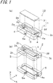
- a light-emitting device 10 according to an embodiment of the invention is described with reference to FIGS. 1 to 5 .
- the light-emitting device 10 is embedded in a portable terminal such as a smart phone or an imaging device such as a digital camera.
- the light-emitting device 10 can instantaneously generate a flash light in a larger amount of light by using a discharge action of a rare gas, for example, as compared to an LED.
- the light-emitting device 10 has a configuration as shown in FIGS. 1 to 5 , and includes a container member 1, an inert gas 6, and a couple of discharge electrodes 4.
- the container member 1 includes a ceramic package 2 provided with a depressed portion 2b serving as a discharge space and a light transmitting member 3, which is a light transmitting inorganic member which is joined to the ceramic package 2 via a joining layer 7a formed of a joining material 7 so as to close the depressed portion 2b.
- the couple of discharge electrodes 4 are disposed on opposite sidewalls 2a of the ceramic package 2 and has opposite parts 4b disposed to face each other.
- the joining material 7 comprises glass exhibiting a white color and oxide ceramic powder.
- a light emission direction of the light-emitting device 10 is a positive side of the Z direction.
- the light-emitting device 10 may have a discharge induction electrode 5 in the ceramic package 2 so as to easily start the discharge in the discharge space S.
- the light-emitting device 10 is configured so that the annular discharge induction electrode 5 is disposed in the ceramic package 2 so as to be below the couple of discharge electrodes 4 and surround the depressed portion 2b. Also, the opposite parts 4b of the couple of discharge electrodes 4 are positioned more inwardly than an inner periphery of the discharge induction electrode 5, as seen from a plan view.
- the light-emitting device 10 can be made smaller and easily generate the discharge between the couple of discharge electrodes 4. Also, since the container member 1 can sufficiently secure the discharge space S inside the ceramic package 2 and electrode areas of the discharge electrodes 4 can be made great, the light-emitting device 10 can effectively generate the discharge between the couple of discharge electrodes 4.
- the light-emitting device 10 has the annular discharge induction electrode 5, so that it is possible to ionize the entire inert gas 6, and particularly, to ionize the inert gas 6 in the vicinity of the discharge electrodes 4. Therefore, the discharge is likely to occur between the couple of discharge electrodes 4. In this way, according to the light-emitting device 10, the discharge induction electrode 5 can facilitate the start of the discharge and the couple of discharge electrodes 4 can effectively cause the discharge.
- the light-emitting device 10 is an electric-discharge lamp, and is configured to use light emission by the inert gas 6 between the couple of discharge electrodes 4.
- the container member 1 including the ceramic package 2 and the light transmitting member 3 joined to the sidewalls 2a of the ceramic package 2, the couple of opposite discharge electrodes 4 and the discharge induction electrode 5 constitute a light emission tube (discharge tube).
- a portable terminal device such as a smart phone has a camera function so as to image a photographic subject, and also has an illumination light source, which is to be used upon imaging at a dark place such as night.
- the light-emitting device 10 is configured to generate a flash light by discharging the light emission tube (discharge tube), and can be used for a portable terminal device such as a smart phone. Also, the utility of the light-emitting device 10 is not limited to the illumination light source. For example, the light-emitting device can be used for a utility such as rapid heating where the high-output energy is required in a short time.
- the container member 1 includes the ceramic package 2 and the light transmitting member 3 which is attached to the sidewalls 2a of the ceramic package 2 via the joining layer 7a formed of the joining material 7.
- the container member 1 has therein the discharge space S, and the discharge space S is defined by the ceramic package 2 and the light transmitting member 3.
- the discharge electrodes 4 are electrodes used for causing an insulation breakdown in a gas by a potential difference and enabling a current to flow through the gas, and include a couple of an anode and a cathode.
- the discharge induction electrode is an electrode provided separately from the discharge electrodes 4 so as to start the discharge in the discharge space, and is configured to ionize the gas (inert gas) between the couple of discharge electrodes 4, thereby facilitating the start of the discharge.
- the discharge induction electrode 5 is also referred to as a trigger electrode.
- the light-emitting device 10 has a configuration where the ceramic package 2 has a couple of step portions 2c formed at the opposite sidewalls 2a and the couple of discharge electrodes 4 is disposed on the couple of step portions 2c. Also, the light-emitting device 10 has a length in a longitudinal direction (X direction) of 3.2 mm to 50 mm, for example, a length in a width direction (Y direction) of 1.2 mm to 30 mm, for example, and a height of 0.3 mm to 5 mm, for example, has a configuration as shown in FIGS. 1 to 5 , and enables the miniaturization, the thinning or the reduction in height.
- X direction a longitudinal direction
- Y direction 1.2 mm to 30 mm
- a height of 0.3 mm to 5 mm for example, has a configuration as shown in FIGS. 1 to 5 , and enables the miniaturization, the thinning or the reduction in height.
- the couple of discharge electrodes 4 is preferably disposed so that parts thereof are exposed to the discharge space S and the discharge can be thus generated between the couple of discharge electrodes 4.
- the ceramic package 2 has the depressed portion 2b surrounded by the sidewalls 2a and serving as the discharge space S.
- a shape of the depressed portion 2b is not limited to a rectangular shape as shown in FIG. 4(b) , as seen from a cross-sectional view.
- the depressed portion may have any sectional shape inasmuch as the light emission resulting from the discharge is to be generated in the depressed portion 2b serving as the discharge space S. That is, the shape of the depressed portion 2b may be a V-shape or a shape of which a width of an opening gradually decreases from an upper side of the ceramic package 2 toward a lower side thereof, as seen from a cross-sectional view.
- the container member 1 has the step portions 2c provided at the opposite sidewalls 2a (the sidewalls 2a facing each other in the X direction) so as to provide the couple of discharge electrodes 4 at the ceramic package 2, and the step portions 2c are configured as the couple of step portions 2c. That is, in the ceramic package 2, a region including a central part is surrounded by the four peripheral sidewalls 2a and the depressed portion 2b is thus formed. Also, the couple of step portions 2c is disposed on inner peripheries-side of the couple of sidewalls 2a facing each other in the longitudinal direction (X direction), and the couple of discharge electrodes 4 is disposed on the couple of step portions 2c.
- the container member 1 has the couple of discharge electrodes 4 disposed on the couple of step portions 2c in the longitudinal direction (X direction), so that it is possible to cause the discharge in the longitudinal direction (X direction) of the discharge space S and to excite the more inert gas 6. As a result, it is possible to improve the light emission efficiency.
- the container member 1 may have the couple of step portions 2c at the sidewalls 2a facing each other in the width direction (Y direction) (the sidewalls 2a facing each other in the Y direction) so as to provide the ceramic package 2 with the couple of discharge electrodes 4.
- the container member 1 has the couple of discharge electrodes 4 in the width direction (Y direction), so that a distance between the couple of discharge electrodes 4 becomes shorter. Thereby, the discharge is more likely to be generated in the discharge space S.
- the discharge electrode 4 is disposed on the step portion 2c, and an upper surface of the step portion 2c is substantially parallel with a bottom surface 2ba (X axis) of the depressed portion 2b, as seen from a cross-sectional view.
- substantially parallel means that an angle between the upper surface of the step portion 2c and the bottom surface 2ba (X axis) of the depressed portion 2b is within a range of 0° to ⁇ 5°.
- the angle 0° indicates that the upper surface of the step portion 2c and the bottom surface 2ba are parallel with each other.
- the upper surface of the step portion 2c may be inclined toward the bottom surface 2ba of the depressed portion 2b. That is, the upper surface of the step portion 2c may be inclined relative to the bottom surface 2ba (X axis) of the depressed portion 2b within a range of 10° to 60°.
- the couple of discharge electrodes 4 is provided on the inclined upper surfaces of the step portions 2c, so that the opposite areas of the couple of discharge electrodes 4 increase although it is pseudo. When the opposite areas of the couple of discharge electrodes 4 increase, it is possible to suppress a decrease in the lifetime of the electrodes.
- the couple of step portions 2c are provided on the inner peripheries-side of the sidewalls 2a of the ceramic package 2 so that heights thereof from the bottom surface 2ba of the depressed portion 2b are substantially equal.
- the heights of the couple of step portions 2c from the bottom surface 2ba are 10 ⁇ m to 500 ⁇ m, for example.
- the description "substantially equal” means that the height of one step portion 2c from the bottom surface 2ba is within a range of 65% to 135% of the height of the other step portion 2c from the bottom surface 2ba.
- the ceramic package 2 is made of a substantially insulating material and has a substantially rectangular shape, as seen from a plan view.
- a ceramic material or a resin material such as an epoxy resin, a polyester resin or the like may be exemplified.
- the ceramic package 2 is formed of an insulating material exhibiting a white color, as the ceramic material.
- the ceramic package 2 may be formed of a material exhibiting a white color and having reflectance of 70% or greater in all wavelengths of a visible light region (a wavelength range of about 400 nm to 800 nm) so as to effectively reflect the light resulting from the discharge on an inner wall surface of the depressed portion 2b of the ceramic package 2.
- the material aluminum oxide sintered body (alumina ceramics), low-temperature co-fired ceramics and the like may be exemplified.
- the ceramic package 2 exhibits a white color, so that it is possible to increase the reflectance of the inner wall surface of the depressed portion 2b of the ceramic package 2. Therefore, it is possible to suppress a decrease in a light emission amount.
- the container member 1 includes the ceramic package 2 made of ceramics, so that the durability in use is improved.
- the substantially rectangular shape of the ceramic package 2 includes a shape where four corner portions of the ceramic package 2 are inwardly depressed and a shape where the four corner portions have C-chamfered or R-chamfered structure, so as to reduce a possibility of the damage upon conveyance or upon mounting.
- the description "as seen from a plan view” indicates a line of sight from above toward a negative direction of the Z axis, in FIG. 1 .
- the curved depressed portion is provided as a groove shape extending from an upper surface to a lower surface of the ceramic package 2 at the corner portion of the ceramic package 2.
- a cross-sectional shape of the depressed portion is a curved shape.
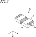
- the substantially rectangular shape of the ceramic package 2 may include a shape where the side surfaces of the container member 1 are inwardly recessed in a curved shape, so as to provide the lower surface-side of the container member 1 with external electrodes 4a connected to the discharge electrodes 4 and external electrodes 5a connected to the discharge induction electrode 5.
- wall surfaces of the curved recessed portions are provided with the external electrodes 4a and the external electrodes 5a, respectively.
- the light-emitting device 10 may be configured as a surface-mounting type having the external electrodes 4a and 5a on the lower surface of the container member 1.
- the light-emitting device 10 can enable the miniaturization, the thinning or the reduction in height and can be mounted in an electronic device, for example.
- the electronic device may be a digital camera, a portable phone having a camera, a smart phone having a camera, or the like.
- the curved recessed portion is provided as a groove shape extending from the upper surface to the lower surface of the ceramic package 2 on the side surface of the ceramic package 2, like the curved depressed portion.
- a cross-sectional shape of the recessed portion is a curved shape, for example, a semi-circular shape.
- the cross-sectional shape of the recessed portion is not limited to the semi-circular shape, and may be a half oval shape, a semi-elliptical shape or the like. That is, the shape is not particularly limited.
- the light transmitting member 3 is a light transmitting inorganic member having a substantially rectangular shape, as seen from a plan view, and is joined to upper surfaces of the sidewalls 2a of the ceramic package 2 via the joining layer 7a formed of the joining material 7 so as to close the depressed portion 2b of the ceramic package 2.
- the substantially rectangular shape of the light transmitting member 3 includes a shape where four corner portions are outwardly convex in a curved shape, so as to reduce a possibility of the damage upon assembling, for example.
- a step portion 2d may be provided over an entire circumference of the inner peripheries-side of the sidewalls 2a located at the upper surface-side of the ceramic package 2, and the light transmitting member 3 may be joined to the step portion 2d provided over the entire circumference via the joining layer 7a formed of the joining material 7 so as to close the depressed portion 2b of the ceramic package 2.
- the container member 1 has therein the hollow discharge space S formed by the ceramic package 2 and the light transmitting member 3 joined to the sidewalls 2a of the ceramic package 2 via the joining layer 7a formed of the joining material 7 so as to close the depressed portion 2b.
- the light transmitting property of the light transmitting member 3 means that a wavelength of at least part of the light emitted resulting from the light emission in the discharge space S can be transmitted.
- the light transmitting inorganic member configuring the light transmitting member 3 is formed of a substantially insulating material.
- An example of the insulating material includes glass, for example, borosilicate glass, quartz glass or the like.
- the discharge space S has a substantially rectangular shape, as seen from a plan view.
- the substantially rectangular shape of the discharge space S includes a shape where four corner portions are outwardly convex in a curved shape, so as to reduce a possibility of the damage upon assembling, for example.
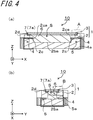
- the discharge space S of the container member 1 is defined by the depressed portion 2b, which is formed by the sidewalls 2a having the step portions 2c of the ceramic package 2, and the light transmitting member 3, in a longitudinal section.
- the inert gas 6 is encapsulated.
- the inert gas 6 is a gas containing xenon (Xe), krypton (Kr), argon (Ar), neon (Ne) and helium (He) as main components, or a mixed gas thereof.
- the couple of discharge electrodes 4 are respectively disposed so that one end portion-side (side surface 2ca-side) is disposed on the step portion 2c and a part of the upper surface is thus exposed into the discharge space S and a remaining part of the other end portion-side is disposed in the sidewall 2a of the ceramic package 2.
- the couple of discharge electrodes 4 are respectively disposed so that a tip portion thereof is flush with the side surface 2ca of the step portion 2c.
- the couple of discharge electrodes 4 may be disposed on the upper surfaces of the step portions 2c so as to be located more outwardly than the side surfaces 2ca of the step portions 2c, inasmuch as the opposite parts 4b are located more inwardly than the inner periphery of the discharge induction electrode 5.
- the couple of discharge electrodes 4 are disposed on the step portions 2c of the opposite sidewalls 2a of the ceramic package 2, and has the opposite parts 4b disposed to face each other.
- the couple of discharge electrodes 4 are provided so that the opposite parts 4b are located to face each other in the discharge space S. That is, the couple of discharge electrodes 4 are disposed on the upper surfaces of the step portions 2c of the sidewalls 2a of the ceramic package 2 so that at least parts thereof are exposed in the discharge space S so as to cause the discharge in the discharge space S.
- the discharge electrode 4 is disposed to entirely cover the upper surface of the step portion 2c. Also, the discharge electrode 4 may be disposed on the upper surface of the step portion 2c so that parts of both sides in the Y direction of the upper surface of the step portion 2c are exposed.
- the couple of discharge electrodes 4 are disposed on the upper surfaces of the step portions 2c, the discharge is difficult to occur between the discharge electrodes 4 and the bottom surface 2ba of the ceramic package 2, so that it is possible to suppress a decrease in light emission efficiency.
- the couple of discharge electrodes 4 have tip portions, which are the opposite parts 4b, and is disposed in the discharge space S so that the tip portions face each other. Also, an interval between the opposite parts 4b of the couple of discharge electrodes 4 is 3 mm to 20 mm, for example.
- the heights of the couple of opposite step portions 2c are set so that the height of one step portion 2c from the bottom surface 2ba of the step portion 2c is within a range of 65% to 135% of the height of the other step portion 2c from the bottom surface 2ba. Therefore, when the respective heights of the couple of step portions 2c in the Z direction are within the range and the couple of discharge electrodes 4 are provided at the step portions 2c, it is assumed that the couple of discharge electrodes 4 have the opposite parts 4b disposed to face each other. That is, in the Z direction, the couple of discharge electrodes 4 may be disposed so that the opposite parts 4b deviate within the range. Also, the couple of discharge electrodes 4 may deviate in the Y direction inasmuch as they have the opposite parts 4b arranged to face each other in the Z direction.
- the couple of discharge electrodes 4 are led out on the side surfaces in the longitudinal direction (X direction) of the ceramic package 2 from the inside of the discharge space S of the container member 1 to the lower surface-side of the container member 1 by the external electrodes 4a, and the discharge electrodes 4 and the external electrodes 4a are electrically and physically connected.
- the external electrode 4a also includes an electrode disposed on the lower surface of the container member 1.
- examples of a material of the external electrode 4a include tungsten, molybdenum, manganese, strontium, lanthanum, and platinum.
- one discharge electrode 4 is an anode and the other discharge electrode 4 is a cathode.
- examples of the discharge electrode 4 include high-melting-point metal including tungsten.
- examples of the material of the discharge electrode 4 include lanthanum oxide, yttrium oxide, and cerium oxide which have an excellent electron emission property, in addition to tungsten which is a main component.
- An electrode thickness of the discharge electrode 4 is 5 ⁇ m to 500 ⁇ m, for example.
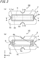
- the discharge induction electrode 5 has an annular shape, is disposed in the ceramic package 2 so as to be below the couple of discharge electrodes 4 and surround the depressed portion 2b, as seen from a plan view. Also, as shown in FIG. 2 , the discharge induction electrode 5 has an annular shape and is disposed to surround the bottom surface 2ba (bottom part) of the depressed portion 2b. When the depressed portion 2b has a V-shape, the discharge induction electrode 5 may be disposed in the ceramic package 2 so as to be below the couple of discharge electrodes 4 and surround the bottom surface 2ba (bottom part) of the depressed portion 2b or come close to the inner wall surface of the depressed portion 2b. In the meantime, the discharge induction electrode 5 is shown with the dotted line in FIG. 3(b) .
- the annular discharge induction electrode 5 is disposed in the ceramic package 2 so as to surround the bottom surface 2ba of the depressed portion 2b and not to be exposed to the discharge space S, the scattered reflection of the emitted light, which is caused due to the discharge induction electrode 5, is difficult to occur in the discharge space S of the light-emitting device 10. Also, since in the light-emitting device 10, the annular discharge induction electrode 5 is disposed in the ceramic package 2 so as to be below the couple of discharge electrodes 4 and so as not to be exposed into the discharge space S so that the light emission is not to be disturbed, the decrease in the light emission amount is suppressed.
- the discharge induction electrode 5 is disposed in the ceramic package 2 of the container member 1 so as to be below the couple of discharge electrodes 4 and so as not to be exposed into the discharge space S. That is, as shown in FIGS. 3 and 4 , since the discharge induction electrode 5 is disposed at the periphery of the sidewalls 2a in the ceramic package 2, it is possible to shorten the distance between the discharge electrode 4 and the discharge induction electrode 5 in the X direction or the Z direction. Thereby, the discharge in the discharge space S can be easily induced by the discharge induction electrode 5. Also, as shown in FIG. 3 , the couple of discharge electrodes 4 are disposed so that the opposite parts 4b are located more inwardly than the inner periphery of the annular discharge induction electrode 5, as seen from a plan view.
- a thickness of the discharge induction electrode 5 is 5 ⁇ m to 300 ⁇ m, for example, and a width thereof is 30 ⁇ m to 500 ⁇ m, for example.
- the interval between the discharge electrode 4 and the discharge induction electrode 5 in the Z direction is 25 ⁇ m to 300 ⁇ m, for example.
- the distance may be shortened so as to easily cause the discharge inasmuch as the annular discharge induction electrode 5 is not contacted with the discharge electrode 4.
- a distance between the inner peripheral surface (side surface 2ca) of the sidewall 2a of the ceramic package 2 and the inner periphery of the discharge induction electrode 5 is 10 ⁇ m to 500 ⁇ m, for example. This distance can be shortened so as to easily cause the discharge inasmuch as the annular discharge induction electrode 5 is not exposed to the inner peripheral surface of the sidewall 2a.
- the discharge induction electrode 5 is led out on each side surface in the width direction (Y direction) of the ceramic package 2 from the inside of the container member 1 to the lower surface-side of the container member 1 by the external electrodes 5a, and the discharge induction electrode 5 and the external electrodes 5a are electrically and physically connected.
- the external electrode 5a also includes an electrode provided on the lower surface of the container member 1.
- examples of a material of the external electrode 5a include tungsten, molybdenum, strontium, lanthanum, manganese, and platinum.
- examples of a material of the discharge induction electrode 5 include high-melting-point metal such as tungsten, molybdenum, strontium, lanthanum, manganese, platinum.
- the light-emitting device 10 includes the discharge induction electrode 5, so that it is possible to perform preliminary discharge. Therefore, the light-emitting device 10 can stabilize the start of the main discharge by the couple of discharge electrodes 4 and the discharge induction electrode 5.
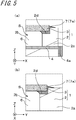
- the light transmitting member 3 is joined to the sidewalls 2a of the ceramic package 2 via the joining layer 7a formed of the joining material 7, as shown in FIGS. 3 to 5 . Also, as shown in FIGS. 3 to 5 , the step portion 2d of the light-emitting device 10 is provided over the entire circumference of the inner peripheries-side of the sidewalls 2a of the ceramic package 2, and the light transmitting member 3 is joined to the step portion 2d via the joining layer 7a formed of the joining material 7.
- the joining material 7 is composed of glass exhibiting a white color. Since the oxide ceramic powder is contained in the glass, molecules of the oxide ceramic powder exists between molecules of the glass. In particular, as a material having a favorable joining ability with the ceramic package 2 and the glass of the material of the light transmitting member 3, a low-melting-point glass can be used.
- the low-melting-point glass means glass of which a melting point is within a range of 400°C to 650°C.
- the joining material 7 is composed of a material in which alumina (aluminum oxide, Al 2 O 3 ) powder or zirconia (zirconium dioxide, ZrO 2 ) powder serving as the oxide ceramic powders is added to the low-melting-point glass containing bismuth oxide, zinc oxide or silicon oxide as a main component.
- alumina aluminum oxide, Al 2 O 3
- zirconia zirconium dioxide, ZrO 2
- the low-melting-point glass and the oxide ceramic powder having the substantially same particle diameter are mixed and pasted as powers using a triple roll. For this reason, since the oxide ceramic powder added in the low-melting-point glass is uniformly dispersed in the low-melting-point glass, the melting point of glass is little changed. Also, since the low-melting-point glass and the oxide ceramic powder is all oxides, the joining ability therebetween is good, and voids are difficult to be generated between the low-melting-point glass and the oxide ceramic powder.
- glass properties of the bismuth oxide-based low-melting-point glass such as coefficient of thermal expansion, glass-transition point and softening point can be adjusted through composition control by minor addition of zinc oxide, silicon oxide, boron oxide and alkali earth metal oxide, it is possible to design a material in conformity to a joining target.
- the joining between the ceramic package 2 and the light transmitting member 3 is performed at heating temperatures of 500°C to 700°C, for example.
- the low-melting-point glass containing bismuth oxide, zinc oxide or silicon oxide as a main component indicates glass of which the main component is 50 to 90 mass% and any one of bismuth oxide, zinc oxide, silicon oxide, boron oxide and alkali earth metal oxide is included as the remaining component.
- the oxide ceramic powder indicates a powder made of a material exhibiting a white color and having reflectance of 70% or greater in all wavelengths of the visible light region (wavelength range of 400 nm to 800 nm), for example.
- alumina, zirconia and the like may be exemplified.
- the oxide ceramic powder exhibits a white color, it is possible to increase the reflectance by adding the oxide ceramic powder to the low-melting-point glass.
- the ceramic package 2 and the light transmitting member 3 of the light-emitting device 10 are joined to each other via the joining layer 7a formed of the joining material 7, the joining layer 7a is located between the step portion 2d and the light transmitting member 3, and a part of the joining layer 7a faces toward the discharge space S.
- the joining material 7 is a material in which the alumina or zirconia powder is added to the low-melting-point glass containing bismuth oxides as a main component.
- the alumina powder is added to the low-melting-point glass including Bi 2 O 3 /SiO 2 /B 2 O 3 .
- the alumina powder or zirconia powder is added to the low-melting-point glass containing zinc oxide as a main component.
- the alumina powder or zirconia powder is added to the low-melting-point glass including ZnO/SiO 2 /B 2 O 3 /R 2 O (R: alkali metal such as lithium, sodium or potassium).
- the alumina powder or zirconia powder is added to the low-melting-point glass containing silicon oxides as a main component.
- the alumina powder is added to the low-melting-point glass including SiO 2 /RO/R 2 O (R: alkali metal such as lithium, sodium or potassium).
- the joining material 7 a material in which the low-melting-point glass exhibiting a white color contains bismuth oxides as a main component and the oxide ceramic powder is the alumina powder is described below.
- FIG. 7 illustrates a relationship between an added amount of alumina (mass%) and the reflectance and a relationship between the added amount of alumina (mass%) and a He-leak rate.
- FIG. 7 illustrates a relationship between the added amount of alumina powder (mass%) and the reflectance and a relationship between the added amount of alumina powder (mass%) and the He-leak rate when the ceramic package 2 and the light transmitting member 3 are joined by the joining material 7 in an oxygen atmosphere.
- the joining material 7 When the added amount of alumina powder is 0 mass%, the joining material 7 is formed of only the low-melting-point glass, and when the added amount of alumina powder is 100 mass%, the joining material 7 is formed of only the alumina powder. However, when the added amount of alumina powder is 100 mass%, there is no function as a joining material. Also, when the added amount of alumina powder is 40 mass%, for example, it indicates that the low-melting-point glass of the joining material 7 is 60 mass%.
- the reflectance indicates a value as to a change in the added amount of the alumina powder to the low-melting-point glass containing bismuth oxides as a main component.
- the reflectance was measured in the visible light region with a spectrophotometer by using a sample, which was manufactured by coating the low-melting-point glass having the alumina powder added thereto onto the light transmitting member 3 in a thickness of about 100 nm and applying the same thermal hysteresis as a manufacturing process of the ceramic package 2.
- the He-leak rate is obtained by a He-leak test and is to evaluate airtightness of the container member 1 resulting from the joining between the ceramic package 2 and the light transmitting member.
- the container member 1 (the ceramic package 2 and the light transmitting member 3 are joined) is first subjected to a He-pressurizing condition. Then, when there is a leak path (a part in which the airtightness is broken) in the container member 1 subjected to the He-pressurizing condition, He enters the container member 1 through the leak path. Therefore, when He entering the container member 1 is vacuumed and is effectively taken out from the container member 1, it is possible to obtain a He-leak rate from a detected amount of the He gas.
- the container member 1 includes the light transmitting member 3 which is attached to the ceramic package 2 via the joining layer 7a formed of the joining material 7, the joining layer 7a is positioned between the step portion 2d of the sidewalls 2a and the light transmitting member 3, and a part of the joining layer 7a faces toward the discharge space S. Therefore, the light resulting from the discharge between the couple of discharge electrodes 4 in the discharge space S of the container member 1 is partially incident on the joining layer 7a.
- the light incident on the joining layer 7a is partially reflected on the joining layer 7a, and the remaining light is transmitted therethrough and is diffusively reflected in the joining layer 7a, so that the light is emitted to the inside or outside of the container member 1 or is absorbed in the joining layer 7a. Therefore, the light loss is likely to occur in the joining layer 7a of the container member 1. Due to the light loss in the joining layer 7a, the light emission amount may be decreased in the light-emitting device 10.
- the ceramic package 2 and the light transmitting member 3 of the light-emitting device 10 are joined via the joining layer 7a formed of the joining material 7, and the joining material 7 includes the alumina powder added to the low-melting-point glass containing bismuth oxides as a main component. Therefore, as shown in FIG. 7 , as the added amount of alumina powder increases, the reflectance increases. For example, when the added amount of alumina powder is 10 mass%, the reflectance is 50%, which is higher than 30% which is the reflectance when the added amount of alumina powder is 0 mass% (i.e., the alumina powder is not added). The reflectance of the light-emitting device 10 is increased by adding the alumina powder to the joining material 7. However, in order to further increase the reflectance, the added amount of alumina powder to the low-melting-point glass is preferably 20 mass% or greater.
- the reflectance of the joining layer 7a increases, so that the amount of light, which is reflected into the discharge space S, of the light incident on the joining layer 7a increases. Thereby, it is possible to suppress the decrease in the light emission amount.
- the reflectance of the joining layer 7a is improved, so that the light reflected on the joining layer 7a is incident on the upper surfaces (surfaces) of the couple of discharge electrodes 4, and the incident light is reflected on the upper surfaces (surfaces) of the discharge electrodes 4, is transmitted through the light transmitting member 3 and is emitted to the outside. Therefore, the light-emitting device 10 can suppress the decrease in the light emission amount.
- the light reflected on the joining layer 7a is incident on the inner wall surface in the ceramic package 2, and the incident light is reflected on the inner wall surface, is transmitted through the light transmitting member 3 and is emitted to the outside. Therefore, the light-emitting device 10 can suppress the decrease in the light emission amount.
- the light-emitting device 10 preferably has the He-leak rate less than 1.0 ⁇ 10 -10 Pa ⁇ m 3 /sec.
- "1.0 ⁇ 10 -10 " is denoted as "1.0E-10". Therefore, in the light-emitting device 10, the added amount of alumina powder to the low-melting-point glass is preferably 40 mass% or less. In the meantime, from standpoints of the joining property or the airtightness, the added amount of alumina powder is preferably less than 50 mass%.
- the added amount of alumina powder to the low-melting-point glass can be set to 20 to 40 mass%, considering the compatibility of the reflectance and the airtightness.
- FIG. 8 illustrates a relationship between the added amount of alumina powder (mass%) and the reflectance and a relationship between the added amount of alumina powder (mass%) and the He-leak rate when the ceramic package 2 and the light transmitting member 3 are joined by the joining material 7 in a non-oxygen atmosphere.
- FIG. 8 illustrates a relationship between the added amount of alumina powder and the reflectance and a relationship between the added amount of alumina powder and the He-leak rate when the ceramic package 2 and the light transmitting member 3 of the light-emitting device 10 are joined via the joining layer 7a formed of the joining material 7 in the non-oxygen atmosphere.
- the non-oxygen atmosphere is a nitrogen atmosphere.
- a high-melting-point metal material such as tungsten, molybdenum or the like is used so as to endure the heat upon the discharge.
- the high-melting-point metal material is susceptible to oxidation.
- tungsten is used for the couple of discharge electrodes 4, for example, if the ceramic package 2 and the light transmitting member 3 are joined via the joining layer 7a formed of the joining material 7 in the oxygen atmosphere, the joining layer 7a is oxidized, so that the function as the discharge electrode is degraded and the discharge efficiency is likely to be lowered. Also, as the discharge electrode 4 is oxidized, the discharge does not occur. Therefore, when an easily-oxidizable metal material is used for the couple of discharge electrodes 4, the ceramic package 2 and the light transmitting member 3 are joined in the non-oxygen atmosphere so as to suppress the oxidation of the couple of discharge electrodes 4.
- the joining between the ceramic package 2 and the light transmitting member 3 is performed in the non-oxygen atmosphere.
- the non-oxygen atmosphere is not limited to the nitrogen atmosphere.
- the joining between the ceramic package 2 and the light transmitting member 3 in the non-oxygen atmosphere may be performed in vacuum or forming gas (mixed gas of hydrogen and ammonia) or in a reducing atmosphere.
- the vacuum the bismuth oxide is dissociated (reduced) by heating and is likely to be a metal state from a suboxidation state.
- the bismuth oxide is likely to be a metal state from a suboxidation state due to a reduction action of the hydrogen gas.
- the reflectance is 10%.
- the reason is as follows. That is, when the ceramic package 2 and the light transmitting member 3 are joined to each other via the joining layer 7a formed of the joining material 7 in the nitrogen atmosphere, the oxygen of the bismuth oxide is lost by the reducing property of nitrogen in the atmosphere, so that the bismuth oxide is likely to be a suboxidation state.
- the joining material 7 is likely to be a color of a metal component of bismuth and is blackened, so that the reflectance is lower, as compared to the case where the joining is performed in the oxygen atmosphere. Therefore, the reflectance is lower than 30% which is the reflectance when the added amount of alumina powder is 0 mass% in the oxygen atmosphere.
- the added alumina powder supplies the oxygen to the bismuth oxides at the suboxidation state.
- the bismuth oxide at the suboxidation state is supplied with the oxygen from the alumina powder, so that the oxidation proceeds and thereby the original white color of the bismuth oxide can be kept. Therefore, it is possible to suppress the decrease in the reflectance. Also, it is possible to increase the reflectance by adding the alumina powder exhibiting a white color.
- the joining material 7 is obtained by adding the alumina powder to the low-melting-point glass containing bismuth oxides as a main component, and the reflectance thereof increases as the added amount of alumina powder to the low-melting-point glass increases, as shown in FIG. 8 .
- the added amount of the alumina powder is 10%
- the reflectance is 25%, which is higher than 10% which is the reflectance when the added amount of alumina powder is 0 mass%, i.e., the alumina powder are not added.
- the reflectance is increased and the oxygen is supplied to the bismuth oxides at the suboxidation state, so that the bismuth oxides are suppressed from being the suboxidation state.
- the reflectance is increased and the oxygen is supplied to the bismuth oxides at the suboxidation state, so that the bismuth oxides are suppressed from being the suboxidation state.
- the reflectance of the light-emitting device 10 is increased by adding the alumina powder.
- the added amount of alumina powder to the low-melting-point glass may be set to 20 mass% or greater.
- the reflectance of the joining layer 7a is improved, so that the amount of light, which is reflected into the discharge space S, of the light incident on the joining layer 7a increases. Thereby, it is possible to suppress the decrease in the light emission amount.
- the reflectance of the joining layer 7a is improved, so that the light reflected on the joining layer 7a is incident on the upper surfaces (surfaces) of the couple of discharge electrodes 4 and the incident light is reflected on the upper surfaces (surfaces) of the discharge electrodes 4, is transmitted through the light transmitting member 3 and is emitted to the outside. Thereby, it is possible to suppress the decrease in the light emission amount.
- the light reflected on the joining layer 7a is incident on the inner wall surface in the ceramic package 2 and the incident light is reflected on the inner wall surface, is transmitted through the light transmitting member 3 and is emitted to the outside, so that the light-emitting device 10 can suppress the decrease in the light emission amount.
- the He-leak rate may be less than 1.0 ⁇ 10 -10 Pa ⁇ m 3 /sec.
- "1.0 ⁇ 10 -10” is denoted as "1.0E-10". Therefore, in the light-emitting device 10, the added amount of alumina powder to the low-melting-point glass may be 40 mass% or less.
- the added amount of alumina powder to the low-melting-point glass may be set to 20 mass% to 40 mass%, considering the compatibility of the reflectance and the airtightness.
- FIG. 9 illustrates a relation between the added amount of alumina powder (mass%) and a light emission amount ratio (%).
- the added amount of alumina powder of the joining material 7 is 0 mass%, the joining material is made of only the low-melting-point glass, and when the added amount of alumina powder is 100 mass%, the joining material is made of only the alumina powder.
- the added amount of alumina powder is 100 mass%, there is no function as a joining material.
- the added amount of alumina powder is 40 mass%, for example, it indicates that the low-melting-point glass of the joining material 7 is 60 mass%.
- the light emission amount ratio shown in FIG. 9 indicates a light emission amount ratio when the added amount of alumina powder is increased, on the basis of the added amount of alumina powder of 0 mass%. It can be seen that when the added amount of alumina powder to the low-melting-point glass is increased, the light emission amount of the light-emitting device is improved until the added amount of alumina powder becomes 40 mass%. When the added amount of alumina powder is further increased, the amount of the low-melting-point glass in the joining material 7 is reduced, so that the measurement could not be made due to the airtightness defect caused in the light-emitting device. In the meantime, the light emission amount was measured using a measurement device CM-A148 available from Konica Minolta, Inc., the measurement wavelength region was 360 nm to 740 nm, and the light emission amount was measured by total luminous flux measurement.
- CM-A148 available from Konica Minolta, Inc.
- the ceramic package 2 is composed of a plurality of insulating layers which are laminated one another.
- the insulating layer is formed of an electrically insulating material such as aluminum oxide sintered body, aluminum nitride sintered body, silicon carbide sintered body, silicon nitride sintered body, mullite sintered body or ceramic material such as glass ceramics, for example.
- the ceramic package 2 is formed by laminating a plurality of ceramic green sheets by using a ceramic green sheet lamination method, for example.
- the ceramic package 2 is formed of aluminum oxide sintered body, for example, appropriate organic binder, solvent and the like are first added to and mixed with raw material powder such as aluminum oxide, silicon oxide, calcium oxide or magnesium oxide, so that a slurry is formed. Then, the slurry is formed into a sheet shape by a sheet forming method such as a doctor blade method, so that a ceramic green sheet becoming the insulating layer is obtained.
- raw material powder such as aluminum oxide, silicon oxide, calcium oxide or magnesium oxide
- a paste layer becoming the couple of discharge electrodes 4 and the discharge induction electrode 5 is formed by applying screen printing or otherwise to the ceramic green sheet, depending on the configurations of the couple of discharge electrodes 4, the discharge induction electrode 5 and the like of the ceramic package 2. Also, in the same manner, a paste layer becoming the external electrodes 4a and the external electrodes 5a of the lower surface of the ceramic package 2 is formed by applying the screen printing or otherwise to the ceramic green sheet.
- a paste layer becoming the external electrodes 4a and the external electrodes 5a is formed by applying the screen printing or otherwise to the ceramic green sheet, in the same manner. Then, a plurality of punched ceramic green sheets is laminated at positions of the external electrodes 4a and the external electrodes 5a by using a ceramic green sheet lamination method or otherwise.
- the ceramic green sheet is formed with a through-hole becoming the depressed portion 2b by a hole forming method using a punching mold or the like.
- the metal material such as tungsten(W), molybdenum(Mo), molybdenum-manganese(Mo-Mn), copper(Cu), silver (Ag) or silver-palladium(Ag-Pd) can be used for each electrode.
- a conductive paste becoming the electrode is obtained by adding and mixing the appropriate organic binder, solvent and the like with powder of tungsten(W), molybdenum(Mo), molybdenum-manganese(Mo-Mn), copper(Cu), silver (Ag) or silver-palladium (Ag-Pd) .
- the conductive paste is beforehand applied by printing in a predetermined pattern on the ceramic green sheet becoming the ceramic package 2 by using the screen printing method, so that a paste layer is formed.
- the firing is performed at the same time with the plurality of laminated ceramic green sheets becoming the ceramic package 2, so that the couple of discharge electrodes 4, the discharge induction electrode 5, the external electrodes 4a and the external electrodes 5a are formed at predetermined positions of the ceramic package 2.
- the ceramic green sheet is cut into an appropriate size and the plurality of ceramic green sheets is laminated to constitute the ceramic package 2, so that a stacked body is manufactured. Thereafter, the stacked body is fired at temperatures of about 1600°C in the reducing atmosphere, so that the ceramic package 2 having the plurality of insulating layers laminated is manufactured. Also, the reducing atmosphere is a nitrogen atmosphere, for example.
- the ceramic package 2 is provided with the couple of discharge electrodes 4 and the discharge induction electrode 5, the side surfaces and the lower surface thereof are provided with the external electrodes 4a connected to the discharge electrode 4 and the external electrodes 5a connected to the discharge induction electrode 5.
- the light transmitting member 3 is joined to the ceramic package 2 via the joining layer 7a formed of the joining material 7 so as to close the depressed portion 2b.
- the glass paste obtained by adding and mixing the appropriate binder, solvent and the like to the low-melting-point glass having the alumina powder added thereto
- the joining material 7 is applied to the sidewall 2a or the joining region of the light transmitting member 3 by using the screen printing method, in conformity to the shape of the joining region between the ceramic package 2 and the light transmitting member 3.
- the light transmitting member 3 is placed on the step portion 2d of the sidewalls 2a of the ceramic package 2 by using an alignment jig conforming to the shape of the light transmitting member 3 or the ceramic package 2, and a binder removing process of removing the solvent or binder component included in the joining material 7 is performed at heating temperatures of 200°C to 300°C, for example. Then, the ceramic package 2 and the light transmitting member 3 are joined to each other at heating temperatures of 500°C to 700°C, for example. By this process, it is possible to obtain the container member 1.
- the discharge electrode 4 is formed of an easily-oxidizable metal material such as tungsten, for example, it is difficult to be oxidized at heating temperatures of 200°C to 300°C.
- the joining is performed by the same method as the joining in the oxygen atmosphere.
- the binder removing process of removing the solvent or binder component included in the glass paste serving as the joining material 7 at heating temperatures of 200°C to 300°C may also be performed in the oxygen atmosphere.
- the ceramic package 2 is provided with a gas introduction hole (not shown) for introducing the inert gas 6 into the container member 1, and the inert gas 6 (Xe gas) is introduced into the container member 1 through the gas introduction hole.
- the gas introduction hole is sealed after introduction of the inert gas 6.
- the joining material 7 is obtained by mixing the low-melting-point glass containing powder of bismuth oxide as a main component and alumina powder with the appropriate solvent or binder while pulverizing the powder by a mortar and then dispersing the same by using a triple roll or otherwise.
- the low-melting-point glass containing bismuth oxides as a main component is powder whose particle diameter is 0.5 ⁇ m to 10 ⁇ m, and the alumina powder has a particle diameter of 0.2 ⁇ m to 10 ⁇ m, for example.
- the invention is not limited to the light-emitting device 10 of the above embodiment and various changes or modifications are possible without departing from the scope of the invention.
- other embodiments of the invention are described.
- the same parts as the light-emitting device 10 of the above embodiment are denoted by the same reference numerals, and the descriptions thereof are appropriately omitted.
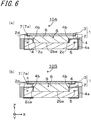
- a light-emitting device 10A may have a configuration where the couple of discharge electrodes 4 extends downward (toward the bottom surface 2ba) along the inner peripheral surfaces of the sidewalls 2a.
- the parts, which extend downward and are provided on the inner peripheral surfaces, of the couple of discharge electrodes 4 are the opposite parts 4b.
- the couple of discharge electrodes 4 are exposed to the discharge space S, and the discharge is caused from one exposed discharge electrode 4 with respect to the other opposite discharge electrode 4 at a part at which a distance between electrodes is shortest, in the inert gas 6 (Xe).
- the discharge electrode 4 is worn and rounded at a locally discharged part thereof, and in a next discharge, the discharge is caused from a separate place of the one discharge electrode 4 with respect to the other discharge electrode 4.
- a light-emitting device 10B may have a configuration where the couple of discharge electrodes 4 are disposed on the sidewalls 2a of the ceramic package 2 so as to reach the inner peripheral surfaces from the inside of the sidewalls 2a and extends downward (toward the bottom surface 2ba) from the part reaching the inner peripheral surfaces along the inner peripheral surfaces (side surfaces 2ca) of the sidewalls 2a.
- the parts provided on the inner peripheral surfaces (side surfaces 2ca) of the couple of sidewalls 2a are the opposite parts 4b of the discharge electrodes 4.
Landscapes
- Engineering & Computer Science (AREA)
- Manufacturing & Machinery (AREA)
- Led Device Packages (AREA)
- Vessels And Coating Films For Discharge Lamps (AREA)
- Discharge Lamps And Accessories Thereof (AREA)
Abstract
Description
- The present invention relates to a light-emitting device such for example as an electric-discharge lamp.
- In the related art, a light-emitting device such for example as an electric-discharge lamp having a structure in which an inert gas is filled in a glass tube has been known. In the light-emitting device of the related art, a couple of discharge electrodes are fixed to the glass tube with protruding from an end portion of the glass tube into a discharge space, and a discharge induction electrode is disposed on an outer periphery of the glass tube. An example of the electric-discharge lamp is disclosed in Japanese Unexamined Patent Publication
JP-A 09-180677 (1997) - In recent years, for example, the light-emitting device such as an electric-discharge lamp is needed to be further miniaturized so as to mount the same to a portable terminal and the like. However, the light-emitting device having the conventional glass tube has a structure that is difficult to be made small. In order to solve the miniaturization problem, a structure of a light-emitting device which includes a package and a light transmitting member joined to the package and has a discharge space in a container member has been known. An example of the light-emitting device is disclosed in Japanese Unexamined Patent Publication
JP-A 2011-96562 - The light-emitting device including the package and the light transmitting member joined to the package has a problem that a light emission amount decreases because the package and the light transmitting member are joined via a joining material and the light generated in the discharge space is thus likely to be absorbed by the joining material.
- The invention has been made in view of the above problems, and an object thereof is to provide a light-emitting device capable of suppressing a decrease in a light emission amount due to a joining material for joining a package and a light transmitting member.
- A light-emitting device according to an embodiment of the invention includes a container member including a ceramic package provided with a depressed portion serving as a discharge space, and a light transmitting inorganic member which is attached to the ceramic package via a joining layer formed of a joining material so as to close the depressed portion; an inert gas encapsulated inside the discharge space; and a couple of discharge electrodes which are disposed in the depressed portion of the ceramic package so as to be spaced from each other, the joining material including glass exhibiting a white color, and oxide ceramic powder.
-
-
FIG. 1(a) is an exploded perspective view illustrating a light-emitting device except a joining material according to one embodiment of the invention, andFIG. 1(b) is an exploded perspective view of a ceramic package for explaining a discharge induction electrode of the light-emitting device shown inFIG 1(a) ; -
FIG. 2 is a perspective view illustrating a state of a lower surface-side of the light-emitting device shown inFIG. 1 ; -
FIG. 3(a) is a plan view illustrating the light-emitting device according to one embodiment of the invention, andFIG. 3(b) is a plan view illustrating the light-emitting device except a light transmitting member and the joining material; -
FIG. 4(a) is a sectional view taken along the line A-A inFIG. 3(a) , andFIG. 4(b) is a sectional view taken along the line B-B inFIG. 3(a) ; -
FIG. 5(a) is an enlarged view illustrating a part indicated by reference sign A inFIG. 4(a) , andFIG. 5(b) is an enlarged view illustrating a part indicated by reference sign B inFIG. 4(b) ; -
FIGS. 6(a) and 6(b) are another examples of the light-emitting device according to another embodiment of the invention, respectively, and are sectional views taken along the line A-A inFIG. 3(a) ; -
FIG. 7 is a graph illustrating a relationship between an added amount of alumina and reflectance and a relationship between the added amount of alumina and a He-leak rate in an oxygen atmosphere; -
FIG. 8 is a graph illustrating a relationship between an added amount of alumina and reflectance and a relationship between the added amount of alumina and a He-leak rate in a non-oxygen atmosphere; and -
FIG. 9 is a graph illustrating a relationship between the added amount of alumina and a light emission amount in the non-oxygen atmosphere. - Hereinafter, a light-emitting device according to one embodiment of the invention will be described with reference to the accompanying drawings. Also, for convenience of descriptions, while defining a Cartesian coordination system XYZ and also defining a positive-side of the Z direction as upper, terms of an upper surface (surface) or a lower surface are appropriately used for the light-emitting device.
- Also, in the descriptions of the embodiment and the like, the configurations, which are the same or similar as or to the described configurations, are denoted with the same reference numerals, and the descriptions thereof may be omitted.
- A light-
emitting device 10 according to an embodiment of the invention is described with reference toFIGS. 1 to 5 . The light-emittingdevice 10 is embedded in a portable terminal such as a smart phone or an imaging device such as a digital camera. The light-emittingdevice 10 can instantaneously generate a flash light in a larger amount of light by using a discharge action of a rare gas, for example, as compared to an LED. - The light-
emitting device 10 according to one embodiment of the invention has a configuration as shown inFIGS. 1 to 5 , and includes acontainer member 1, aninert gas 6, and a couple ofdischarge electrodes 4. Thecontainer member 1 includes aceramic package 2 provided with adepressed portion 2b serving as a discharge space and a light transmittingmember 3, which is a light transmitting inorganic member which is joined to theceramic package 2 via a joininglayer 7a formed of a joiningmaterial 7 so as to close thedepressed portion 2b. Also, the couple ofdischarge electrodes 4 are disposed onopposite sidewalls 2a of theceramic package 2 and hasopposite parts 4b disposed to face each other. The joiningmaterial 7 comprises glass exhibiting a white color and oxide ceramic powder. Also, a light emission direction of the light-emitting device 10 is a positive side of the Z direction. - Also, the light-
emitting device 10 may have adischarge induction electrode 5 in theceramic package 2 so as to easily start the discharge in the discharge space S. The light-emitting device 10 is configured so that the annulardischarge induction electrode 5 is disposed in theceramic package 2 so as to be below the couple ofdischarge electrodes 4 and surround thedepressed portion 2b. Also, theopposite parts 4b of the couple ofdischarge electrodes 4 are positioned more inwardly than an inner periphery of thedischarge induction electrode 5, as seen from a plan view. - By the above configuration, the light-
emitting device 10 can be made smaller and easily generate the discharge between the couple ofdischarge electrodes 4. Also, since thecontainer member 1 can sufficiently secure the discharge space S inside theceramic package 2 and electrode areas of thedischarge electrodes 4 can be made great, the light-emittingdevice 10 can effectively generate the discharge between the couple ofdischarge electrodes 4. - Also, the light-
emitting device 10 has the annulardischarge induction electrode 5, so that it is possible to ionize the entireinert gas 6, and particularly, to ionize theinert gas 6 in the vicinity of thedischarge electrodes 4. Therefore, the discharge is likely to occur between the couple ofdischarge electrodes 4. In this way, according to the light-emitting device 10, thedischarge induction electrode 5 can facilitate the start of the discharge and the couple ofdischarge electrodes 4 can effectively cause the discharge. - The light-emitting
device 10 is an electric-discharge lamp, and is configured to use light emission by theinert gas 6 between the couple ofdischarge electrodes 4. Also, thecontainer member 1 including theceramic package 2 and thelight transmitting member 3 joined to thesidewalls 2a of theceramic package 2, the couple ofopposite discharge electrodes 4 and thedischarge induction electrode 5 constitute a light emission tube (discharge tube). For example, a portable terminal device such as a smart phone has a camera function so as to image a photographic subject, and also has an illumination light source, which is to be used upon imaging at a dark place such as night. The light-emitting device 10 is configured to generate a flash light by discharging the light emission tube (discharge tube), and can be used for a portable terminal device such as a smart phone. Also, the utility of the light-emittingdevice 10 is not limited to the illumination light source. For example, the light-emitting device can be used for a utility such as rapid heating where the high-output energy is required in a short time. - The
container member 1 includes theceramic package 2 and thelight transmitting member 3 which is attached to thesidewalls 2a of theceramic package 2 via the joininglayer 7a formed of the joiningmaterial 7. Thecontainer member 1 has therein the discharge space S, and the discharge space S is defined by theceramic package 2 and thelight transmitting member 3. - Also, the
discharge electrodes 4 are electrodes used for causing an insulation breakdown in a gas by a potential difference and enabling a current to flow through the gas, and include a couple of an anode and a cathode. Also, the discharge induction electrode is an electrode provided separately from thedischarge electrodes 4 so as to start the discharge in the discharge space, and is configured to ionize the gas (inert gas) between the couple ofdischarge electrodes 4, thereby facilitating the start of the discharge. In the meantime, thedischarge induction electrode 5 is also referred to as a trigger electrode. - As shown in
FIGS. 1 to 5 , the light-emitting device 10 has a configuration where theceramic package 2 has a couple ofstep portions 2c formed at theopposite sidewalls 2a and the couple ofdischarge electrodes 4 is disposed on the couple ofstep portions 2c. Also, the light-emitting device 10 has a length in a longitudinal direction (X direction) of 3.2 mm to 50 mm, for example, a length in a width direction (Y direction) of 1.2 mm to 30 mm, for example, and a height of 0.3 mm to 5 mm, for example, has a configuration as shown inFIGS. 1 to 5 , and enables the miniaturization, the thinning or the reduction in height. - There is described the configuration where the
ceramic package 2 of thecontainer member 1 has the couple ofstep portions 2c at theopposite sidewalls 2a and the couple ofdischarge electrodes 4 is disposed on the couple ofstep portions 2c. In the meantime, as described later, in the light-emitting device 10, the couple ofdischarge electrodes 4 is preferably disposed so that parts thereof are exposed to the discharge space S and the discharge can be thus generated between the couple ofdischarge electrodes 4. - As shown in
FIG. 1 , theceramic package 2 has thedepressed portion 2b surrounded by thesidewalls 2a and serving as the discharge space S. A shape of thedepressed portion 2b is not limited to a rectangular shape as shown inFIG. 4(b) , as seen from a cross-sectional view. For example, the depressed portion may have any sectional shape inasmuch as the light emission resulting from the discharge is to be generated in thedepressed portion 2b serving as the discharge space S. That is, the shape of thedepressed portion 2b may be a V-shape or a shape of which a width of an opening gradually decreases from an upper side of theceramic package 2 toward a lower side thereof, as seen from a cross-sectional view. - The
container member 1 has thestep portions 2c provided at theopposite sidewalls 2a (thesidewalls 2a facing each other in the X direction) so as to provide the couple ofdischarge electrodes 4 at theceramic package 2, and thestep portions 2c are configured as the couple ofstep portions 2c. That is, in theceramic package 2, a region including a central part is surrounded by the fourperipheral sidewalls 2a and thedepressed portion 2b is thus formed. Also, the couple ofstep portions 2c is disposed on inner peripheries-side of the couple ofsidewalls 2a facing each other in the longitudinal direction (X direction), and the couple ofdischarge electrodes 4 is disposed on the couple ofstep portions 2c. In this way, thecontainer member 1 has the couple ofdischarge electrodes 4 disposed on the couple ofstep portions 2c in the longitudinal direction (X direction), so that it is possible to cause the discharge in the longitudinal direction (X direction) of the discharge space S and to excite the moreinert gas 6. As a result, it is possible to improve the light emission efficiency. - Also, the
container member 1 may have the couple ofstep portions 2c at thesidewalls 2a facing each other in the width direction (Y direction) (thesidewalls 2a facing each other in the Y direction) so as to provide theceramic package 2 with the couple ofdischarge electrodes 4. Thecontainer member 1 has the couple ofdischarge electrodes 4 in the width direction (Y direction), so that a distance between the couple ofdischarge electrodes 4 becomes shorter. Thereby, the discharge is more likely to be generated in the discharge space S. - As shown in
FIG. 4 , thedischarge electrode 4 is disposed on thestep portion 2c, and an upper surface of thestep portion 2c is substantially parallel with a bottom surface 2ba (X axis) of thedepressed portion 2b, as seen from a cross-sectional view. The description "substantially parallel" means that an angle between the upper surface of thestep portion 2c and the bottom surface 2ba (X axis) of thedepressed portion 2b is within a range of 0° to ±5°. In the meantime, theangle 0° indicates that the upper surface of thestep portion 2c and the bottom surface 2ba are parallel with each other. - Also, the upper surface of the
step portion 2c may be inclined toward the bottom surface 2ba of thedepressed portion 2b. That is, the upper surface of thestep portion 2c may be inclined relative to the bottom surface 2ba (X axis) of thedepressed portion 2b within a range of 10° to 60°. The couple ofdischarge electrodes 4 is provided on the inclined upper surfaces of thestep portions 2c, so that the opposite areas of the couple ofdischarge electrodes 4 increase although it is pseudo. When the opposite areas of the couple ofdischarge electrodes 4 increase, it is possible to suppress a decrease in the lifetime of the electrodes. - Also, the couple of
step portions 2c are provided on the inner peripheries-side of thesidewalls 2a of theceramic package 2 so that heights thereof from the bottom surface 2ba of thedepressed portion 2b are substantially equal. The heights of the couple ofstep portions 2c from the bottom surface 2ba (heights of side surfaces 2ca) are 10 µm to 500 µm, for example. Also, the description "substantially equal" means that the height of onestep portion 2c from the bottom surface 2ba is within a range of 65% to 135% of the height of theother step portion 2c from the bottom surface 2ba. - Also, the
ceramic package 2 is made of a substantially insulating material and has a substantially rectangular shape, as seen from a plan view. As the insulating material of theceramic package 2, a ceramic material or a resin material such as an epoxy resin, a polyester resin or the like may be exemplified. Also, theceramic package 2 is formed of an insulating material exhibiting a white color, as the ceramic material. Theceramic package 2 may be formed of a material exhibiting a white color and having reflectance of 70% or greater in all wavelengths of a visible light region (a wavelength range of about 400 nm to 800 nm) so as to effectively reflect the light resulting from the discharge on an inner wall surface of thedepressed portion 2b of theceramic package 2. As the material, aluminum oxide sintered body (alumina ceramics), low-temperature co-fired ceramics and the like may be exemplified. Theceramic package 2 exhibits a white color, so that it is possible to increase the reflectance of the inner wall surface of thedepressed portion 2b of theceramic package 2. Therefore, it is possible to suppress a decrease in a light emission amount. Also, thecontainer member 1 includes theceramic package 2 made of ceramics, so that the durability in use is improved. - As shown in
FIGS. 1 and2 , the substantially rectangular shape of theceramic package 2 includes a shape where four corner portions of theceramic package 2 are inwardly depressed and a shape where the four corner portions have C-chamfered or R-chamfered structure, so as to reduce a possibility of the damage upon conveyance or upon mounting. Also, the description "as seen from a plan view" indicates a line of sight from above toward a negative direction of the Z axis, inFIG. 1 . The curved depressed portion is provided as a groove shape extending from an upper surface to a lower surface of theceramic package 2 at the corner portion of theceramic package 2. A cross-sectional shape of the depressed portion is a curved shape. - Also, as shown in
FIGS. 1 and2 , the substantially rectangular shape of theceramic package 2 may include a shape where the side surfaces of thecontainer member 1 are inwardly recessed in a curved shape, so as to provide the lower surface-side of thecontainer member 1 withexternal electrodes 4a connected to thedischarge electrodes 4 andexternal electrodes 5a connected to thedischarge induction electrode 5. In this case, wall surfaces of the curved recessed portions are provided with theexternal electrodes 4a and theexternal electrodes 5a, respectively. Also, the light-emittingdevice 10 may be configured as a surface-mounting type having theexternal electrodes container member 1. The light-emittingdevice 10 can enable the miniaturization, the thinning or the reduction in height and can be mounted in an electronic device, for example. The electronic device may be a digital camera, a portable phone having a camera, a smart phone having a camera, or the like. - Also, the curved recessed portion is provided as a groove shape extending from the upper surface to the lower surface of the
ceramic package 2 on the side surface of theceramic package 2, like the curved depressed portion. A cross-sectional shape of the recessed portion is a curved shape, for example, a semi-circular shape. In the meantime, the cross-sectional shape of the recessed portion is not limited to the semi-circular shape, and may be a half oval shape, a semi-elliptical shape or the like. That is, the shape is not particularly limited. - The
light transmitting member 3 is a light transmitting inorganic member having a substantially rectangular shape, as seen from a plan view, and is joined to upper surfaces of thesidewalls 2a of theceramic package 2 via the joininglayer 7a formed of the joiningmaterial 7 so as to close thedepressed portion 2b of theceramic package 2. The substantially rectangular shape of thelight transmitting member 3 includes a shape where four corner portions are outwardly convex in a curved shape, so as to reduce a possibility of the damage upon assembling, for example. - Also, in the light-emitting
device 10, as shown inFIGS. 3 to 5 , astep portion 2d may be provided over an entire circumference of the inner peripheries-side of thesidewalls 2a located at the upper surface-side of theceramic package 2, and thelight transmitting member 3 may be joined to thestep portion 2d provided over the entire circumference via the joininglayer 7a formed of the joiningmaterial 7 so as to close thedepressed portion 2b of theceramic package 2. Also in this case, thecontainer member 1 has therein the hollow discharge space S formed by theceramic package 2 and thelight transmitting member 3 joined to thesidewalls 2a of theceramic package 2 via the joininglayer 7a formed of the joiningmaterial 7 so as to close thedepressed portion 2b. - Herein, the light transmitting property of the
light transmitting member 3 means that a wavelength of at least part of the light emitted resulting from the light emission in the discharge space S can be transmitted. The light transmitting inorganic member configuring thelight transmitting member 3 is formed of a substantially insulating material. An example of the insulating material includes glass, for example, borosilicate glass, quartz glass or the like. In the meantime, the joining between theceramic package 2 and thelight transmitting member 3 via the joininglayer 7a formed of the joiningmaterial 7 will be described in detail later. - The discharge space S has a substantially rectangular shape, as seen from a plan view. The substantially rectangular shape of the discharge space S includes a shape where four corner portions are outwardly convex in a curved shape, so as to reduce a possibility of the damage upon assembling, for example. Also, the discharge space S of the
container member 1 is defined by thedepressed portion 2b, which is formed by thesidewalls 2a having thestep portions 2c of theceramic package 2, and thelight transmitting member 3, in a longitudinal section. - In the discharge space S, the
inert gas 6 is encapsulated. Theinert gas 6 is a gas containing xenon (Xe), krypton (Kr), argon (Ar), neon (Ne) and helium (He) as main components, or a mixed gas thereof. - As shown in
FIG. 3 , the couple ofdischarge electrodes 4 are respectively disposed so that one end portion-side (side surface 2ca-side) is disposed on thestep portion 2c and a part of the upper surface is thus exposed into the discharge space S and a remaining part of the other end portion-side is disposed in thesidewall 2a of theceramic package 2. InFIG. 4 , the couple ofdischarge electrodes 4 are respectively disposed so that a tip portion thereof is flush with the side surface 2ca of thestep portion 2c. Also, the couple ofdischarge electrodes 4 may be disposed on the upper surfaces of thestep portions 2c so as to be located more outwardly than the side surfaces 2ca of thestep portions 2c, inasmuch as theopposite parts 4b are located more inwardly than the inner periphery of thedischarge induction electrode 5. - As shown in
FIG. 3 , the couple ofdischarge electrodes 4 are disposed on thestep portions 2c of theopposite sidewalls 2a of theceramic package 2, and has theopposite parts 4b disposed to face each other. In this way, the couple ofdischarge electrodes 4 are provided so that theopposite parts 4b are located to face each other in the discharge space S. That is, the couple ofdischarge electrodes 4 are disposed on the upper surfaces of thestep portions 2c of thesidewalls 2a of theceramic package 2 so that at least parts thereof are exposed in the discharge space S so as to cause the discharge in the discharge space S. - Also, as shown in
FIG. 4 , thedischarge electrode 4 is disposed to entirely cover the upper surface of thestep portion 2c. Also, thedischarge electrode 4 may be disposed on the upper surface of thestep portion 2c so that parts of both sides in the Y direction of the upper surface of thestep portion 2c are exposed. - Since the couple of
discharge electrodes 4 are disposed on the upper surfaces of thestep portions 2c, the discharge is difficult to occur between thedischarge electrodes 4 and the bottom surface 2ba of theceramic package 2, so that it is possible to suppress a decrease in light emission efficiency. - Also, as shown in
FIG. 3 , the couple ofdischarge electrodes 4 have tip portions, which are theopposite parts 4b, and is disposed in the discharge space S so that the tip portions face each other. Also, an interval between theopposite parts 4b of the couple ofdischarge electrodes 4 is 3 mm to 20 mm, for example. - Also, the heights of the couple of
opposite step portions 2c (heights of the side surfaces 2ca) are set so that the height of onestep portion 2c from the bottom surface 2ba of thestep portion 2c is within a range of 65% to 135% of the height of theother step portion 2c from the bottom surface 2ba. Therefore, when the respective heights of the couple ofstep portions 2c in the Z direction are within the range and the couple ofdischarge electrodes 4 are provided at thestep portions 2c, it is assumed that the couple ofdischarge electrodes 4 have theopposite parts 4b disposed to face each other. That is, in the Z direction, the couple ofdischarge electrodes 4 may be disposed so that theopposite parts 4b deviate within the range. Also, the couple ofdischarge electrodes 4 may deviate in the Y direction inasmuch as they have theopposite parts 4b arranged to face each other in the Z direction. - As shown in
FIGS. 1 to 3 , the couple ofdischarge electrodes 4 are led out on the side surfaces in the longitudinal direction (X direction) of theceramic package 2 from the inside of the discharge space S of thecontainer member 1 to the lower surface-side of thecontainer member 1 by theexternal electrodes 4a, and thedischarge electrodes 4 and theexternal electrodes 4a are electrically and physically connected. In the meantime, theexternal electrode 4a also includes an electrode disposed on the lower surface of thecontainer member 1. Also, examples of a material of theexternal electrode 4a include tungsten, molybdenum, manganese, strontium, lanthanum, and platinum. - Also, of the couple of
discharge electrodes 4, onedischarge electrode 4 is an anode and theother discharge electrode 4 is a cathode. When thedischarge electrode 4 is an anode, examples of thedischarge electrode 4 include high-melting-point metal including tungsten. Also, when thedischarge electrode 4 is a cathode, examples of the material of thedischarge electrode 4 include lanthanum oxide, yttrium oxide, and cerium oxide which have an excellent electron emission property, in addition to tungsten which is a main component. An electrode thickness of thedischarge electrode 4 is 5 µm to 500 µm, for example. - As shown in
FIG. 3 , thedischarge induction electrode 5 has an annular shape, is disposed in theceramic package 2 so as to be below the couple ofdischarge electrodes 4 and surround thedepressed portion 2b, as seen from a plan view. Also, as shown inFIG. 2 , thedischarge induction electrode 5 has an annular shape and is disposed to surround the bottom surface 2ba (bottom part) of thedepressed portion 2b. When thedepressed portion 2b has a V-shape, thedischarge induction electrode 5 may be disposed in theceramic package 2 so as to be below the couple ofdischarge electrodes 4 and surround the bottom surface 2ba (bottom part) of thedepressed portion 2b or come close to the inner wall surface of thedepressed portion 2b. In the meantime, thedischarge induction electrode 5 is shown with the dotted line inFIG. 3(b) . - In this way, since the annular
discharge induction electrode 5 is disposed in theceramic package 2 so as to surround the bottom surface 2ba of thedepressed portion 2b and not to be exposed to the discharge space S, the scattered reflection of the emitted light, which is caused due to thedischarge induction electrode 5, is difficult to occur in the discharge space S of the light-emittingdevice 10. Also, since in the light-emittingdevice 10, the annulardischarge induction electrode 5 is disposed in theceramic package 2 so as to be below the couple ofdischarge electrodes 4 and so as not to be exposed into the discharge space S so that the light emission is not to be disturbed, the decrease in the light emission amount is suppressed. - Also, the
discharge induction electrode 5 is disposed in theceramic package 2 of thecontainer member 1 so as to be below the couple ofdischarge electrodes 4 and so as not to be exposed into the discharge space S. That is, as shown inFIGS. 3 and4 , since thedischarge induction electrode 5 is disposed at the periphery of thesidewalls 2a in theceramic package 2, it is possible to shorten the distance between thedischarge electrode 4 and thedischarge induction electrode 5 in the X direction or the Z direction. Thereby, the discharge in the discharge space S can be easily induced by thedischarge induction electrode 5. Also, as shown inFIG. 3 , the couple ofdischarge electrodes 4 are disposed so that theopposite parts 4b are located more inwardly than the inner periphery of the annulardischarge induction electrode 5, as seen from a plan view. - Also, a thickness of the
discharge induction electrode 5 is 5 µm to 300 µm, for example, and a width thereof is 30 µm to 500 µm, for example. - Also, in a region in which the
discharge electrode 4 and thedischarge induction electrode 5 overlap with each other, as seen from a plan view, the interval between thedischarge electrode 4 and thedischarge induction electrode 5 in the Z direction is 25 µm to 300 µm, for example. The distance may be shortened so as to easily cause the discharge inasmuch as the annulardischarge induction electrode 5 is not contacted with thedischarge electrode 4. - Also, a distance between the inner peripheral surface (side surface 2ca) of the
sidewall 2a of theceramic package 2 and the inner periphery of thedischarge induction electrode 5 is 10 µm to 500 µm, for example. This distance can be shortened so as to easily cause the discharge inasmuch as the annulardischarge induction electrode 5 is not exposed to the inner peripheral surface of thesidewall 2a. - As shown in
FIGS. 1 to 3 , thedischarge induction electrode 5 is led out on each side surface in the width direction (Y direction) of theceramic package 2 from the inside of thecontainer member 1 to the lower surface-side of thecontainer member 1 by theexternal electrodes 5a, and thedischarge induction electrode 5 and theexternal electrodes 5a are electrically and physically connected. In the meantime, theexternal electrode 5a also includes an electrode provided on the lower surface of thecontainer member 1. Also, examples of a material of theexternal electrode 5a include tungsten, molybdenum, strontium, lanthanum, manganese, and platinum. Also, examples of a material of thedischarge induction electrode 5 include high-melting-point metal such as tungsten, molybdenum, strontium, lanthanum, manganese, platinum. The light-emittingdevice 10 includes thedischarge induction electrode 5, so that it is possible to perform preliminary discharge. Therefore, the light-emittingdevice 10 can stabilize the start of the main discharge by the couple ofdischarge electrodes 4 and thedischarge induction electrode 5. - As described above, the
light transmitting member 3 is joined to thesidewalls 2a of theceramic package 2 via the joininglayer 7a formed of the joiningmaterial 7, as shown inFIGS. 3 to 5 . Also, as shown inFIGS. 3 to 5 , thestep portion 2d of the light-emittingdevice 10 is provided over the entire circumference of the inner peripheries-side of thesidewalls 2a of theceramic package 2, and thelight transmitting member 3 is joined to thestep portion 2d via the joininglayer 7a formed of the joiningmaterial 7. - The joining
material 7 is composed of glass exhibiting a white color. Since the oxide ceramic powder is contained in the glass, molecules of the oxide ceramic powder exists between molecules of the glass. In particular, as a material having a favorable joining ability with theceramic package 2 and the glass of the material of thelight transmitting member 3, a low-melting-point glass can be used. The low-melting-point glass means glass of which a melting point is within a range of 400°C to 650°C. - The joining
material 7 is composed of a material in which alumina (aluminum oxide, Al2O3) powder or zirconia (zirconium dioxide, ZrO2) powder serving as the oxide ceramic powders is added to the low-melting-point glass containing bismuth oxide, zinc oxide or silicon oxide as a main component. - The low-melting-point glass and the oxide ceramic powder having the substantially same particle diameter are mixed and pasted as powers using a triple roll. For this reason, since the oxide ceramic powder added in the low-melting-point glass is uniformly dispersed in the low-melting-point glass, the melting point of glass is little changed. Also, since the low-melting-point glass and the oxide ceramic powder is all oxides, the joining ability therebetween is good, and voids are difficult to be generated between the low-melting-point glass and the oxide ceramic powder. Also, since glass properties of the bismuth oxide-based low-melting-point glass such as coefficient of thermal expansion, glass-transition point and softening point can be adjusted through composition control by minor addition of zinc oxide, silicon oxide, boron oxide and alkali earth metal oxide, it is possible to design a material in conformity to a joining target.
- In the meantime, the joining between the
ceramic package 2 and thelight transmitting member 3 is performed at heating temperatures of 500°C to 700°C, for example. Herein, the low-melting-point glass containing bismuth oxide, zinc oxide or silicon oxide as a main component indicates glass of which the main component is 50 to 90 mass% and any one of bismuth oxide, zinc oxide, silicon oxide, boron oxide and alkali earth metal oxide is included as the remaining component. - Also, the oxide ceramic powder indicates a powder made of a material exhibiting a white color and having reflectance of 70% or greater in all wavelengths of the visible light region (wavelength range of 400 nm to 800 nm), for example. As the material, alumina, zirconia and the like may be exemplified. Also, since the oxide ceramic powder exhibits a white color, it is possible to increase the reflectance by adding the oxide ceramic powder to the low-melting-point glass.
- In this way, as shown in
FIGS. 3 to 5 , theceramic package 2 and thelight transmitting member 3 of the light-emittingdevice 10 are joined to each other via the joininglayer 7a formed of the joiningmaterial 7, the joininglayer 7a is located between thestep portion 2d and thelight transmitting member 3, and a part of the joininglayer 7a faces toward the discharge space S. - Specifically, the joining
material 7 is a material in which the alumina or zirconia powder is added to the low-melting-point glass containing bismuth oxides as a main component. For example, the alumina powder is added to the low-melting-point glass including Bi2O3/SiO2/B2O3. Also, the alumina powder or zirconia powder is added to the low-melting-point glass containing zinc oxide as a main component. For example, the alumina powder or zirconia powder is added to the low-melting-point glass including ZnO/SiO2/B2O3/R2O (R: alkali metal such as lithium, sodium or potassium). Also, the alumina powder or zirconia powder is added to the low-melting-point glass containing silicon oxides as a main component. For example, the alumina powder is added to the low-melting-point glass including SiO2/RO/R2O (R: alkali metal such as lithium, sodium or potassium). - Herein, as the joining
material 7, a material in which the low-melting-point glass exhibiting a white color contains bismuth oxides as a main component and the oxide ceramic powder is the alumina powder is described below. -
FIG. 7 illustrates a relationship between an added amount of alumina (mass%) and the reflectance and a relationship between the added amount of alumina (mass%) and a He-leak rate.FIG. 7 illustrates a relationship between the added amount of alumina powder (mass%) and the reflectance and a relationship between the added amount of alumina powder (mass%) and the He-leak rate when theceramic package 2 and thelight transmitting member 3 are joined by the joiningmaterial 7 in an oxygen atmosphere. - When the added amount of alumina powder is 0 mass%, the joining
material 7 is formed of only the low-melting-point glass, and when the added amount of alumina powder is 100 mass%, the joiningmaterial 7 is formed of only the alumina powder. However, when the added amount of alumina powder is 100 mass%, there is no function as a joining material. Also, when the added amount of alumina powder is 40 mass%, for example, it indicates that the low-melting-point glass of the joiningmaterial 7 is 60 mass%. - Herein, the reflectance and the He-leak rate shown in
FIG. 7 are respectively described below. - The reflectance indicates a value as to a change in the added amount of the alumina powder to the low-melting-point glass containing bismuth oxides as a main component. The reflectance was measured in the visible light region with a spectrophotometer by using a sample, which was manufactured by coating the low-melting-point glass having the alumina powder added thereto onto the
light transmitting member 3 in a thickness of about 100 nm and applying the same thermal hysteresis as a manufacturing process of theceramic package 2. - Also, the He-leak rate is obtained by a He-leak test and is to evaluate airtightness of the
container member 1 resulting from the joining between theceramic package 2 and the light transmitting member. In a measurement method, the container member 1 (theceramic package 2 and thelight transmitting member 3 are joined) is first subjected to a He-pressurizing condition. Then, when there is a leak path (a part in which the airtightness is broken) in thecontainer member 1 subjected to the He-pressurizing condition, He enters thecontainer member 1 through the leak path. Therefore, when He entering thecontainer member 1 is vacuumed and is effectively taken out from thecontainer member 1, it is possible to obtain a He-leak rate from a detected amount of the He gas. - The
container member 1 includes thelight transmitting member 3 which is attached to theceramic package 2 via the joininglayer 7a formed of the joiningmaterial 7, the joininglayer 7a is positioned between thestep portion 2d of thesidewalls 2a and thelight transmitting member 3, and a part of the joininglayer 7a faces toward the discharge space S. Therefore, the light resulting from the discharge between the couple ofdischarge electrodes 4 in the discharge space S of thecontainer member 1 is partially incident on the joininglayer 7a. For example, the light incident on the joininglayer 7a is partially reflected on the joininglayer 7a, and the remaining light is transmitted therethrough and is diffusively reflected in the joininglayer 7a, so that the light is emitted to the inside or outside of thecontainer member 1 or is absorbed in the joininglayer 7a. Therefore, the light loss is likely to occur in the joininglayer 7a of thecontainer member 1. Due to the light loss in the joininglayer 7a, the light emission amount may be decreased in the light-emittingdevice 10. - However, the
ceramic package 2 and thelight transmitting member 3 of the light-emittingdevice 10 are joined via the joininglayer 7a formed of the joiningmaterial 7, and the joiningmaterial 7 includes the alumina powder added to the low-melting-point glass containing bismuth oxides as a main component. Therefore, as shown inFIG. 7 , as the added amount of alumina powder increases, the reflectance increases. For example, when the added amount of alumina powder is 10 mass%, the reflectance is 50%, which is higher than 30% which is the reflectance when the added amount of alumina powder is 0 mass% (i.e., the alumina powder is not added). The reflectance of the light-emittingdevice 10 is increased by adding the alumina powder to the joiningmaterial 7. However, in order to further increase the reflectance, the added amount of alumina powder to the low-melting-point glass is preferably 20 mass% or greater. - Therefore, in the light-emitting
device 10, the reflectance of the joininglayer 7a increases, so that the amount of light, which is reflected into the discharge space S, of the light incident on the joininglayer 7a increases. Thereby, it is possible to suppress the decrease in the light emission amount. In this way, the reflectance of the joininglayer 7a is improved, so that the light reflected on the joininglayer 7a is incident on the upper surfaces (surfaces) of the couple ofdischarge electrodes 4, and the incident light is reflected on the upper surfaces (surfaces) of thedischarge electrodes 4, is transmitted through thelight transmitting member 3 and is emitted to the outside. Therefore, the light-emittingdevice 10 can suppress the decrease in the light emission amount. Also, the light reflected on the joininglayer 7a is incident on the inner wall surface in theceramic package 2, and the incident light is reflected on the inner wall surface, is transmitted through thelight transmitting member 3 and is emitted to the outside. Therefore, the light-emittingdevice 10 can suppress the decrease in the light emission amount. - In the meantime, as shown in
FIG. 7 , as the added amount of alumina powder increases, the airtightness is more likely to decrease. Therefore, in order to keep the airtightness of theinert gas 6 encapsulated inside thecontainer member 1, the light-emittingdevice 10 preferably has the He-leak rate less than 1.0×10⁻¹⁰ Pa·m3/sec. Meanwhile, in the graph ofFIG. 7 , "1.0×10⁻¹⁰" is denoted as "1.0E-10". Therefore, in the light-emittingdevice 10, the added amount of alumina powder to the low-melting-point glass is preferably 40 mass% or less. In the meantime, from standpoints of the joining property or the airtightness, the added amount of alumina powder is preferably less than 50 mass%. - Therefore, in the light-emitting
device 10, the added amount of alumina powder to the low-melting-point glass can be set to 20 to 40 mass%, considering the compatibility of the reflectance and the airtightness. - Also,
FIG. 8 illustrates a relationship between the added amount of alumina powder (mass%) and the reflectance and a relationship between the added amount of alumina powder (mass%) and the He-leak rate when theceramic package 2 and thelight transmitting member 3 are joined by the joiningmaterial 7 in a non-oxygen atmosphere.FIG. 8 illustrates a relationship between the added amount of alumina powder and the reflectance and a relationship between the added amount of alumina powder and the He-leak rate when theceramic package 2 and thelight transmitting member 3 of the light-emittingdevice 10 are joined via the joininglayer 7a formed of the joiningmaterial 7 in the non-oxygen atmosphere. InFIG. 8 , the non-oxygen atmosphere is a nitrogen atmosphere. - For the couple of
discharge electrodes 4, a high-melting-point metal material such as tungsten, molybdenum or the like is used so as to endure the heat upon the discharge. However, the high-melting-point metal material is susceptible to oxidation. When tungsten is used for the couple ofdischarge electrodes 4, for example, if theceramic package 2 and thelight transmitting member 3 are joined via the joininglayer 7a formed of the joiningmaterial 7 in the oxygen atmosphere, the joininglayer 7a is oxidized, so that the function as the discharge electrode is degraded and the discharge efficiency is likely to be lowered. Also, as thedischarge electrode 4 is oxidized, the discharge does not occur. Therefore, when an easily-oxidizable metal material is used for the couple ofdischarge electrodes 4, theceramic package 2 and thelight transmitting member 3 are joined in the non-oxygen atmosphere so as to suppress the oxidation of the couple ofdischarge electrodes 4. - As described above, the joining between the
ceramic package 2 and thelight transmitting member 3 is performed in the non-oxygen atmosphere. However, the non-oxygen atmosphere is not limited to the nitrogen atmosphere. The joining between theceramic package 2 and thelight transmitting member 3 in the non-oxygen atmosphere may be performed in vacuum or forming gas (mixed gas of hydrogen and ammonia) or in a reducing atmosphere. In the vacuum, the bismuth oxide is dissociated (reduced) by heating and is likely to be a metal state from a suboxidation state. Also, in the forming gas, the bismuth oxide is likely to be a metal state from a suboxidation state due to a reduction action of the hydrogen gas. - As shown in
FIG. 8 , when the added amount of alumina powder is 0 mass% in the nitrogen atmosphere, the reflectance is 10%. The reason is as follows. That is, when theceramic package 2 and thelight transmitting member 3 are joined to each other via the joininglayer 7a formed of the joiningmaterial 7 in the nitrogen atmosphere, the oxygen of the bismuth oxide is lost by the reducing property of nitrogen in the atmosphere, so that the bismuth oxide is likely to be a suboxidation state. Thereby, the joiningmaterial 7 is likely to be a color of a metal component of bismuth and is blackened, so that the reflectance is lower, as compared to the case where the joining is performed in the oxygen atmosphere. Therefore, the reflectance is lower than 30% which is the reflectance when the added amount of alumina powder is 0 mass% in the oxygen atmosphere. - The added alumina powder supplies the oxygen to the bismuth oxides at the suboxidation state. Thereby, the bismuth oxide at the suboxidation state is supplied with the oxygen from the alumina powder, so that the oxidation proceeds and thereby the original white color of the bismuth oxide can be kept. Therefore, it is possible to suppress the decrease in the reflectance. Also, it is possible to increase the reflectance by adding the alumina powder exhibiting a white color.
- The joining
material 7 is obtained by adding the alumina powder to the low-melting-point glass containing bismuth oxides as a main component, and the reflectance thereof increases as the added amount of alumina powder to the low-melting-point glass increases, as shown inFIG. 8 . For example, when the added amount of the alumina powder is 10%, the reflectance is 25%, which is higher than 10% which is the reflectance when the added amount of alumina powder is 0 mass%, i.e., the alumina powder are not added. - Like this, when the alumina powder is added, the reflectance is increased and the oxygen is supplied to the bismuth oxides at the suboxidation state, so that the bismuth oxides are suppressed from being the suboxidation state. Thereby, it is possible to keep the white color of the bismuth oxides and to suppress the decrease in the reflectance.
- The reflectance of the light-emitting
device 10 is increased by adding the alumina powder. In order to further improve the reflectance, the added amount of alumina powder to the low-melting-point glass may be set to 20 mass% or greater. - Therefore, according to the light-emitting
device 10, the reflectance of the joininglayer 7a is improved, so that the amount of light, which is reflected into the discharge space S, of the light incident on the joininglayer 7a increases. Thereby, it is possible to suppress the decrease in the light emission amount. Like this, according to the light-emittingdevice 10, the reflectance of the joininglayer 7a is improved, so that the light reflected on the joininglayer 7a is incident on the upper surfaces (surfaces) of the couple ofdischarge electrodes 4 and the incident light is reflected on the upper surfaces (surfaces) of thedischarge electrodes 4, is transmitted through thelight transmitting member 3 and is emitted to the outside. Thereby, it is possible to suppress the decrease in the light emission amount. Also, for example, the light reflected on the joininglayer 7a is incident on the inner wall surface in theceramic package 2 and the incident light is reflected on the inner wall surface, is transmitted through thelight transmitting member 3 and is emitted to the outside, so that the light-emittingdevice 10 can suppress the decrease in the light emission amount. - Also, as shown in
FIG. 8 , as the added amount of alumina powder increases, the airtightness is likely to be degraded. Thus, in order to keep the airtightness of theinert gas 6 encapsulated inside thecontainer member 1, the He-leak rate may be less than 1.0×10⁻¹⁰ Pa·m3/sec. In the meantime, also in the graph ofFIG. 8 , "1.0×10⁻¹⁰" is denoted as "1.0E-10". Therefore, in the light-emittingdevice 10, the added amount of alumina powder to the low-melting-point glass may be 40 mass% or less. - Like this, in the light-emitting
device 10, the added amount of alumina powder to the low-melting-point glass may be set to 20 mass% to 40 mass%, considering the compatibility of the reflectance and the airtightness. - Also,
FIG. 9 illustrates a relation between the added amount of alumina powder (mass%) and a light emission amount ratio (%). InFIG. 9 , when the added amount of alumina powder of the joiningmaterial 7 is 0 mass%, the joining material is made of only the low-melting-point glass, and when the added amount of alumina powder is 100 mass%, the joining material is made of only the alumina powder. However, when the added amount of alumina powder is 100 mass%, there is no function as a joining material. Also, when the added amount of alumina powder is 40 mass%, for example, it indicates that the low-melting-point glass of the joiningmaterial 7 is 60 mass%. - Herein, the light emission amount ratio shown in
FIG. 9 is described. The light emission amount ratio indicates a light emission amount ratio when the added amount of alumina powder is increased, on the basis of the added amount of alumina powder of 0 mass%. It can be seen that when the added amount of alumina powder to the low-melting-point glass is increased, the light emission amount of the light-emitting device is improved until the added amount of alumina powder becomes 40 mass%. When the added amount of alumina powder is further increased, the amount of the low-melting-point glass in the joiningmaterial 7 is reduced, so that the measurement could not be made due to the airtightness defect caused in the light-emitting device. In the meantime, the light emission amount was measured using a measurement device CM-A148 available from Konica Minolta, Inc., the measurement wavelength region was 360 nm to 740 nm, and the light emission amount was measured by total luminous flux measurement. - Herein, a method of manufacturing the light-emitting
device 10 is described. - The
ceramic package 2 is composed of a plurality of insulating layers which are laminated one another. The insulating layer is formed of an electrically insulating material such as aluminum oxide sintered body, aluminum nitride sintered body, silicon carbide sintered body, silicon nitride sintered body, mullite sintered body or ceramic material such as glass ceramics, for example. Theceramic package 2 is formed by laminating a plurality of ceramic green sheets by using a ceramic green sheet lamination method, for example. - When the
ceramic package 2 is formed of aluminum oxide sintered body, for example, appropriate organic binder, solvent and the like are first added to and mixed with raw material powder such as aluminum oxide, silicon oxide, calcium oxide or magnesium oxide, so that a slurry is formed. Then, the slurry is formed into a sheet shape by a sheet forming method such as a doctor blade method, so that a ceramic green sheet becoming the insulating layer is obtained. - Then, a paste layer becoming the couple of
discharge electrodes 4 and thedischarge induction electrode 5 is formed by applying screen printing or otherwise to the ceramic green sheet, depending on the configurations of the couple ofdischarge electrodes 4, thedischarge induction electrode 5 and the like of theceramic package 2. Also, in the same manner, a paste layer becoming theexternal electrodes 4a and theexternal electrodes 5a of the lower surface of theceramic package 2 is formed by applying the screen printing or otherwise to the ceramic green sheet. - Also, for forming the
external electrodes 4a and theexternal electrodes 5a on the side surfaces of theceramic package 2, a paste layer becoming theexternal electrodes 4a and theexternal electrodes 5a is formed by applying the screen printing or otherwise to the ceramic green sheet, in the same manner. Then, a plurality of punched ceramic green sheets is laminated at positions of theexternal electrodes 4a and theexternal electrodes 5a by using a ceramic green sheet lamination method or otherwise. - Also, in order to form the
depressed portion 2b of theceramic package 2, the ceramic green sheet is formed with a through-hole becoming thedepressed portion 2b by a hole forming method using a punching mold or the like. - When the
ceramic package 2 is made of the ceramic material, for example, the metal material such as tungsten(W), molybdenum(Mo), molybdenum-manganese(Mo-Mn), copper(Cu), silver (Ag) or silver-palladium(Ag-Pd) can be used for each electrode. - In the process of manufacturing the ceramic green sheet for the
ceramic package 2, a conductive paste becoming the electrode is obtained by adding and mixing the appropriate organic binder, solvent and the like with powder of tungsten(W), molybdenum(Mo), molybdenum-manganese(Mo-Mn), copper(Cu), silver (Ag) or silver-palladium (Ag-Pd) . The conductive paste is beforehand applied by printing in a predetermined pattern on the ceramic green sheet becoming theceramic package 2 by using the screen printing method, so that a paste layer is formed. Thereafter, the firing is performed at the same time with the plurality of laminated ceramic green sheets becoming theceramic package 2, so that the couple ofdischarge electrodes 4, thedischarge induction electrode 5, theexternal electrodes 4a and theexternal electrodes 5a are formed at predetermined positions of theceramic package 2. - The ceramic green sheet is cut into an appropriate size and the plurality of ceramic green sheets is laminated to constitute the
ceramic package 2, so that a stacked body is manufactured. Thereafter, the stacked body is fired at temperatures of about 1600°C in the reducing atmosphere, so that theceramic package 2 having the plurality of insulating layers laminated is manufactured. Also, the reducing atmosphere is a nitrogen atmosphere, for example. - In this way, the
ceramic package 2 is provided with the couple ofdischarge electrodes 4 and thedischarge induction electrode 5, the side surfaces and the lower surface thereof are provided with theexternal electrodes 4a connected to thedischarge electrode 4 and theexternal electrodes 5a connected to thedischarge induction electrode 5. - Then, the
light transmitting member 3 is joined to theceramic package 2 via the joininglayer 7a formed of the joiningmaterial 7 so as to close thedepressed portion 2b. - When performing the joining in the oxygen atmosphere, a following method may be adopted. That is, the glass paste (obtained by adding and mixing the appropriate binder, solvent and the like to the low-melting-point glass having the alumina powder added thereto) serving as the joining
material 7 is applied to thesidewall 2a or the joining region of thelight transmitting member 3 by using the screen printing method, in conformity to the shape of the joining region between theceramic package 2 and thelight transmitting member 3. Subsequently, thelight transmitting member 3 is placed on thestep portion 2d of thesidewalls 2a of theceramic package 2 by using an alignment jig conforming to the shape of thelight transmitting member 3 or theceramic package 2, and a binder removing process of removing the solvent or binder component included in the joiningmaterial 7 is performed at heating temperatures of 200°C to 300°C, for example. Then, theceramic package 2 and thelight transmitting member 3 are joined to each other at heating temperatures of 500°C to 700°C, for example. By this process, it is possible to obtain thecontainer member 1. - In the meantime, even when the
discharge electrode 4 is formed of an easily-oxidizable metal material such as tungsten, for example, it is difficult to be oxidized at heating temperatures of 200°C to 300°C. - Also, when performing the joining in the non-oxygen atmosphere, the joining is performed by the same method as the joining in the oxygen atmosphere. In the meantime, the binder removing process of removing the solvent or binder component included in the glass paste serving as the joining
material 7 at heating temperatures of 200°C to 300°C may also be performed in the oxygen atmosphere. - Also, for example, the
ceramic package 2 is provided with a gas introduction hole (not shown) for introducing theinert gas 6 into thecontainer member 1, and the inert gas 6 (Xe gas) is introduced into thecontainer member 1 through the gas introduction hole. In the meantime, the gas introduction hole is sealed after introduction of theinert gas 6. - Next, a method of obtaining the joining
material 7 by adding the oxide ceramic powder to the low-melting-point glass exhibiting a white color is described. - The joining
material 7 is obtained by mixing the low-melting-point glass containing powder of bismuth oxide as a main component and alumina powder with the appropriate solvent or binder while pulverizing the powder by a mortar and then dispersing the same by using a triple roll or otherwise. - Also, the low-melting-point glass containing bismuth oxides as a main component is powder whose particle diameter is 0.5 µm to 10 µm, and the alumina powder has a particle diameter of 0.2 µm to 10 µm, for example.
- The invention is not limited to the light-emitting
device 10 of the above embodiment and various changes or modifications are possible without departing from the scope of the invention. In the following, other embodiments of the invention are described. In the light-emitting device of the other embodiments, the same parts as the light-emittingdevice 10 of the above embodiment are denoted by the same reference numerals, and the descriptions thereof are appropriately omitted. - As shown in
FIG. 6(a) , a light-emittingdevice 10A may have a configuration where the couple ofdischarge electrodes 4 extends downward (toward the bottom surface 2ba) along the inner peripheral surfaces of thesidewalls 2a. In this case, the parts, which extend downward and are provided on the inner peripheral surfaces, of the couple ofdischarge electrodes 4 are theopposite parts 4b. - Also, the couple of
discharge electrodes 4 are exposed to the discharge space S, and the discharge is caused from one exposeddischarge electrode 4 with respect to the otheropposite discharge electrode 4 at a part at which a distance between electrodes is shortest, in the inert gas 6 (Xe). At this time, thedischarge electrode 4 is worn and rounded at a locally discharged part thereof, and in a next discharge, the discharge is caused from a separate place of the onedischarge electrode 4 with respect to theother discharge electrode 4. - Also, as shown in
FIG. 6(b) , a light-emittingdevice 10B may have a configuration where the couple ofdischarge electrodes 4 are disposed on thesidewalls 2a of theceramic package 2 so as to reach the inner peripheral surfaces from the inside of thesidewalls 2a and extends downward (toward the bottom surface 2ba) from the part reaching the inner peripheral surfaces along the inner peripheral surfaces (side surfaces 2ca) of thesidewalls 2a. In this case, the parts provided on the inner peripheral surfaces (side surfaces 2ca) of the couple ofsidewalls 2a are theopposite parts 4b of thedischarge electrodes 4.
Claims (4)
- A light-emitting device, comprising:a container member comprising a ceramic package provided with a depressed portion serving as a discharge space, and a light transmitting inorganic member which is attached to the ceramic package via a joining layer formed of a joining material so as to close the depressed portion;an inert gas encapsulated inside the discharge space; anda couple of discharge electrodes which are disposed in the depressed portion of the ceramic package so as to be spaced from each other,the joining material comprising glass exhibiting a white color, and oxide ceramic powder.
- The light-emitting device according to claim 1, wherein the glass is a low-melting-point glass containing bismuth oxide, zinc oxide or silicon oxide as a main component.
- The light-emitting device according to claim 1 or 2, wherein the oxide ceramic powder is alumina powder.
- The light-emitting device according to any one of claims 1 to 3, further comprising an annular discharge induction electrode disposed in the ceramic package so as to be below the couple of discharge electrodes and surround the depressed portion.
Applications Claiming Priority (2)
| Application Number | Priority Date | Filing Date | Title |
|---|---|---|---|
| JP2014147897 | 2014-07-18 | ||
| PCT/JP2015/070514 WO2016010137A1 (en) | 2014-07-18 | 2015-07-17 | Light-emitting device |
Publications (3)
| Publication Number | Publication Date |
|---|---|
| EP3171389A1 true EP3171389A1 (en) | 2017-05-24 |
| EP3171389A4 EP3171389A4 (en) | 2018-03-28 |
| EP3171389B1 EP3171389B1 (en) | 2019-03-20 |
Family
ID=55078623
Family Applications (1)
| Application Number | Title | Priority Date | Filing Date |
|---|---|---|---|
| EP15821750.5A Not-in-force EP3171389B1 (en) | 2014-07-18 | 2015-07-17 | Light-emitting device |
Country Status (5)
| Country | Link |
|---|---|
| US (1) | US9892904B2 (en) |
| EP (1) | EP3171389B1 (en) |
| JP (1) | JP6334702B2 (en) |
| CN (1) | CN106663591B (en) |
| WO (1) | WO2016010137A1 (en) |
Families Citing this family (2)
| Publication number | Priority date | Publication date | Assignee | Title |
|---|---|---|---|---|
| JP7101246B2 (en) * | 2018-07-31 | 2022-07-14 | 京セラ株式会社 | Ceramic member |
| JP7842977B2 (en) * | 2021-06-21 | 2026-04-09 | ウシオ電機株式会社 | Excimer lamp device |
Family Cites Families (11)
| Publication number | Priority date | Publication date | Assignee | Title |
|---|---|---|---|---|
| JPH09180677A (en) | 1995-12-26 | 1997-07-11 | Ushio Inc | Flash lamp |
| JP3296779B2 (en) * | 1998-04-28 | 2002-07-02 | 三洋電機株式会社 | Flat fluorescent lamp |
| JP3438641B2 (en) * | 1999-03-30 | 2003-08-18 | 日本電気株式会社 | Plasma display panel |
| JP4136346B2 (en) * | 2001-09-18 | 2008-08-20 | 日本山村硝子株式会社 | Sealing composition |
| US20060001346A1 (en) * | 2004-06-30 | 2006-01-05 | Vartuli James S | System and method for design of projector lamp |
| JP4774721B2 (en) | 2004-11-12 | 2011-09-14 | 旭硝子株式会社 | Low melting glass, sealing composition and sealing paste |
| TW200624402A (en) * | 2004-11-12 | 2006-07-16 | Asahi Techno Glass Corp | Low melting glass, sealing composition and sealing paste |
| EP2168927A4 (en) * | 2007-07-20 | 2012-01-11 | Nippon Electric Glass Co | SEALING MATERIAL, SEALING COMPRESSOR AND GLASS COMPOSITION FOR SEALED SEALING |
| JP5476691B2 (en) * | 2007-08-31 | 2014-04-23 | 日本電気硝子株式会社 | Sealing material |
| WO2011040069A1 (en) * | 2009-09-30 | 2011-04-07 | 京セラ株式会社 | Light emitting device and light emitting tube |
| JP2011096562A (en) * | 2009-10-30 | 2011-05-12 | Kyocera Corp | Light emitting device and arc tube |
-
2015
- 2015-07-17 CN CN201580033847.2A patent/CN106663591B/en not_active Expired - Fee Related
- 2015-07-17 EP EP15821750.5A patent/EP3171389B1/en not_active Not-in-force
- 2015-07-17 JP JP2016534500A patent/JP6334702B2/en not_active Expired - Fee Related
- 2015-07-17 WO PCT/JP2015/070514 patent/WO2016010137A1/en not_active Ceased
- 2015-07-17 US US15/321,803 patent/US9892904B2/en not_active Expired - Fee Related
Also Published As
| Publication number | Publication date |
|---|---|
| JPWO2016010137A1 (en) | 2017-04-27 |
| WO2016010137A1 (en) | 2016-01-21 |
| CN106663591B (en) | 2018-09-28 |
| US9892904B2 (en) | 2018-02-13 |
| EP3171389A4 (en) | 2018-03-28 |
| EP3171389B1 (en) | 2019-03-20 |
| JP6334702B2 (en) | 2018-05-30 |
| US20170148623A1 (en) | 2017-05-25 |
| CN106663591A (en) | 2017-05-10 |
Similar Documents
| Publication | Publication Date | Title |
|---|---|---|
| JP2006093565A (en) | WIRING BOARD FOR LIGHT EMITTING ELEMENT, LIGHT EMITTING DEVICE, AND ITS MANUFACTURING METHOD | |
| WO2011040069A1 (en) | Light emitting device and light emitting tube | |
| EP3171389B1 (en) | Light-emitting device | |
| JP2010199487A (en) | Light emitting device | |
| KR20030079997A (en) | Electric discharge tube, method of manufacturing the tube, stroboscopic device using the tube, and camera | |
| JP6301797B2 (en) | LIGHT EMITTING DEVICE AND ELECTRONIC DEVICE HAVING THE SAME | |
| JP3490461B2 (en) | Flat projector | |
| JP2011096562A (en) | Light emitting device and arc tube | |
| JP6272172B2 (en) | LIGHT EMITTING DEVICE AND ELECTRONIC DEVICE HAVING THE SAME | |
| JP5451451B2 (en) | SURFACE MOUNT LIGHT EMITTING ELEMENT WIRING BOARD AND LIGHT EMITTING DEVICE HAVING THE SAME | |
| JP2010073734A (en) | Semiconductor device | |
| JP4699042B2 (en) | WIRING BOARD FOR LIGHT EMITTING ELEMENT AND LIGHT EMITTING DEVICE | |
| JP6419015B2 (en) | Discharger package and discharger | |
| JP4895777B2 (en) | WIRING BOARD FOR LIGHT EMITTING ELEMENT AND LIGHT EMITTING DEVICE | |
| JP6441741B2 (en) | Discharger package and discharger | |
| JP6495758B2 (en) | Discharger package and discharger | |
| JP6258831B2 (en) | Discharger package and discharger | |
| JP4284161B2 (en) | Ceramic package | |
| JP6321489B2 (en) | WIRING BOARD, LIGHT EMITTING DEVICE AND ELECTRONIC DEVICE | |
| JP6352776B2 (en) | LIGHT EMITTING DEVICE AND ELECTRONIC DEVICE HAVING THE SAME | |
| JP6401032B2 (en) | Discharger | |
| JP2017117671A (en) | Discharger package and discharger | |
| CN101515535A (en) | Rare gas fluorescent lamp | |
| JP2008108970A (en) | WIRING BOARD FOR LIGHT EMITTING ELEMENT AND LIGHT EMITTING DEVICE | |
| JP2004288947A (en) | Optical semiconductor element storage package and optical semiconductor device |
Legal Events
| Date | Code | Title | Description |
|---|---|---|---|
| STAA | Information on the status of an ep patent application or granted ep patent |
Free format text: STATUS: THE INTERNATIONAL PUBLICATION HAS BEEN MADE |
|
| PUAI | Public reference made under article 153(3) epc to a published international application that has entered the european phase |
Free format text: ORIGINAL CODE: 0009012 |
|
| STAA | Information on the status of an ep patent application or granted ep patent |
Free format text: STATUS: REQUEST FOR EXAMINATION WAS MADE |
|
| 17P | Request for examination filed |
Effective date: 20161222 |
|
| AK | Designated contracting states |
Kind code of ref document: A1 Designated state(s): AL AT BE BG CH CY CZ DE DK EE ES FI FR GB GR HR HU IE IS IT LI LT LU LV MC MK MT NL NO PL PT RO RS SE SI SK SM TR |
|
| AX | Request for extension of the european patent |
Extension state: BA ME |
|
| DAV | Request for validation of the european patent (deleted) | ||
| DAX | Request for extension of the european patent (deleted) | ||
| RIC1 | Information provided on ipc code assigned before grant |
Ipc: H01J 61/067 20060101ALI20180215BHEP Ipc: H01J 61/54 20060101ALI20180215BHEP Ipc: H01J 61/33 20060101AFI20180215BHEP Ipc: H01J 61/02 20060101ALI20180215BHEP Ipc: H01J 61/36 20060101ALI20180215BHEP Ipc: H01J 61/30 20060101ALI20180215BHEP Ipc: H01J 61/80 20060101ALI20180215BHEP Ipc: H01J 9/26 20060101ALI20180215BHEP |
|
| A4 | Supplementary search report drawn up and despatched |
Effective date: 20180223 |
|
| GRAP | Despatch of communication of intention to grant a patent |
Free format text: ORIGINAL CODE: EPIDOSNIGR1 |
|
| STAA | Information on the status of an ep patent application or granted ep patent |
Free format text: STATUS: GRANT OF PATENT IS INTENDED |
|
| INTG | Intention to grant announced |
Effective date: 20181022 |
|
| GRAS | Grant fee paid |
Free format text: ORIGINAL CODE: EPIDOSNIGR3 |
|
| GRAA | (expected) grant |
Free format text: ORIGINAL CODE: 0009210 |
|
| STAA | Information on the status of an ep patent application or granted ep patent |
Free format text: STATUS: THE PATENT HAS BEEN GRANTED |
|
| AK | Designated contracting states |
Kind code of ref document: B1 Designated state(s): AL AT BE BG CH CY CZ DE DK EE ES FI FR GB GR HR HU IE IS IT LI LT LU LV MC MK MT NL NO PL PT RO RS SE SI SK SM TR |
|
| REG | Reference to a national code |
Ref country code: GB Ref legal event code: FG4D |
|
| REG | Reference to a national code |
Ref country code: CH Ref legal event code: EP |
|
| REG | Reference to a national code |
Ref country code: DE Ref legal event code: R096 Ref document number: 602015026900 Country of ref document: DE |
|
| REG | Reference to a national code |
Ref country code: AT Ref legal event code: REF Ref document number: 1111364 Country of ref document: AT Kind code of ref document: T Effective date: 20190415 |
|
| REG | Reference to a national code |
Ref country code: IE Ref legal event code: FG4D |
|
| REG | Reference to a national code |
Ref country code: NL Ref legal event code: MP Effective date: 20190320 |
|
| PG25 | Lapsed in a contracting state [announced via postgrant information from national office to epo] |
Ref country code: SE Free format text: LAPSE BECAUSE OF FAILURE TO SUBMIT A TRANSLATION OF THE DESCRIPTION OR TO PAY THE FEE WITHIN THE PRESCRIBED TIME-LIMIT Effective date: 20190320 Ref country code: FI Free format text: LAPSE BECAUSE OF FAILURE TO SUBMIT A TRANSLATION OF THE DESCRIPTION OR TO PAY THE FEE WITHIN THE PRESCRIBED TIME-LIMIT Effective date: 20190320 Ref country code: NO Free format text: LAPSE BECAUSE OF FAILURE TO SUBMIT A TRANSLATION OF THE DESCRIPTION OR TO PAY THE FEE WITHIN THE PRESCRIBED TIME-LIMIT Effective date: 20190620 Ref country code: LT Free format text: LAPSE BECAUSE OF FAILURE TO SUBMIT A TRANSLATION OF THE DESCRIPTION OR TO PAY THE FEE WITHIN THE PRESCRIBED TIME-LIMIT Effective date: 20190320 |
|
| REG | Reference to a national code |
Ref country code: LT Ref legal event code: MG4D |
|
| PG25 | Lapsed in a contracting state [announced via postgrant information from national office to epo] |
Ref country code: BG Free format text: LAPSE BECAUSE OF FAILURE TO SUBMIT A TRANSLATION OF THE DESCRIPTION OR TO PAY THE FEE WITHIN THE PRESCRIBED TIME-LIMIT Effective date: 20190620 Ref country code: GR Free format text: LAPSE BECAUSE OF FAILURE TO SUBMIT A TRANSLATION OF THE DESCRIPTION OR TO PAY THE FEE WITHIN THE PRESCRIBED TIME-LIMIT Effective date: 20190621 Ref country code: HR Free format text: LAPSE BECAUSE OF FAILURE TO SUBMIT A TRANSLATION OF THE DESCRIPTION OR TO PAY THE FEE WITHIN THE PRESCRIBED TIME-LIMIT Effective date: 20190320 Ref country code: NL Free format text: LAPSE BECAUSE OF FAILURE TO SUBMIT A TRANSLATION OF THE DESCRIPTION OR TO PAY THE FEE WITHIN THE PRESCRIBED TIME-LIMIT Effective date: 20190320 Ref country code: LV Free format text: LAPSE BECAUSE OF FAILURE TO SUBMIT A TRANSLATION OF THE DESCRIPTION OR TO PAY THE FEE WITHIN THE PRESCRIBED TIME-LIMIT Effective date: 20190320 Ref country code: RS Free format text: LAPSE BECAUSE OF FAILURE TO SUBMIT A TRANSLATION OF THE DESCRIPTION OR TO PAY THE FEE WITHIN THE PRESCRIBED TIME-LIMIT Effective date: 20190320 |
|
| REG | Reference to a national code |
Ref country code: AT Ref legal event code: MK05 Ref document number: 1111364 Country of ref document: AT Kind code of ref document: T Effective date: 20190320 |
|
| PG25 | Lapsed in a contracting state [announced via postgrant information from national office to epo] |
Ref country code: RO Free format text: LAPSE BECAUSE OF FAILURE TO SUBMIT A TRANSLATION OF THE DESCRIPTION OR TO PAY THE FEE WITHIN THE PRESCRIBED TIME-LIMIT Effective date: 20190320 Ref country code: IT Free format text: LAPSE BECAUSE OF FAILURE TO SUBMIT A TRANSLATION OF THE DESCRIPTION OR TO PAY THE FEE WITHIN THE PRESCRIBED TIME-LIMIT Effective date: 20190320 Ref country code: SK Free format text: LAPSE BECAUSE OF FAILURE TO SUBMIT A TRANSLATION OF THE DESCRIPTION OR TO PAY THE FEE WITHIN THE PRESCRIBED TIME-LIMIT Effective date: 20190320 Ref country code: CZ Free format text: LAPSE BECAUSE OF FAILURE TO SUBMIT A TRANSLATION OF THE DESCRIPTION OR TO PAY THE FEE WITHIN THE PRESCRIBED TIME-LIMIT Effective date: 20190320 Ref country code: EE Free format text: LAPSE BECAUSE OF FAILURE TO SUBMIT A TRANSLATION OF THE DESCRIPTION OR TO PAY THE FEE WITHIN THE PRESCRIBED TIME-LIMIT Effective date: 20190320 Ref country code: ES Free format text: LAPSE BECAUSE OF FAILURE TO SUBMIT A TRANSLATION OF THE DESCRIPTION OR TO PAY THE FEE WITHIN THE PRESCRIBED TIME-LIMIT Effective date: 20190320 Ref country code: AL Free format text: LAPSE BECAUSE OF FAILURE TO SUBMIT A TRANSLATION OF THE DESCRIPTION OR TO PAY THE FEE WITHIN THE PRESCRIBED TIME-LIMIT Effective date: 20190320 Ref country code: PT Free format text: LAPSE BECAUSE OF FAILURE TO SUBMIT A TRANSLATION OF THE DESCRIPTION OR TO PAY THE FEE WITHIN THE PRESCRIBED TIME-LIMIT Effective date: 20190720 |
|
| PG25 | Lapsed in a contracting state [announced via postgrant information from national office to epo] |
Ref country code: SM Free format text: LAPSE BECAUSE OF FAILURE TO SUBMIT A TRANSLATION OF THE DESCRIPTION OR TO PAY THE FEE WITHIN THE PRESCRIBED TIME-LIMIT Effective date: 20190320 Ref country code: PL Free format text: LAPSE BECAUSE OF FAILURE TO SUBMIT A TRANSLATION OF THE DESCRIPTION OR TO PAY THE FEE WITHIN THE PRESCRIBED TIME-LIMIT Effective date: 20190320 |
|
| PG25 | Lapsed in a contracting state [announced via postgrant information from national office to epo] |
Ref country code: AT Free format text: LAPSE BECAUSE OF FAILURE TO SUBMIT A TRANSLATION OF THE DESCRIPTION OR TO PAY THE FEE WITHIN THE PRESCRIBED TIME-LIMIT Effective date: 20190320 Ref country code: IS Free format text: LAPSE BECAUSE OF FAILURE TO SUBMIT A TRANSLATION OF THE DESCRIPTION OR TO PAY THE FEE WITHIN THE PRESCRIBED TIME-LIMIT Effective date: 20190720 |
|
| REG | Reference to a national code |
Ref country code: DE Ref legal event code: R097 Ref document number: 602015026900 Country of ref document: DE |
|
| PLBE | No opposition filed within time limit |
Free format text: ORIGINAL CODE: 0009261 |
|
| STAA | Information on the status of an ep patent application or granted ep patent |
Free format text: STATUS: NO OPPOSITION FILED WITHIN TIME LIMIT |
|
| PG25 | Lapsed in a contracting state [announced via postgrant information from national office to epo] |
Ref country code: DK Free format text: LAPSE BECAUSE OF FAILURE TO SUBMIT A TRANSLATION OF THE DESCRIPTION OR TO PAY THE FEE WITHIN THE PRESCRIBED TIME-LIMIT Effective date: 20190320 |
|
| 26N | No opposition filed |
Effective date: 20200102 |
|
| PG25 | Lapsed in a contracting state [announced via postgrant information from national office to epo] |
Ref country code: SI Free format text: LAPSE BECAUSE OF FAILURE TO SUBMIT A TRANSLATION OF THE DESCRIPTION OR TO PAY THE FEE WITHIN THE PRESCRIBED TIME-LIMIT Effective date: 20190320 Ref country code: MC Free format text: LAPSE BECAUSE OF FAILURE TO SUBMIT A TRANSLATION OF THE DESCRIPTION OR TO PAY THE FEE WITHIN THE PRESCRIBED TIME-LIMIT Effective date: 20190320 |
|
| REG | Reference to a national code |
Ref country code: CH Ref legal event code: PL |
|
| GBPC | Gb: european patent ceased through non-payment of renewal fee |
Effective date: 20190717 |
|
| PG25 | Lapsed in a contracting state [announced via postgrant information from national office to epo] |
Ref country code: TR Free format text: LAPSE BECAUSE OF FAILURE TO SUBMIT A TRANSLATION OF THE DESCRIPTION OR TO PAY THE FEE WITHIN THE PRESCRIBED TIME-LIMIT Effective date: 20190320 |
|
| REG | Reference to a national code |
Ref country code: BE Ref legal event code: MM Effective date: 20190731 |
|
| PG25 | Lapsed in a contracting state [announced via postgrant information from national office to epo] |
Ref country code: GB Free format text: LAPSE BECAUSE OF NON-PAYMENT OF DUE FEES Effective date: 20190717 |
|
| PG25 | Lapsed in a contracting state [announced via postgrant information from national office to epo] |
Ref country code: BE Free format text: LAPSE BECAUSE OF NON-PAYMENT OF DUE FEES Effective date: 20190731 Ref country code: LU Free format text: LAPSE BECAUSE OF NON-PAYMENT OF DUE FEES Effective date: 20190717 Ref country code: CH Free format text: LAPSE BECAUSE OF NON-PAYMENT OF DUE FEES Effective date: 20190731 Ref country code: LI Free format text: LAPSE BECAUSE OF NON-PAYMENT OF DUE FEES Effective date: 20190731 |
|
| PG25 | Lapsed in a contracting state [announced via postgrant information from national office to epo] |
Ref country code: FR Free format text: LAPSE BECAUSE OF NON-PAYMENT OF DUE FEES Effective date: 20190731 |
|
| PG25 | Lapsed in a contracting state [announced via postgrant information from national office to epo] |
Ref country code: IE Free format text: LAPSE BECAUSE OF NON-PAYMENT OF DUE FEES Effective date: 20190717 |
|
| PG25 | Lapsed in a contracting state [announced via postgrant information from national office to epo] |
Ref country code: CY Free format text: LAPSE BECAUSE OF FAILURE TO SUBMIT A TRANSLATION OF THE DESCRIPTION OR TO PAY THE FEE WITHIN THE PRESCRIBED TIME-LIMIT Effective date: 20190320 |
|
| PG25 | Lapsed in a contracting state [announced via postgrant information from national office to epo] |
Ref country code: MT Free format text: LAPSE BECAUSE OF FAILURE TO SUBMIT A TRANSLATION OF THE DESCRIPTION OR TO PAY THE FEE WITHIN THE PRESCRIBED TIME-LIMIT Effective date: 20190320 Ref country code: HU Free format text: LAPSE BECAUSE OF FAILURE TO SUBMIT A TRANSLATION OF THE DESCRIPTION OR TO PAY THE FEE WITHIN THE PRESCRIBED TIME-LIMIT; INVALID AB INITIO Effective date: 20150717 |
|
| PG25 | Lapsed in a contracting state [announced via postgrant information from national office to epo] |
Ref country code: MK Free format text: LAPSE BECAUSE OF FAILURE TO SUBMIT A TRANSLATION OF THE DESCRIPTION OR TO PAY THE FEE WITHIN THE PRESCRIBED TIME-LIMIT Effective date: 20190320 |
|
| P01 | Opt-out of the competence of the unified patent court (upc) registered |
Effective date: 20230508 |
|
| PGFP | Annual fee paid to national office [announced via postgrant information from national office to epo] |
Ref country code: DE Payment date: 20230531 Year of fee payment: 9 |
|
| REG | Reference to a national code |
Ref country code: DE Ref legal event code: R119 Ref document number: 602015026900 Country of ref document: DE |
|
| PG25 | Lapsed in a contracting state [announced via postgrant information from national office to epo] |
Ref country code: DE Free format text: LAPSE BECAUSE OF NON-PAYMENT OF DUE FEES Effective date: 20250201 |