EP3166145B1 - Luftmischsystem zum reduzieren der temperatur von leuchtdioden eines photokatalytischen reaktors - Google Patents
Luftmischsystem zum reduzieren der temperatur von leuchtdioden eines photokatalytischen reaktors Download PDFInfo
- Publication number
- EP3166145B1 EP3166145B1 EP16195877.2A EP16195877A EP3166145B1 EP 3166145 B1 EP3166145 B1 EP 3166145B1 EP 16195877 A EP16195877 A EP 16195877A EP 3166145 B1 EP3166145 B1 EP 3166145B1
- Authority
- EP
- European Patent Office
- Prior art keywords
- led
- led panel
- panel
- window
- array
- Prior art date
- Legal status (The legal status is an assumption and is not a legal conclusion. Google has not performed a legal analysis and makes no representation as to the accuracy of the status listed.)
- Active
Links
Images


Classifications
-
- F—MECHANICAL ENGINEERING; LIGHTING; HEATING; WEAPONS; BLASTING
- F21—LIGHTING
- F21V—FUNCTIONAL FEATURES OR DETAILS OF LIGHTING DEVICES OR SYSTEMS THEREOF; STRUCTURAL COMBINATIONS OF LIGHTING DEVICES WITH OTHER ARTICLES, NOT OTHERWISE PROVIDED FOR
- F21V29/00—Protecting lighting devices from thermal damage; Cooling or heating arrangements specially adapted for lighting devices or systems
- F21V29/50—Cooling arrangements
- F21V29/502—Cooling arrangements characterised by the adaptation for cooling of specific components
- F21V29/503—Cooling arrangements characterised by the adaptation for cooling of specific components of light sources
-
- F—MECHANICAL ENGINEERING; LIGHTING; HEATING; WEAPONS; BLASTING
- F21—LIGHTING
- F21K—NON-ELECTRIC LIGHT SOURCES USING LUMINESCENCE; LIGHT SOURCES USING ELECTROCHEMILUMINESCENCE; LIGHT SOURCES USING CHARGES OF COMBUSTIBLE MATERIAL; LIGHT SOURCES USING SEMICONDUCTOR DEVICES AS LIGHT-GENERATING ELEMENTS; LIGHT SOURCES NOT OTHERWISE PROVIDED FOR
- F21K9/00—Light sources using semiconductor devices as light-generating elements, e.g. using light-emitting diodes [LED] or lasers
- F21K9/20—Light sources comprising attachment means
-
- H—ELECTRICITY
- H05—ELECTRIC TECHNIQUES NOT OTHERWISE PROVIDED FOR
- H05K—PRINTED CIRCUITS; CASINGS OR CONSTRUCTIONAL DETAILS OF ELECTRIC APPARATUS; MANUFACTURE OF ASSEMBLAGES OF ELECTRICAL COMPONENTS
- H05K1/00—Printed circuits
- H05K1/02—Details
- H05K1/0201—Thermal arrangements, e.g. for cooling, heating or preventing overheating
- H05K1/0203—Cooling of mounted components
- H05K1/0209—External configuration of printed circuit board adapted for heat dissipation, e.g. lay-out of conductors, coatings
-
- H—ELECTRICITY
- H10—SEMICONDUCTOR DEVICES; ELECTRIC SOLID-STATE DEVICES NOT OTHERWISE PROVIDED FOR
- H10H—INORGANIC LIGHT-EMITTING SEMICONDUCTOR DEVICES HAVING POTENTIAL BARRIERS
- H10H20/00—Individual inorganic light-emitting semiconductor devices having potential barriers, e.g. light-emitting diodes [LED]
- H10H20/80—Constructional details
- H10H20/85—Packages
- H10H20/858—Means for heat extraction or cooling
- H10H20/8582—Means for heat extraction or cooling characterised by their shape
-
- H—ELECTRICITY
- H10—SEMICONDUCTOR DEVICES; ELECTRIC SOLID-STATE DEVICES NOT OTHERWISE PROVIDED FOR
- H10W—GENERIC PACKAGES, INTERCONNECTIONS, CONNECTORS OR OTHER CONSTRUCTIONAL DETAILS OF DEVICES COVERED BY CLASS H10
- H10W90/00—Package configurations
-
- F—MECHANICAL ENGINEERING; LIGHTING; HEATING; WEAPONS; BLASTING
- F21—LIGHTING
- F21V—FUNCTIONAL FEATURES OR DETAILS OF LIGHTING DEVICES OR SYSTEMS THEREOF; STRUCTURAL COMBINATIONS OF LIGHTING DEVICES WITH OTHER ARTICLES, NOT OTHERWISE PROVIDED FOR
- F21V29/00—Protecting lighting devices from thermal damage; Cooling or heating arrangements specially adapted for lighting devices or systems
- F21V29/50—Cooling arrangements
- F21V29/70—Cooling arrangements characterised by passive heat-dissipating elements, e.g. heat-sinks
- F21V29/74—Cooling arrangements characterised by passive heat-dissipating elements, e.g. heat-sinks with fins or blades
-
- F—MECHANICAL ENGINEERING; LIGHTING; HEATING; WEAPONS; BLASTING
- F21—LIGHTING
- F21V—FUNCTIONAL FEATURES OR DETAILS OF LIGHTING DEVICES OR SYSTEMS THEREOF; STRUCTURAL COMBINATIONS OF LIGHTING DEVICES WITH OTHER ARTICLES, NOT OTHERWISE PROVIDED FOR
- F21V29/00—Protecting lighting devices from thermal damage; Cooling or heating arrangements specially adapted for lighting devices or systems
- F21V29/50—Cooling arrangements
- F21V29/70—Cooling arrangements characterised by passive heat-dissipating elements, e.g. heat-sinks
- F21V29/83—Cooling arrangements characterised by passive heat-dissipating elements, e.g. heat-sinks the elements having apertures, ducts or channels, e.g. heat radiation holes
-
- F—MECHANICAL ENGINEERING; LIGHTING; HEATING; WEAPONS; BLASTING
- F21—LIGHTING
- F21Y—INDEXING SCHEME ASSOCIATED WITH SUBCLASSES F21K, F21L, F21S and F21V, RELATING TO THE FORM OR THE KIND OF THE LIGHT SOURCES OR OF THE COLOUR OF THE LIGHT EMITTED
- F21Y2105/00—Planar light sources
- F21Y2105/10—Planar light sources comprising a two-dimensional [2D] array of point-like light-generating elements
- F21Y2105/14—Planar light sources comprising a two-dimensional [2D] array of point-like light-generating elements characterised by the overall shape of the two-dimensional [2D] array
- F21Y2105/16—Planar light sources comprising a two-dimensional [2D] array of point-like light-generating elements characterised by the overall shape of the two-dimensional [2D] array square or rectangular, e.g. for light panels
-
- F—MECHANICAL ENGINEERING; LIGHTING; HEATING; WEAPONS; BLASTING
- F21—LIGHTING
- F21Y—INDEXING SCHEME ASSOCIATED WITH SUBCLASSES F21K, F21L, F21S and F21V, RELATING TO THE FORM OR THE KIND OF THE LIGHT SOURCES OR OF THE COLOUR OF THE LIGHT EMITTED
- F21Y2115/00—Light-generating elements of semiconductor light sources
- F21Y2115/10—Light-emitting diodes [LED]
-
- H—ELECTRICITY
- H05—ELECTRIC TECHNIQUES NOT OTHERWISE PROVIDED FOR
- H05K—PRINTED CIRCUITS; CASINGS OR CONSTRUCTIONAL DETAILS OF ELECTRIC APPARATUS; MANUFACTURE OF ASSEMBLAGES OF ELECTRICAL COMPONENTS
- H05K1/00—Printed circuits
- H05K1/02—Details
- H05K1/03—Use of materials for the substrate
- H05K1/05—Insulated conductive substrates, e.g. insulated metal substrate
-
- H—ELECTRICITY
- H05—ELECTRIC TECHNIQUES NOT OTHERWISE PROVIDED FOR
- H05K—PRINTED CIRCUITS; CASINGS OR CONSTRUCTIONAL DETAILS OF ELECTRIC APPARATUS; MANUFACTURE OF ASSEMBLAGES OF ELECTRICAL COMPONENTS
- H05K2201/00—Indexing scheme relating to printed circuits covered by H05K1/00
- H05K2201/09—Shape and layout
- H05K2201/09009—Substrate related
- H05K2201/09045—Locally raised area or protrusion of insulating substrate
-
- H—ELECTRICITY
- H05—ELECTRIC TECHNIQUES NOT OTHERWISE PROVIDED FOR
- H05K—PRINTED CIRCUITS; CASINGS OR CONSTRUCTIONAL DETAILS OF ELECTRIC APPARATUS; MANUFACTURE OF ASSEMBLAGES OF ELECTRICAL COMPONENTS
- H05K2201/00—Indexing scheme relating to printed circuits covered by H05K1/00
- H05K2201/09—Shape and layout
- H05K2201/09009—Substrate related
- H05K2201/09054—Raised area or protrusion of metal substrate
-
- H—ELECTRICITY
- H05—ELECTRIC TECHNIQUES NOT OTHERWISE PROVIDED FOR
- H05K—PRINTED CIRCUITS; CASINGS OR CONSTRUCTIONAL DETAILS OF ELECTRIC APPARATUS; MANUFACTURE OF ASSEMBLAGES OF ELECTRICAL COMPONENTS
- H05K2201/00—Indexing scheme relating to printed circuits covered by H05K1/00
- H05K2201/09—Shape and layout
- H05K2201/09009—Substrate related
- H05K2201/09063—Holes or slots in insulating substrate not used for electrical connections
-
- H—ELECTRICITY
- H05—ELECTRIC TECHNIQUES NOT OTHERWISE PROVIDED FOR
- H05K—PRINTED CIRCUITS; CASINGS OR CONSTRUCTIONAL DETAILS OF ELECTRIC APPARATUS; MANUFACTURE OF ASSEMBLAGES OF ELECTRICAL COMPONENTS
- H05K2201/00—Indexing scheme relating to printed circuits covered by H05K1/00
- H05K2201/10—Details of components or other objects attached to or integrated in a printed circuit board
- H05K2201/10007—Types of components
- H05K2201/10106—Light emitting diode [LED]
Definitions
- the present invention generally relates to light emitting diodes (LEDs) and, more particularly, to heat dissipation of LEDs.
- LEDs dissipate around 70% of their input electrical energy in the form of heat. If this heat is not effectively taken away from the system, the LEDs soldering point would reach higher temperature during steady operation. Life and efficiency of LEDs decrease with temperature rise.
- PCBs printed circuit boards
- Patent document number EP2434246A1 describes a device having a thermal unit arranged in contact with a metal foam so as to allow heat transfer between the thermal unit and the metal foam.
- the thermal unit is fixed with the metal foam by a connection obtained from formation of at least one of the metal foam and the thermal unit.
- the thermal unit carries a heat source, such as an LED.
- the metal foam and the thermal unit form an assembly.
- the thermal unit extends on a face of the metal foam.
- Patent document number FR2983030A1 describes a device having a stretchable mold interconnect (SMI) type metal-based printed circuit board including an electrically insulating film covering a part of a substrate, and an electrically conductive track covering a part of the electrical insulating film.
- the substrate includes a base defining a planar main plane and supporting LEDs.
- the circuit board includes fingers each having a proximal end secured to the base, and a distal end, where one of the fingers extends in a plane different from the main plane defined by the base.
- the present invention provides an LED panel array in accordance with the appended claim 1.
- the change or variation in pressure drop in the system can be minimal.
- the present invention provides, in a housing, an LED panel array and LED panels therein that enable heat dissipation.
- the panel array includes one or more pairs of first and second LED panels.
- the first LED panel can transfer an air flow towards a second LED panel.
- the second LED panel includes diverter(s) that can divert the air flow along the surface of the second LED panel and/or allow the air flow to pass through a window(s) in the second LED panel.
- the present invention can provide a reduction in the second LED panel temperature, over prior art designs, by from about 7% to about 9%.
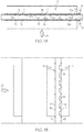
- an exemplary embodiment of an LED panel array 10 is schematically depicted.
- the LED panel array 10 includes a first LED panel 11 and an interfacing second LED panel 14.
- the array 10 may include more than two LED panels.
- the LED panels are disposed parallel to one another.
- the first LED panel 11 may be perpendicularly oriented to an air flow.
- the first LED panel 11 includes a first support or substrate 12, such as a PCB made of any conventional material, such as a metal.
- the first substrate 12 has a first LED side 12a and an opposed first non-LED side 12b.
- the second LED panel 14 includes a second substrate 15, such as a PCB, a second LED side 15a, and a second non-LED side 15b. Thereby, the second non-LED side 15b faces towards each other the first non-LED side 12b.
- one first LED 13 is affixed, advantageously a plurality of first LEDs 13 can be affixed in a first LED array configuration, to the first LED side 12a.
- the first LEDs 13 can be of any conventional design.
- the first LED array configuration can include a random or non-random arrangement of LEDs.
- the first LEDs 13 can be equally spaced from one another in rows and columns.
- LEDs are absent on the first non-LED side 12b.
- the first LED panel 11 includes one first window 21, advantageously a plurality of first windows 21 (i.e., holes or openings) within the first LED array.
- the first LED panel 11 can have first windows 21 that are interspersed, either randomly or non-randomly, among the first LEDs 13.
- the first windows extend from the first LED side 12a, through the first substrate 12, and to the first non-LED side 12b.
- the first windows 21 can be in a first window array configuration whereby each window 21 can be equally spaced from one another in rows and columns.
- LEDs are absent on the first non-LED side 12b.
- the second LED panel 14 includes a support or substrate 15, such as a PCB made of any conventional material, such as a metal.
- a support or substrate 15 such as a PCB made of any conventional material, such as a metal.
- one second LED 17 is affixed, advantageously a plurality of second LEDs 17 can be affixed in a second LED array configuration, to the second LED side 15a.
- the second LEDs 17 can be of any conventional design.
- the second LED array configuration can include a random or non-random arrangement of LEDs.
- the second LEDs 17 can be equally spaced from one another in rows and columns.
- LEDs are absent on the second non-LED side 15b.
- one second window 16 advantageously a plurality of second windows (i.e., openings or holes) 16, extends from the second LED side 15a, through the second substrate 15, and to the second non-LED side 15b.
- the second windows 16 can be arranged in a window array configuration wherein the configuration can include a random or non-random arrangement of windows.
- the second windows 16 can be equally spaced from one another in rows and columns.
- the second windows 16 can be characterized by a window plane 16a that lies in a plane of the second non-LED side 15b.
- the window 16 extends from the non-LED side 15b to the LED side 15a, and each side lies in a respective plane.
- the window 16 also lies in the planes of both sides 15a, 15b. Since a "side" of the window 16 lies in a plane of the non-LED side 15b, the window 16 also has a window plane 16a.
- the first LEDs 13 can be aligned with the second LEDs 17 in both x and y directions.
- the first window 21 is aligned with the second window 16 in both x and y directions.
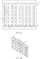
- one air flow diverter 18 is affixed, advantageously a plurality of air flow diverters 18 can be affixed, to and/or integral with the second non-LED side 15b.
- One or more of the diverters 18 includes one or more angled portions 18a that extend from one or more base portions 18b.
- the base portion 18b can be affixed to the second non-LED side 15b.
- a single diverter 18 can include a single base portion 18b with multiple angled portions 18a that extend from opposing edges of the base portion 18b.
- the angled portions 18a are equally spaced from one another along each edge of the base portion 18b.
- One or more of the angled portions 18a can extend from the base portion 18b in such a way that the angled portion 18a extends across or over only a portion of a second window 16, and not all of the second window 16 ( FIG. 2A ). In various embodiments, the angled portion 18a may only extend over about 13% to about 74% of a window 16, thus leaving about 87% to about 26% of the window open (i.e., uncovered or unobstructed).
- one or more of the angled portions 18a can be positioned relative to the window plane 16a at an acute angle 18c.
- the acute angle can be from about 30° to about 75°.
- the angled portion 18a can be positioned relative to the base portion 18b at an obtuse angle from about 105° to about 150°.
- the angled portion 18a may be angled to an impinging air flow 19 described below between about 30° to about 60°.
- one or more the diverters 18 can be made by bending the LED substrate 15.
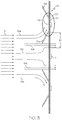
- FIG. 3 schematically depicts a possible mechanism of heat dissipation according to an embodiment of an LED panel belonging to the LED panel array of the present invention.
- the diverter 18 includes angled portions 18a along each opposing edge of the base portion 18b. Air 19 can emanate from the first LED panel 11. As the air 19 meets or contacts a diverter 18, an air portion 19a of the heated air may contact an angled portion 18a, thereby directing the air portion 19a along the second non-LED side 15b, and more specifically, along the base portion 18b.
- Such area of flow along the base portion 18b is depicted by the encircled area 20 and can be referred to as the heat convection area because it is believed that in such area 20 heat transfer by convection occurs.
- an air portion 19b does not contact the angled portion 18a, thereby flowing from the first LED panel 11 and straight or directly into the uncovered portion of the window 16.
- an air portion 19c does not contact the angled portion 18a, thereby flowing from the first LED panel 11 to contact the second non-LED side 15b, and thus indirectly flowing into the uncovered portion of the window 16.
- the change or variation in pressure drop in the system can be minimal.
- FIG. 4 schematically depicts an alternative embodiment of an LED panel array 10'.
- the array 10' is the same as the LED panel array 10, except that the diverter 18' in the former array differs.
- the diverter 18' includes multiple angled portions 18a', but only along one edge of the base portion 18b.
- FIG. 5 schematically depicts a possible mechanism of heat dissipation according to the embodiment of the present invention shown in FIG. 4 .
- Air 19' can emanate from the first LED panel 11. As the air meets or contacts a diverter 18', an air portion 19a' of the air 19' may contact an angled portion 18a', thereby directing the air portion 19a' along the second non-LED side 15b', and more specifically, along the base portion 18b'.
- the area in which the air portion 19a' moves along the base portion 18b' can be referred to as the heat convection area 20'.
- the air portion 19a' may then continue to flow out of the heat convection area 20' and into the uncovered portion of a window 16', which is unlike the embodiment of FIG. 3 .
- an air portion 19b' does not contact the angled portion 18a', thereby flowing from the first LED panel 11 and straight or directly into the uncovered portion of the window 16'.
- an air portion 19c' does not contact the angled portion 18a', but flows along the angled portion 18a' that interfaces the window plane 16a', and into the covered portion of the window 16'.
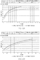
- FIGS. 6A-6C are graphs of temperature versus time of comparative results, under three different operating conditions, for an LED panel without a diverter and the LED panel with the diverter shown in FIG. 1A . It can be seen that over time, the present invention provides a lower operating temperature.
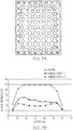
- FIG. 7 is a graph of temperature versus location along an axis of LED panels with diverters according to the embodiments shown in FIGS. 1A and 4 , and an LED panel without diverters.
- the present invention provided a lower operating temperature of about 6°C in the central part of the panel.
- the present invention provided a lower operating temperature of about 8°C in the central part of the panel.
- the present invention can provide a reduction in the second LED panel temperature, over prior art designs, by from about 7% to about 9%.
Landscapes
- Engineering & Computer Science (AREA)
- Microelectronics & Electronic Packaging (AREA)
- General Engineering & Computer Science (AREA)
- Physics & Mathematics (AREA)
- Optics & Photonics (AREA)
- Arrangement Of Elements, Cooling, Sealing, Or The Like Of Lighting Devices (AREA)
Claims (8)
- Leuchtdioden(LED)-Panelanordnung (10 oder 10'), umfassend:ein erstes LED-Panel (11, 11'), einschließend einen ersten Träger (12), der eine erste LED-Seite (12a) und eine erste Nicht-LED-Seite (12b) gegenüber der ersten LED-Seite und ein erstes Fenster (21, 21') aufweist, das sich von der ersten LED-Seite (12a) zur ersten Nicht-LED-Seite (12b) erstreckt;ein zweites LED-Panel (14, 14'), einschließend einen zweiten Träger (15), der eine zweite LED-Seite (15a, 15a'), eine zweite Nicht-LED-Seite (15b, 15b') gegenüber der zweiten LED-Seite und ein zweites Fenster (16, 16') aufweist, das sich von der zweiten LED-Seite (15a, 15a') zur zweiten Nicht-LED-Seite (15b, 15b') erstreckt;eine erste LED (13, 13'), die an der ersten LED-Seite (12a) des ersten LED-Panels (11, 11') befestigt ist;eine zweite LED (17, 17'), die an der zweiten LED-Seite (15a, 15a') des zweiten LED-Panels (14, 14') befestigt ist; und einen Luftstromumlenker (18, 18'), der an der zweiten Nicht-LED-Seite (15b, 15b') des zweiten LED-Panels (14, 14') befestigt ist,wobei das erste LED-Panel (11, 11') parallel zum zweiten LED-Panel (14, 14') angeordnet ist,wobei die erste Nicht-LED-Seite (12b) des ersten LED-Panels (11, 11') zur zweiten Nicht-LED-Seite (15b, 15b') des zweiten LED-Panels (14, 14') weist,wobei der Luftstromumlenker (18, 18') einen gewinkelten Abschnitt (18a, 18a') einschließt,wobei sich der gewinkelte Abschnitt (18a, 18a') über einen Fensterabschnitt erstreckt, der kleiner ist als das gesamte zweite Fenster (16, 16') des zweiten LED-Panels (14, 14'), undwobei das erste Fenster (21, 21') des ersten LED-Panels (11, 11') mit dem zweiten Fenster (16, 16') des zweiten LED-Panels (14, 14') sowohl in x- als auch in y-Richtung ausgerichtet ist.
- LED-Panelanordnung nach Anspruch 1, wobei der erste Träger (12) des ersten LED-Panels (11, 11') und der zweite Träger (15) des zweiten LED-Panels (14, 14') jeweils Leiterplatten (PCB) auf Metallbasis sind.
- LED-Panelanordnung nach einem der Ansprüche 1-2, ferner umfassend eine erste Vielzahl von LEDs (13, 13'), die an der ersten LED-Seite (12a) des ersten LED-Panels (11, 11') befestigt ist, und eine zweite Vielzahl von LEDs (17, 17'), die an der zweiten LED-Seite (15a, 15a') des zweiten LED-Panels (14, 14') befestigt ist.
- LED-Panelanordnung nach einem der Ansprüche 1-3, ferner umfassend eine erste Vielzahl von ersten Fenstern (21, 21'), die sich von der ersten LED-Seite (12a) des ersten LED-Panels (11, 11') zur erste Nicht-LED-Seite (12b) des ersten LED-Panels (11, 11') erstreckt, und eine zweite Vielzahl von zweiten Fenstern (16, 16'), die sich von der zweiten LED-Seite (15a, 15a') des zweiten LED-Panels (14, 14') zur zweiten Nicht-LED-Seite (15b, 15b') des zweiten LED-Panels (14, 14') erstreckt.
- LED-Panelanordnung nach einem der Ansprüche 1-4, ferner umfassend eine Vielzahl von Luftstromumlenkern (18, 18'), die an der zweiten Nicht-LED-Seite (15b, 15b') des zweiten LED-Panels (14, 14') befestigt ist.
- LED-Panelanordnung nach einem der Ansprüche 1-5, wobei das zweite Fenster (16, 16') eine Fensterebene (16a, 16a') einschließt und wobei ein Winkel zwischen der Fensterebene (16a, 16a') und dem gewinkelten Abschnitt (18a, 18a') ein spitzer Winkel ist.
- LED-Panelanordnung nach einem der Ansprüche 1-6, wobei sich der gewinkelte Abschnitt (18a, 18a') nur über ungefähr 13 % bis ungefähr 75 % des zweiten Fensters (16, 16') erstreckt.
- LED-Panelanordnung nach einem der Ansprüche 1-7, wobei der Luftstromumlenker (18, 18') zwei gewinkelte Abschnitte (18a, 18a') einschließt.
Applications Claiming Priority (1)
| Application Number | Priority Date | Filing Date | Title |
|---|---|---|---|
| US14/935,075 US10228117B2 (en) | 2015-11-06 | 2015-11-06 | Air mixing methodology and system to reduce the temperature of LEDs of a photocatalytic reactor |
Publications (2)
| Publication Number | Publication Date |
|---|---|
| EP3166145A1 EP3166145A1 (de) | 2017-05-10 |
| EP3166145B1 true EP3166145B1 (de) | 2020-08-26 |
Family
ID=57609659
Family Applications (1)
| Application Number | Title | Priority Date | Filing Date |
|---|---|---|---|
| EP16195877.2A Active EP3166145B1 (de) | 2015-11-06 | 2016-10-26 | Luftmischsystem zum reduzieren der temperatur von leuchtdioden eines photokatalytischen reaktors |
Country Status (2)
| Country | Link |
|---|---|
| US (1) | US10228117B2 (de) |
| EP (1) | EP3166145B1 (de) |
Family Cites Families (20)
| Publication number | Priority date | Publication date | Assignee | Title |
|---|---|---|---|---|
| US6045240A (en) * | 1996-06-27 | 2000-04-04 | Relume Corporation | LED lamp assembly with means to conduct heat away from the LEDS |
| US6301779B1 (en) | 1998-10-29 | 2001-10-16 | Advanced Thermal Solutions, Inc. | Method for fabricating a heat sink having nested extended surfaces |
| US6753553B2 (en) | 2002-06-17 | 2004-06-22 | Jiahn-Chang Wu | LED matrix substrate with convection holes |
| US7138659B2 (en) | 2004-05-18 | 2006-11-21 | Onscreen Technologies, Inc. | LED assembly with vented circuit board |
| US7096678B2 (en) * | 2004-09-01 | 2006-08-29 | Gelcore Llc | Method and apparatus for increasing natural convection efficiency in long heat sinks |
| TWI449137B (zh) | 2006-03-23 | 2014-08-11 | 製陶技術創新製陶工程股份公司 | 構件或電路用的攜帶體 |
| US7625103B2 (en) * | 2006-04-21 | 2009-12-01 | Cree, Inc. | Multiple thermal path packaging for solid state light emitting apparatus and associated assembling methods |
| US7583502B2 (en) * | 2006-06-13 | 2009-09-01 | Taiwan Semiconductor Manufacturing Co., Ltd. | Method and apparatus for increasing heat dissipation of high performance integrated circuits (IC) |
| US9441824B2 (en) | 2008-04-04 | 2016-09-13 | Cree, Inc. | LED light fixture with heat-dissipation-related high light output |
| US7766514B2 (en) | 2008-06-05 | 2010-08-03 | Hon-Wen Chen | Light emitting diode lamp with high heat-dissipation capacity |
| US8317352B2 (en) * | 2008-12-11 | 2012-11-27 | Robert Saccomanno | Non-invasive injection of light into a transparent substrate, such as a window pane through its face |
| KR101043566B1 (ko) | 2009-03-12 | 2011-06-22 | (주)플레넷아이엔티 | Led 비상등 |
| US9057511B2 (en) * | 2010-03-03 | 2015-06-16 | Cree, Inc. | High efficiency solid state lamp and bulb |
| FR2965042B1 (fr) | 2010-09-22 | 2014-11-21 | Valeo Vision | Dispositif a echange de chaleur, notamment pour vehicule automobile |
| GB201109095D0 (en) | 2011-05-31 | 2011-07-13 | Led Lighting South Africa Close Corp | Cooling of LED illumination devices |
| FR2983030B1 (fr) | 2011-11-17 | 2013-12-27 | Valeo Vision | Dispositif d'evacuation de chaleur pour systeme electronique |
| WO2014037844A1 (en) | 2012-09-05 | 2014-03-13 | Koninklijke Philips N.V | A heat dissipation structure, a lighting device provided with the same and a method of manufacturing the same |
| US10330303B2 (en) * | 2013-11-20 | 2019-06-25 | Lg Electronics Inc. | Light emitting device module with heat-sink and air guide |
| GB2515409B (en) | 2014-07-22 | 2015-05-06 | Wen-Sung Hu | Heat dissipation structure of SMD LED |
| US20160341400A1 (en) * | 2015-05-22 | 2016-11-24 | Posco Led Company Ltd. | Optical semiconductor lighting apparatus |
-
2015
- 2015-11-06 US US14/935,075 patent/US10228117B2/en not_active Expired - Fee Related
-
2016
- 2016-10-26 EP EP16195877.2A patent/EP3166145B1/de active Active
Non-Patent Citations (1)
| Title |
|---|
| None * |
Also Published As
| Publication number | Publication date |
|---|---|
| EP3166145A1 (de) | 2017-05-10 |
| US20170130947A1 (en) | 2017-05-11 |
| US10228117B2 (en) | 2019-03-12 |
Similar Documents
| Publication | Publication Date | Title |
|---|---|---|
| KR101896569B1 (ko) | 반도체 모듈의 방열 장치 | |
| US7534015B2 (en) | LED lamp with a heat dissipation device | |
| US7794116B2 (en) | LED lamp with a heat dissipation device | |
| US7744250B2 (en) | LED lamp with a heat dissipation device | |
| EP1248506B1 (de) | Kuhlkörper für Bauelemente auf einer Leiterplatte | |
| US7695161B2 (en) | Heat dissipation device for light emitting diode module | |
| EP2715226B1 (de) | Kühlung von halbleiterbauelementen | |
| US20170105315A1 (en) | Heat conductive plastic radiator and communicaiton device | |
| US8381799B2 (en) | Heat radiating unit | |
| US20190059177A1 (en) | Heat dissipation module and electronic device | |
| US6930883B2 (en) | Heat-dispersing module of electronic device | |
| KR101992524B1 (ko) | 전자 어셈블리에 걸친 공기 흐름을 재지향시키기 위한 시스템 및 방법 | |
| CN106502340A (zh) | 服务器 | |
| EP3166145B1 (de) | Luftmischsystem zum reduzieren der temperatur von leuchtdioden eines photokatalytischen reaktors | |
| US20100284142A1 (en) | Heat dissipating assembly | |
| KR20160116255A (ko) | 멀티-팬 히트 싱크 | |
| DE102011006779A1 (de) | Anordnung zum Kühlen von elektronischen Bauelementen und/oder Baugruppen | |
| JP2015008225A (ja) | 電子機器 | |
| US20190035709A1 (en) | Electronic modules | |
| US20150068719A1 (en) | Heat sink | |
| KR20230132124A (ko) | 유로 모듈 및 이를 포함하는 전력 기기 | |
| EP3407691B1 (de) | System zur kühlung von rückbeleuchtungseinheiten und elektronischer platten einer anzeigevorrichtung | |
| KR102223236B1 (ko) | 엘이디 조명기구용 히트싱크 | |
| US20120227942A1 (en) | Flow guide structure and thermal module thereof | |
| JP2015216143A (ja) | 発熱素子の放熱構造 |
Legal Events
| Date | Code | Title | Description |
|---|---|---|---|
| PUAI | Public reference made under article 153(3) epc to a published international application that has entered the european phase |
Free format text: ORIGINAL CODE: 0009012 |
|
| STAA | Information on the status of an ep patent application or granted ep patent |
Free format text: STATUS: REQUEST FOR EXAMINATION WAS MADE |
|
| 17P | Request for examination filed |
Effective date: 20161026 |
|
| AK | Designated contracting states |
Kind code of ref document: A1 Designated state(s): AL AT BE BG CH CY CZ DE DK EE ES FI FR GB GR HR HU IE IS IT LI LT LU LV MC MK MT NL NO PL PT RO RS SE SI SK SM TR |
|
| AX | Request for extension of the european patent |
Extension state: BA ME |
|
| GRAP | Despatch of communication of intention to grant a patent |
Free format text: ORIGINAL CODE: EPIDOSNIGR1 |
|
| STAA | Information on the status of an ep patent application or granted ep patent |
Free format text: STATUS: GRANT OF PATENT IS INTENDED |
|
| RIC1 | Information provided on ipc code assigned before grant |
Ipc: F21V 29/74 20150101ALI20200402BHEP Ipc: F21V 29/83 20150101ALI20200402BHEP Ipc: H05K 1/14 20060101ALI20200402BHEP Ipc: H01L 33/64 20100101ALI20200402BHEP Ipc: F21V 29/60 20150101ALN20200402BHEP Ipc: F21Y 105/16 20160101ALN20200402BHEP Ipc: F21Y 115/10 20160101ALN20200402BHEP Ipc: H05K 1/05 20060101ALI20200402BHEP Ipc: H01L 25/075 20060101AFI20200402BHEP |
|
| INTG | Intention to grant announced |
Effective date: 20200420 |
|
| GRAS | Grant fee paid |
Free format text: ORIGINAL CODE: EPIDOSNIGR3 |
|
| GRAA | (expected) grant |
Free format text: ORIGINAL CODE: 0009210 |
|
| STAA | Information on the status of an ep patent application or granted ep patent |
Free format text: STATUS: THE PATENT HAS BEEN GRANTED |
|
| AK | Designated contracting states |
Kind code of ref document: B1 Designated state(s): AL AT BE BG CH CY CZ DE DK EE ES FI FR GB GR HR HU IE IS IT LI LT LU LV MC MK MT NL NO PL PT RO RS SE SI SK SM TR |
|
| REG | Reference to a national code |
Ref country code: GB Ref legal event code: FG4D |
|
| REG | Reference to a national code |
Ref country code: CH Ref legal event code: EP |
|
| REG | Reference to a national code |
Ref country code: AT Ref legal event code: REF Ref document number: 1307209 Country of ref document: AT Kind code of ref document: T Effective date: 20200915 |
|
| REG | Reference to a national code |
Ref country code: IE Ref legal event code: FG4D |
|
| REG | Reference to a national code |
Ref country code: DE Ref legal event code: R096 Ref document number: 602016042658 Country of ref document: DE |
|
| REG | Reference to a national code |
Ref country code: LT Ref legal event code: MG4D |
|
| PG25 | Lapsed in a contracting state [announced via postgrant information from national office to epo] |
Ref country code: PT Free format text: LAPSE BECAUSE OF FAILURE TO SUBMIT A TRANSLATION OF THE DESCRIPTION OR TO PAY THE FEE WITHIN THE PRESCRIBED TIME-LIMIT Effective date: 20201228 Ref country code: FI Free format text: LAPSE BECAUSE OF FAILURE TO SUBMIT A TRANSLATION OF THE DESCRIPTION OR TO PAY THE FEE WITHIN THE PRESCRIBED TIME-LIMIT Effective date: 20200826 Ref country code: SE Free format text: LAPSE BECAUSE OF FAILURE TO SUBMIT A TRANSLATION OF THE DESCRIPTION OR TO PAY THE FEE WITHIN THE PRESCRIBED TIME-LIMIT Effective date: 20200826 Ref country code: HR Free format text: LAPSE BECAUSE OF FAILURE TO SUBMIT A TRANSLATION OF THE DESCRIPTION OR TO PAY THE FEE WITHIN THE PRESCRIBED TIME-LIMIT Effective date: 20200826 Ref country code: GR Free format text: LAPSE BECAUSE OF FAILURE TO SUBMIT A TRANSLATION OF THE DESCRIPTION OR TO PAY THE FEE WITHIN THE PRESCRIBED TIME-LIMIT Effective date: 20201127 Ref country code: NO Free format text: LAPSE BECAUSE OF FAILURE TO SUBMIT A TRANSLATION OF THE DESCRIPTION OR TO PAY THE FEE WITHIN THE PRESCRIBED TIME-LIMIT Effective date: 20201126 Ref country code: LT Free format text: LAPSE BECAUSE OF FAILURE TO SUBMIT A TRANSLATION OF THE DESCRIPTION OR TO PAY THE FEE WITHIN THE PRESCRIBED TIME-LIMIT Effective date: 20200826 Ref country code: BG Free format text: LAPSE BECAUSE OF FAILURE TO SUBMIT A TRANSLATION OF THE DESCRIPTION OR TO PAY THE FEE WITHIN THE PRESCRIBED TIME-LIMIT Effective date: 20201126 |
|
| REG | Reference to a national code |
Ref country code: NL Ref legal event code: MP Effective date: 20200826 |
|
| REG | Reference to a national code |
Ref country code: AT Ref legal event code: MK05 Ref document number: 1307209 Country of ref document: AT Kind code of ref document: T Effective date: 20200826 |
|
| PG25 | Lapsed in a contracting state [announced via postgrant information from national office to epo] |
Ref country code: PL Free format text: LAPSE BECAUSE OF FAILURE TO SUBMIT A TRANSLATION OF THE DESCRIPTION OR TO PAY THE FEE WITHIN THE PRESCRIBED TIME-LIMIT Effective date: 20200826 Ref country code: NL Free format text: LAPSE BECAUSE OF FAILURE TO SUBMIT A TRANSLATION OF THE DESCRIPTION OR TO PAY THE FEE WITHIN THE PRESCRIBED TIME-LIMIT Effective date: 20200826 Ref country code: LV Free format text: LAPSE BECAUSE OF FAILURE TO SUBMIT A TRANSLATION OF THE DESCRIPTION OR TO PAY THE FEE WITHIN THE PRESCRIBED TIME-LIMIT Effective date: 20200826 Ref country code: RS Free format text: LAPSE BECAUSE OF FAILURE TO SUBMIT A TRANSLATION OF THE DESCRIPTION OR TO PAY THE FEE WITHIN THE PRESCRIBED TIME-LIMIT Effective date: 20200826 Ref country code: IS Free format text: LAPSE BECAUSE OF FAILURE TO SUBMIT A TRANSLATION OF THE DESCRIPTION OR TO PAY THE FEE WITHIN THE PRESCRIBED TIME-LIMIT Effective date: 20201226 |
|
| PG25 | Lapsed in a contracting state [announced via postgrant information from national office to epo] |
Ref country code: EE Free format text: LAPSE BECAUSE OF FAILURE TO SUBMIT A TRANSLATION OF THE DESCRIPTION OR TO PAY THE FEE WITHIN THE PRESCRIBED TIME-LIMIT Effective date: 20200826 Ref country code: RO Free format text: LAPSE BECAUSE OF FAILURE TO SUBMIT A TRANSLATION OF THE DESCRIPTION OR TO PAY THE FEE WITHIN THE PRESCRIBED TIME-LIMIT Effective date: 20200826 Ref country code: SM Free format text: LAPSE BECAUSE OF FAILURE TO SUBMIT A TRANSLATION OF THE DESCRIPTION OR TO PAY THE FEE WITHIN THE PRESCRIBED TIME-LIMIT Effective date: 20200826 Ref country code: CZ Free format text: LAPSE BECAUSE OF FAILURE TO SUBMIT A TRANSLATION OF THE DESCRIPTION OR TO PAY THE FEE WITHIN THE PRESCRIBED TIME-LIMIT Effective date: 20200826 Ref country code: DK Free format text: LAPSE BECAUSE OF FAILURE TO SUBMIT A TRANSLATION OF THE DESCRIPTION OR TO PAY THE FEE WITHIN THE PRESCRIBED TIME-LIMIT Effective date: 20200826 |
|
| REG | Reference to a national code |
Ref country code: DE Ref legal event code: R097 Ref document number: 602016042658 Country of ref document: DE |
|
| PG25 | Lapsed in a contracting state [announced via postgrant information from national office to epo] |
Ref country code: ES Free format text: LAPSE BECAUSE OF FAILURE TO SUBMIT A TRANSLATION OF THE DESCRIPTION OR TO PAY THE FEE WITHIN THE PRESCRIBED TIME-LIMIT Effective date: 20200826 Ref country code: AL Free format text: LAPSE BECAUSE OF FAILURE TO SUBMIT A TRANSLATION OF THE DESCRIPTION OR TO PAY THE FEE WITHIN THE PRESCRIBED TIME-LIMIT Effective date: 20200826 Ref country code: AT Free format text: LAPSE BECAUSE OF FAILURE TO SUBMIT A TRANSLATION OF THE DESCRIPTION OR TO PAY THE FEE WITHIN THE PRESCRIBED TIME-LIMIT Effective date: 20200826 |
|
| REG | Reference to a national code |
Ref country code: CH Ref legal event code: PL |
|
| PG25 | Lapsed in a contracting state [announced via postgrant information from national office to epo] |
Ref country code: MC Free format text: LAPSE BECAUSE OF FAILURE TO SUBMIT A TRANSLATION OF THE DESCRIPTION OR TO PAY THE FEE WITHIN THE PRESCRIBED TIME-LIMIT Effective date: 20200826 Ref country code: LU Free format text: LAPSE BECAUSE OF NON-PAYMENT OF DUE FEES Effective date: 20201026 Ref country code: SK Free format text: LAPSE BECAUSE OF FAILURE TO SUBMIT A TRANSLATION OF THE DESCRIPTION OR TO PAY THE FEE WITHIN THE PRESCRIBED TIME-LIMIT Effective date: 20200826 |
|
| PLBE | No opposition filed within time limit |
Free format text: ORIGINAL CODE: 0009261 |
|
| STAA | Information on the status of an ep patent application or granted ep patent |
Free format text: STATUS: NO OPPOSITION FILED WITHIN TIME LIMIT |
|
| REG | Reference to a national code |
Ref country code: BE Ref legal event code: MM Effective date: 20201031 |
|
| PG25 | Lapsed in a contracting state [announced via postgrant information from national office to epo] |
Ref country code: IT Free format text: LAPSE BECAUSE OF FAILURE TO SUBMIT A TRANSLATION OF THE DESCRIPTION OR TO PAY THE FEE WITHIN THE PRESCRIBED TIME-LIMIT Effective date: 20200826 Ref country code: FR Free format text: LAPSE BECAUSE OF NON-PAYMENT OF DUE FEES Effective date: 20201026 |
|
| 26N | No opposition filed |
Effective date: 20210527 |
|
| PG25 | Lapsed in a contracting state [announced via postgrant information from national office to epo] |
Ref country code: CH Free format text: LAPSE BECAUSE OF NON-PAYMENT OF DUE FEES Effective date: 20201031 Ref country code: BE Free format text: LAPSE BECAUSE OF NON-PAYMENT OF DUE FEES Effective date: 20201031 Ref country code: SI Free format text: LAPSE BECAUSE OF FAILURE TO SUBMIT A TRANSLATION OF THE DESCRIPTION OR TO PAY THE FEE WITHIN THE PRESCRIBED TIME-LIMIT Effective date: 20200826 Ref country code: LI Free format text: LAPSE BECAUSE OF NON-PAYMENT OF DUE FEES Effective date: 20201031 |
|
| PG25 | Lapsed in a contracting state [announced via postgrant information from national office to epo] |
Ref country code: IE Free format text: LAPSE BECAUSE OF NON-PAYMENT OF DUE FEES Effective date: 20201026 |
|
| PGFP | Annual fee paid to national office [announced via postgrant information from national office to epo] |
Ref country code: GB Payment date: 20211026 Year of fee payment: 6 Ref country code: DE Payment date: 20211027 Year of fee payment: 6 |
|
| PG25 | Lapsed in a contracting state [announced via postgrant information from national office to epo] |
Ref country code: TR Free format text: LAPSE BECAUSE OF FAILURE TO SUBMIT A TRANSLATION OF THE DESCRIPTION OR TO PAY THE FEE WITHIN THE PRESCRIBED TIME-LIMIT Effective date: 20200826 Ref country code: MT Free format text: LAPSE BECAUSE OF FAILURE TO SUBMIT A TRANSLATION OF THE DESCRIPTION OR TO PAY THE FEE WITHIN THE PRESCRIBED TIME-LIMIT Effective date: 20200826 Ref country code: CY Free format text: LAPSE BECAUSE OF FAILURE TO SUBMIT A TRANSLATION OF THE DESCRIPTION OR TO PAY THE FEE WITHIN THE PRESCRIBED TIME-LIMIT Effective date: 20200826 |
|
| PG25 | Lapsed in a contracting state [announced via postgrant information from national office to epo] |
Ref country code: MK Free format text: LAPSE BECAUSE OF FAILURE TO SUBMIT A TRANSLATION OF THE DESCRIPTION OR TO PAY THE FEE WITHIN THE PRESCRIBED TIME-LIMIT Effective date: 20200826 |
|
| REG | Reference to a national code |
Ref country code: DE Ref legal event code: R119 Ref document number: 602016042658 Country of ref document: DE |
|
| GBPC | Gb: european patent ceased through non-payment of renewal fee |
Effective date: 20221026 |
|
| P01 | Opt-out of the competence of the unified patent court (upc) registered |
Effective date: 20230525 |
|
| PG25 | Lapsed in a contracting state [announced via postgrant information from national office to epo] |
Ref country code: DE Free format text: LAPSE BECAUSE OF NON-PAYMENT OF DUE FEES Effective date: 20230503 |
|
| PG25 | Lapsed in a contracting state [announced via postgrant information from national office to epo] |
Ref country code: GB Free format text: LAPSE BECAUSE OF NON-PAYMENT OF DUE FEES Effective date: 20221026 |