EP3157317A1 - Shielding case, pcb and terminal device - Google Patents
Shielding case, pcb and terminal device Download PDFInfo
- Publication number
- EP3157317A1 EP3157317A1 EP16158530.2A EP16158530A EP3157317A1 EP 3157317 A1 EP3157317 A1 EP 3157317A1 EP 16158530 A EP16158530 A EP 16158530A EP 3157317 A1 EP3157317 A1 EP 3157317A1
- Authority
- EP
- European Patent Office
- Prior art keywords
- shielding case
- case body
- top wall
- side wall
- storage material
- Prior art date
- Legal status (The legal status is an assumption and is not a legal conclusion. Google has not performed a legal analysis and makes no representation as to the accuracy of the status listed.)
- Granted
Links
Images


Classifications
-
- H—ELECTRICITY
- H05—ELECTRIC TECHNIQUES NOT OTHERWISE PROVIDED FOR
- H05K—PRINTED CIRCUITS; CASINGS OR CONSTRUCTIONAL DETAILS OF ELECTRIC APPARATUS; MANUFACTURE OF ASSEMBLAGES OF ELECTRICAL COMPONENTS
- H05K7/00—Constructional details common to different types of electric apparatus
- H05K7/20—Modifications to facilitate cooling, ventilating, or heating
-
- H—ELECTRICITY
- H04—ELECTRIC COMMUNICATION TECHNIQUE
- H04M—TELEPHONIC COMMUNICATION
- H04M1/00—Substation equipment, e.g. for use by subscribers
- H04M1/02—Constructional features of telephone sets
- H04M1/0202—Portable telephone sets, e.g. cordless phones, mobile phones or bar type handsets
-
- H—ELECTRICITY
- H05—ELECTRIC TECHNIQUES NOT OTHERWISE PROVIDED FOR
- H05K—PRINTED CIRCUITS; CASINGS OR CONSTRUCTIONAL DETAILS OF ELECTRIC APPARATUS; MANUFACTURE OF ASSEMBLAGES OF ELECTRICAL COMPONENTS
- H05K1/00—Printed circuits
- H05K1/02—Details
- H05K1/0201—Thermal arrangements, e.g. for cooling, heating or preventing overheating
- H05K1/0212—Printed circuits or mounted components having integral heating means
-
- H—ELECTRICITY
- H05—ELECTRIC TECHNIQUES NOT OTHERWISE PROVIDED FOR
- H05K—PRINTED CIRCUITS; CASINGS OR CONSTRUCTIONAL DETAILS OF ELECTRIC APPARATUS; MANUFACTURE OF ASSEMBLAGES OF ELECTRICAL COMPONENTS
- H05K5/00—Casings, cabinets or drawers for electric apparatus
- H05K5/0026—Casings, cabinets or drawers for electric apparatus provided with connectors and printed circuit boards [PCB], e.g. automotive electronic control units
-
- H—ELECTRICITY
- H05—ELECTRIC TECHNIQUES NOT OTHERWISE PROVIDED FOR
- H05K—PRINTED CIRCUITS; CASINGS OR CONSTRUCTIONAL DETAILS OF ELECTRIC APPARATUS; MANUFACTURE OF ASSEMBLAGES OF ELECTRICAL COMPONENTS
- H05K5/00—Casings, cabinets or drawers for electric apparatus
- H05K5/0026—Casings, cabinets or drawers for electric apparatus provided with connectors and printed circuit boards [PCB], e.g. automotive electronic control units
- H05K5/0047—Casings, cabinets or drawers for electric apparatus provided with connectors and printed circuit boards [PCB], e.g. automotive electronic control units having a two-part housing enclosing a PCB
-
- H—ELECTRICITY
- H05—ELECTRIC TECHNIQUES NOT OTHERWISE PROVIDED FOR
- H05K—PRINTED CIRCUITS; CASINGS OR CONSTRUCTIONAL DETAILS OF ELECTRIC APPARATUS; MANUFACTURE OF ASSEMBLAGES OF ELECTRICAL COMPONENTS
- H05K5/00—Casings, cabinets or drawers for electric apparatus
- H05K5/02—Details
- H05K5/0209—Thermal insulation, e.g. for fire protection or for fire containment or for high temperature environments
- H05K5/0211—Thermal buffers, e.g. latent heat absorbers
-
- H—ELECTRICITY
- H05—ELECTRIC TECHNIQUES NOT OTHERWISE PROVIDED FOR
- H05K—PRINTED CIRCUITS; CASINGS OR CONSTRUCTIONAL DETAILS OF ELECTRIC APPARATUS; MANUFACTURE OF ASSEMBLAGES OF ELECTRICAL COMPONENTS
- H05K7/00—Constructional details common to different types of electric apparatus
- H05K7/20—Modifications to facilitate cooling, ventilating, or heating
- H05K7/2039—Modifications to facilitate cooling, ventilating, or heating characterised by the heat transfer by conduction from the heat generating element to a dissipating body
- H05K7/20518—Unevenly distributed heat load, e.g. different sectors at different temperatures, localised cooling, hot spots
-
- H—ELECTRICITY
- H05—ELECTRIC TECHNIQUES NOT OTHERWISE PROVIDED FOR
- H05K—PRINTED CIRCUITS; CASINGS OR CONSTRUCTIONAL DETAILS OF ELECTRIC APPARATUS; MANUFACTURE OF ASSEMBLAGES OF ELECTRICAL COMPONENTS
- H05K9/00—Screening of apparatus or components against electric or magnetic fields
- H05K9/0007—Casings
- H05K9/002—Casings with localised screening
- H05K9/0022—Casings with localised screening of components mounted on printed circuit boards [PCB]
- H05K9/0024—Shield cases mounted on a PCB, e.g. cans or caps or conformal shields
-
- H—ELECTRICITY
- H05—ELECTRIC TECHNIQUES NOT OTHERWISE PROVIDED FOR
- H05K—PRINTED CIRCUITS; CASINGS OR CONSTRUCTIONAL DETAILS OF ELECTRIC APPARATUS; MANUFACTURE OF ASSEMBLAGES OF ELECTRICAL COMPONENTS
- H05K9/00—Screening of apparatus or components against electric or magnetic fields
- H05K9/0007—Casings
- H05K9/002—Casings with localised screening
- H05K9/0022—Casings with localised screening of components mounted on printed circuit boards [PCB]
- H05K9/0024—Shield cases mounted on a PCB, e.g. cans or caps or conformal shields
- H05K9/0026—Shield cases mounted on a PCB, e.g. cans or caps or conformal shields integrally formed from metal sheet
-
- H—ELECTRICITY
- H05—ELECTRIC TECHNIQUES NOT OTHERWISE PROVIDED FOR
- H05K—PRINTED CIRCUITS; CASINGS OR CONSTRUCTIONAL DETAILS OF ELECTRIC APPARATUS; MANUFACTURE OF ASSEMBLAGES OF ELECTRICAL COMPONENTS
- H05K9/00—Screening of apparatus or components against electric or magnetic fields
- H05K9/0007—Casings
- H05K9/002—Casings with localised screening
- H05K9/0022—Casings with localised screening of components mounted on printed circuit boards [PCB]
- H05K9/0024—Shield cases mounted on a PCB, e.g. cans or caps or conformal shields
- H05K9/0032—Shield cases mounted on a PCB, e.g. cans or caps or conformal shields having multiple parts, e.g. frames mating with lids
-
- H—ELECTRICITY
- H10—SEMICONDUCTOR DEVICES; ELECTRIC SOLID-STATE DEVICES NOT OTHERWISE PROVIDED FOR
- H10W—GENERIC PACKAGES, INTERCONNECTIONS, CONNECTORS OR OTHER CONSTRUCTIONAL DETAILS OF DEVICES COVERED BY CLASS H10
- H10W40/00—Arrangements for thermal protection or thermal control
-
- H—ELECTRICITY
- H10—SEMICONDUCTOR DEVICES; ELECTRIC SOLID-STATE DEVICES NOT OTHERWISE PROVIDED FOR
- H10W—GENERIC PACKAGES, INTERCONNECTIONS, CONNECTORS OR OTHER CONSTRUCTIONAL DETAILS OF DEVICES COVERED BY CLASS H10
- H10W40/00—Arrangements for thermal protection or thermal control
- H10W40/70—Fillings or auxiliary members in containers or in encapsulations for thermal protection or control
-
- H—ELECTRICITY
- H05—ELECTRIC TECHNIQUES NOT OTHERWISE PROVIDED FOR
- H05K—PRINTED CIRCUITS; CASINGS OR CONSTRUCTIONAL DETAILS OF ELECTRIC APPARATUS; MANUFACTURE OF ASSEMBLAGES OF ELECTRICAL COMPONENTS
- H05K2201/00—Indexing scheme relating to printed circuits covered by H05K1/00
- H05K2201/06—Thermal details
- H05K2201/066—Heatsink mounted on the surface of the printed circuit board [PCB]
-
- H—ELECTRICITY
- H05—ELECTRIC TECHNIQUES NOT OTHERWISE PROVIDED FOR
- H05K—PRINTED CIRCUITS; CASINGS OR CONSTRUCTIONAL DETAILS OF ELECTRIC APPARATUS; MANUFACTURE OF ASSEMBLAGES OF ELECTRICAL COMPONENTS
- H05K2201/00—Indexing scheme relating to printed circuits covered by H05K1/00
- H05K2201/07—Electric details
- H05K2201/0707—Shielding
-
- H—ELECTRICITY
- H05—ELECTRIC TECHNIQUES NOT OTHERWISE PROVIDED FOR
- H05K—PRINTED CIRCUITS; CASINGS OR CONSTRUCTIONAL DETAILS OF ELECTRIC APPARATUS; MANUFACTURE OF ASSEMBLAGES OF ELECTRICAL COMPONENTS
- H05K2201/00—Indexing scheme relating to printed circuits covered by H05K1/00
- H05K2201/10—Details of components or other objects attached to or integrated in a printed circuit board
- H05K2201/10227—Other objects, e.g. metallic pieces
- H05K2201/10371—Shields or metal cases
-
- H—ELECTRICITY
- H05—ELECTRIC TECHNIQUES NOT OTHERWISE PROVIDED FOR
- H05K—PRINTED CIRCUITS; CASINGS OR CONSTRUCTIONAL DETAILS OF ELECTRIC APPARATUS; MANUFACTURE OF ASSEMBLAGES OF ELECTRICAL COMPONENTS
- H05K7/00—Constructional details common to different types of electric apparatus
- H05K7/20—Modifications to facilitate cooling, ventilating, or heating
- H05K7/2039—Modifications to facilitate cooling, ventilating, or heating characterised by the heat transfer by conduction from the heat generating element to a dissipating body
-
- H—ELECTRICITY
- H05—ELECTRIC TECHNIQUES NOT OTHERWISE PROVIDED FOR
- H05K—PRINTED CIRCUITS; CASINGS OR CONSTRUCTIONAL DETAILS OF ELECTRIC APPARATUS; MANUFACTURE OF ASSEMBLAGES OF ELECTRICAL COMPONENTS
- H05K7/00—Constructional details common to different types of electric apparatus
- H05K7/20—Modifications to facilitate cooling, ventilating, or heating
- H05K7/2039—Modifications to facilitate cooling, ventilating, or heating characterised by the heat transfer by conduction from the heat generating element to a dissipating body
- H05K7/20409—Outer radiating structures on heat dissipating housings, e.g. fins integrated with the housing
- H05K7/20418—Outer radiating structures on heat dissipating housings, e.g. fins integrated with the housing the radiating structures being additional and fastened onto the housing
-
- H—ELECTRICITY
- H05—ELECTRIC TECHNIQUES NOT OTHERWISE PROVIDED FOR
- H05K—PRINTED CIRCUITS; CASINGS OR CONSTRUCTIONAL DETAILS OF ELECTRIC APPARATUS; MANUFACTURE OF ASSEMBLAGES OF ELECTRICAL COMPONENTS
- H05K7/00—Constructional details common to different types of electric apparatus
- H05K7/20—Modifications to facilitate cooling, ventilating, or heating
- H05K7/2039—Modifications to facilitate cooling, ventilating, or heating characterised by the heat transfer by conduction from the heat generating element to a dissipating body
- H05K7/20409—Outer radiating structures on heat dissipating housings, e.g. fins integrated with the housing
- H05K7/20427—Outer radiating structures on heat dissipating housings, e.g. fins integrated with the housing having radiation enhancing surface treatment, e.g. black coating
-
- H—ELECTRICITY
- H05—ELECTRIC TECHNIQUES NOT OTHERWISE PROVIDED FOR
- H05K—PRINTED CIRCUITS; CASINGS OR CONSTRUCTIONAL DETAILS OF ELECTRIC APPARATUS; MANUFACTURE OF ASSEMBLAGES OF ELECTRICAL COMPONENTS
- H05K7/00—Constructional details common to different types of electric apparatus
- H05K7/20—Modifications to facilitate cooling, ventilating, or heating
- H05K7/2039—Modifications to facilitate cooling, ventilating, or heating characterised by the heat transfer by conduction from the heat generating element to a dissipating body
- H05K7/20436—Inner thermal coupling elements in heat dissipating housings, e.g. protrusions or depressions integrally formed in the housing
-
- H—ELECTRICITY
- H05—ELECTRIC TECHNIQUES NOT OTHERWISE PROVIDED FOR
- H05K—PRINTED CIRCUITS; CASINGS OR CONSTRUCTIONAL DETAILS OF ELECTRIC APPARATUS; MANUFACTURE OF ASSEMBLAGES OF ELECTRICAL COMPONENTS
- H05K9/00—Screening of apparatus or components against electric or magnetic fields
- H05K9/0007—Casings
- H05K9/0052—Shielding other than Faraday cages
-
- H—ELECTRICITY
- H05—ELECTRIC TECHNIQUES NOT OTHERWISE PROVIDED FOR
- H05K—PRINTED CIRCUITS; CASINGS OR CONSTRUCTIONAL DETAILS OF ELECTRIC APPARATUS; MANUFACTURE OF ASSEMBLAGES OF ELECTRICAL COMPONENTS
- H05K9/00—Screening of apparatus or components against electric or magnetic fields
- H05K9/0073—Shielding materials
- H05K9/0081—Electromagnetic shielding materials, e.g. EMI, RFI shielding
Definitions
- the present disclosure generally relates to the shield of electronic components, and more particularly, to a shielding case, a Printed Circuit Board (PCB) using the shielding case and a terminal device using the PCB.
- PCB Printed Circuit Board
- the present invention provides a shielding case, a PCB and a terminal device.
- the invention relates to a shielding case, which includes: a first shielding case body and a second shielding case body that are interconnected, wherein the first shielding case body has a first top wall and a first side wall, the second shielding case body has a second top wall and a second side wall, wherein the second shielding case body at least partially covers the first shielding case body, and a heat storage material is accommodated between the first shielding case body and the second shielding case body.
- the second shielding case body may at least partially, particularly wholly, cover the first top wall.
- a cross section area of the second shielding case body may be less than that of the first shielding case body, and a bottom of the second side wall may be welded on the first top wall.
- the second shielding case body may cover both the first top wall and the first side wall.
- the second shielding case body may be connected with the first shielding case body through multiple joint pins that are arranged along a circumference direction at intervals; an inner end of the joint pin may be connected with a corner between the first top wall and the first side wall, while an outer end may be connected with a corner between the second top wall and the second side wall;
- the heat storage material may include a first heat storage material located between the first top wall and the second top wall and a second heat storage material located between the first side wall and the second side wall.
- multiple ventilation holes distributed at intervals may be formed on the second shielding case body.
- the invention relates to a PCB, which includes: a board body and a heating component disposed on the board body, wherein a shielding case that is described in the above embodiment of the present disclosure covers the heating component, and the shielding case is connected onto the board body; or, a first shielding case body covers the heating component, a second shielding case body at least partially covers the first shielding case body, the first shielding case body and the second shielding case body are connected onto the board body respectively, and a heat storage material is accommodated between the first shielding case body and the second shielding case body.
- the invention relates to a terminal device, which includes a PCB described in the above embodiment of the present disclosure provided in the terminal device.
- the terminal device may be a mobile phone or a tablet computer.
- the heat storage material accommodated between the two shielding case bodies can absorb and store the heat radiated by a heating component and then gradually dissipates the heat; therefore, the present disclosure not only realizes the dissipation of heat from a heating component that is running at a high speed, but also avoids the dissipated heat being directly radiated onto the outside of a terminal device to impact user experience; moreover, the double-layer structure has a big superficial surface for absorbing heat, which strengthens the effect of heat control.
- Position words employed hereinafter such as “upper, lower, left, right” generally are relative to the surface direction of a corresponding accompanying drawing if no particular description is specified, and specifically can refer to the surface direction as shown in Fig. 1 to Fig. 3 ; “inner and outer” refer to the inner side and outer side of the profile of a corresponding part.
- exemplary embodiments of the present disclosure provide a shielding case, a PCB and a terminal device, wherein the terminal device may be a device a user often needs to handheld, such as a mobile phone, a tablet computer and the like.
- the significant heating source of the terminal device is a heating component 5 on the PCB, for example, a master chip. This type of heating component 5 will release a large amount of heat while running at a high speed.
- An exemplary embodiment of the present disclosure can effectively control the impact of the heat radiation of the heating component 5 onto user experience.
- first and second exemplary embodiments of the present disclosure provide a PCB, including: a board body 4 and a heating component 5 disposed on the board body 4, wherein a shielding case is covered on the heating component 5, and the shielding case is connected onto the board body 4, for example, welded onto the board body 4.
- the shielding case itself can shield the radiation from an element that is running at a high speed (such as the heating component 5), to prevent the interference onto other elements; the shielding case can be made of stainless steel or copper-nickel alloy and other shielding materials.
- the shielding case provided in exemplary embodiments of the present disclosure includes: a first shielding case body 1 and a second shielding case body 2 that are interconnected, wherein the first shielding case body 1 has a first top wall 11 and a first side wall 12, the second shielding case body 2 has a second top wall 21 and a second side wall 22, the side walls of the two shielding case bodies can extend downwards from the top wall perpendicularly or extend slantwise slightly, to form a shield shaped structure.
- the second shielding case body 2 at least partially covers the first shielding case body 1, and a heat storage material 3 is accommodated between the first shielding case body 1 and the second shielding case body 2.
- the heat storage material 3 accommodated between the two shielding case bodies can absorb and store the heat radiated by a heating component 5 and then gradually dissipates the heat; therefore, the present disclosure not only realizes the dissipation of heat from the heating component 5 that is running at a high speed, but also avoids the dissipated heat being directly radiated onto the outside of a terminal device to impact user experience; moreover, the double-layer structure has a big superficial surface for absorbing heat, which strengthens the effect of heat control.
- the shielding case body can be designed to be more layers, which depend on the volume of the terminal device and the heating control effect.
- the heat storage material 3 can adopt a material with a lower heat conductivity coefficient, for example, silica gel with a lower heat conductivity coefficient.
- the second shielding case body 2 at least partially covers the first top wall 11; thus, the top wall 11 in the first shielding case body 1 having a relatively big area bears the heat storage material 3; further, it is simple to mount the first shielding case body onto the board body 4 of the PCB, specifically, it is only needed to weld the bottom of the first side wall 12 onto the board body 4.
- the two shielding case bodies can be stamped respectively and then are welded mutually; to better connect the two shielding case bodies, the cross section area of the second shielding case body 2 is less than that of the first shielding case body 1; the bottom of the second side wall 22 of the smaller second shielding case body 2 can be conveniently welded onto the first top wall 11 of the first shielding case body 1.
- the cross section areas of the two shielding case bodies might be the same; the two shielding case bodies, or, the two shielding case bodies and the board body 4 can be connected by a demountable method such as clamping and plug-in.
- the second shielding case body 2 covers both the first top wall 11 and the first side wall 12. In this way, when the heating component 5 is operating, the heat radiated from the heating component 5 can be absorbed and stored by both the top and side walls, thus the heat of the terminal device can be controlled.
- the second shielding case body 2 is connected with the first shielding case body 1 through multiple joint pins 23 that are arranged along the circumference direction at intervals; an inner end of the joint pin 23 is connected with a corner between the first top wall and the first side wall, while an outer end is connected with a corner between the second top wall and the second side wall; in this way, the heat storage material 3 may include a first heat storage material 31 located between the first top wall and the second top wall, for example, a plate shaped heat storage material, and a second heat storage material 32 located between the first side wall and the second side wall, for example, a ring shaped heat storage material. Since there are gaps among the multiple joint pins 23, the space between the two shielding case bodies is interconnected, so that the two heat storage materials 3 can mutually cooperate to better absorb and store heat from the top and side walls of the heating component 5.
- the first heat storage material 31 and the second heat storage material 32 can be integrated, that is so say, through holes for the joint pins 23 to pass through are formed on the integrated structure, or, the first heat storage material and the second heat storage material are independent, that is to say, they are assembled between the top walls, between the side walls of the two shielding case bodies respectively.
- the two shielding case bodies can also be connected through joint pins located at the corners, wherein the joint pin can also be disposed on the top wall or the side wall.
- both the shielding case bodies are of a whole structure; however, as shown in Fig. 3 , in a third exemplary embodiment of the present disclosure, the two shielding case bodies may be not directly connected; in this way, the first shielding case body 1 covers the heating component 5, the second shielding case body 2 covers the first shielding case body 1, the first shielding case body 1 and the second shielding case body 2 are interconnected by being connected onto the board body 4 respectively, for example, by welding, moreover a heat storage material 3 is accommodated between the first shielding case body 1 and the second shielding case body 2.
- the third embodiment can also accomplish the heat control on the heating component 5 through the heat storage material disposed between the two shielding case bodies.
- the two shielding case bodies can be the same as or similar to the two shielding case bodies in the second embodiment in structure; the heat storage material 3 between the two shielding case bodies can be disposed between the top walls and between the side walls at the same time, or, between top walls only in other possible embodiments.
- multiple ventilation holes 24 distributed at intervals are formed on the second shielding case body 2.
- the heat storage material can dissipate heat after absorbing and storing the heat, thereby reducing the heat absorption load of the heat storage material.
- similar ventilation holes 24 can be formed on the second shielding case body 2 in other embodiments.
- the shape of the shielding case body can be determined according to the number and layout of the electronic elements to be covered.
- a heat storage material accommodated between two shielding case bodies can absorb and store heat radiated by a heating component and then gradually dissipates the heat; therefore, the present disclosure not only realizes the dissipation of heat from the heating component that is running at a high speed, but also avoids the dissipated heat being directly radiated onto the outside of a terminal device to impact user experience; moreover, the double-layer structure has a big superficial surface for absorbing the heat, which strengthens the effect of heat control.
Landscapes
- Engineering & Computer Science (AREA)
- Microelectronics & Electronic Packaging (AREA)
- Physics & Mathematics (AREA)
- Thermal Sciences (AREA)
- Signal Processing (AREA)
- Cooling Or The Like Of Electrical Apparatus (AREA)
- Shielding Devices Or Components To Electric Or Magnetic Fields (AREA)
- Telephone Set Structure (AREA)
- Casings For Electric Apparatus (AREA)
- Distribution Board (AREA)
- Details Of Aerials (AREA)
- Cooling Or The Like Of Semiconductors Or Solid State Devices (AREA)
Abstract
Description
- The present disclosure generally relates to the shield of electronic components, and more particularly, to a shielding case, a Printed Circuit Board (PCB) using the shielding case and a terminal device using the PCB.
- With the development of economy and society, people have a growing demand on the performance of terminal devices such as a mobile phone. Accordingly, the power consumption of the electronic components is increasing; therefore, heat dissipation becomes a problem all manufacturers must confront with.
- Accordingly, the present invention provides a shielding case, a PCB and a terminal device.
- According to a first aspect, the invention relates to a shielding case, which includes: a first shielding case body and a second shielding case body that are interconnected, wherein the first shielding case body has a first top wall and a first side wall, the second shielding case body has a second top wall and a second side wall, wherein the second shielding case body at least partially covers the first shielding case body, and a heat storage material is accommodated between the first shielding case body and the second shielding case body.
- According to an exemplary embodiment, the second shielding case body may at least partially, particularly wholly, cover the first top wall.
- According to an exemplary embodiment, a cross section area of the second shielding case body may be less than that of the first shielding case body, and a bottom of the second side wall may be welded on the first top wall.
- According to an exemplary embodiment, the second shielding case body may cover both the first top wall and the first side wall.
- According to an exemplary embodiment, the second shielding case body may be connected with the first shielding case body through multiple joint pins that are arranged along a circumference direction at intervals; an inner end of the joint pin may be connected with a corner between the first top wall and the first side wall, while an outer end may be connected with a corner between the second top wall and the second side wall; the heat storage material may include a first heat storage material located between the first top wall and the second top wall and a second heat storage material located between the first side wall and the second side wall.
- According to an exemplary embodiment, multiple ventilation holes distributed at intervals may be formed on the second shielding case body.
- According to a second aspect, the invention relates to a PCB, which includes: a board body and a heating component disposed on the board body, wherein a shielding case that is described in the above embodiment of the present disclosure covers the heating component, and the shielding case is connected onto the board body; or, a first shielding case body covers the heating component, a second shielding case body at least partially covers the first shielding case body, the first shielding case body and the second shielding case body are connected onto the board body respectively, and a heat storage material is accommodated between the first shielding case body and the second shielding case body.
- According to a third aspect, the invention relates to a terminal device, which includes a PCB described in the above embodiment of the present disclosure provided in the terminal device.
- According to an exemplary embodiment, the terminal device may be a mobile phone or a tablet computer.
- The technical scheme provided in the embodiment of the present disclosure has following advantages: the heat storage material accommodated between the two shielding case bodies can absorb and store the heat radiated by a heating component and then gradually dissipates the heat; therefore, the present disclosure not only realizes the dissipation of heat from a heating component that is running at a high speed, but also avoids the dissipated heat being directly radiated onto the outside of a terminal device to impact user experience; moreover, the double-layer structure has a big superficial surface for absorbing heat, which strengthens the effect of heat control.
- It is to be understood that both the foregoing general description and the following detailed description are exemplary and explanatory only and are not restrictive of the invention, as claimed.
- The accompanying drawings, which are incorporated in and constitute a part of this specification, illustrate embodiments consistent with the invention and, together with the description, serve to explain the principles of the invention.
-
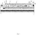
Fig. 1 is a section diagram of a PCB, according to a first exemplary embodiment. -
Fig. 2 is a section diagram of a PCB, according to a second exemplary embodiment. -
Fig. 3 is a section diagram of a PCB, according to a third exemplary embodiment. -
Fig. 4 is a structure stereogram of a shielding case, according to the first exemplary embodiment. - Reference will now be made in detail to exemplary embodiments, examples of which are illustrated in the accompanying drawings. The following description refers to the accompanying drawings in which the same numbers in different drawings represent the same or similar elements unless otherwise represented. The implementations set forth in the following description of exemplary embodiments do not represent all implementations consistent with the invention. Instead, they are merely examples of apparatuses and methods consistent with aspects related to the invention as recited in the appended claims.
- Position words employed hereinafter such as "upper, lower, left, right" generally are relative to the surface direction of a corresponding accompanying drawing if no particular description is specified, and specifically can refer to the surface direction as shown in
Fig. 1 to Fig. 3 ; "inner and outer" refer to the inner side and outer side of the profile of a corresponding part. - As shown in
Fig. 1 to Fig. 3 , exemplary embodiments of the present disclosure provide a shielding case, a PCB and a terminal device, wherein the terminal device may be a device a user often needs to handheld, such as a mobile phone, a tablet computer and the like. The significant heating source of the terminal device is a heating component 5 on the PCB, for example, a master chip. This type of heating component 5 will release a large amount of heat while running at a high speed. An exemplary embodiment of the present disclosure can effectively control the impact of the heat radiation of the heating component 5 onto user experience. - In order to improve the heat radiation of terminal devices, as shown in
Fig. 1 andFig. 2 , first and second exemplary embodiments of the present disclosure provide a PCB, including: a board body 4 and a heating component 5 disposed on the board body 4, wherein a shielding case is covered on the heating component 5, and the shielding case is connected onto the board body 4, for example, welded onto the board body 4. The shielding case itself can shield the radiation from an element that is running at a high speed (such as the heating component 5), to prevent the interference onto other elements; the shielding case can be made of stainless steel or copper-nickel alloy and other shielding materials. - In order to control the heat radiation of the heating component 5, the shielding case provided in exemplary embodiments of the present disclosure includes: a first
shielding case body 1 and a secondshielding case body 2 that are interconnected, wherein the firstshielding case body 1 has a firsttop wall 11 and afirst side wall 12, the secondshielding case body 2 has a secondtop wall 21 and asecond side wall 22, the side walls of the two shielding case bodies can extend downwards from the top wall perpendicularly or extend slantwise slightly, to form a shield shaped structure. The secondshielding case body 2 at least partially covers the firstshielding case body 1, and aheat storage material 3 is accommodated between the firstshielding case body 1 and the secondshielding case body 2. - In this way, the
heat storage material 3 accommodated between the two shielding case bodies can absorb and store the heat radiated by a heating component 5 and then gradually dissipates the heat; therefore, the present disclosure not only realizes the dissipation of heat from the heating component 5 that is running at a high speed, but also avoids the dissipated heat being directly radiated onto the outside of a terminal device to impact user experience; moreover, the double-layer structure has a big superficial surface for absorbing heat, which strengthens the effect of heat control. In other possible embodiments, the shielding case body can be designed to be more layers, which depend on the volume of the terminal device and the heating control effect. In addition, in the exemplary embodiments of the present disclosure, theheat storage material 3 can adopt a material with a lower heat conductivity coefficient, for example, silica gel with a lower heat conductivity coefficient. - As shown in
Fig. 1 andFig. 4 , in the first exemplary embodiment of the present disclosure, the secondshielding case body 2 at least partially covers the firsttop wall 11; thus, thetop wall 11 in the firstshielding case body 1 having a relatively big area bears theheat storage material 3; further, it is simple to mount the first shielding case body onto the board body 4 of the PCB, specifically, it is only needed to weld the bottom of thefirst side wall 12 onto the board body 4. The two shielding case bodies can be stamped respectively and then are welded mutually; to better connect the two shielding case bodies, the cross section area of the secondshielding case body 2 is less than that of the firstshielding case body 1; the bottom of thesecond side wall 22 of the smaller secondshielding case body 2 can be conveniently welded onto the firsttop wall 11 of the firstshielding case body 1. In other possible embodiments, the cross section areas of the two shielding case bodies might be the same; the two shielding case bodies, or, the two shielding case bodies and the board body 4 can be connected by a demountable method such as clamping and plug-in. - As shown in
Fig. 2 , in the second exemplary embodiment of the present disclosure, which is different from the first embodiment shown inFig. 1 , the secondshielding case body 2 covers both the firsttop wall 11 and thefirst side wall 12. In this way, when the heating component 5 is operating, the heat radiated from the heating component 5 can be absorbed and stored by both the top and side walls, thus the heat of the terminal device can be controlled. - To connect the two shielding case bodies, in the second exemplary embodiment, the second
shielding case body 2 is connected with the firstshielding case body 1 throughmultiple joint pins 23 that are arranged along the circumference direction at intervals; an inner end of thejoint pin 23 is connected with a corner between the first top wall and the first side wall, while an outer end is connected with a corner between the second top wall and the second side wall; in this way, theheat storage material 3 may include a firstheat storage material 31 located between the first top wall and the second top wall, for example, a plate shaped heat storage material, and a secondheat storage material 32 located between the first side wall and the second side wall, for example, a ring shaped heat storage material. Since there are gaps among themultiple joint pins 23, the space between the two shielding case bodies is interconnected, so that the twoheat storage materials 3 can mutually cooperate to better absorb and store heat from the top and side walls of the heating component 5. - The first
heat storage material 31 and the secondheat storage material 32 can be integrated, that is so say, through holes for thejoint pins 23 to pass through are formed on the integrated structure, or, the first heat storage material and the second heat storage material are independent, that is to say, they are assembled between the top walls, between the side walls of the two shielding case bodies respectively. In some possible embodiments, the two shielding case bodies can also be connected through joint pins located at the corners, wherein the joint pin can also be disposed on the top wall or the side wall. - In the first and second exemplary embodiments, both the shielding case bodies are of a whole structure; however, as shown in
Fig. 3 , in a third exemplary embodiment of the present disclosure, the two shielding case bodies may be not directly connected; in this way, the firstshielding case body 1 covers the heating component 5, the secondshielding case body 2 covers the firstshielding case body 1, the firstshielding case body 1 and the secondshielding case body 2 are interconnected by being connected onto the board body 4 respectively, for example, by welding, moreover aheat storage material 3 is accommodated between the firstshielding case body 1 and the secondshielding case body 2. The third embodiment can also accomplish the heat control on the heating component 5 through the heat storage material disposed between the two shielding case bodies. In the third exemplary embodiment the two shielding case bodies can be the same as or similar to the two shielding case bodies in the second embodiment in structure; theheat storage material 3 between the two shielding case bodies can be disposed between the top walls and between the side walls at the same time, or, between top walls only in other possible embodiments. - In addition, as shown in
Fig. 4 , in the first exemplary embodiment of the present disclosuremultiple ventilation holes 24 distributed at intervals are formed on the secondshielding case body 2. Through the ventilation holes, the heat storage material can dissipate heat after absorbing and storing the heat, thereby reducing the heat absorption load of the heat storage material. Likewise,similar ventilation holes 24 can be formed on the secondshielding case body 2 in other embodiments. In addition, the shape of the shielding case body can be determined according to the number and layout of the electronic elements to be covered. - Other embodiments of the invention will be apparent to those skilled in the art from consideration of the specification and practice of the invention disclosed here. This application is intended to cover any variations, uses, or adaptations of the invention following the general principles thereof and including such departures from the present disclosure as come within known or customary practice in the art. It is intended that the specification and examples be considered as exemplary only, with a true scope and spirit of the invention being indicated by the following claims.
- It will be appreciated that the present invention is not limited to the exact construction that has been described above and illustrated in the accompanying drawings, and that various modifications and changes can be made without departing from the scope thereof. It is intended that the scope of the invention only be limited by the appended claims.
- A heat storage material accommodated between two shielding case bodies can absorb and store heat radiated by a heating component and then gradually dissipates the heat; therefore, the present disclosure not only realizes the dissipation of heat from the heating component that is running at a high speed, but also avoids the dissipated heat being directly radiated onto the outside of a terminal device to impact user experience; moreover, the double-layer structure has a big superficial surface for absorbing the heat, which strengthens the effect of heat control.
Claims (10)
- A shielding case, characterized in that the shielding case comprises: a first shielding case body (1) and a second shielding case body (2) that are interconnected, wherein the first shielding case body (1) has a first top wall (11) and a first side wall (12), the second shielding case body (2) has a second top wall (21) and a second side wall (22), wherein the second shielding case body (2) at least partially covers the first shielding case body (1), and a heat storage material (3) is accommodated between the first shielding case body (1) and the second shielding case body (2).
- The shielding case according to claim 1, wherein the second shielding case body (2) at least partially covers the first top wall (11).
- The shielding case according to claim 2, wherein a cross section area of the second shielding case body (2) is less than that of the first shielding case body (1), and a bottom of the second side wall (22) is welded on the first top wall (11).
- The shielding case according to claim 1, wherein the second shielding case body (2) covers both the first top wall (11) and the first side wall (12).
- The shielding case according to claim 4, wherein the second shielding case body (2) is connected with the first shielding case body (1) through multiple joint pins (23) that are arranged along a circumference direction at intervals; an inner end of the joint pin (23) is connected with a corner between the first top wall (11) and the first side wall (12), while an outer end is connected with a corner between the second top wall (21) and the second side wall (22); the heat storage material (3) comprises a first heat storage material (31) located between the first top wall (11) and the second top wall (21) and a second heat storage material (32) located between the first side wall (12) and the second side wall (22).
- The shielding case according to any one of claims 1 to 4, wherein multiple ventilation holes (24) distributed at intervals are formed on the second shielding case body (2).
- A Printed Circuit Board (PCB), characterized in that the PCB comprises: a board body (4) and a heating component (5) disposed on the board body (4), wherein a shielding case according to any one of claims 1 to 6 covers the heating component (5), and the shielding case is connected onto the board body (4).
- The Printed Circuit Board (PCB) of claim 7, wherein the first shielding case body (1) covers the heating component (5), the second shielding case body (2) at least partially covers the first shielding case body (1), the first shielding case body (1) and the second shielding case body (2) are connected onto the board body (4) respectively, and a heat storage material (3) is accommodated between the first shielding case body (1) and the second shielding case body (2).
- A terminal device, characterized in that the terminal device comprises: a Printed Circuit Board (PCB) according to any one of claims 7 and 8 provided in the terminal device.
- The terminal device according to claim 9, wherein the terminal device is a mobile phone or a tablet computer.
Applications Claiming Priority (1)
| Application Number | Priority Date | Filing Date | Title |
|---|---|---|---|
| CN201510660841.XA CN105246314B (en) | 2015-10-14 | 2015-10-14 | Shielding case, pcb board and terminal device |
Publications (2)
| Publication Number | Publication Date |
|---|---|
| EP3157317A1 true EP3157317A1 (en) | 2017-04-19 |
| EP3157317B1 EP3157317B1 (en) | 2018-12-26 |
Family
ID=55043720
Family Applications (1)
| Application Number | Title | Priority Date | Filing Date |
|---|---|---|---|
| EP16158530.2A Active EP3157317B1 (en) | 2015-10-14 | 2016-03-03 | Shielding case, pcb and terminal device |
Country Status (8)
| Country | Link |
|---|---|
| US (1) | US10117324B2 (en) |
| EP (1) | EP3157317B1 (en) |
| JP (1) | JP2017537452A (en) |
| KR (1) | KR101814159B1 (en) |
| CN (1) | CN105246314B (en) |
| MX (1) | MX383225B (en) |
| RU (1) | RU2649060C1 (en) |
| WO (1) | WO2017063285A1 (en) |
Families Citing this family (11)
| Publication number | Priority date | Publication date | Assignee | Title |
|---|---|---|---|---|
| CN105744822B (en) * | 2016-04-29 | 2019-06-14 | Oppo广东移动通信有限公司 | Shields, circuit boards and mobile terminals |
| CN105916351A (en) * | 2016-04-29 | 2016-08-31 | 广东欧珀移动通信有限公司 | Shielding case and mobile terminal |
| CN107820359A (en) * | 2016-09-14 | 2018-03-20 | 深圳市掌网科技股份有限公司 | A kind of main PCB A plates |
| CN206472427U (en) | 2016-09-28 | 2017-09-05 | 华为技术有限公司 | Radiating structure for electronic equipment and electronic equipment |
| KR102398672B1 (en) * | 2017-05-18 | 2022-05-17 | 삼성전자주식회사 | Electronic device including heat radiating structure |
| CN108401410B (en) * | 2018-04-11 | 2019-08-06 | 业成科技(成都)有限公司 | Printed circuit board suitable for top shielding case and lower shield cover |
| US11089712B2 (en) | 2019-03-19 | 2021-08-10 | Microsoft Technology Licensing, Llc | Ventilated shield can |
| EP3944010B1 (en) * | 2020-07-23 | 2023-02-15 | Ficosa Adas, S.L.U. | Display assembly for an imaging device |
| CN113258228A (en) * | 2021-06-29 | 2021-08-13 | 成都市克莱微波科技有限公司 | Multichannel amplitude-phase consistent microwave assembly |
| CN113784605B (en) * | 2021-09-14 | 2024-04-02 | 万安裕维电子有限公司 | PCB board with shielding structure |
| CN114501273A (en) * | 2022-01-25 | 2022-05-13 | 上海感与执技术有限公司 | Flip-chip type MEMS microphone and electronic equipment |
Citations (6)
| Publication number | Priority date | Publication date | Assignee | Title |
|---|---|---|---|---|
| US7623360B2 (en) * | 2006-03-09 | 2009-11-24 | Laird Technologies, Inc. | EMI shielding and thermal management assemblies including frames and covers with multi-position latching |
| DE102009014852A1 (en) * | 2009-03-30 | 2010-10-07 | Jl Goslar Gmbh & Co. Kg | Component assembly has electrical or electronic building panel and cooling element with molten body, where molten body is made of metallic alloy |
| US20130329369A1 (en) * | 2012-06-08 | 2013-12-12 | Rung-An Chen | Electronic device |
| US20140043769A1 (en) * | 2012-08-13 | 2014-02-13 | Asustek Computer Inc. | Thermal buffering element |
| US20140118942A1 (en) * | 2012-10-31 | 2014-05-01 | Inventec Corporation | Electronic device |
| WO2016053966A2 (en) * | 2014-09-30 | 2016-04-07 | Henkel IP & Holding GmbH | Temperature regulation using phase change materials contained in an emi can |
Family Cites Families (21)
| Publication number | Priority date | Publication date | Assignee | Title |
|---|---|---|---|---|
| JPH0613198U (en) * | 1992-07-24 | 1994-02-18 | 三洋電機株式会社 | Multiple shield structure |
| JPH0946080A (en) | 1995-07-28 | 1997-02-14 | Aichi Corp | Electronic device shield device |
| JPH1041678A (en) | 1996-07-25 | 1998-02-13 | Hitachi Ltd | Optical receiver |
| US5717577A (en) * | 1996-10-30 | 1998-02-10 | Ericsson, Inc. | Gasketed shield can for shielding emissions of electromagnetic energy |
| JP2000124623A (en) * | 1998-10-13 | 2000-04-28 | Sony Corp | Electronics |
| JP2000286584A (en) * | 1999-03-30 | 2000-10-13 | Kokusai Electric Co Ltd | Shield structure of portable communication equipment |
| JP3791686B2 (en) | 2003-03-19 | 2006-06-28 | 株式会社タムラ製作所 | Shield case |
| JP2005236036A (en) * | 2004-02-19 | 2005-09-02 | Denso Corp | Electronic control device for vehicle |
| JP5196728B2 (en) * | 2006-03-20 | 2013-05-15 | 株式会社東芝 | X-ray CT system |
| US8077479B2 (en) * | 2008-02-20 | 2011-12-13 | Apple Inc. | Apparatus for reducing electromagnetic interference and spreading heat |
| JP5170232B2 (en) * | 2008-02-28 | 2013-03-27 | 日本電気株式会社 | Electromagnetic shield structure, radio apparatus using the same, and method for manufacturing electromagnetic shield |
| TWI495423B (en) * | 2010-09-21 | 2015-08-01 | 鴻準精密工業股份有限公司 | Thermal module and electronic device using the same |
| KR101052559B1 (en) * | 2011-02-25 | 2011-07-29 | 김선기 | Shield case for electromagnetic shielding and protection |
| US20130077282A1 (en) * | 2011-09-09 | 2013-03-28 | Apple Inc. | Integrated thermal and emi shields and methods for making the same |
| JP2013157573A (en) * | 2012-01-31 | 2013-08-15 | Toshiba Corp | Thermal storage cooler |
| CN203136420U (en) * | 2013-03-06 | 2013-08-14 | 惠州Tcl移动通信有限公司 | Terminal and shield with heat radiation structure |
| CN103260388A (en) * | 2013-04-24 | 2013-08-21 | 常州碳元科技发展有限公司 | Highly thermally conductive graphite film structure with function of shielding case |
| KR20160018236A (en) * | 2014-08-08 | 2016-02-17 | 삼성전자주식회사 | Printed board assembly and manufacturing method thereof |
| CN204408625U (en) * | 2015-01-21 | 2015-06-17 | 瑞声声学科技(深圳)有限公司 | Mems microphone |
| CN204392756U (en) * | 2015-02-12 | 2015-06-10 | 中兴通讯股份有限公司 | Thermal Shields and Terminals |
| CN104902041A (en) * | 2015-06-11 | 2015-09-09 | 宁波绿凯节能科技有限公司 | Phase-change temperature control mobile phone shell |
-
2015
- 2015-10-14 CN CN201510660841.XA patent/CN105246314B/en active Active
- 2015-12-25 JP JP2016533703A patent/JP2017537452A/en active Pending
- 2015-12-25 KR KR1020167013601A patent/KR101814159B1/en active Active
- 2015-12-25 WO PCT/CN2015/098904 patent/WO2017063285A1/en not_active Ceased
- 2015-12-25 RU RU2016116336A patent/RU2649060C1/en active
- 2015-12-25 MX MX2016004868A patent/MX383225B/en unknown
-
2016
- 2016-03-03 EP EP16158530.2A patent/EP3157317B1/en active Active
- 2016-03-22 US US15/077,868 patent/US10117324B2/en active Active
Patent Citations (6)
| Publication number | Priority date | Publication date | Assignee | Title |
|---|---|---|---|---|
| US7623360B2 (en) * | 2006-03-09 | 2009-11-24 | Laird Technologies, Inc. | EMI shielding and thermal management assemblies including frames and covers with multi-position latching |
| DE102009014852A1 (en) * | 2009-03-30 | 2010-10-07 | Jl Goslar Gmbh & Co. Kg | Component assembly has electrical or electronic building panel and cooling element with molten body, where molten body is made of metallic alloy |
| US20130329369A1 (en) * | 2012-06-08 | 2013-12-12 | Rung-An Chen | Electronic device |
| US20140043769A1 (en) * | 2012-08-13 | 2014-02-13 | Asustek Computer Inc. | Thermal buffering element |
| US20140118942A1 (en) * | 2012-10-31 | 2014-05-01 | Inventec Corporation | Electronic device |
| WO2016053966A2 (en) * | 2014-09-30 | 2016-04-07 | Henkel IP & Holding GmbH | Temperature regulation using phase change materials contained in an emi can |
Also Published As
| Publication number | Publication date |
|---|---|
| MX383225B (en) | 2025-03-13 |
| CN105246314A (en) | 2016-01-13 |
| MX2016004868A (en) | 2017-05-04 |
| JP2017537452A (en) | 2017-12-14 |
| EP3157317B1 (en) | 2018-12-26 |
| US20170111989A1 (en) | 2017-04-20 |
| CN105246314B (en) | 2018-09-04 |
| KR101814159B1 (en) | 2018-01-02 |
| WO2017063285A1 (en) | 2017-04-20 |
| KR20170055009A (en) | 2017-05-18 |
| US10117324B2 (en) | 2018-10-30 |
| RU2649060C1 (en) | 2018-03-29 |
Similar Documents
| Publication | Publication Date | Title |
|---|---|---|
| EP3157317A1 (en) | Shielding case, pcb and terminal device | |
| CN100463594C (en) | Electromagnetic shielding device with heat dissipation function | |
| US10321553B2 (en) | Shield to improve electromagnetic interference (EMI) suppression capability | |
| KR101941024B1 (en) | Shield can assembly and electronic device having it | |
| JP2021086985A (en) | Electronic control device | |
| US20140118928A1 (en) | Electronic device | |
| CN104684256B (en) | Circuit board, mobile terminal having the circuit board, and method for manufacturing the circuit board | |
| JP2015159251A (en) | Mounting substrate and electronic apparatus | |
| CN204578967U (en) | Shielding structure of electronic components against electromagnetic interference | |
| JP2017162860A (en) | Electronic control unit | |
| US20150216082A1 (en) | Heat dissipation mechanism for handheld electronic apparatus | |
| TW201618660A (en) | Shielding structure for EMI-preventing of electronic component | |
| JP2019197134A (en) | Display and method for protecting electronic component | |
| CN201044563Y (en) | Electromagnetic shielding device | |
| JP2018074058A (en) | Electronic device | |
| CN105592677B (en) | Shielding structure for preventing electromagnetic interference of electronic element | |
| CN204028759U (en) | A kind of terminal server | |
| JP2014187133A (en) | Heat radiation member and electronic circuit | |
| JP4825248B2 (en) | Electronic control unit | |
| US11910573B2 (en) | Mechanical device for cooling an electronic component | |
| CN207328577U (en) | A kind of EPS radiating shells | |
| US10209744B2 (en) | Portable electronic device | |
| KR200443632Y1 (en) | Electromagnetic shield | |
| JP5674323B2 (en) | Shield structure | |
| JP2018092998A (en) | Circuit board and electronic apparatus |
Legal Events
| Date | Code | Title | Description |
|---|---|---|---|
| PUAI | Public reference made under article 153(3) epc to a published international application that has entered the european phase |
Free format text: ORIGINAL CODE: 0009012 |
|
| STAA | Information on the status of an ep patent application or granted ep patent |
Free format text: STATUS: REQUEST FOR EXAMINATION WAS MADE |
|
| 17P | Request for examination filed |
Effective date: 20160303 |
|
| AK | Designated contracting states |
Kind code of ref document: A1 Designated state(s): AL AT BE BG CH CY CZ DE DK EE ES FI FR GB GR HR HU IE IS IT LI LT LU LV MC MK MT NL NO PL PT RO RS SE SI SK SM TR |
|
| AX | Request for extension of the european patent |
Extension state: BA ME |
|
| RBV | Designated contracting states (corrected) |
Designated state(s): AL AT BE BG CH CY CZ DE DK EE ES FI FR GB GR HR HU IE IS IT LI LT LU LV MC MK MT NL NO PL PT RO RS SE SI SK SM TR |
|
| REG | Reference to a national code |
Ref country code: DE Ref legal event code: R079 Ref document number: 602016008555 Country of ref document: DE Free format text: PREVIOUS MAIN CLASS: H05K0009000000 Ipc: H05K0001020000 |
|
| GRAP | Despatch of communication of intention to grant a patent |
Free format text: ORIGINAL CODE: EPIDOSNIGR1 |
|
| STAA | Information on the status of an ep patent application or granted ep patent |
Free format text: STATUS: GRANT OF PATENT IS INTENDED |
|
| RIC1 | Information provided on ipc code assigned before grant |
Ipc: H05K 1/02 20060101AFI20180504BHEP Ipc: H05K 9/00 20060101ALI20180504BHEP Ipc: H05K 7/20 20060101ALI20180504BHEP |
|
| INTG | Intention to grant announced |
Effective date: 20180608 |
|
| GRAS | Grant fee paid |
Free format text: ORIGINAL CODE: EPIDOSNIGR3 |
|
| GRAJ | Information related to disapproval of communication of intention to grant by the applicant or resumption of examination proceedings by the epo deleted |
Free format text: ORIGINAL CODE: EPIDOSDIGR1 |
|
| GRAL | Information related to payment of fee for publishing/printing deleted |
Free format text: ORIGINAL CODE: EPIDOSDIGR3 |
|
| STAA | Information on the status of an ep patent application or granted ep patent |
Free format text: STATUS: REQUEST FOR EXAMINATION WAS MADE |
|
| GRAR | Information related to intention to grant a patent recorded |
Free format text: ORIGINAL CODE: EPIDOSNIGR71 |
|
| STAA | Information on the status of an ep patent application or granted ep patent |
Free format text: STATUS: GRANT OF PATENT IS INTENDED |
|
| GRAA | (expected) grant |
Free format text: ORIGINAL CODE: 0009210 |
|
| STAA | Information on the status of an ep patent application or granted ep patent |
Free format text: STATUS: THE PATENT HAS BEEN GRANTED |
|
| INTC | Intention to grant announced (deleted) | ||
| AK | Designated contracting states |
Kind code of ref document: B1 Designated state(s): AL AT BE BG CH CY CZ DE DK EE ES FI FR GB GR HR HU IE IS IT LI LT LU LV MC MK MT NL NO PL PT RO RS SE SI SK SM TR |
|
| INTG | Intention to grant announced |
Effective date: 20181116 |
|
| REG | Reference to a national code |
Ref country code: GB Ref legal event code: FG4D |
|
| REG | Reference to a national code |
Ref country code: CH Ref legal event code: EP |
|
| REG | Reference to a national code |
Ref country code: AT Ref legal event code: REF Ref document number: 1083226 Country of ref document: AT Kind code of ref document: T Effective date: 20190115 |
|
| REG | Reference to a national code |
Ref country code: DE Ref legal event code: R096 Ref document number: 602016008555 Country of ref document: DE |
|
| REG | Reference to a national code |
Ref country code: IE Ref legal event code: FG4D |
|
| PG25 | Lapsed in a contracting state [announced via postgrant information from national office to epo] |
Ref country code: FI Free format text: LAPSE BECAUSE OF FAILURE TO SUBMIT A TRANSLATION OF THE DESCRIPTION OR TO PAY THE FEE WITHIN THE PRESCRIBED TIME-LIMIT Effective date: 20181226 Ref country code: BG Free format text: LAPSE BECAUSE OF FAILURE TO SUBMIT A TRANSLATION OF THE DESCRIPTION OR TO PAY THE FEE WITHIN THE PRESCRIBED TIME-LIMIT Effective date: 20190326 Ref country code: HR Free format text: LAPSE BECAUSE OF FAILURE TO SUBMIT A TRANSLATION OF THE DESCRIPTION OR TO PAY THE FEE WITHIN THE PRESCRIBED TIME-LIMIT Effective date: 20181226 Ref country code: LV Free format text: LAPSE BECAUSE OF FAILURE TO SUBMIT A TRANSLATION OF THE DESCRIPTION OR TO PAY THE FEE WITHIN THE PRESCRIBED TIME-LIMIT Effective date: 20181226 Ref country code: LT Free format text: LAPSE BECAUSE OF FAILURE TO SUBMIT A TRANSLATION OF THE DESCRIPTION OR TO PAY THE FEE WITHIN THE PRESCRIBED TIME-LIMIT Effective date: 20181226 Ref country code: NO Free format text: LAPSE BECAUSE OF FAILURE TO SUBMIT A TRANSLATION OF THE DESCRIPTION OR TO PAY THE FEE WITHIN THE PRESCRIBED TIME-LIMIT Effective date: 20190326 |
|
| REG | Reference to a national code |
Ref country code: NL Ref legal event code: MP Effective date: 20181226 |
|
| REG | Reference to a national code |
Ref country code: LT Ref legal event code: MG4D |
|
| PG25 | Lapsed in a contracting state [announced via postgrant information from national office to epo] |
Ref country code: AL Free format text: LAPSE BECAUSE OF FAILURE TO SUBMIT A TRANSLATION OF THE DESCRIPTION OR TO PAY THE FEE WITHIN THE PRESCRIBED TIME-LIMIT Effective date: 20181226 Ref country code: GR Free format text: LAPSE BECAUSE OF FAILURE TO SUBMIT A TRANSLATION OF THE DESCRIPTION OR TO PAY THE FEE WITHIN THE PRESCRIBED TIME-LIMIT Effective date: 20190327 Ref country code: RS Free format text: LAPSE BECAUSE OF FAILURE TO SUBMIT A TRANSLATION OF THE DESCRIPTION OR TO PAY THE FEE WITHIN THE PRESCRIBED TIME-LIMIT Effective date: 20181226 Ref country code: SE Free format text: LAPSE BECAUSE OF FAILURE TO SUBMIT A TRANSLATION OF THE DESCRIPTION OR TO PAY THE FEE WITHIN THE PRESCRIBED TIME-LIMIT Effective date: 20181226 |
|
| REG | Reference to a national code |
Ref country code: AT Ref legal event code: MK05 Ref document number: 1083226 Country of ref document: AT Kind code of ref document: T Effective date: 20181226 |
|
| PG25 | Lapsed in a contracting state [announced via postgrant information from national office to epo] |
Ref country code: NL Free format text: LAPSE BECAUSE OF FAILURE TO SUBMIT A TRANSLATION OF THE DESCRIPTION OR TO PAY THE FEE WITHIN THE PRESCRIBED TIME-LIMIT Effective date: 20181226 |
|
| PG25 | Lapsed in a contracting state [announced via postgrant information from national office to epo] |
Ref country code: IT Free format text: LAPSE BECAUSE OF FAILURE TO SUBMIT A TRANSLATION OF THE DESCRIPTION OR TO PAY THE FEE WITHIN THE PRESCRIBED TIME-LIMIT Effective date: 20181226 Ref country code: CZ Free format text: LAPSE BECAUSE OF FAILURE TO SUBMIT A TRANSLATION OF THE DESCRIPTION OR TO PAY THE FEE WITHIN THE PRESCRIBED TIME-LIMIT Effective date: 20181226 Ref country code: PT Free format text: LAPSE BECAUSE OF FAILURE TO SUBMIT A TRANSLATION OF THE DESCRIPTION OR TO PAY THE FEE WITHIN THE PRESCRIBED TIME-LIMIT Effective date: 20190426 Ref country code: PL Free format text: LAPSE BECAUSE OF FAILURE TO SUBMIT A TRANSLATION OF THE DESCRIPTION OR TO PAY THE FEE WITHIN THE PRESCRIBED TIME-LIMIT Effective date: 20181226 Ref country code: ES Free format text: LAPSE BECAUSE OF FAILURE TO SUBMIT A TRANSLATION OF THE DESCRIPTION OR TO PAY THE FEE WITHIN THE PRESCRIBED TIME-LIMIT Effective date: 20181226 |
|
| PG25 | Lapsed in a contracting state [announced via postgrant information from national office to epo] |
Ref country code: EE Free format text: LAPSE BECAUSE OF FAILURE TO SUBMIT A TRANSLATION OF THE DESCRIPTION OR TO PAY THE FEE WITHIN THE PRESCRIBED TIME-LIMIT Effective date: 20181226 Ref country code: SM Free format text: LAPSE BECAUSE OF FAILURE TO SUBMIT A TRANSLATION OF THE DESCRIPTION OR TO PAY THE FEE WITHIN THE PRESCRIBED TIME-LIMIT Effective date: 20181226 Ref country code: SK Free format text: LAPSE BECAUSE OF FAILURE TO SUBMIT A TRANSLATION OF THE DESCRIPTION OR TO PAY THE FEE WITHIN THE PRESCRIBED TIME-LIMIT Effective date: 20181226 Ref country code: RO Free format text: LAPSE BECAUSE OF FAILURE TO SUBMIT A TRANSLATION OF THE DESCRIPTION OR TO PAY THE FEE WITHIN THE PRESCRIBED TIME-LIMIT Effective date: 20181226 Ref country code: IS Free format text: LAPSE BECAUSE OF FAILURE TO SUBMIT A TRANSLATION OF THE DESCRIPTION OR TO PAY THE FEE WITHIN THE PRESCRIBED TIME-LIMIT Effective date: 20190426 |
|
| REG | Reference to a national code |
Ref country code: DE Ref legal event code: R097 Ref document number: 602016008555 Country of ref document: DE |
|
| PG25 | Lapsed in a contracting state [announced via postgrant information from national office to epo] |
Ref country code: MC Free format text: LAPSE BECAUSE OF FAILURE TO SUBMIT A TRANSLATION OF THE DESCRIPTION OR TO PAY THE FEE WITHIN THE PRESCRIBED TIME-LIMIT Effective date: 20181226 Ref country code: AT Free format text: LAPSE BECAUSE OF FAILURE TO SUBMIT A TRANSLATION OF THE DESCRIPTION OR TO PAY THE FEE WITHIN THE PRESCRIBED TIME-LIMIT Effective date: 20181226 Ref country code: DK Free format text: LAPSE BECAUSE OF FAILURE TO SUBMIT A TRANSLATION OF THE DESCRIPTION OR TO PAY THE FEE WITHIN THE PRESCRIBED TIME-LIMIT Effective date: 20181226 |
|
| REG | Reference to a national code |
Ref country code: CH Ref legal event code: PL |
|
| PLBE | No opposition filed within time limit |
Free format text: ORIGINAL CODE: 0009261 |
|
| STAA | Information on the status of an ep patent application or granted ep patent |
Free format text: STATUS: NO OPPOSITION FILED WITHIN TIME LIMIT |
|
| PG25 | Lapsed in a contracting state [announced via postgrant information from national office to epo] |
Ref country code: LU Free format text: LAPSE BECAUSE OF NON-PAYMENT OF DUE FEES Effective date: 20190303 |
|
| 26N | No opposition filed |
Effective date: 20190927 |
|
| REG | Reference to a national code |
Ref country code: BE Ref legal event code: MM Effective date: 20190331 |
|
| PG25 | Lapsed in a contracting state [announced via postgrant information from national office to epo] |
Ref country code: CH Free format text: LAPSE BECAUSE OF NON-PAYMENT OF DUE FEES Effective date: 20190331 Ref country code: IE Free format text: LAPSE BECAUSE OF NON-PAYMENT OF DUE FEES Effective date: 20190303 Ref country code: LI Free format text: LAPSE BECAUSE OF NON-PAYMENT OF DUE FEES Effective date: 20190331 |
|
| PG25 | Lapsed in a contracting state [announced via postgrant information from national office to epo] |
Ref country code: BE Free format text: LAPSE BECAUSE OF NON-PAYMENT OF DUE FEES Effective date: 20190331 Ref country code: SI Free format text: LAPSE BECAUSE OF FAILURE TO SUBMIT A TRANSLATION OF THE DESCRIPTION OR TO PAY THE FEE WITHIN THE PRESCRIBED TIME-LIMIT Effective date: 20181226 |
|
| PG25 | Lapsed in a contracting state [announced via postgrant information from national office to epo] |
Ref country code: TR Free format text: LAPSE BECAUSE OF FAILURE TO SUBMIT A TRANSLATION OF THE DESCRIPTION OR TO PAY THE FEE WITHIN THE PRESCRIBED TIME-LIMIT Effective date: 20181226 |
|
| PG25 | Lapsed in a contracting state [announced via postgrant information from national office to epo] |
Ref country code: MT Free format text: LAPSE BECAUSE OF NON-PAYMENT OF DUE FEES Effective date: 20190303 |
|
| PG25 | Lapsed in a contracting state [announced via postgrant information from national office to epo] |
Ref country code: CY Free format text: LAPSE BECAUSE OF FAILURE TO SUBMIT A TRANSLATION OF THE DESCRIPTION OR TO PAY THE FEE WITHIN THE PRESCRIBED TIME-LIMIT Effective date: 20181226 |
|
| PG25 | Lapsed in a contracting state [announced via postgrant information from national office to epo] |
Ref country code: HU Free format text: LAPSE BECAUSE OF FAILURE TO SUBMIT A TRANSLATION OF THE DESCRIPTION OR TO PAY THE FEE WITHIN THE PRESCRIBED TIME-LIMIT; INVALID AB INITIO Effective date: 20160303 |
|
| PG25 | Lapsed in a contracting state [announced via postgrant information from national office to epo] |
Ref country code: MK Free format text: LAPSE BECAUSE OF FAILURE TO SUBMIT A TRANSLATION OF THE DESCRIPTION OR TO PAY THE FEE WITHIN THE PRESCRIBED TIME-LIMIT Effective date: 20181226 |
|
| P01 | Opt-out of the competence of the unified patent court (upc) registered |
Effective date: 20230523 |
|
| PGFP | Annual fee paid to national office [announced via postgrant information from national office to epo] |
Ref country code: GB Payment date: 20240320 Year of fee payment: 9 |
|
| PGFP | Annual fee paid to national office [announced via postgrant information from national office to epo] |
Ref country code: FR Payment date: 20240328 Year of fee payment: 9 |
|
| REG | Reference to a national code |
Ref country code: DE Ref legal event code: R082 Ref document number: 602016008555 Country of ref document: DE Representative=s name: DEHNS GERMANY PARTNERSCHAFT MBB, DE |
|
| GBPC | Gb: european patent ceased through non-payment of renewal fee |
Effective date: 20250303 |
|
| PG25 | Lapsed in a contracting state [announced via postgrant information from national office to epo] |
Ref country code: GB Free format text: LAPSE BECAUSE OF NON-PAYMENT OF DUE FEES Effective date: 20250303 |
|
| PG25 | Lapsed in a contracting state [announced via postgrant information from national office to epo] |
Ref country code: FR Free format text: LAPSE BECAUSE OF NON-PAYMENT OF DUE FEES Effective date: 20250331 |
|
| PGFP | Annual fee paid to national office [announced via postgrant information from national office to epo] |
Ref country code: DE Payment date: 20260324 Year of fee payment: 11 |