EP3151438B1 - Dispositif et procédé d'annulation d'interférences - Google Patents
Dispositif et procédé d'annulation d'interférences Download PDFInfo
- Publication number
- EP3151438B1 EP3151438B1 EP14895760.8A EP14895760A EP3151438B1 EP 3151438 B1 EP3151438 B1 EP 3151438B1 EP 14895760 A EP14895760 A EP 14895760A EP 3151438 B1 EP3151438 B1 EP 3151438B1
- Authority
- EP
- European Patent Office
- Prior art keywords
- signal
- radio frequency
- interference
- self
- frequency reference
- Prior art date
- Legal status (The legal status is an assumption and is not a legal conclusion. Google has not performed a legal analysis and makes no representation as to the accuracy of the status listed.)
- Active
Links
- 238000000034 method Methods 0.000 title claims description 49
- 238000012545 processing Methods 0.000 claims description 110
- 238000006243 chemical reaction Methods 0.000 claims description 17
- 230000010363 phase shift Effects 0.000 claims description 6
- 230000005540 biological transmission Effects 0.000 description 19
- 238000004891 communication Methods 0.000 description 19
- 230000008569 process Effects 0.000 description 15
- 238000010586 diagram Methods 0.000 description 13
- 230000006870 function Effects 0.000 description 10
- 238000005516 engineering process Methods 0.000 description 9
- 230000000694 effects Effects 0.000 description 4
- 230000002829 reductive effect Effects 0.000 description 4
- 230000003321 amplification Effects 0.000 description 3
- 230000008878 coupling Effects 0.000 description 3
- 238000010168 coupling process Methods 0.000 description 3
- 238000005859 coupling reaction Methods 0.000 description 3
- 238000003199 nucleic acid amplification method Methods 0.000 description 3
- 230000002411 adverse Effects 0.000 description 2
- 238000013459 approach Methods 0.000 description 2
- 230000010267 cellular communication Effects 0.000 description 2
- 230000001413 cellular effect Effects 0.000 description 2
- 230000001934 delay Effects 0.000 description 2
- 230000000977 initiatory effect Effects 0.000 description 2
- 230000000670 limiting effect Effects 0.000 description 2
- 230000007774 longterm Effects 0.000 description 2
- 238000010295 mobile communication Methods 0.000 description 2
- 230000003287 optical effect Effects 0.000 description 2
- 230000003044 adaptive effect Effects 0.000 description 1
- 230000002238 attenuated effect Effects 0.000 description 1
- 230000008859 change Effects 0.000 description 1
- 238000004590 computer program Methods 0.000 description 1
- 238000007796 conventional method Methods 0.000 description 1
- 238000013461 design Methods 0.000 description 1
- 238000001914 filtration Methods 0.000 description 1
- 230000002452 interceptive effect Effects 0.000 description 1
- 230000009467 reduction Effects 0.000 description 1
- 238000005070 sampling Methods 0.000 description 1
- 230000008054 signal transmission Effects 0.000 description 1
- 230000003595 spectral effect Effects 0.000 description 1
Images


Classifications
-
- H—ELECTRICITY
- H04—ELECTRIC COMMUNICATION TECHNIQUE
- H04B—TRANSMISSION
- H04B1/00—Details of transmission systems, not covered by a single one of groups H04B3/00 - H04B13/00; Details of transmission systems not characterised by the medium used for transmission
- H04B1/06—Receivers
- H04B1/10—Means associated with receiver for limiting or suppressing noise or interference
- H04B1/1027—Means associated with receiver for limiting or suppressing noise or interference assessing signal quality or detecting noise/interference for the received signal
-
- H—ELECTRICITY
- H04—ELECTRIC COMMUNICATION TECHNIQUE
- H04B—TRANSMISSION
- H04B1/00—Details of transmission systems, not covered by a single one of groups H04B3/00 - H04B13/00; Details of transmission systems not characterised by the medium used for transmission
- H04B1/06—Receivers
- H04B1/10—Means associated with receiver for limiting or suppressing noise or interference
- H04B1/12—Neutralising, balancing, or compensation arrangements
-
- H—ELECTRICITY
- H04—ELECTRIC COMMUNICATION TECHNIQUE
- H04B—TRANSMISSION
- H04B1/00—Details of transmission systems, not covered by a single one of groups H04B3/00 - H04B13/00; Details of transmission systems not characterised by the medium used for transmission
- H04B1/06—Receivers
- H04B1/10—Means associated with receiver for limiting or suppressing noise or interference
- H04B1/109—Means associated with receiver for limiting or suppressing noise or interference by improving strong signal performance of the receiver when strong unwanted signals are present at the receiver input
-
- H—ELECTRICITY
- H04—ELECTRIC COMMUNICATION TECHNIQUE
- H04B—TRANSMISSION
- H04B1/00—Details of transmission systems, not covered by a single one of groups H04B3/00 - H04B13/00; Details of transmission systems not characterised by the medium used for transmission
- H04B1/06—Receivers
- H04B1/10—Means associated with receiver for limiting or suppressing noise or interference
- H04B1/12—Neutralising, balancing, or compensation arrangements
- H04B1/123—Neutralising, balancing, or compensation arrangements using adaptive balancing or compensation means
-
- H—ELECTRICITY
- H04—ELECTRIC COMMUNICATION TECHNIQUE
- H04B—TRANSMISSION
- H04B1/00—Details of transmission systems, not covered by a single one of groups H04B3/00 - H04B13/00; Details of transmission systems not characterised by the medium used for transmission
- H04B1/06—Receivers
- H04B1/16—Circuits
-
- H—ELECTRICITY
- H04—ELECTRIC COMMUNICATION TECHNIQUE
- H04L—TRANSMISSION OF DIGITAL INFORMATION, e.g. TELEGRAPHIC COMMUNICATION
- H04L27/00—Modulated-carrier systems
- H04L27/26—Systems using multi-frequency codes
-
- H—ELECTRICITY
- H04—ELECTRIC COMMUNICATION TECHNIQUE
- H04B—TRANSMISSION
- H04B1/00—Details of transmission systems, not covered by a single one of groups H04B3/00 - H04B13/00; Details of transmission systems not characterised by the medium used for transmission
- H04B1/06—Receivers
- H04B1/10—Means associated with receiver for limiting or suppressing noise or interference
-
- H—ELECTRICITY
- H04—ELECTRIC COMMUNICATION TECHNIQUE
- H04B—TRANSMISSION
- H04B1/00—Details of transmission systems, not covered by a single one of groups H04B3/00 - H04B13/00; Details of transmission systems not characterised by the medium used for transmission
- H04B1/38—Transceivers, i.e. devices in which transmitter and receiver form a structural unit and in which at least one part is used for functions of transmitting and receiving
- H04B1/40—Circuits
- H04B1/50—Circuits using different frequencies for the two directions of communication
- H04B1/52—Hybrid arrangements, i.e. arrangements for transition from single-path two-direction transmission to single-direction transmission on each of two paths or vice versa
- H04B1/525—Hybrid arrangements, i.e. arrangements for transition from single-path two-direction transmission to single-direction transmission on each of two paths or vice versa with means for reducing leakage of transmitter signal into the receiver
-
- H—ELECTRICITY
- H04—ELECTRIC COMMUNICATION TECHNIQUE
- H04B—TRANSMISSION
- H04B7/00—Radio transmission systems, i.e. using radiation field
- H04B7/14—Relay systems
- H04B7/15—Active relay systems
- H04B7/155—Ground-based stations
- H04B7/15564—Relay station antennae loop interference reduction
- H04B7/15585—Relay station antennae loop interference reduction by interference cancellation
-
- H—ELECTRICITY
- H04—ELECTRIC COMMUNICATION TECHNIQUE
- H04W—WIRELESS COMMUNICATION NETWORKS
- H04W84/00—Network topologies
- H04W84/02—Hierarchically pre-organised networks, e.g. paging networks, cellular networks, WLAN [Wireless Local Area Network] or WLL [Wireless Local Loop]
- H04W84/04—Large scale networks; Deep hierarchical networks
- H04W84/042—Public Land Mobile systems, e.g. cellular systems
-
- H—ELECTRICITY
- H04—ELECTRIC COMMUNICATION TECHNIQUE
- H04W—WIRELESS COMMUNICATION NETWORKS
- H04W84/00—Network topologies
- H04W84/02—Hierarchically pre-organised networks, e.g. paging networks, cellular networks, WLAN [Wireless Local Area Network] or WLL [Wireless Local Loop]
- H04W84/10—Small scale networks; Flat hierarchical networks
- H04W84/12—WLAN [Wireless Local Area Networks]
Definitions
- Embodiments of the present invention relate to the field of communications technologies, and in particular, to an interference cancellation apparatus and method.
- a wireless communications system such as a mobile cellular communications system, a wireless local area network (WLAN, Wireless Local Area Network), or a fixed wireless access (FWA, Fixed Wireless Access) system
- communications nodes such as a base station (BS, Base Station) or an access point (AP, Access Point), a relay station (RS, Relay Station), and user equipment (UE, User Equipment) are generally capable of transmitting their own signals and receiving signals from other communications nodes.
- BS Base Station
- AP Access Point
- RS Relay Station
- UE User Equipment
- a difference between transmit power and receive power of a communications node in the mobile cellular communications system may be up to 80 dB to 140 dB or even greater. Therefore, to avoid self-interference caused by a transmit signal of a transceiver to a receive signal of the transceiver, radio signal transmission and reception are generally differentiated by using different frequency bands or different time periods.
- FDD Frequency Division Duplex
- TDD Time Division Duplex
- TDD Time Division Duplex
- a wireless full duplex technology may implement operations of reception and transmission simultaneously on a same radio channel. In this way, spectral efficiency of the wireless full duplex technology is twice that of the FDD or TDD technology.
- a precondition for implementing wireless full duplex lies in that strong interference (referred to as self-interference, Self-interference) caused by a transmit signal of a transceiver to a receive signal of the transceiver is avoided, reduced, or canceled as much as possible, so that no adverse impact is caused to proper reception of a wanted signal.
- self-interference entering a receiver mainly includes two types of self-interference components.
- a first-type self-interference component is a main-path self-interference component, and its power is relatively high.
- the main-path self-interference component mainly includes a self-interference signal that is leaked from a transmit end to a receive end due to leakage of a circulator, and a self-interference signal that enters the receive end due to antenna echo reflection.
- Conventional passive radio frequency self-interference cancellation is mainly used to cancel the first-type self-interference component.
- a path delay, power, and phase of this type of component depend on hardware itself such as an intermediate radio frequency unit and an antenna and a feeder of a specific transceiver. The path delay, power, and phase are basically fixed or change slowly, and it is unnecessary to perform fast tracing on each interference path of the first-type self-interference component.
- a second-type self-interference component is mainly a self-interference component that is formed after a transmit signal is transmitted by a transmit antenna and encounters multi-path reflection at a scatterer or a reflection plane or the like in a spatial propagation process.
- a transmit signal is transmitted by a transmit antenna and encounters multi-path reflection at a scatterer or a reflection plane or the like in a spatial propagation process.
- AP WiFi access point
- an apparatus having a structure shown in FIG. 1 is used to cancel the second-type self-interference component in a manner of active analog self-interference cancellation or digital baseband self-interference cancellation.
- a baseband digital self-interference signal reconstructed in a digital domain is reconverted to an analog domain by using a digital to analog converter (Digital to Analog Converter, DAC), and then undergoes analog baseband processing (not shown in the figure) in the analog domain or is up-converted to an intermediate radio frequency, and is used to cancel a self-interference signal included in an analog receive signal; digital baseband self-interference cancellation in the digital domain is to use a reconstructed baseband digital self-interference signal to directly cancel a self-interference signal included in a digital receive signal in the digital domain.
- DAC Digital to Analog Converter
- US8249540 B1 discloses a radio frequency receiver subject to a large in-band interferor.
- the a radio frequency receiver employs active cancellation with coarse and fine cancellation signals, each with a respective radio frequency combiner, in order to increase the effective dynamic range of the receiver for weak signals of interest.
- One or both can be digitally synthesized. This is particularly applicable for co-site interference, whereby the interfering transmit signal is directly accessible.
- Embodiments of the present invention provide an interference cancellation apparatus and method, which can avoid being limited by a dynamic range of an ADC/DAC and can cancel a second-type self-interference component effectively.
- an interference cancellation apparatus including:
- the second-type interference reconstructor (150) includes:
- the apparatus further includes a first amplifier, where the first amplifier is configured to amplify the second processed signal.
- the apparatus further includes a second amplifier and a third amplifier, where:
- the self-interference signal reconstruction module (1502) includes: a first delayer group, a first amplitude and phase adjuster group, and a first combiner, where:
- the self-interference signal reconstruction module (1502) further includes: a first radio frequency selection switch, configured to receive the delay signal of the at least one radio frequency reference signal, select, from delay signals of all radio frequency reference signals, a delay signal of at least one radio frequency reference signal according to the self-interference channel parameter, and transmit the selected delay signal of the at least one radio frequency reference signal to the first amplitude and phase adjuster group.
- a first radio frequency selection switch configured to receive the delay signal of the at least one radio frequency reference signal, select, from delay signals of all radio frequency reference signals, a delay signal of at least one radio frequency reference signal according to the self-interference channel parameter, and transmit the selected delay signal of the at least one radio frequency reference signal to the first amplitude and phase adjuster group.
- the self-interference signal reconstruction module (1502) includes: a second delayer group, a second amplitude and phase adjuster group, and a second combiner, where:
- the self-interference signal reconstruction module (1502) further includes: a second radio frequency selection switch, configured to receive the delay signal of the at least one radio frequency reference signal, select, from delay signals of all radio frequency reference signals, a delay signal of at least one radio frequency reference signal according to the self-interference channel parameter, and transmit the selected delay signal of the at least one radio frequency reference signal to the second amplitude and phase adjuster group.
- a second radio frequency selection switch configured to receive the delay signal of the at least one radio frequency reference signal, select, from delay signals of all radio frequency reference signals, a delay signal of at least one radio frequency reference signal according to the self-interference channel parameter, and transmit the selected delay signal of the at least one radio frequency reference signal to the second amplitude and phase adjuster group.
- the amplitude and phase adjuster includes an attenuator and a phase shifter, where:
- the first-type interference canceller (130) is specifically configured to perform, based on the radio frequency receive signal, delay processing, amplitude adjustment processing, and phase adjustment processing on the radio frequency reference signal, so that an amplitude of the radio frequency reference signal is in a direction opposite or approximately opposite to an amplitude of the first-type self-interference component in the radio frequency receive signal, and that a phase of the radio frequency reference signal is the same or approximately the same as a phase of the first-type self-interference component in the radio frequency receive signal; or perform, based on the radio frequency receive signal, delay processing, amplitude adjustment processing, and phase adjustment processing on the radio frequency reference signal, so that an amplitude of the radio frequency reference signal is the same or approximately the same as an amplitude of the first-type self-interference component in the radio frequency receive signal, and that a difference between a phase of the radio frequency reference signal and a phase of the first-type
- the transmit signal includes a self-interference channel estimation timeslot and a data transmission timeslot that are disposed at an interval.
- an interference cancellation method including:
- the method further includes: amplifying the second processed signal.
- the method further includes:
- the acquiring the reconstructed self-interference signal according to a self-interference channel parameter and the radio frequency reference signal includes:
- the method before the performing amplitude and phase adjustment on a delay signal of each radio frequency reference signal according to the self-interference channel parameter, the method further includes:
- the performing amplitude and phase adjustment on a delay signal of each radio frequency reference signal according to the self-interference channel parameter includes:
- the cancelling first-type self-interference component in the radio frequency receive signal according to the radio frequency reference signal includes:
- the transmit signal includes a self-interference channel estimation timeslot and a data transmission timeslot that are disposed at an interval.
- interference cancellation processing is performed according to a radio frequency reference signal to cancel a first-type self-interference component in the radio frequency receive signal and acquire a first processed signal; and further, a reconstructed self-interference signal is acquired through self-interference channel estimation to cancel a second-type self-interference component in the first processed signal. Because the reconstructed self-interference signal is used directly in an analog domain to cancel the second-type self-interference component, a limitation by a dynamic range of an ADC/DAC can be avoided, and the second-type self-interference component can be canceled effectively.
- a part may be, but is not limited to, a process that runs on a processor, a processor, an object, an executable file, a thread of execution, a program, and/or a computer.
- a computing device and an application that runs on a computing device may be parts.
- One or more parts may reside within a process and/or a thread of execution, and a part may be located on one computer and/or distributed between two or more computers.
- these parts may be executed from various computer-readable media that store various data structures.
- the parts may communicate by using a local and/or remote process and according to, for example, a signal having one or more data packets (for example, data from two parts interacting with another part in a local system, a distributed system, and/or across a network such as the Internet interacting with other systems by using the signal).
- a signal having one or more data packets (for example, data from two parts interacting with another part in a local system, a distributed system, and/or across a network such as the Internet interacting with other systems by using the signal).
- An interference cancellation apparatus may be disposed in an access terminal that uses a wireless full duplex technology.
- An access terminal may also be referred to as a system, a subscriber unit, a subscriber station, a mobile station, a remote station, a remote terminal, a mobile device, a user terminal, a terminal, a wireless communications device, user agent, a user apparatus, or user equipment (UE, User Equipment).
- UE User Equipment
- the access terminal may be a cellular phone, a cordless phone, a SIP (Session Initiation Protocol, Session Initiation Protocol) phone, a WLL (Wireless Local Loop, wireless local loop) station, a PDA (Personal Digital Assistant, personal digital assistant), a handheld device having a wireless communication function, an in-vehicle device, a wearable device, a computing device, or another processing device connected to a wireless modem.
- SIP Session Initiation Protocol
- WLL Wireless Local Loop, wireless local loop
- PDA Personal Digital Assistant
- the interference cancellation apparatus may also be disposed in a base station that uses the wireless full duplex technology.
- the base station may be configured to communicate with a mobile device.
- the base station may be an AP (Access Point, wireless access point) of a WiFi system, or a BTS (Base Transceiver Station, base transceiver station) in a GSM (Global System for Mobile communication, Global System for Mobile Communication) system or a CDMA (Code Division Multiple Access, Code Division Multiple Access) system, or may be an NB (NodeB, NodeB) in a WCDMA (Wideband Code Division Multiple Access, Wideband Code Division Multiple Access) system, or may be an eNB or an eNodeB (Evolved Node B, evolved NodeB) in a LTE (Long Term Evolution, Long Term Evolution) system, or a relay station or an access point, or a base station device in a future 5G network, or the like.
- AP Access Point, wireless access point
- BTS Base Transceiver
- aspects or features of the present invention may be implemented as an apparatus or a product that uses standard programming and/or engineering technologies.
- the term "product" used in this application covers a computer program that can be accessed from any computer-readable part, carrier or medium.
- the computer-readable medium may include but is not limited to: a magnetic storage part (for example, a hard disk, a floppy disk or a magnetic tape), an optical disc (for example, a CD (Compact Disk, compact disk), a DVD (Digital Versatile Disk, digital versatile disk), a smart card and a flash memory part (for example, EPROM (Erasable Programmable Read-Only Memory, erasable programmable read-only memory), a card, a stick, or a key drive).
- a magnetic storage part for example, a hard disk, a floppy disk or a magnetic tape
- an optical disc for example, a CD (Compact Disk, compact disk), a DVD (Digital Versatile Disk, digital versatile disk), a
- various storage media described in this specification may indicate one or more devices and/or other machine-readable media that is used to store information.
- machine-readable media may include but is not limited to a radio channel, and various other media that can store, include and/or carry an instruction and/or data.
- interference cancellation may be canceling all interference components in a signal (including a first-type self-interference component and a second-type self-interference component), or may be canceling some interference components in a signal (including a part of a first-type self-interference component and a part of a second-type self-interference component).
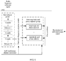
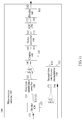
- FIG. 2 is a schematic structural diagram of an interference cancellation apparatus according to an embodiment of the present invention.
- an apparatus 100 provided by this embodiment includes: a main receive antenna 110, a divider 120, a first-type interference canceller 130, a coupler 140, a second-type interference reconstructor 150, a down converter 160, an ADC 170, and a divider 180, where: an output end of the main receive antenna 110 is connected to a first input end 131 of the first-type interference canceller 130; an input end 121 of the divider 120 is configured to acquire a radio frequency reference signal generated according to a transmit signal; a first output end 122 of the divider 120 is connected to a second input end 132 of the first-type interference canceller 130; an output end 133 of the first-type interference canceller 130 is connected to a first input end 141 of the coupler 140; a second output end 123 of the divider 120 is connected to a first input end 151 of the second-type interference reconstructor 150; a second input end of the main receive
- the main receive antenna 110 is configured to receive a radio frequency receive signal, and transmit the radio frequency receive signal to the first-type interference canceller 130.
- the divider 120 is configured to acquire a radio frequency reference signal generated according to a transmit signal, and transmit the radio frequency reference signal to the first-type interference canceller 130 and the second-type interference reconstructor 150.
- the first-type interference canceller 130 is configured to receive the radio frequency reference signal transmitted by the divider 120 and the radio frequency receive signal transmitted by the main receive antenna 110, and cancel a first-type self-interference component in the radio frequency receive signal according to the radio frequency reference signal to acquire a first processed signal, where the first-type self-interference component includes a main-path self-interference component.
- the second-type interference reconstructor 150 is configured to acquire the reconstructed self-interference signal according to a self-interference channel parameter and the radio frequency reference signal transmitted by the divider 120.
- the coupler 140 is configured to receive the first processed signal and the reconstructed self-interference signal transmitted by the second-type interference reconstructor 150, and cancel a second-type self-interference component in the first processed signal according to the reconstructed self-interference signal to generate a second processed signal.
- the down converter 160 is configured to perform down-conversion processing on the second processed signal to generate a third processed signal.
- the analog to digital converter ADC 170 is configured to perform analog to digital conversion on the third processed signal to generate a digital signal.
- the second-type interference reconstructor 150 is further configured to acquire a digital baseband reference signal, receive the digital signal generated by the analog to digital converter ADC 170 and the radio frequency reference signal transmitted by the divider 120, and perform self-interference channel estimation according to the digital baseband reference signal and the digital signal to acquire the self-interference channel parameter.
- FIG. 2 further shows that the divider 180 is configured to use the digital signal converted from the third processed signal as an output signal and as an input signal of the second-type interference reconstructor 150 separately.
- the main receive antenna 110 is configured to receive a radio signal, and input the received radio signal as a radio frequency receive signal to the first input end 131 of the first-type interference canceller 130, where the process of receiving a radio signal by the main receive antenna 110 may be similar to the process of receiving a radio signal by an antenna in the prior art, and is not further described herein for avoiding repetition.
- a coupler or a power divider may be used as the divider 120.
- a transmit signal after baseband processing may be used as a radio frequency reference signal, and input to the divider 120 through the input end 121 of the divider.
- the divider 120 can divide the radio frequency reference signal into two signals. One signal is transmitted to the second input end 132 of the first-type interference canceller 130 through the first output end 122 of the divider 120 and is received by the first-type interference canceller 130. The other signal is transmitted to the first input end 151 of the second-type interference reconstructor 150 through the second output end 123 of the divider 120 and is received by the second-type interference reconstructor 150.
- the coupler or power divider is used as the divider 120 in such a manner that waveforms of the two signals output from the divider 120 can be consistent with that of the radio frequency reference signal, which is good for subsequent interference cancellation based on the radio frequency reference signal.
- power of the two signals that the radio frequency reference signal is divided into may be the same or may be different, which is not particularly limited by the present invention.
- the process of transmitting the transmit signal after baseband processing may be similar to that in the prior art.
- the description of the process is omitted.
- the first-type interference canceller 130 may include a divider a, a combiner a, and a combiner b, where at least one transmission path constituted by at least one of a delayer, a phase adjuster, and an amplitude adjuster connected in series is included between the divider a and the combiner a, where an output end of the combiner a is connected to an input end of the combiner b.
- the first-type interference canceller 130 has two input ends.
- the divider a may be a power divider
- the combiner a and the combiner b may be couplers.
- the first input end 131 (namely, an input port of the combiner b) of the first-type interference canceller 130 is connected to the output end of the main receive antenna 110, and is configured to receive a signal (namely, a radio frequency receive signal) from the output end of the main receive antenna 110;
- the second input end 132 (namely, an input port of the divider a) of the first-type interference canceller 130 is connected to the first output end 122 of the divider 120, and is configured to receive one radio frequency reference signal from the divider 120.
- the first-type interference canceller 130 is specifically configured to perform, based on the radio frequency receive signal, delay processing, amplitude adjustment processing, and phase adjustment processing on the radio frequency reference signal, so that an amplitude of the radio frequency reference signal is in a direction opposite or approximately opposite to an amplitude of the first-type self-interference component in the radio frequency receive signal, and that a phase of the radio frequency reference signal is the same or approximately the same as a phase of the first-type self-interference component in the radio frequency receive signal; or perform, based on the radio frequency receive signal, delay processing, amplitude adjustment processing, and phase adjustment processing on the radio frequency reference signal, so that an amplitude of the radio frequency reference signal is the same or approximately the same as an amplitude of the first-type self-interference component in the radio frequency receive signal, and that a difference between a phase of the reference signal and a phase of the first-type self-interference component in the radio frequency receive signal is 180 degrees or approximately 180 degrees; and combine radio frequency reference signals obtained after delay processing, amplitude of
- the second input end 132 of the first-type interference canceller 130 is connected to the first output end 122 of the divider 120, and a signal (namely, a radio frequency reference signal) output from the first output end 122 of the divider 120 is input through the second input end 132 of the first-type interference canceller 130 to the divider a, where the divider a may be a power divider.
- the divider a divides the radio frequency reference signal into several radio frequency reference signals (power of the several radio frequency reference signals may be the same or different).
- an output end of the divider a outputs one radio frequency reference signal to an adjustment circuit constituted by a delayer, a phase adjuster, and an amplitude adjuster that are connected in series, where the adjustment circuit is configured to adjust a delay, an amplitude, and a phase of a signal by means of delaying, attenuation, phase shifting, and the like.
- the amplitude of the radio frequency reference signal may approach the amplitude of the first-type self-interference component (including a main-path self-interference component) in the radio frequency receive signal.
- the amplitudes are the same.
- the amplitudes may be adjusted to approximately the same.
- the difference between the phase of the radio frequency reference signal and the phase of the radio frequency receive signal (specifically, the first-type self-interference component in the radio frequency receive signal) may be adjusted to 180 degrees or approximately 180 degrees.
- the amplitude of the radio frequency reference signal may be in a direction opposite to the amplitude of the first-type self-interference component in the radio frequency receive signal.
- a best effect is that directions of the amplitudes are opposite.
- the amplitudes may be adjusted to be approximately opposite.
- the phase of the radio frequency reference signal may be adjusted to be the same or approximately the same as the phase of the radio frequency receive signal (specifically, the first-type self-interference component in the radio frequency receive signal).
- each tributary output by the divider may include at least one of a delayer, a phase adjuster, and an amplitude adjuster.
- the amplitude adjustment may be expressed as attenuation or gain, and only attenuation is used as an example for description in the foregoing embodiment.
- "approximately” may indicate that a similarity between two is within a preset range, where the preset range may be determined at random according to actual use and requirements, and is not particularly limited by the present invention. For avoiding repetition, the following omits descriptions of similarities unless otherwise specified.
- the combiner b may combine the radio frequency receive signal with the radio frequency reference signal obtained after the amplitude and phase adjustment and combination (for example, add the radio frequency reference signal to the radio frequency receive signal or subtract the radio frequency reference signal from the radio frequency receive signal), to cancel the first-type self-interference component in the radio frequency receive signal, thereby implementing first-type self-interference component cancellation processing for the radio frequency receive signal.
- the amplitude adjuster may be, for example, an attenuator.
- the phase adjuster may be, for example, a phase shifter.
- the delayer may be, for example, a delay line.
- the first processed signal output from the output end 133 (specifically, the output end of the combiner b) of the first-type interference canceller 130 is a signal generated by canceling the first-type self-interference component in the radio frequency receive signal.
- the delayer, phase adjuster, and amplitude adjuster may be adjusted in a manner of minimizing strength of the first processed signal output by the combiner b, based on the output of the combiner b.
- the present invention is not limited to the foregoing implementation manner, as long as strength of the radio frequency receive signal can be reduced according to the radio frequency reference signal (or strength of the first processed signal is less than strength of the radio frequency receive signal), an interference cancellation effect can be achieved.
- the second-type interference reconstructor 150 may include a self-interference estimation module 1501 and a self-interference signal reconstruction module 1502.
- the self-interference estimation module 1501 is configured to acquire the digital baseband reference signal, receive the digital signal generated by the analog to digital converter ADC 170, and perform self-interference channel estimation according to the digital baseband reference signal and the digital signal to acquire the self-interference channel parameter.
- the self-interference estimation module 1501 includes any one of a field-programmable gate array FPGA (Field-Programmable Gate Array), a central processing unit CPU (Central Processing Unit), and an application-specific integrated circuit ASIC (Application Specific Integrated Circuit).
- FPGA Field-Programmable Gate Array
- CPU Central Processing Unit
- ASIC Application Specific Integrated Circuit
- a pilot-based channel estimation method or an adaptive filtering method such as an LMS (Least mean square, least mean squares) algorithm or an RLS (Recursive least squares, recursive least squares) algorithm may be used, which pertains to the prior art and is not further described.
- the transmit signal includes a self-interference channel estimation timeslot and a data transmission timeslot that are disposed at an interval.
- full duplex data communication may be performed.
- a communications peer does not transmit data
- a signal received by a local receiver includes only a self-interference signal.
- the local end uses the self-interference channel estimation timeslot to perform self-interference channel estimation to acquire a self-interference channel parameter.
- the radio frequency receive signal includes only a second-type self-interference component.
- the self-interference channel estimation timeslot by referring to the digital baseband reference signal, self-interference channel estimation is performed on the digital signal that is acquired by processing the radio frequency receive signal. Therefore, in the self-interference channel estimation timeslot, the communications peer does not transmit a signal, and a signal received by the receiver includes only a self-interference signal. Because there is no signal from the communications peer, the receiver may perform self-interference channel estimation in the self-interference channel estimation timeslot to acquire a self-interference channel parameter, where the self-interference channel parameter may include parameters indicating a transmission path delay, a phase, and an amplitude of a second-type self-interference component.
- a signal received by the receiver includes a self-interference signal and a data signal
- the receiver may generate a reconstructed self-interference signal in the data transmission timeslot according to the radio frequency reference signal and the self-interference channel parameter, and use the reconstructed self-interference signal to cancel the second-type self-interference component.
- the self-interference signal reconstruction module 1502 is configured to receive the radio frequency reference signal transmitted by the divider 120 and the self-interference channel parameter acquired by the self-interference estimation module 1501, and acquire the reconstructed self-interference signal according to the self-interference channel parameter and the radio frequency reference signal.
- the self-interference signal reconstruction module 1502 includes: a first delayer group, a first amplitude and phase adjuster group, and a first combiner, where:
- the delayers in the first delayer group are connected by couplers, and that a delay signal of a radio frequency reference signal, formed in each delay, is output by a coupler. That is, an output end of a previous delayer is connected to an input end of the coupler, an output end of the coupler is connected to an amplitude and phase adjuster in the first amplitude and phase adjuster group, and another output end of the coupler is connected to an input end of a next delayer (the previous and next are only intended for clearly describing a sequence of transferring the radio frequency reference signal in the first delayer group, and not for limiting the implementation manner of the present invention).
- the first delayer group may include M delayers configured to delay the radio frequency reference signal for M times and form delay signals of M radio frequency reference signals. A quantity of delay taps that may be formed by the M delayers included in the first delayer group is M.
- the self-interference signal reconstruction module further includes: a first radio frequency selection switch, configured to receive the delay signal of the at least one radio frequency reference signal, select, from delay signals of all radio frequency reference signals, a delay signal of at least one radio frequency reference signal according to the self-interference channel parameter, and transmit the selected delay signal of the at least one radio frequency reference signal to the first amplitude and phase adjuster group.
- a first radio frequency selection switch configured to receive the delay signal of the at least one radio frequency reference signal, select, from delay signals of all radio frequency reference signals, a delay signal of at least one radio frequency reference signal according to the self-interference channel parameter, and transmit the selected delay signal of the at least one radio frequency reference signal to the first amplitude and phase adjuster group.
- the first radio frequency selection switch may be an M ⁇ K radio frequency selection switch. That is, in delay signals of the received M radio frequency reference signals, delay signals of K radio frequency reference signals may be selected from the delay signals of the M radio frequency reference signals according to the self-interference channel parameter and output.
- the self-interference signal reconstruction module 1502 includes: a second delayer group, a second amplitude and phase adjuster group, and a second combiner, where:
- a circulator includes three ports 1, 2, and 3.
- the first port 1 is configured to receive one radio frequency reference signal.
- the second port 2 of the circulator is configured to transmit the radio frequency reference signal received by the first port 1 to a delayer.
- the delayer performs delay processing on the radio frequency reference signal and then returns it to the second port 2.
- the circulator transmits the radio frequency reference signal obtained after delay processing to a next circulator through the third port 3.
- Delay lines may be used as delayers.
- the circulator receives the delay signal formed by the delayer, and transmits, through a coupler, a delay signal of the radio frequency reference signal, formed in each delay. That is, a third port 3 of a previous circulator is connected to an input end of a coupler, an output end of the coupler is connected to an amplitude and phase adjuster in the first amplitude and phase adjuster group, and another output end of the coupler is connected to a first port 1 of a next circulator (the previous and next are only intended for clearly describing a sequence of transferring the radio frequency reference signal in the first delayer group, and not for limiting the implementation manner of the present invention).
- the first delayer group may include M delayers configured to delay the radio frequency reference signal for M times and form delay signals of M radio frequency reference signals.
- a quantity of delay taps that may be formed by the M delayers included in the first delayer group is M.
- a delay line when a delay line is used as a delayer, a single end of the delay line is connected to a second port 2 of a circulator, that is, a delay signal is formed by transmitting the radio frequency reference signal in the delay line forward and then backward, and therefore, a half of a length of the delay line may be saved in comparison with the embodiment corresponding to FIG. 6 .
- the self-interference signal reconstruction module further includes: a second radio frequency selection switch, configured to receive the delay signal of the at least one radio frequency reference signal, select, from delay signals of all radio frequency reference signals, a delay signal of at least one radio frequency reference signal according to the self-interference channel parameter, and transmit the selected delay signal of the at least one radio frequency reference signal to the second amplitude and phase adjuster group.
- a second radio frequency selection switch configured to receive the delay signal of the at least one radio frequency reference signal, select, from delay signals of all radio frequency reference signals, a delay signal of at least one radio frequency reference signal according to the self-interference channel parameter, and transmit the selected delay signal of the at least one radio frequency reference signal to the second amplitude and phase adjuster group.
- the first radio frequency selection switch may be an M ⁇ K radio frequency selection switch. That is, in delay signals of the received M radio frequency reference signals, delay signals of K radio frequency reference signals may be selected from the delay signals of the M radio frequency reference signals according to the self-interference channel parameter and output.
- amplitude and phase adjuster may be implemented in the following manners.
- the amplitude and phase adjuster includes: an attenuator and a phase shifter, where:
- a delay generated by each delay tap may be set to T, that is, each delayer may form a delay T for one radio frequency reference signal.
- the coupler 140 is configured to receive the first processed signal generated by the first-type interference canceller 130 and the reconstructed self-interference signal transmitted by the second-type interference reconstructor 150, and cancel the second-type self-interference component in the first processed signal according to the reconstructed self-interference signal to generate the second processed signal.
- the down converter 160 is configured to perform down-conversion processing on the second processed signal transmitted by the coupler 140 to generate the third processed signal. Because the radio frequency receive signal is transmitted as a high frequency signal in a wireless transmission process, the down-conversion processing herein is to convert a high frequency signal component into a low frequency signal component, to avoid adverse impact of the high frequency signal component on self-interference channel estimation performed by the second-type interference reconstructor 150.
- the ADC 170 is configured to perform analog to digital conversion on the third processed signal transmitted by the down converter 160 to generate the digital signal.
- FIG. 2 further shows the divider 180, of which the structure and basic operating principle are the same as those of the divider 120.
- the divider 180 is configured to divide the digital signal transmitted by the ADC 170 into two digital signals, where one signal is used as an output signal, and the other signal is used as an input signal of the second-type interference reconstructor 150.
- the interference cancellation apparatus further includes a first amplifier 190, where the first amplifier 190 is disposed between the coupler 140 and the down converter 160 (in FIG. 10 , an LNA is used as an example of the first amplifier), and the first amplifier 190 is configured to amplify the second processed signal.
- the first amplifier amplifies the second processed signal, which may reduce a requirement of a transmitter side on power of a radio frequency transmit signal.
- the interference cancellation apparatus further includes:
- both the second amplifier and the third amplifier are LNAs.
- the second amplifier amplifies the first processed signal before noise reduction processing
- the third amplifier amplifies the radio frequency reference signal that enters the second-type interference reconstructor 150. In this way, a requirement on power of the radio frequency reference signal may be reduced, and the requirement of the transmitter side on the power of the radio frequency transmit signal is further reduced.
- a receive tributary corresponding to each receive antenna requires a near-field jammer corresponding to each transmit antenna, for reconstructing a reconstructed self-interference signal corresponding to each transmit tributary and canceling the first-type self-interference components one by one.
- MIMO Multiple Input Multiple Output
- interference cancellation processing is performed according to a radio frequency reference signal to cancel a first-type self-interference component in the radio frequency receive signal and acquire a first processed signal; and further, a reconstructed self-interference signal is acquired through self-interference channel estimation to cancel a second-type self-interference component in the first processed signal. Because the reconstructed self-interference signal is used directly in an analog domain to cancel the second-type self-interference component, a limitation by a dynamic range of an ADC/DAC can be avoided, and the second-type self-interference component can be canceled effectively.
- the interference cancellation apparatus according to the embodiment of the present invention is described in detail above with reference to FIG. 1 to FIG. 11 .
- the following describes in detail an interference cancellation method according to an embodiment of the present invention with reference to FIG. 12 .
- FIG. 12 shows a schematic flowchart of an interference cancellation method, where the method includes the following steps: 101. Acquire a radio frequency reference signal generated according to a transmit signal.
- a transmit signal after baseband processing may be used as a radio frequency reference signal, and input to, for example, a coupler or a power divider. Therefore, the radio frequency reference signal can be divided into two signals by the coupler or power divider, where one signal is used to generate a first processed signal and the other signal is used to generate a reconstructed self-interference signal.
- the acquiring a digital baseband reference signal may specifically include: acquiring the digital baseband reference signal by performing digital sampling on the radio frequency reference signal.
- the coupler or power divider is used to divide the radio frequency reference signal into two signals in such a manner that waveforms of the two signals can be consistent with that of the transmit signal, which is good for subsequent interference cancellation (including cancellation of the first-type self-interference component and cancellation of the second-type self-interference component) based on the radio frequency reference signal, where waveform consistency includes that the waveforms are the same as the waveform of the transmit signal or that a waveform similarity is within a preset range.
- the method further includes: amplifying the second processed signal.
- the method further includes: amplifying the first processed signal; and before the acquiring the reconstructed self-interference signal according to the self-interference channel parameter and the radio frequency reference signal in step 104, the method further includes: amplifying the radio frequency reference signal.
- the foregoing amplification of various signals is amplification performed by using a low noise amplifier (LNA).
- LNA low noise amplifier
- Directly amplifying the second processed signal may reduce a requirement of a transmitter side on power of a radio frequency transmit signal.
- separately amplifying the first processed signal and amplifying the radio frequency reference signal that enters the self-interference signal reconstruction module may also reduce a requirement on power of the radio frequency reference signal, and further reduce the requirement of the transmitter side on the power of the radio frequency transmit signal.
- the canceling a first-type self-interference component in the radio frequency receive signal according to the radio frequency reference signal, to generate a first processed signal in step 103 includes:
- an adjustment circuit constituted by a delayer, a phase adjuster, and an amplitude adjuster that are connected in series may be used for implementation. Therefore, in step 103, the amplitude and phase of the radio frequency reference signal may be adjusted by the adjustment circuit through delaying, phase shifting, attenuation, and the like. For example, through attenuation, the amplitude of the radio frequency reference signal may approach the amplitude of the first-type self-interference component in the radio frequency receive signal. Certainly, a best effect is that the amplitudes are the same. However, because an error exists in an actual application, the amplitudes may be adjusted to approximately the same. In addition, through phase shifting and/or delaying, the phase of the radio frequency reference signal may be adjusted to be opposite or approximately opposite to the phase of the first-type self-interference component (including a main-path interference signal) in the radio frequency receive signal.
- radio frequency reference signals after delay processing, and amplitude adjustment, and phase adjustment may be combined with (for example, added to) the radio frequency receive signal, to cancel the first-type self-interference component in the radio frequency receive signal.
- first-type self-interference component cancellation processing is implemented for the radio frequency receive signal, and the signal after the processing is used as the first processed signal.
- the amplitude adjuster may be, for example, an attenuator.
- the phase adjuster may be, for example, a phase shifter, and the delayer may be a delay line.
- the delayer, phase shifter, and attenuator may also be adjusted in a manner of minimizing strength of the first processed signal.
- the acquiring the reconstructed self-interference signal according to a self-interference channel parameter and the radio frequency reference signal in step 104 includes:
- the performing amplitude and phase adjustment on a delay signal of each radio frequency reference signal according to the self-interference channel parameter in step 104 may be implemented in the following manner:
- the transmit signal includes a self-interference channel estimation timeslot and a data transmission timeslot that are disposed at an interval.
- a communications peer does not transmit a signal
- a signal received by a receiver includes only a self-interference signal.
- the receiver may perform self-interference channel estimation in the self-interference channel estimation timeslot to acquire a self-interference channel parameter, where the self-interference channel parameter may include parameters indicating a transmission path delay, a phase, and an amplitude of a second-type self-interference component.
- a signal received by the receiver includes a self-interference signal and a data signal
- the receiver may generate a reconstructed self-interference signal in the data transmission timeslot according to the radio frequency reference signal and the self-interference channel parameter, and use the reconstructed self-interference signal to cancel the second-type self-interference component.
- interference cancellation processing is performed according to a radio frequency reference signal to cancel a first-type self-interference component in the radio frequency receive signal and acquire a first processed signal; and further, a reconstructed self-interference signal is acquired through self-interference channel estimation to cancel a second-type self-interference component in the first processed signal. Because the reconstructed self-interference signal is used directly in an analog domain to cancel the second-type self-interference component, a limitation by a dynamic range of an ADC/DAC can be avoided, and the second-type self-interference component can be canceled effectively.
- sequence numbers of the foregoing processes do not mean execution sequences in various embodiments of the present invention.
- the execution sequences of the processes should be determined according to functions and internal logic of the processes, and should not be construed as any limitation on the implementation processes of the embodiments of the present invention.
- the disclosed apparatus may be implemented in other manners.
- the described apparatus embodiment is merely exemplary.
- the unit division is merely logical function division and may be other division in actual implementation.
- a plurality of units or components may be combined or integrated into another system, or some features may be ignored or not performed.
- the displayed or discussed mutual couplings or direct couplings or communication connections may be implemented through some interfaces.
- the indirect couplings or communication connections between the apparatuses or units may be implemented in electronic, mechanical, or other forms.
- the units described as separate parts may or may not be physically separate, and parts displayed as units may or may not be physical units, may be located in one position, or may be distributed on a plurality of network units. Some or all of the units may be selected according to actual needs to achieve the objectives of the solutions of the embodiments.
- functional units in the embodiments of the present invention may be integrated into one processing unit, or each of the units may exist alone physically, or two or more units are integrated into one unit.
- the functions When the functions are implemented in the form of a software functional unit and sold or used as an independent product, the functions may be stored in a computer-readable storage medium. Based on such an understanding, the technical solutions of the present invention essentially, or the part contributing to the prior art, or some of the technical solutions may be implemented in a form of a software product.
- the computer software product is stored in a storage medium, and includes several instructions for instructing a computer device (which may be a personal computer, a server, or a network device) to perform all or some of the steps of the methods described in the embodiments of the present invention.
- the foregoing storage medium includes: any medium that can store program code, such as a USB flash drive, a removable hard disk, a read-only memory (ROM, Read-Only Memory), a random access memory (RAM, Random Access Memory), a magnetic disk, or an optical disc.
- program code such as a USB flash drive, a removable hard disk, a read-only memory (ROM, Read-Only Memory), a random access memory (RAM, Random Access Memory), a magnetic disk, or an optical disc.
Landscapes
- Engineering & Computer Science (AREA)
- Computer Networks & Wireless Communication (AREA)
- Signal Processing (AREA)
- Noise Elimination (AREA)
- Mobile Radio Communication Systems (AREA)
- Cable Transmission Systems, Equalization Of Radio And Reduction Of Echo (AREA)
Claims (18)
- Appareil de suppression de brouillage, comprenant :une antenne de réception principale (110), configurée pour recevoir un signal de réception radiofréquence, et transmettre le signal de réception radiofréquence à un suppresseur de brouillage de premier type (130) ;un diviseur (120), configuré pour acquérir un signal de référence radiofréquence généré conformément à un signal d'émission, et transmettre le signal de référence radiofréquence au suppresseur de brouillage de premier type (130) et à un reconstructeur de brouillage de second type (150) ;le suppresseur de brouillage de premier type (130) étant configuré pour recevoir le signal de référence radiofréquence transmis par le diviseur (120) et le signal de réception radiofréquence transmis par l'antenne de réception principale (110), et supprimer une composante d'auto-brouillage de premier type dans le signal de réception radiofréquence conformément au signal de référence radiofréquence afin de générer un premier signal traité, la composante d'auto-brouillage de premier type comprenant une composante d'auto-brouillage sur chemin principal ;le reconstructeur de brouillage de second type (150) étant configuré pour générer un signal d'auto-brouillage reconstruit conformément à un paramètre de canal d'auto-brouillage et au signal de référence radiofréquence transmis par le diviseur (120) ;un coupleur (140), configuré pour recevoir le premier signal traité et le signal d'auto-brouillage reconstruit transmis par le reconstructeur de brouillage de second type (150), et supprimer une composante d'auto-brouillage de second type dans le premier signal traité conformément au signal d'auto-brouillage reconstruit afin de générer un deuxième signal traité ;un convertisseur abaisseur (160), configuré pour effectuer un traitement de conversion par abaissement sur le deuxième signal traité afin de générer un troisième signal traité ; etun convertisseur analogique/numérique ADC (170), configuré pour effectuer une conversion analogique/numérique sur le troisième signal traité afin de générer un signal numérique ; dans lequelle reconstructeur de brouillage de second type (150) est configuré en outre pour acquérir un signal de référence en bande de base numérique, recevoir le signal numérique généré par le convertisseur analogique/numérique ADC (170) et le signal de référence radiofréquence transmis par le diviseur (120), et effectuer une estimation de canal d'auto-brouillage conformément au signal de référence en bande de base numérique et au signal numérique afin de générer le paramètre de canal d'auto-brouillage.
- Appareil selon la revendication 1, dans lequel le reconstructeur de brouillage de second type (150) comprend :un module d'estimation d'auto-brouillage (1501), configuré pour acquérir le signal de référence en bande de base numérique, recevoir le signal numérique généré par le convertisseur analogique/numérique ADC (170), et effectuer une estimation de canal d'auto-brouillage conformément au signal de référence en bande de base numérique et au signal numérique afin de générer le paramètre de canal d'auto-brouillage ; etun module de reconstruction de signal d'auto-brouillage (1502), configuré pour recevoir le signal de référence radiofréquence transmis par le diviseur (120) et le paramètre de canal d'auto-brouillage généré par le module d'estimation d'auto-brouillage (1501), et générer le signal d'auto-brouillage reconstruit conformément au paramètre de canal d'auto-brouillage et au signal de référence radiofréquence.
- Appareil selon la revendication 1, comprenant en outre un premier amplificateur, le premier amplificateur étant configuré pour amplifier le deuxième signal traité.
- Appareil selon la revendication 1, comprenant en outre un deuxième amplificateur et un troisième amplificateur, dans lequel :le deuxième amplificateur est configuré pour amplifier le premier signal traité ; etle troisième amplificateur est configuré pour amplifier le signal de référence radiofréquence reçu par le reconstructeur de brouillage de second type.
- Appareil selon la revendication 2, dans lequel le module de reconstruction de signal d'auto-brouillage (1502) comprend :
un premier groupe de circuits de retard, un premier groupe de circuits de réglage d'amplitude et de phase, et un premier combineur, dans lequel :le premier groupe de circuits de retard comprend au moins un circuit de retard, dans lequel l'au moins un circuit de retard est connecté en série, et le premier groupe de circuits de retard est configuré pour recevoir le signal de référence radiofréquence, et effectuer un traitement de retard sur le signal de référence radiofréquence en utilisant l'au moins un circuit de retard séquentiellement, afin de former un signal retardé d'au moins un signal de référence radiofréquence ;le premier groupe de circuits de réglage d'amplitude et de phase comprend au moins un circuit de réglage d'amplitude et de phase, dans lequel chaque circuit de réglage d'amplitude et de phase est configuré pour effectuer un réglage d'amplitude et de phase sur un signal retardé d'un signal de référence radiofréquence conformément au paramètre de canal d'auto-brouillage ; etle premier combineur est configuré pour effectuer un traitement de combinaison sur des signaux retardés de signaux de référence radiofréquence qui sont obtenus après un réglage d'amplitude et de phase, afin de générer le signal d'auto-brouillage reconstruit. - Appareil selon la revendication 5, dans lequel le module de reconstruction de signal d'auto-brouillage (1502) comprend en outre :
un premier commutateur de sélection radiofréquence configuré pour recevoir le signal retardé de l'au moins un signal de référence radiofréquence, sélectionner, parmi des signaux retardés de tous les signaux de référence radiofréquence, un signal retardé d'au moins un signal de référence radiofréquence conformément au paramètre de canal d'auto-brouillage, et transmettre le signal retardé sélectionné de l'au moins un signal de référence radiofréquence au premier groupe de circuits de réglage d'amplitude et de phase. - Appareil selon la revendication 2, dans lequel le module de reconstruction de signal d'auto-brouillage (1502) comprend :
un second groupe de circuits de retard, un second groupe de circuits de réglage d'amplitude et de phase, et un second combineur, dans lequel :le second groupe de circuits de retard comprend au moins un circulateur et au moins un circuit de retard, dans lequel l'au moins un circulateur est connecté en série en utilisant un premier port et un troisième port, et une extrémité du circuit de retard est connectée à un second port du circulateur ; le premier groupe de circuits de retard est configuré pour recevoir le signal de référence radiofréquence, et effecteur un traitement de retard sur le signal de référence radiofréquence en utilisant l'au moins un circuit de retard séquentiellement, afin de former un signal retardé d'au moins un signal de référence radiofréquence ;le second groupe de circuits de réglage d'amplitude et de phase comprend au moins un circuit de réglage d'amplitude et de phase, dans lequel chaque circuit de réglage d'amplitude et de phase est configuré pour effectuer un réglage d'amplitude et de phase sur un signal retardé d'un signal de référence radiofréquence conformément au paramètre de canal d'auto-brouillage ; etle second combineur est configuré pour effectuer un traitement de combinaison sur des signaux retardés de signaux de référence radiofréquence qui sont obtenus après un réglage d'amplitude et de phase, afin de générer le signal d'auto-brouillage reconstruit. - Appareil selon la revendication 7, dans lequel le module de reconstruction de signal d'auto-brouillage (1502) comprend en outre :
un second commutateur de sélection radiofréquence configuré pour recevoir le signal retardé de l'au moins un signal de référence radiofréquence, sélectionner, parmi des signaux retardés de tous les signaux de référence radiofréquence, un signal retardé d'au moins un signal de référence radiofréquence conformément au paramètre de canal d'auto-brouillage, et transmettre le signal retardé sélectionné de l'au moins un signal de référence radiofréquence au second groupe de circuits de réglage d'amplitude et de phase. - Appareil selon l'une quelconque des revendications 5 à 8, dans lequel le circuit de réglage d'amplitude et de phase comprend un atténuateur et un déphaseur, dans lequel :l'atténuateur est configuré pour effectuer, conformément au paramètre de canal d'auto-brouillage, un traitement de réglage d'amplitude sur le signal retardé reçu du signal de référence radiofréquence et transmis par le commutateur de sélection radiofréquence ; etle déphaseur est configuré pour effectuer, conformément au paramètre de canal d'auto-brouillage, un traitement de déphasage sur un signal retardé du signal de référence radiofréquence qui est obtenu après le traitement de réglage d'amplitude effectué par l'atténuateur.
- Appareil selon l'une quelconque des revendications 1 à 9, dans lequel :le suppresseur de brouillage de premier type (130) est configuré spécifiquement pour effectuer, en fonction du signal de réception radiofréquence, un traitement de retard, un traitement de réglage d'amplitude, et un traitement de réglage de phase sur le signal de référence radiofréquence, de telle sorte qu'une amplitude du signal de référence radiofréquence soit de sens opposé ou approximativement opposé à une amplitude de la composante d'auto-brouillage de premier type dans le signal de réception radiofréquence, et qu'une phase du signal de référence radiofréquence soit identique ou approximativement identique à une phase de la composante d'auto-brouillage de premier type dans le signal de réception radiofréquence ; oueffectuer, en fonction du signal de réception radiofréquence, un traitement de retard, un traitement de réglage d'amplitude, et un traitement de réglage de phase sur le signal de référence radiofréquence, de telle sorte qu'une amplitude du signal de référence radiofréquence soit identique ou approximativement identique à une amplitude de la composante d'auto-brouillage de premier type dans le signal de réception radiofréquence, et qu'une différence entre une phase du signal de référence radiofréquence et une phase de la composante d'auto-brouillage de premier type dans le signal de réception radiofréquence soit 180 degrés ou approximativement 180 degrés.
- Appareil selon la revendication 2, dans lequel le module d'estimation d'auto-brouillage (1501) comprend un réseau prédiffusé programmable par l'utilisateur FPGA, une unité centrale de traitement CPU, ou un circuit intégré spécifique à l'application ASIC.
- Procédé de suppression de brouillage, comprenant :l'acquisition d'un signal de référence radiofréquence généré conformément à un signal d'émission ;la réception d'un signal de réception radiofréquence à l'aide d'une antenne de réception principale ;la suppression d'une composante d'auto-brouillage de premier type dans le signal de réception radiofréquence conformément au signal de référence radiofréquence, afin de générer un premier signal traité, la composante d'auto-brouillage de premier type comprenant une composante d'auto-brouillage sur chemin principal ;la génération du signal d'auto-brouillage reconstruit conformément à un paramètre de canal d'auto-brouillage et au signal de référence radiofréquence ;la suppression d'une composante d'auto-brouillage de second type dans le premier signal traité conformément au signal d'auto-brouillage reconstruit afin de générer un deuxième signal traité ;l'exécution d'un traitement de conversion par abaissement sur le deuxième signal traité afin de générer un troisième signal traité ;l'exécution d'une conversion analogique/numérique sur le troisième signal traité afin de générer un signal numérique ; etl'acquisition d'un signal de référence en bande de base numérique, et l'exécution d'une estimation de canal d'auto-brouillage conformément au signal de référence en bande de base numérique et au signal numérique afin de générer le paramètre de canal d'auto-brouillage.
- Procédé selon la revendication 12, le procédé comprenant en outre : l'amplification du deuxième signal traité.
- Procédé selon la revendication 12, le procédé comprenant en outre :l'amplification du premier signal traité ; etle procédé comprenant, avant la génération du signal d'auto-brouillage reconstruit conformément au paramètre de canal d'auto-brouillage et au signal de référence radiofréquence : l'amplification du signal de référence radiofréquence.
- Procédé selon la revendication 12, dans lequel la génération du signal d'auto-brouillage reconstruit conformément à un paramètre de canal d'auto-brouillage et au signal de référence radiofréquence comprend :l'exécution d'un traitement de retard sur le signal de référence radiofréquence pendant au moins une durée, afin de former un signal retardé d'au moins un signal de référence radiofréquence ;l'exécution d'un réglage d'amplitude et de phase sur un signal retardé de chaque signal de référence radiofréquence conformément au paramètre de canal d'auto-brouillage ; etl'exécution d'un traitement de combinaison sur des signaux retardés de signaux de référence radiofréquence qui sont obtenus après un réglage d'amplitude et de phase, afin de générer le signal d'auto-brouillage reconstruit.
- Procédé selon la revendication 15, le procédé comprenant en outre, avant l'exécution d'un réglage d'amplitude et de phase sur un signal retardé de chaque signal de référence radiofréquence conformément au paramètre de canal d'auto-brouillage :la sélection, parmi des signaux retardés de tous les signaux de référence radiofréquence, d'un signal retardé d'au moins un signal de référence radiofréquence conformément au paramètre de canal d'auto-brouillage ; etl'exécution d'un réglage d'amplitude et de phase sur un signal retardé de chaque signal de référence radiofréquence conformément au paramètre de canal d'auto-brouillage consiste spécifiquement en : l'exécution d'un réglage d'amplitude et de phase sur le signal retardé de chaque signal de référence radiofréquence dans le signal retardé sélectionné de l'au moins un signal de référence radiofréquence.
- Procédé selon la revendication 15, dans lequel l'exécution d'un réglage d'amplitude et de phase sur un signal retardé de chaque signal de référence radiofréquence conformément au paramètre de canal d'auto-brouillage comprend :l'exécution d'un traitement de réglage d'amplitude sur le signal retardé du signal de référence radiofréquence conformément au paramètre de canal d'auto-brouillage ; etl'exécution, conformément au paramètre de canal d'auto-brouillage, d'un traitement de déphasage sur un signal retardé du signal de référence radiofréquence obtenu après l'exécution d'un traitement de réglage d'amplitude.
- Procédé selon l'une quelconque des revendications 12 à 17, dans lequel la suppression d'une composante d'auto-brouillage de premier type dans le signal de réception radiofréquence conformément au signal de référence radiofréquence comprend :l'exécution, en fonction du signal de réception radiofréquence, d'un traitement de retard, d'un traitement de réglage d'amplitude, et d'un traitement de réglage de phase sur le signal de référence radiofréquence, de telle sorte qu'une amplitude du signal de référence radiofréquence soit de sens opposé ou approximativement opposé à une amplitude de la composante d'auto-brouillage de premier type dans le signal de réception radiofréquence, et qu'une phase du signal de référence radiofréquence soit identique ou approximativement identique à une phase de la composante d'auto-brouillage de premier type dans le signal de réception radiofréquence ; oul'exécution, en fonction du signal de réception radiofréquence, d'un traitement de retard, d'un traitement de réglage d'amplitude, et d'un traitement de réglage de phase sur le signal de référence radiofréquence, de telle sorte qu'une amplitude du signal de référence radiofréquence soit identique ou approximativement identique à une amplitude de la composante d'auto-brouillage de premier type dans le signal de réception radiofréquence, et qu'une différence entre une phase du signal de référence radiofréquence et une phase de la composante d'auto-brouillage de premier type dans le signal de réception radiofréquence soit 180 degrés ou approximativement 180 degrés.
Applications Claiming Priority (1)
| Application Number | Priority Date | Filing Date | Title |
|---|---|---|---|
| PCT/CN2014/080870 WO2015196428A1 (fr) | 2014-06-26 | 2014-06-26 | Dispositif et procédé d'annulation d'interférences |
Publications (3)
| Publication Number | Publication Date |
|---|---|
| EP3151438A1 EP3151438A1 (fr) | 2017-04-05 |
| EP3151438A4 EP3151438A4 (fr) | 2017-07-12 |
| EP3151438B1 true EP3151438B1 (fr) | 2019-04-10 |
Family
ID=54936490
Family Applications (1)
| Application Number | Title | Priority Date | Filing Date |
|---|---|---|---|
| EP14895760.8A Active EP3151438B1 (fr) | 2014-06-26 | 2014-06-26 | Dispositif et procédé d'annulation d'interférences |
Country Status (12)
| Country | Link |
|---|---|
| US (1) | US9973224B2 (fr) |
| EP (1) | EP3151438B1 (fr) |
| JP (1) | JP6562566B2 (fr) |
| KR (1) | KR101901220B1 (fr) |
| CN (1) | CN106464284B (fr) |
| AU (1) | AU2014399209B2 (fr) |
| BR (1) | BR112016030506B1 (fr) |
| CA (1) | CA2953658C (fr) |
| MX (1) | MX360550B (fr) |
| RU (1) | RU2664392C2 (fr) |
| SG (1) | SG11201610769YA (fr) |
| WO (1) | WO2015196428A1 (fr) |
Families Citing this family (39)
| Publication number | Priority date | Publication date | Assignee | Title |
|---|---|---|---|---|
| US9001920B2 (en) * | 2013-02-19 | 2015-04-07 | At&T Intellectual Property I, Lp | Apparatus and method for interference cancellation in communication systems |
| KR102222353B1 (ko) | 2013-08-09 | 2021-03-03 | 쿠무 네트웍스, 아이엔씨. | 비선형 디지털 자기 간섭 제거를 위한 시스템 및 방법 |
| CN105359473B (zh) * | 2013-10-17 | 2018-11-06 | 华为技术有限公司 | 一种信道估计方法、装置及系统 |
| AU2014399206B2 (en) * | 2014-06-26 | 2017-08-31 | Huawei Technologies Co., Ltd. | Interference cancellation apparatus and method |
| CA2953658C (fr) | 2014-06-26 | 2020-05-12 | Huawei Technologies Co., Ltd. | Dispositif et procede d'annulation d'interferences |
| WO2015196404A1 (fr) | 2014-06-26 | 2015-12-30 | 华为技术有限公司 | Dispositif et procédé d'annulation d'interférence |
| PL226101B1 (pl) * | 2015-02-10 | 2017-06-30 | Sławomir Szechniuk | Sposob redukcji zaklocen i szumow w ukladach z dwoma torami sygnalow oraz filtr fazowy |
| US10033542B2 (en) | 2015-07-15 | 2018-07-24 | Cisco Technology, Inc. | Scheduling mechanisms in full duplex cable network environments |
| US9966993B2 (en) * | 2015-07-15 | 2018-05-08 | Cisco Technology, Inc. | Interference suppression in full duplex cable network environments |
| US9912464B2 (en) | 2015-07-15 | 2018-03-06 | Cisco Technology, Inc. | Interference relationship characterization in full duplex cable network environments |
| US9942024B2 (en) | 2015-07-15 | 2018-04-10 | Cisco Technology, Inc. | Full duplex network architecture in cable network environments |
| US10230423B2 (en) * | 2015-11-10 | 2019-03-12 | Huawei Technologies Canada Co., Ltd. | System and method for balanced passive cancellation for full duplex communications |
| US9742593B2 (en) | 2015-12-16 | 2017-08-22 | Kumu Networks, Inc. | Systems and methods for adaptively-tuned digital self-interference cancellation |
| US10797750B2 (en) | 2016-02-24 | 2020-10-06 | Cisco Technology, Inc. | System architecture for supporting digital pre-distortion and full duplex in cable network environments |
| EP3440779A1 (fr) * | 2016-04-05 | 2019-02-13 | Telefonaktiebolaget LM Ericsson (publ) | Suppression d'interférence dans un dispositif émetteur-récepteur radio |
| CN107276599B (zh) * | 2016-04-07 | 2021-05-04 | 中兴通讯股份有限公司 | 抗干扰方法、电路及移动终端 |
| US10389510B2 (en) * | 2016-07-22 | 2019-08-20 | Electronics And Telecommunications Research Institute | Self-interference signal cancellation apparatus and transceiver including the same |
| TW201820796A (zh) * | 2016-11-17 | 2018-06-01 | 財團法人資訊工業策進會 | 針對全雙工通訊裝置的自干擾消除訊號產生裝置與方法 |
| US10103774B1 (en) | 2017-03-27 | 2018-10-16 | Kumu Networks, Inc. | Systems and methods for intelligently-tuned digital self-interference cancellation |
| CN111052642B (zh) | 2017-06-06 | 2023-12-26 | 弗劳恩霍夫应用研究促进协会 | 射频通信和干扰设备及相应的方法 |
| EP3627724A4 (fr) * | 2017-06-26 | 2020-06-17 | Guangdong Oppo Mobile Telecommunications Corp., Ltd. | Procédé et dispositif de communication sans fil |
| CN107359896B (zh) * | 2017-06-27 | 2019-06-07 | 电子科技大学 | 一种三维区域内电磁波设备的干扰抑制系统及方法 |
| CN107547105B (zh) * | 2017-08-31 | 2019-10-18 | 电子科技大学 | 一种用于抵消不可分辨多径的全双工射频自干扰抑制方法 |
| EP3499731B1 (fr) * | 2017-12-18 | 2021-07-14 | NXP USA, Inc. | Appareil et procédé d'annulation de signaux d'interférence |
| US10425115B2 (en) | 2018-02-27 | 2019-09-24 | Kumu Networks, Inc. | Systems and methods for configurable hybrid self-interference cancellation |
| KR102503541B1 (ko) | 2018-09-04 | 2023-02-27 | 삼성전자주식회사 | 데이터 통신 신호로부터 무선 전력에 의한 간섭을 제거하는 전자 장치 및 그 작동 방법 |
| KR20200071491A (ko) * | 2018-12-11 | 2020-06-19 | 삼성전자주식회사 | 안테나를 통해 수신된 신호의 적어도 일부를 감쇄하기 위한 전자 장치 및 통신 신호 제어 방법 |
| US10868661B2 (en) | 2019-03-14 | 2020-12-15 | Kumu Networks, Inc. | Systems and methods for efficiently-transformed digital self-interference cancellation |
| CN111865361B (zh) * | 2019-04-25 | 2023-03-24 | 华为技术有限公司 | 一种全双工自干扰消除方法和装置 |
| US11159197B2 (en) * | 2019-04-29 | 2021-10-26 | Qualcomm Incorporated | Self-interference cancellation for in-band full-duplex wireless communication |
| JP7269144B2 (ja) * | 2019-10-07 | 2023-05-08 | 株式会社東芝 | レーダ装置、信号処理装置、および方法 |
| US11245430B1 (en) * | 2020-08-14 | 2022-02-08 | Apple Inc. | Wireless transmitters having self-interference cancellation circuitry |
| CN111948614B (zh) * | 2020-08-20 | 2023-01-10 | 电子科技大学 | 一种相控阵雷达宽带自干扰射频域分段对消系统及方法 |
| CN112235073B (zh) * | 2020-10-22 | 2023-09-01 | 维沃移动通信有限公司 | 干扰信号的抵消方法、驱动集成电路和电子设备 |
| US11726166B2 (en) * | 2020-11-18 | 2023-08-15 | Kabushiki Kaislia Toshiba | Dual polar full duplex radar transceiver |
| CN114726459B (zh) * | 2021-01-04 | 2024-09-06 | 中国移动通信有限公司研究院 | 一种干扰消除方法、装置及设备 |
| CN113206677B (zh) * | 2021-04-28 | 2022-09-27 | 中国电子科技集团公司第三十六研究所 | 一种自干扰抵消器 |
| CN115276686B (zh) * | 2022-06-22 | 2024-03-01 | 中国科学院国家天文台 | 低频射电频谱仪干扰信号的处理方法、装置、设备及介质 |
| CN116112324B (zh) * | 2023-02-02 | 2024-10-15 | 电子科技大学 | 一种同时同频自干扰收发联合抑制方法 |
Family Cites Families (40)
| Publication number | Priority date | Publication date | Assignee | Title |
|---|---|---|---|---|
| GB9423027D0 (en) | 1994-11-15 | 1995-01-04 | Univ Bristol | Full-duplex radio transmitter/receiver |
| US5691978A (en) * | 1995-04-07 | 1997-11-25 | Signal Science, Inc. | Self-cancelling full-duplex RF communication system |
| JP3603714B2 (ja) * | 2000-01-06 | 2004-12-22 | Kddi株式会社 | 符号分割多元接続方式用リピータ装置 |
| US20030098806A1 (en) * | 2001-11-27 | 2003-05-29 | Green Evan R. | Rejecting interference for simultaneous received signals |
| CN1553601A (zh) * | 2003-06-03 | 2004-12-08 | 西门子(中国)有限公司 | 时分双工系统中消除自生干扰的方法 |
| US7804760B2 (en) * | 2003-08-07 | 2010-09-28 | Quellan, Inc. | Method and system for signal emulation |
| US7123676B2 (en) * | 2003-11-17 | 2006-10-17 | Quellan, Inc. | Method and system for antenna interference cancellation |
| JP2008017341A (ja) * | 2006-07-07 | 2008-01-24 | Ntt Docomo Inc | 無線通信装置および無線通信方法 |
| EP2095516A2 (fr) | 2006-11-06 | 2009-09-02 | Nokia Corporation | Modélisation de trajet de signal analogique pour annulation d'autobrouillage |
| CN101453228B (zh) * | 2007-12-04 | 2013-04-17 | 松下电器产业株式会社 | 共站址干扰消除系统和方法 |
| US8526903B2 (en) | 2008-03-11 | 2013-09-03 | Qualcomm, Incorporated | High-linearity receiver with transmit leakage cancellation |
| US8249540B1 (en) * | 2008-08-07 | 2012-08-21 | Hypres, Inc. | Two stage radio frequency interference cancellation system and method |
| CN101656562B (zh) * | 2009-09-22 | 2012-07-18 | 武汉虹信通信技术有限责任公司 | 一种实现直放站自激干扰消除的装置及方法 |
| KR101386839B1 (ko) | 2010-05-18 | 2014-04-18 | 엘에스산전 주식회사 | Rfid 시스템의 송신누설신호 제거장치 |
| US8630211B2 (en) | 2010-06-30 | 2014-01-14 | Qualcomm Incorporated | Hybrid radio architecture for repeaters using RF cancellation reference |
| US10284356B2 (en) * | 2011-02-03 | 2019-05-07 | The Board Of Trustees Of The Leland Stanford Junior University | Self-interference cancellation |
| US9019849B2 (en) * | 2011-11-07 | 2015-04-28 | Telefonaktiebolaget L M Ericsson (Publ) | Dynamic space division duplex (SDD) wireless communications with multiple antennas using self-interference cancellation |
| US10243719B2 (en) * | 2011-11-09 | 2019-03-26 | The Board Of Trustees Of The Leland Stanford Junior University | Self-interference cancellation for MIMO radios |
| WO2015048678A1 (fr) | 2013-09-27 | 2015-04-02 | The Board Of Trustees Of The Leland Stanford Junior University | Annulation d'auto-interférences pour des radios mimo |
| CN103139115B (zh) | 2011-11-25 | 2016-08-03 | 华为技术有限公司 | 一种干扰对齐方法、装置及系统 |
| KR101342760B1 (ko) * | 2011-12-01 | 2013-12-19 | 연세대학교 산학협력단 | 노드, 릴레이 노드 및 이의 제어 방법 |
| CN103200140B (zh) | 2012-01-06 | 2016-05-11 | 微思泰(北京)信息技术有限公司 | 一种基于预均衡的干扰消除系统及方法 |
| EP2850741B1 (fr) | 2012-05-13 | 2019-05-01 | Amir Khandani | Signalisation collaborative répartie dans des émetteurs-récepteurs sans fil bilatéraux simultanés |
| US8842584B2 (en) | 2012-07-13 | 2014-09-23 | At&T Intellectual Property I, L.P. | System and method for full duplex cancellation |
| CN103595520B (zh) | 2012-08-16 | 2017-08-04 | 华为技术有限公司 | 通讯装置及其空分双工方法 |
| CN103685098B (zh) | 2012-09-07 | 2017-04-12 | 华为技术有限公司 | 一种干扰信号的处理方法、装置和系统 |
| WO2014061443A1 (fr) | 2012-10-17 | 2014-04-24 | 株式会社村田製作所 | Dispositif émetteur/récepteur |
| US8964608B2 (en) | 2013-01-11 | 2015-02-24 | Futurewei Technologies, Inc. | Interference cancellation for division free duplexing or full duplex operation |
| CN103297069B (zh) | 2013-05-08 | 2015-05-20 | 北京工业大学 | 一种全双工无线电射频干扰删除装置与方法 |
| US9100110B2 (en) * | 2013-08-29 | 2015-08-04 | Qualcomm Incorporated | Non-linear interference cancellation with multiple aggressors |
| CN103427872B (zh) * | 2013-09-03 | 2015-01-21 | 电子科技大学 | 一种同时同频全双工多抽头射频自干扰抵消系统及方法 |
| CN103427874B (zh) * | 2013-09-03 | 2015-03-11 | 电子科技大学 | 多径环境下大发射功率同时同频自干扰抵消系统及方法 |
| CN103580720B (zh) | 2013-11-20 | 2015-07-08 | 东南大学 | 一种同频全双工自干扰抵消装置 |
| WO2015078009A1 (fr) | 2013-11-29 | 2015-06-04 | 华为技术有限公司 | Procédé et dispositif permettant d'affaiblir un signal d'autobrouillage dans un système de communication |
| CN105474549B (zh) * | 2013-12-04 | 2018-05-11 | 华为技术有限公司 | 收发共用天线的自干扰消除方法、收发机和通信设备 |
| CN103701480A (zh) | 2013-12-31 | 2014-04-02 | 上海交通大学 | 无线全双工单输入单输出通信模拟自干扰信号消除装置 |
| WO2015139266A1 (fr) * | 2014-03-20 | 2015-09-24 | 华为技术有限公司 | Appareil et procédé d'annulation d'auto-interférence |
| WO2015196404A1 (fr) | 2014-06-26 | 2015-12-30 | 华为技术有限公司 | Dispositif et procédé d'annulation d'interférence |
| AU2014399206B2 (en) | 2014-06-26 | 2017-08-31 | Huawei Technologies Co., Ltd. | Interference cancellation apparatus and method |
| CA2953658C (fr) | 2014-06-26 | 2020-05-12 | Huawei Technologies Co., Ltd. | Dispositif et procede d'annulation d'interferences |
-
2014
- 2014-06-26 CA CA2953658A patent/CA2953658C/fr active Active
- 2014-06-26 MX MX2016017327A patent/MX360550B/es active IP Right Grant
- 2014-06-26 WO PCT/CN2014/080870 patent/WO2015196428A1/fr active Application Filing
- 2014-06-26 EP EP14895760.8A patent/EP3151438B1/fr active Active
- 2014-06-26 JP JP2016574975A patent/JP6562566B2/ja active Active
- 2014-06-26 BR BR112016030506-0A patent/BR112016030506B1/pt active IP Right Grant
- 2014-06-26 KR KR1020177001698A patent/KR101901220B1/ko active IP Right Grant
- 2014-06-26 SG SG11201610769YA patent/SG11201610769YA/en unknown
- 2014-06-26 AU AU2014399209A patent/AU2014399209B2/en active Active
- 2014-06-26 RU RU2017102384A patent/RU2664392C2/ru active
- 2014-06-26 CN CN201480079679.6A patent/CN106464284B/zh active Active
-
2016
- 2016-12-22 US US15/388,968 patent/US9973224B2/en active Active
Non-Patent Citations (1)
| Title |
|---|
| None * |
Also Published As
| Publication number | Publication date |
|---|---|
| MX2016017327A (es) | 2017-07-07 |
| CN106464284B (zh) | 2019-08-16 |
| RU2017102384A (ru) | 2018-08-02 |
| AU2014399209A1 (en) | 2017-02-02 |
| SG11201610769YA (en) | 2017-01-27 |
| AU2014399209B2 (en) | 2018-03-29 |
| JP6562566B2 (ja) | 2019-08-21 |
| BR112016030506A2 (fr) | 2017-08-22 |
| US9973224B2 (en) | 2018-05-15 |
| RU2017102384A3 (fr) | 2018-08-02 |
| CN106464284A (zh) | 2017-02-22 |
| KR101901220B1 (ko) | 2018-09-21 |
| JP2017520192A (ja) | 2017-07-20 |
| CA2953658C (fr) | 2020-05-12 |
| EP3151438A1 (fr) | 2017-04-05 |
| EP3151438A4 (fr) | 2017-07-12 |
| RU2664392C2 (ru) | 2018-08-17 |
| US20170104506A1 (en) | 2017-04-13 |
| CA2953658A1 (fr) | 2015-12-30 |
| BR112016030506B1 (pt) | 2023-04-11 |
| WO2015196428A1 (fr) | 2015-12-30 |
| MX360550B (es) | 2018-10-26 |
| KR20170018452A (ko) | 2017-02-17 |
Similar Documents
| Publication | Publication Date | Title |
|---|---|---|
| EP3151438B1 (fr) | Dispositif et procédé d'annulation d'interférences | |
| US10084584B2 (en) | Interference cancellation apparatus and method | |
| US10050812B2 (en) | Methods and apparatuses for interference cancellation | |
| US9973233B2 (en) | Interference cancellation apparatus and method | |
| JP2017520192A5 (fr) | ||
| US10033428B2 (en) | Method for reducing self-interference signal in communications system, and apparatus | |
| US10079666B2 (en) | Apparatus and method for self-interference cancellation | |
| Askar et al. | Active self-interference cancellation mechanism for full-duplex wireless transceivers | |
| CN111865361B (zh) | 一种全双工自干扰消除方法和装置 | |
| EP3065361B1 (fr) | Appareil et procédé d'annulation de brouillage numérique pour un système sans fil en duplex intégral, et émetteur-récepteur | |
| US20180351588A1 (en) | Cancellation device, cancellation method, and wireless communication apparatus | |
| US20160285504A1 (en) | All-analog and hybrid radio interference cancelation using cables, attenuators and power splitters |
Legal Events
| Date | Code | Title | Description |
|---|---|---|---|
| STAA | Information on the status of an ep patent application or granted ep patent |
Free format text: STATUS: THE INTERNATIONAL PUBLICATION HAS BEEN MADE |
|
| PUAI | Public reference made under article 153(3) epc to a published international application that has entered the european phase |
Free format text: ORIGINAL CODE: 0009012 |
|
| STAA | Information on the status of an ep patent application or granted ep patent |
Free format text: STATUS: REQUEST FOR EXAMINATION WAS MADE |
|
| 17P | Request for examination filed |
Effective date: 20161229 |
|
| AK | Designated contracting states |
Kind code of ref document: A1 Designated state(s): AL AT BE BG CH CY CZ DE DK EE ES FI FR GB GR HR HU IE IS IT LI LT LU LV MC MK MT NL NO PL PT RO RS SE SI SK SM TR |
|
| AX | Request for extension of the european patent |
Extension state: BA ME |
|
| A4 | Supplementary search report drawn up and despatched |
Effective date: 20170609 |
|
| RIC1 | Information provided on ipc code assigned before grant |
Ipc: H04L 27/26 20060101ALI20170602BHEP Ipc: H04B 1/10 20060101ALI20170602BHEP Ipc: H04B 1/525 20150101ALI20170602BHEP Ipc: H04B 1/12 20060101AFI20170602BHEP Ipc: H04W 84/04 20090101ALI20170602BHEP Ipc: H04W 84/12 20090101ALI20170602BHEP |
|
| DAX | Request for extension of the european patent (deleted) | ||
| GRAP | Despatch of communication of intention to grant a patent |
Free format text: ORIGINAL CODE: EPIDOSNIGR1 |
|
| STAA | Information on the status of an ep patent application or granted ep patent |
Free format text: STATUS: GRANT OF PATENT IS INTENDED |
|
| RIC1 | Information provided on ipc code assigned before grant |
Ipc: H04W 84/12 20090101ALI20180927BHEP Ipc: H04B 1/525 20150101ALI20180927BHEP Ipc: H04L 27/26 20060101ALI20180927BHEP Ipc: H04B 1/12 20060101AFI20180927BHEP Ipc: H04W 84/04 20090101ALI20180927BHEP Ipc: H04B 1/10 20060101ALI20180927BHEP |
|
| INTG | Intention to grant announced |
Effective date: 20181022 |
|
| GRAS | Grant fee paid |
Free format text: ORIGINAL CODE: EPIDOSNIGR3 |
|
| GRAA | (expected) grant |
Free format text: ORIGINAL CODE: 0009210 |
|
| STAA | Information on the status of an ep patent application or granted ep patent |
Free format text: STATUS: THE PATENT HAS BEEN GRANTED |
|
| AK | Designated contracting states |
Kind code of ref document: B1 Designated state(s): AL AT BE BG CH CY CZ DE DK EE ES FI FR GB GR HR HU IE IS IT LI LT LU LV MC MK MT NL NO PL PT RO RS SE SI SK SM TR |
|
| REG | Reference to a national code |
Ref country code: GB Ref legal event code: FG4D |
|
| REG | Reference to a national code |
Ref country code: CH Ref legal event code: EP Ref country code: AT Ref legal event code: REF Ref document number: 1120075 Country of ref document: AT Kind code of ref document: T Effective date: 20190415 |
|
| REG | Reference to a national code |
Ref country code: IE Ref legal event code: FG4D |
|
| REG | Reference to a national code |
Ref country code: DE Ref legal event code: R096 Ref document number: 602014044720 Country of ref document: DE |
|
| REG | Reference to a national code |
Ref country code: NL Ref legal event code: MP Effective date: 20190410 |
|
| REG | Reference to a national code |
Ref country code: LT Ref legal event code: MG4D |
|
| REG | Reference to a national code |
Ref country code: AT Ref legal event code: MK05 Ref document number: 1120075 Country of ref document: AT Kind code of ref document: T Effective date: 20190410 |
|
| PG25 | Lapsed in a contracting state [announced via postgrant information from national office to epo] |
Ref country code: NL Free format text: LAPSE BECAUSE OF FAILURE TO SUBMIT A TRANSLATION OF THE DESCRIPTION OR TO PAY THE FEE WITHIN THE PRESCRIBED TIME-LIMIT Effective date: 20190410 |
|
| PG25 | Lapsed in a contracting state [announced via postgrant information from national office to epo] |
Ref country code: HR Free format text: LAPSE BECAUSE OF FAILURE TO SUBMIT A TRANSLATION OF THE DESCRIPTION OR TO PAY THE FEE WITHIN THE PRESCRIBED TIME-LIMIT Effective date: 20190410 Ref country code: LT Free format text: LAPSE BECAUSE OF FAILURE TO SUBMIT A TRANSLATION OF THE DESCRIPTION OR TO PAY THE FEE WITHIN THE PRESCRIBED TIME-LIMIT Effective date: 20190410 Ref country code: ES Free format text: LAPSE BECAUSE OF FAILURE TO SUBMIT A TRANSLATION OF THE DESCRIPTION OR TO PAY THE FEE WITHIN THE PRESCRIBED TIME-LIMIT Effective date: 20190410 Ref country code: NO Free format text: LAPSE BECAUSE OF FAILURE TO SUBMIT A TRANSLATION OF THE DESCRIPTION OR TO PAY THE FEE WITHIN THE PRESCRIBED TIME-LIMIT Effective date: 20190710 Ref country code: FI Free format text: LAPSE BECAUSE OF FAILURE TO SUBMIT A TRANSLATION OF THE DESCRIPTION OR TO PAY THE FEE WITHIN THE PRESCRIBED TIME-LIMIT Effective date: 20190410 Ref country code: AL Free format text: LAPSE BECAUSE OF FAILURE TO SUBMIT A TRANSLATION OF THE DESCRIPTION OR TO PAY THE FEE WITHIN THE PRESCRIBED TIME-LIMIT Effective date: 20190410 Ref country code: SE Free format text: LAPSE BECAUSE OF FAILURE TO SUBMIT A TRANSLATION OF THE DESCRIPTION OR TO PAY THE FEE WITHIN THE PRESCRIBED TIME-LIMIT Effective date: 20190410 Ref country code: PT Free format text: LAPSE BECAUSE OF FAILURE TO SUBMIT A TRANSLATION OF THE DESCRIPTION OR TO PAY THE FEE WITHIN THE PRESCRIBED TIME-LIMIT Effective date: 20190910 |
|
| PG25 | Lapsed in a contracting state [announced via postgrant information from national office to epo] |
Ref country code: GR Free format text: LAPSE BECAUSE OF FAILURE TO SUBMIT A TRANSLATION OF THE DESCRIPTION OR TO PAY THE FEE WITHIN THE PRESCRIBED TIME-LIMIT Effective date: 20190711 Ref country code: PL Free format text: LAPSE BECAUSE OF FAILURE TO SUBMIT A TRANSLATION OF THE DESCRIPTION OR TO PAY THE FEE WITHIN THE PRESCRIBED TIME-LIMIT Effective date: 20190410 Ref country code: LV Free format text: LAPSE BECAUSE OF FAILURE TO SUBMIT A TRANSLATION OF THE DESCRIPTION OR TO PAY THE FEE WITHIN THE PRESCRIBED TIME-LIMIT Effective date: 20190410 Ref country code: RS Free format text: LAPSE BECAUSE OF FAILURE TO SUBMIT A TRANSLATION OF THE DESCRIPTION OR TO PAY THE FEE WITHIN THE PRESCRIBED TIME-LIMIT Effective date: 20190410 Ref country code: BG Free format text: LAPSE BECAUSE OF FAILURE TO SUBMIT A TRANSLATION OF THE DESCRIPTION OR TO PAY THE FEE WITHIN THE PRESCRIBED TIME-LIMIT Effective date: 20190710 |
|
| PG25 | Lapsed in a contracting state [announced via postgrant information from national office to epo] |
Ref country code: AT Free format text: LAPSE BECAUSE OF FAILURE TO SUBMIT A TRANSLATION OF THE DESCRIPTION OR TO PAY THE FEE WITHIN THE PRESCRIBED TIME-LIMIT Effective date: 20190410 Ref country code: IS Free format text: LAPSE BECAUSE OF FAILURE TO SUBMIT A TRANSLATION OF THE DESCRIPTION OR TO PAY THE FEE WITHIN THE PRESCRIBED TIME-LIMIT Effective date: 20190810 |
|
| REG | Reference to a national code |
Ref country code: DE Ref legal event code: R097 Ref document number: 602014044720 Country of ref document: DE |
|
| PG25 | Lapsed in a contracting state [announced via postgrant information from national office to epo] |
Ref country code: EE Free format text: LAPSE BECAUSE OF FAILURE TO SUBMIT A TRANSLATION OF THE DESCRIPTION OR TO PAY THE FEE WITHIN THE PRESCRIBED TIME-LIMIT Effective date: 20190410 Ref country code: RO Free format text: LAPSE BECAUSE OF FAILURE TO SUBMIT A TRANSLATION OF THE DESCRIPTION OR TO PAY THE FEE WITHIN THE PRESCRIBED TIME-LIMIT Effective date: 20190410 Ref country code: CZ Free format text: LAPSE BECAUSE OF FAILURE TO SUBMIT A TRANSLATION OF THE DESCRIPTION OR TO PAY THE FEE WITHIN THE PRESCRIBED TIME-LIMIT Effective date: 20190410 Ref country code: MC Free format text: LAPSE BECAUSE OF FAILURE TO SUBMIT A TRANSLATION OF THE DESCRIPTION OR TO PAY THE FEE WITHIN THE PRESCRIBED TIME-LIMIT Effective date: 20190410 Ref country code: SK Free format text: LAPSE BECAUSE OF FAILURE TO SUBMIT A TRANSLATION OF THE DESCRIPTION OR TO PAY THE FEE WITHIN THE PRESCRIBED TIME-LIMIT Effective date: 20190410 Ref country code: DK Free format text: LAPSE BECAUSE OF FAILURE TO SUBMIT A TRANSLATION OF THE DESCRIPTION OR TO PAY THE FEE WITHIN THE PRESCRIBED TIME-LIMIT Effective date: 20190410 |
|
| REG | Reference to a national code |
Ref country code: CH Ref legal event code: PL |
|
| PLBE | No opposition filed within time limit |
Free format text: ORIGINAL CODE: 0009261 |
|
| STAA | Information on the status of an ep patent application or granted ep patent |
Free format text: STATUS: NO OPPOSITION FILED WITHIN TIME LIMIT |
|
| PG25 | Lapsed in a contracting state [announced via postgrant information from national office to epo] |
Ref country code: SM Free format text: LAPSE BECAUSE OF FAILURE TO SUBMIT A TRANSLATION OF THE DESCRIPTION OR TO PAY THE FEE WITHIN THE PRESCRIBED TIME-LIMIT Effective date: 20190410 Ref country code: IT Free format text: LAPSE BECAUSE OF FAILURE TO SUBMIT A TRANSLATION OF THE DESCRIPTION OR TO PAY THE FEE WITHIN THE PRESCRIBED TIME-LIMIT Effective date: 20190410 |
|
| 26N | No opposition filed |
Effective date: 20200113 |
|
| REG | Reference to a national code |
Ref country code: BE Ref legal event code: MM Effective date: 20190630 |
|
| PG25 | Lapsed in a contracting state [announced via postgrant information from national office to epo] |
Ref country code: TR Free format text: LAPSE BECAUSE OF FAILURE TO SUBMIT A TRANSLATION OF THE DESCRIPTION OR TO PAY THE FEE WITHIN THE PRESCRIBED TIME-LIMIT Effective date: 20190410 |
|
| PG25 | Lapsed in a contracting state [announced via postgrant information from national office to epo] |
Ref country code: IE Free format text: LAPSE BECAUSE OF NON-PAYMENT OF DUE FEES Effective date: 20190626 |
|
| PG25 | Lapsed in a contracting state [announced via postgrant information from national office to epo] |
Ref country code: CH Free format text: LAPSE BECAUSE OF NON-PAYMENT OF DUE FEES Effective date: 20190630 Ref country code: LI Free format text: LAPSE BECAUSE OF NON-PAYMENT OF DUE FEES Effective date: 20190630 Ref country code: LU Free format text: LAPSE BECAUSE OF NON-PAYMENT OF DUE FEES Effective date: 20190626 Ref country code: SI Free format text: LAPSE BECAUSE OF FAILURE TO SUBMIT A TRANSLATION OF THE DESCRIPTION OR TO PAY THE FEE WITHIN THE PRESCRIBED TIME-LIMIT Effective date: 20190410 Ref country code: BE Free format text: LAPSE BECAUSE OF NON-PAYMENT OF DUE FEES Effective date: 20190630 |
|
| PG25 | Lapsed in a contracting state [announced via postgrant information from national office to epo] |
Ref country code: FR Free format text: LAPSE BECAUSE OF NON-PAYMENT OF DUE FEES Effective date: 20190630 |
|
| PG25 | Lapsed in a contracting state [announced via postgrant information from national office to epo] |
Ref country code: CY Free format text: LAPSE BECAUSE OF FAILURE TO SUBMIT A TRANSLATION OF THE DESCRIPTION OR TO PAY THE FEE WITHIN THE PRESCRIBED TIME-LIMIT Effective date: 20190410 |
|
| PG25 | Lapsed in a contracting state [announced via postgrant information from national office to epo] |
Ref country code: MT Free format text: LAPSE BECAUSE OF FAILURE TO SUBMIT A TRANSLATION OF THE DESCRIPTION OR TO PAY THE FEE WITHIN THE PRESCRIBED TIME-LIMIT Effective date: 20190410 Ref country code: HU Free format text: LAPSE BECAUSE OF FAILURE TO SUBMIT A TRANSLATION OF THE DESCRIPTION OR TO PAY THE FEE WITHIN THE PRESCRIBED TIME-LIMIT; INVALID AB INITIO Effective date: 20140626 |
|
| PG25 | Lapsed in a contracting state [announced via postgrant information from national office to epo] |
Ref country code: MK Free format text: LAPSE BECAUSE OF FAILURE TO SUBMIT A TRANSLATION OF THE DESCRIPTION OR TO PAY THE FEE WITHIN THE PRESCRIBED TIME-LIMIT Effective date: 20190410 |
|
| P01 | Opt-out of the competence of the unified patent court (upc) registered |
Effective date: 20230524 |
|
| PGFP | Annual fee paid to national office [announced via postgrant information from national office to epo] |
Ref country code: GB Payment date: 20240502 Year of fee payment: 11 |
|
| PGFP | Annual fee paid to national office [announced via postgrant information from national office to epo] |
Ref country code: DE Payment date: 20240502 Year of fee payment: 11 |