EP3151233A1 - Organic light emitting diode display - Google Patents
Organic light emitting diode display Download PDFInfo
- Publication number
- EP3151233A1 EP3151233A1 EP16191065.8A EP16191065A EP3151233A1 EP 3151233 A1 EP3151233 A1 EP 3151233A1 EP 16191065 A EP16191065 A EP 16191065A EP 3151233 A1 EP3151233 A1 EP 3151233A1
- Authority
- EP
- European Patent Office
- Prior art keywords
- transistor
- scan
- emission control
- voltage
- light emitting
- Prior art date
- Legal status (The legal status is an assumption and is not a legal conclusion. Google has not performed a legal analysis and makes no representation as to the accuracy of the status listed.)
- Granted
Links
Images




Classifications
-
- G—PHYSICS
- G09—EDUCATION; CRYPTOGRAPHY; DISPLAY; ADVERTISING; SEALS
- G09G—ARRANGEMENTS OR CIRCUITS FOR CONTROL OF INDICATING DEVICES USING STATIC MEANS TO PRESENT VARIABLE INFORMATION
- G09G3/00—Control arrangements or circuits, of interest only in connection with visual indicators other than cathode-ray tubes
- G09G3/20—Control arrangements or circuits, of interest only in connection with visual indicators other than cathode-ray tubes for presentation of an assembly of a number of characters, e.g. a page, by composing the assembly by combination of individual elements arranged in a matrix no fixed position being assigned to or needed to be assigned to the individual characters or partial characters
- G09G3/22—Control arrangements or circuits, of interest only in connection with visual indicators other than cathode-ray tubes for presentation of an assembly of a number of characters, e.g. a page, by composing the assembly by combination of individual elements arranged in a matrix no fixed position being assigned to or needed to be assigned to the individual characters or partial characters using controlled light sources
- G09G3/30—Control arrangements or circuits, of interest only in connection with visual indicators other than cathode-ray tubes for presentation of an assembly of a number of characters, e.g. a page, by composing the assembly by combination of individual elements arranged in a matrix no fixed position being assigned to or needed to be assigned to the individual characters or partial characters using controlled light sources using electroluminescent panels
- G09G3/32—Control arrangements or circuits, of interest only in connection with visual indicators other than cathode-ray tubes for presentation of an assembly of a number of characters, e.g. a page, by composing the assembly by combination of individual elements arranged in a matrix no fixed position being assigned to or needed to be assigned to the individual characters or partial characters using controlled light sources using electroluminescent panels semiconductive, e.g. using light-emitting diodes [LED]
- G09G3/3208—Control arrangements or circuits, of interest only in connection with visual indicators other than cathode-ray tubes for presentation of an assembly of a number of characters, e.g. a page, by composing the assembly by combination of individual elements arranged in a matrix no fixed position being assigned to or needed to be assigned to the individual characters or partial characters using controlled light sources using electroluminescent panels semiconductive, e.g. using light-emitting diodes [LED] organic, e.g. using organic light-emitting diodes [OLED]
- G09G3/3225—Control arrangements or circuits, of interest only in connection with visual indicators other than cathode-ray tubes for presentation of an assembly of a number of characters, e.g. a page, by composing the assembly by combination of individual elements arranged in a matrix no fixed position being assigned to or needed to be assigned to the individual characters or partial characters using controlled light sources using electroluminescent panels semiconductive, e.g. using light-emitting diodes [LED] organic, e.g. using organic light-emitting diodes [OLED] using an active matrix
- G09G3/3258—Control arrangements or circuits, of interest only in connection with visual indicators other than cathode-ray tubes for presentation of an assembly of a number of characters, e.g. a page, by composing the assembly by combination of individual elements arranged in a matrix no fixed position being assigned to or needed to be assigned to the individual characters or partial characters using controlled light sources using electroluminescent panels semiconductive, e.g. using light-emitting diodes [LED] organic, e.g. using organic light-emitting diodes [OLED] using an active matrix with pixel circuitry controlling the voltage across the light-emitting element
-
- G—PHYSICS
- G09—EDUCATION; CRYPTOGRAPHY; DISPLAY; ADVERTISING; SEALS
- G09G—ARRANGEMENTS OR CIRCUITS FOR CONTROL OF INDICATING DEVICES USING STATIC MEANS TO PRESENT VARIABLE INFORMATION
- G09G3/00—Control arrangements or circuits, of interest only in connection with visual indicators other than cathode-ray tubes
- G09G3/20—Control arrangements or circuits, of interest only in connection with visual indicators other than cathode-ray tubes for presentation of an assembly of a number of characters, e.g. a page, by composing the assembly by combination of individual elements arranged in a matrix no fixed position being assigned to or needed to be assigned to the individual characters or partial characters
- G09G3/22—Control arrangements or circuits, of interest only in connection with visual indicators other than cathode-ray tubes for presentation of an assembly of a number of characters, e.g. a page, by composing the assembly by combination of individual elements arranged in a matrix no fixed position being assigned to or needed to be assigned to the individual characters or partial characters using controlled light sources
- G09G3/30—Control arrangements or circuits, of interest only in connection with visual indicators other than cathode-ray tubes for presentation of an assembly of a number of characters, e.g. a page, by composing the assembly by combination of individual elements arranged in a matrix no fixed position being assigned to or needed to be assigned to the individual characters or partial characters using controlled light sources using electroluminescent panels
- G09G3/32—Control arrangements or circuits, of interest only in connection with visual indicators other than cathode-ray tubes for presentation of an assembly of a number of characters, e.g. a page, by composing the assembly by combination of individual elements arranged in a matrix no fixed position being assigned to or needed to be assigned to the individual characters or partial characters using controlled light sources using electroluminescent panels semiconductive, e.g. using light-emitting diodes [LED]
- G09G3/3208—Control arrangements or circuits, of interest only in connection with visual indicators other than cathode-ray tubes for presentation of an assembly of a number of characters, e.g. a page, by composing the assembly by combination of individual elements arranged in a matrix no fixed position being assigned to or needed to be assigned to the individual characters or partial characters using controlled light sources using electroluminescent panels semiconductive, e.g. using light-emitting diodes [LED] organic, e.g. using organic light-emitting diodes [OLED]
- G09G3/3225—Control arrangements or circuits, of interest only in connection with visual indicators other than cathode-ray tubes for presentation of an assembly of a number of characters, e.g. a page, by composing the assembly by combination of individual elements arranged in a matrix no fixed position being assigned to or needed to be assigned to the individual characters or partial characters using controlled light sources using electroluminescent panels semiconductive, e.g. using light-emitting diodes [LED] organic, e.g. using organic light-emitting diodes [OLED] using an active matrix
-
- G—PHYSICS
- G09—EDUCATION; CRYPTOGRAPHY; DISPLAY; ADVERTISING; SEALS
- G09G—ARRANGEMENTS OR CIRCUITS FOR CONTROL OF INDICATING DEVICES USING STATIC MEANS TO PRESENT VARIABLE INFORMATION
- G09G3/00—Control arrangements or circuits, of interest only in connection with visual indicators other than cathode-ray tubes
- G09G3/20—Control arrangements or circuits, of interest only in connection with visual indicators other than cathode-ray tubes for presentation of an assembly of a number of characters, e.g. a page, by composing the assembly by combination of individual elements arranged in a matrix no fixed position being assigned to or needed to be assigned to the individual characters or partial characters
- G09G3/22—Control arrangements or circuits, of interest only in connection with visual indicators other than cathode-ray tubes for presentation of an assembly of a number of characters, e.g. a page, by composing the assembly by combination of individual elements arranged in a matrix no fixed position being assigned to or needed to be assigned to the individual characters or partial characters using controlled light sources
- G09G3/30—Control arrangements or circuits, of interest only in connection with visual indicators other than cathode-ray tubes for presentation of an assembly of a number of characters, e.g. a page, by composing the assembly by combination of individual elements arranged in a matrix no fixed position being assigned to or needed to be assigned to the individual characters or partial characters using controlled light sources using electroluminescent panels
- G09G3/32—Control arrangements or circuits, of interest only in connection with visual indicators other than cathode-ray tubes for presentation of an assembly of a number of characters, e.g. a page, by composing the assembly by combination of individual elements arranged in a matrix no fixed position being assigned to or needed to be assigned to the individual characters or partial characters using controlled light sources using electroluminescent panels semiconductive, e.g. using light-emitting diodes [LED]
- G09G3/3208—Control arrangements or circuits, of interest only in connection with visual indicators other than cathode-ray tubes for presentation of an assembly of a number of characters, e.g. a page, by composing the assembly by combination of individual elements arranged in a matrix no fixed position being assigned to or needed to be assigned to the individual characters or partial characters using controlled light sources using electroluminescent panels semiconductive, e.g. using light-emitting diodes [LED] organic, e.g. using organic light-emitting diodes [OLED]
- G09G3/3225—Control arrangements or circuits, of interest only in connection with visual indicators other than cathode-ray tubes for presentation of an assembly of a number of characters, e.g. a page, by composing the assembly by combination of individual elements arranged in a matrix no fixed position being assigned to or needed to be assigned to the individual characters or partial characters using controlled light sources using electroluminescent panels semiconductive, e.g. using light-emitting diodes [LED] organic, e.g. using organic light-emitting diodes [OLED] using an active matrix
- G09G3/3233—Control arrangements or circuits, of interest only in connection with visual indicators other than cathode-ray tubes for presentation of an assembly of a number of characters, e.g. a page, by composing the assembly by combination of individual elements arranged in a matrix no fixed position being assigned to or needed to be assigned to the individual characters or partial characters using controlled light sources using electroluminescent panels semiconductive, e.g. using light-emitting diodes [LED] organic, e.g. using organic light-emitting diodes [OLED] using an active matrix with pixel circuitry controlling the current through the light-emitting element
-
- G—PHYSICS
- G09—EDUCATION; CRYPTOGRAPHY; DISPLAY; ADVERTISING; SEALS
- G09G—ARRANGEMENTS OR CIRCUITS FOR CONTROL OF INDICATING DEVICES USING STATIC MEANS TO PRESENT VARIABLE INFORMATION
- G09G3/00—Control arrangements or circuits, of interest only in connection with visual indicators other than cathode-ray tubes
- G09G3/20—Control arrangements or circuits, of interest only in connection with visual indicators other than cathode-ray tubes for presentation of an assembly of a number of characters, e.g. a page, by composing the assembly by combination of individual elements arranged in a matrix no fixed position being assigned to or needed to be assigned to the individual characters or partial characters
- G09G3/22—Control arrangements or circuits, of interest only in connection with visual indicators other than cathode-ray tubes for presentation of an assembly of a number of characters, e.g. a page, by composing the assembly by combination of individual elements arranged in a matrix no fixed position being assigned to or needed to be assigned to the individual characters or partial characters using controlled light sources
- G09G3/30—Control arrangements or circuits, of interest only in connection with visual indicators other than cathode-ray tubes for presentation of an assembly of a number of characters, e.g. a page, by composing the assembly by combination of individual elements arranged in a matrix no fixed position being assigned to or needed to be assigned to the individual characters or partial characters using controlled light sources using electroluminescent panels
- G09G3/32—Control arrangements or circuits, of interest only in connection with visual indicators other than cathode-ray tubes for presentation of an assembly of a number of characters, e.g. a page, by composing the assembly by combination of individual elements arranged in a matrix no fixed position being assigned to or needed to be assigned to the individual characters or partial characters using controlled light sources using electroluminescent panels semiconductive, e.g. using light-emitting diodes [LED]
- G09G3/3208—Control arrangements or circuits, of interest only in connection with visual indicators other than cathode-ray tubes for presentation of an assembly of a number of characters, e.g. a page, by composing the assembly by combination of individual elements arranged in a matrix no fixed position being assigned to or needed to be assigned to the individual characters or partial characters using controlled light sources using electroluminescent panels semiconductive, e.g. using light-emitting diodes [LED] organic, e.g. using organic light-emitting diodes [OLED]
- G09G3/3266—Details of drivers for scan electrodes
-
- G—PHYSICS
- G09—EDUCATION; CRYPTOGRAPHY; DISPLAY; ADVERTISING; SEALS
- G09G—ARRANGEMENTS OR CIRCUITS FOR CONTROL OF INDICATING DEVICES USING STATIC MEANS TO PRESENT VARIABLE INFORMATION
- G09G3/00—Control arrangements or circuits, of interest only in connection with visual indicators other than cathode-ray tubes
- G09G3/20—Control arrangements or circuits, of interest only in connection with visual indicators other than cathode-ray tubes for presentation of an assembly of a number of characters, e.g. a page, by composing the assembly by combination of individual elements arranged in a matrix no fixed position being assigned to or needed to be assigned to the individual characters or partial characters
- G09G3/22—Control arrangements or circuits, of interest only in connection with visual indicators other than cathode-ray tubes for presentation of an assembly of a number of characters, e.g. a page, by composing the assembly by combination of individual elements arranged in a matrix no fixed position being assigned to or needed to be assigned to the individual characters or partial characters using controlled light sources
- G09G3/30—Control arrangements or circuits, of interest only in connection with visual indicators other than cathode-ray tubes for presentation of an assembly of a number of characters, e.g. a page, by composing the assembly by combination of individual elements arranged in a matrix no fixed position being assigned to or needed to be assigned to the individual characters or partial characters using controlled light sources using electroluminescent panels
- G09G3/32—Control arrangements or circuits, of interest only in connection with visual indicators other than cathode-ray tubes for presentation of an assembly of a number of characters, e.g. a page, by composing the assembly by combination of individual elements arranged in a matrix no fixed position being assigned to or needed to be assigned to the individual characters or partial characters using controlled light sources using electroluminescent panels semiconductive, e.g. using light-emitting diodes [LED]
- G09G3/3208—Control arrangements or circuits, of interest only in connection with visual indicators other than cathode-ray tubes for presentation of an assembly of a number of characters, e.g. a page, by composing the assembly by combination of individual elements arranged in a matrix no fixed position being assigned to or needed to be assigned to the individual characters or partial characters using controlled light sources using electroluminescent panels semiconductive, e.g. using light-emitting diodes [LED] organic, e.g. using organic light-emitting diodes [OLED]
- G09G3/3275—Details of drivers for data electrodes
- G09G3/3291—Details of drivers for data electrodes in which the data driver supplies a variable data voltage for setting the current through, or the voltage across, the light-emitting elements
-
- G—PHYSICS
- G09—EDUCATION; CRYPTOGRAPHY; DISPLAY; ADVERTISING; SEALS
- G09G—ARRANGEMENTS OR CIRCUITS FOR CONTROL OF INDICATING DEVICES USING STATIC MEANS TO PRESENT VARIABLE INFORMATION
- G09G2300/00—Aspects of the constitution of display devices
- G09G2300/04—Structural and physical details of display devices
- G09G2300/0421—Structural details of the set of electrodes
- G09G2300/0426—Layout of electrodes and connections
-
- G—PHYSICS
- G09—EDUCATION; CRYPTOGRAPHY; DISPLAY; ADVERTISING; SEALS
- G09G—ARRANGEMENTS OR CIRCUITS FOR CONTROL OF INDICATING DEVICES USING STATIC MEANS TO PRESENT VARIABLE INFORMATION
- G09G2300/00—Aspects of the constitution of display devices
- G09G2300/04—Structural and physical details of display devices
- G09G2300/0439—Pixel structures
- G09G2300/0465—Improved aperture ratio, e.g. by size reduction of the pixel circuit, e.g. for improving the pixel density or the maximum displayable luminance or brightness
-
- G—PHYSICS
- G09—EDUCATION; CRYPTOGRAPHY; DISPLAY; ADVERTISING; SEALS
- G09G—ARRANGEMENTS OR CIRCUITS FOR CONTROL OF INDICATING DEVICES USING STATIC MEANS TO PRESENT VARIABLE INFORMATION
- G09G2300/00—Aspects of the constitution of display devices
- G09G2300/08—Active matrix structure, i.e. with use of active elements, inclusive of non-linear two terminal elements, in the pixels together with light emitting or modulating elements
- G09G2300/0809—Several active elements per pixel in active matrix panels
-
- G—PHYSICS
- G09—EDUCATION; CRYPTOGRAPHY; DISPLAY; ADVERTISING; SEALS
- G09G—ARRANGEMENTS OR CIRCUITS FOR CONTROL OF INDICATING DEVICES USING STATIC MEANS TO PRESENT VARIABLE INFORMATION
- G09G2300/00—Aspects of the constitution of display devices
- G09G2300/08—Active matrix structure, i.e. with use of active elements, inclusive of non-linear two terminal elements, in the pixels together with light emitting or modulating elements
- G09G2300/0809—Several active elements per pixel in active matrix panels
- G09G2300/0819—Several active elements per pixel in active matrix panels used for counteracting undesired variations, e.g. feedback or autozeroing
-
- G—PHYSICS
- G09—EDUCATION; CRYPTOGRAPHY; DISPLAY; ADVERTISING; SEALS
- G09G—ARRANGEMENTS OR CIRCUITS FOR CONTROL OF INDICATING DEVICES USING STATIC MEANS TO PRESENT VARIABLE INFORMATION
- G09G2300/00—Aspects of the constitution of display devices
- G09G2300/08—Active matrix structure, i.e. with use of active elements, inclusive of non-linear two terminal elements, in the pixels together with light emitting or modulating elements
- G09G2300/0809—Several active elements per pixel in active matrix panels
- G09G2300/0842—Several active elements per pixel in active matrix panels forming a memory circuit, e.g. a dynamic memory with one capacitor
- G09G2300/0852—Several active elements per pixel in active matrix panels forming a memory circuit, e.g. a dynamic memory with one capacitor being a dynamic memory with more than one capacitor
-
- G—PHYSICS
- G09—EDUCATION; CRYPTOGRAPHY; DISPLAY; ADVERTISING; SEALS
- G09G—ARRANGEMENTS OR CIRCUITS FOR CONTROL OF INDICATING DEVICES USING STATIC MEANS TO PRESENT VARIABLE INFORMATION
- G09G2300/00—Aspects of the constitution of display devices
- G09G2300/08—Active matrix structure, i.e. with use of active elements, inclusive of non-linear two terminal elements, in the pixels together with light emitting or modulating elements
- G09G2300/0809—Several active elements per pixel in active matrix panels
- G09G2300/0842—Several active elements per pixel in active matrix panels forming a memory circuit, e.g. a dynamic memory with one capacitor
- G09G2300/0861—Several active elements per pixel in active matrix panels forming a memory circuit, e.g. a dynamic memory with one capacitor with additional control of the display period without amending the charge stored in a pixel memory, e.g. by means of additional select electrodes
-
- G—PHYSICS
- G09—EDUCATION; CRYPTOGRAPHY; DISPLAY; ADVERTISING; SEALS
- G09G—ARRANGEMENTS OR CIRCUITS FOR CONTROL OF INDICATING DEVICES USING STATIC MEANS TO PRESENT VARIABLE INFORMATION
- G09G2310/00—Command of the display device
- G09G2310/02—Addressing, scanning or driving the display screen or processing steps related thereto
- G09G2310/0202—Addressing of scan or signal lines
- G09G2310/0216—Interleaved control phases for different scan lines in the same sub-field, e.g. initialization, addressing and sustaining in plasma displays that are not simultaneous for all scan lines
-
- G—PHYSICS
- G09—EDUCATION; CRYPTOGRAPHY; DISPLAY; ADVERTISING; SEALS
- G09G—ARRANGEMENTS OR CIRCUITS FOR CONTROL OF INDICATING DEVICES USING STATIC MEANS TO PRESENT VARIABLE INFORMATION
- G09G2310/00—Command of the display device
- G09G2310/02—Addressing, scanning or driving the display screen or processing steps related thereto
- G09G2310/0264—Details of driving circuits
- G09G2310/0286—Details of a shift registers arranged for use in a driving circuit
-
- G—PHYSICS
- G09—EDUCATION; CRYPTOGRAPHY; DISPLAY; ADVERTISING; SEALS
- G09G—ARRANGEMENTS OR CIRCUITS FOR CONTROL OF INDICATING DEVICES USING STATIC MEANS TO PRESENT VARIABLE INFORMATION
- G09G2310/00—Command of the display device
- G09G2310/08—Details of timing specific for flat panels, other than clock recovery
-
- G—PHYSICS
- G09—EDUCATION; CRYPTOGRAPHY; DISPLAY; ADVERTISING; SEALS
- G09G—ARRANGEMENTS OR CIRCUITS FOR CONTROL OF INDICATING DEVICES USING STATIC MEANS TO PRESENT VARIABLE INFORMATION
- G09G2320/00—Control of display operating conditions
- G09G2320/04—Maintaining the quality of display appearance
- G09G2320/043—Preventing or counteracting the effects of ageing
- G09G2320/045—Compensation of drifts in the characteristics of light emitting or modulating elements
Definitions
- the first scan transistor in an initialization period, applies a reference voltage to the gate electrode of the driving transistor in response to the first scan signal, and the second transistor applies an initialization voltage to the source electrode of the driving transistor in response to the second scan signal.
- a j-th emission control signal stage (j is a natural number smaller than n) outputting a j-th emission control signal comprises: a pull-up transistor configured to output a high-potential voltage to an emission control signal output terminal when a Q node is charged; a pull-down transistor configured to discharge a potential of the emission control signal output terminal to a low-potential voltage when a QB node is charged; a first low-potential trigger transistor configured to charge the QB node at the beginning of an initialization period; and a second low-potential trigger transistor configured to charge the QB node in a data writing period, and wherein the j-th emission control signal is applied to pixels arranged along a j-th horizontal line and a (j+1)-th horizontal line.
- the (j+1)-th first scan signal is maintained at a voltage level that turns on the second low-potential trigger transistor in a data writing period for pixels arranged along the j-th horizontal line and in an initialization period for pixels arranged along the (j+1)-th horizontal line.
- the second scan signal stage outputs a j-th second scan signal at a voltage level that turns on the second scan transistor in the second initialization period for the pixels arranged along the j-th horizontal line.
- the j-th emission control signal is at a voltage level that turns off the emission control transistor in the second initialization period and the data writing period for the pixels arranged along the (j+1)-th horizontal line.
- the level shifter 130 performs level shifting of the clock signals CLK and a start signal VST under the control of the timing control, and supplies the level-shifted clock signals CLK and the level-shifted start signal VST.
- the shift register 140 is formed as a combination of multiple TFTs in the non-display portion 100b of the display panel 100 by using the GIP scheme.
- the shift register 140 is comprised of stages which shift scan signals and output the shifted scan signal in response to the clock signals CLK and the start signal VST.
- the stages included in the shift register 140 output first scan signals SCAN1, second scan signals SCAN2, and emission control signal EM.
- the OLED emits light by a driving current supplied from the driving transistor DT.
- Multiple organic compound layers are formed between an anode electrode and a cathode electrode of the OLED.
- the organic compound layers include Hole Injection layers (HIL), Hole transport layers (HTL), Emission layers (EML), Electron transport layers (ETL), and Electron Injection layers (EIL).
- HIL Hole Injection layers
- HTL Hole transport layers
- EML Emission layers
- ETL Electron transport layers
- EIL Electron Injection layers
- the anode electrode of the OLED is connected to a source electrode of the driving transistor DT, and the cathode electrode of the OLED is connected to GVSS.
- the driving transistor DT uses its gate-source voltage to control a driving current which is to be applied to the OLED.
- the driving transistor DT includes a gate electrode connected to an input terminal of a data voltage Vdata, a drain voltage connected to an input terminal of a driving voltage VDD, and a source electrode connected to a low-potential driving voltage VSS.
- the second scan transistor ST2 In response to a second scan signal SCAN2, the second scan transistor ST2 provides an initialization voltage Vini, which is received from the initialization line INL, to a second node n2.
- the second scan transistor ST2 includes a gate electrode connected to the second scan line SL2, a drain electrode connected to the initialization line INL, and a source electrode connected to the second node n2.
- FIGS. 4A to 4D are equivalent circuits of a pixel P in an initialization period Ti, a sampling period Ts, a data writing period Tw, and an emission period Te.
- a solid line indicates each activated element or current path
- a dotted line indicates each inactivated element or current path.
- FIGS. 4A to 4D show operation of pixels P that are arranged, for example, along one horizontal line.
- Operation of each pixel P includes: an initialization period Ti for initializing the first node n1 and the second node n2 to a specific voltage; a sampling period Ts for detecting a threshold voltage of the driving transistor DT; a data writing period Tw for writing a data voltage; and an emission period Te for emitting light by compensating for a driving current applied to an OLED, regardless of a threshold voltage.
- the initialization voltage Vini is applied to the second node n2 in the initialization period T2 in an effort to initialize a concerned pixel to a specific level.
- the initialization voltage Vini is set to be smaller than an operation voltage of the OLED to prevent the OLED from emitting light.
- the second node n2 When the second node n2 is floating as a result of the second scan transistor ST2 being turned off, a voltage of the second node n2 gradually increases due to a current flowing from the drain electrode of the driving transistor DT to the source electrode thereof.
- the first node n1 remains at the reference voltage Vref, so the second node n2 is saturated with a voltage which corresponds to difference between the reference voltage Vref and the threshold voltage Vth of the driving transistor DT. That is, in the sampling period Ts, a gate-source potential difference of the driving transistor DT becomes to have the size equal to that of the threshold voltage Vth.
- the first scan transistor ST1 supplies a data voltage Vdata, which is received from the data line DL, to the first node n1.
- Vdata a data voltage
- a voltage of the second node n2 in a floating state rises or falls because coupling effects occur due to the ratio of capacitance between the storage capacitor Cst to a sub-capacitor C1.
- the emission period Te in the emission period Te, the first scan signal SCAN1 is reversed to the turn-off voltage level, the second scan signal SCAN2 remains at the turn-off voltage level, and the emission control signal EM is reversed to the turn-on voltage level.
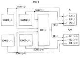
- FIG. 5 is a diagram illustrating stages of a shift register.
- FIG. 5 shows stages that are connected to pixels arranged along a j-th horizontal line and a (j+1)-th horizontal line (j is an odd number smaller than n)
- the j-th first scan signal stage SCAN1D[j] generates a j-th first scan signal SCAN1[j], and applies the j-th first scan signal SCAN1 to a j-th first scan line SL1[j].
- the (j+1)-th second scan signal stage SCAN2D[j+1] generates a (j+1)-th second scan signal SCAN2[j+1], and applies the (j+1)-th second scan signal SCAN2[j+1] to a (j+1)-th second scan line SL2[j+1].
- Pixels arranged along a pair of two adjacent horizontal lines are driven by the same emission control signal, so it is possible to drive pixels arranged along n number of horizontal lines with n/2 number of emission control signal stages. That is, it is possible to reduce the entire area of the shift register 140, and thus, reduce a bezel area of the non-display portion 100B.
- FIG. 6 is a circuit diagram illustrating an emission control signal stage.
- an emission control signal stage EMD1 that outputs a first emission control signal EM1 which is supplied to pixels arranged along a first horizontal line HL1 and a second horizontal line HL2.
- an emission control signal stage EMD1 of the first stage generates a first emission control signal EM1 by using a first first scan signal SCAN1[1], a first second scan signal SCAN2[1], a first emission clock ECLK1, a third emission clock ECLK3, a fifth emission clock ECLK5, a start signal EMVST, and a reset signal ERST.
- the first first scan signal SCAN1[1] and the first second scan signal SCAN2[1] respectively indicate the first scan signal SCAN1[1] and the second scan signal SCAN2[1], which are output by the first and second scan signal stages SCAN1D[1] and SCAN2D[1] of the first stage.
- the second first scan signal SCAN1[2] indicates a first scan signal SCAN1[2] output by the first scan signal stage SCAN1D[2] of the second stage.
- a third low-potential trigger transistor T11 includes a first electrode connected to an input terminal of the high-potential voltage GVDD, a second electrode connected to the QB node (QB), and a gate electrode connected to the output terminal of the first second scan signal SCAN2[1]. Accordingly, when the first second scan signal SCAN2[1] is applied, the third low-potential trigger transistor T11 charges the QB node (QB).
- a pull-up transistor T8 includes a first electrode connected to the high-potential voltage GVDD, a second electrode connected to an emission control signal output terminal EMO1, a gate electrode connected to the Q node (Q). Accordingly, when a Q node (Q) is charged, the pull-up transistor T8 is turned on and subsequently generates a first emission control signal EM1 at the level of the high-potential voltage GVDD to the emission control signal output terminal EMO1.
- FIG. 7 is a diagram illustrating timing of clocks and control signals input to the emission control signal stage. Referring to FIGS. 6 and 7 , there are provided descriptions about a process in which the first emission control signal stage EMD1 outputs the first emission control signal EM1.
- a first emission clock ECLK1 and a start signal EMVST are synchronized.
- the first transistor T1 is turned on by the first emission clock ECLK1
- the second transistor T2 is turned on by the start signal EMVST.
- the Q node (Q) and a boosting capacitor C are charged to the high-potential voltage GVDD bypassing the first and second transistors T1 and T2.
- the pull-up transistor T8 is turned on as a result of the Q node (Q) being charged, and the first emission control signal EM1 at the level of the high-potential voltage GVDD is output to the emission control signal output terminal EMO1.
- an emission control signal stage realized as one stage supplies an emission control signal to pixels arranged along a pair of horizontal lines, so it is possible to reduce the number of stages of the emission control signal stage that is configured to drive the entire display panel. As a result, a bezel area in which the emission control signal stage is disposed may be reduced.
Landscapes
- Engineering & Computer Science (AREA)
- Physics & Mathematics (AREA)
- Computer Hardware Design (AREA)
- General Physics & Mathematics (AREA)
- Theoretical Computer Science (AREA)
- Control Of Indicators Other Than Cathode Ray Tubes (AREA)
- Electroluminescent Light Sources (AREA)
- Control Of El Displays (AREA)
Abstract
Description
- The present disclosure relates to an Organic Light Emitting Diode (OLED) display.
- A Flat Panel Display (FPD) is widely used for a desktop monitor, a laptop, a Personal Distal Assistant (PDA), and any other mobile computer or mobile phone terminal, because the FPD is effective in achieving miniaturization and lightness. The FPD includes a Liquid Crystal Display (LCD), a Plasma Display Panel (PDP), a Field Emission Display (FED), and an Organic Light Emitting Diode (OLED) display.
- The OLED display has a fast response speed and a wide viewing angle, and is able to produce brightness with high luminous efficiency. Generally, an OLED display uses a scan transistor, which is turned on by a scan signal, to apply a data voltage to a gate electrode of a driving transistor, and enables an OLED to emit light using the data voltage supplied the driving transistor. In addition, the OLED display uses an emission control signal to perform switching of the driving transistor and a high-potential voltage input terminal.
- Driving circuits generating a scan signal and an emission control signal may be formed in a bezel area of a display panel by using a Gate In Pale (GIP) scheme. Recently, methods for reducing the bezel area have been studied to satisfy users' demands. However, it is difficult to reduce the size of the bezel area because of a GIP circuit.
- An Organic Light Emitting Diode (OLED) display according to the present disclosure includes a plurality of pixels, first and second scan signal stages, and emission control signal stages. Each of the pixels are arranged along n number of horizontal lines (n indicates a natural number), a first scan transistor connected to a gate electrode of a driving transistor, a second scan transistor connected to a source electrode of the driving transistor, and an emission control transistor connected to a drain electrode of the driving transistor. First scan signal stages output first scan signals sequentially to the first scan transistors of the horizontal lines. Second scan signal stages sequentially output second scan signals to the second scan transistors of the horizontal lines. Emission control signal stages output emission control signals having the same phase to emission control transistors of two adjacent horizontal lines.
- An Organic Light Emitting Diode (OLED) display according to various embodiments comprises: pixels respectively arranged along n horizontal lines (n indicates a natural number) and each pixel comprising a driving transistor, a first scan transistor connected to a gate electrode of the driving transistor, a second scan transistor connected to a source electrode of the driving transistor, and an emission control transistor connected to a drain electrode of the driving transistor; n first scan signal stages configured to output first scan signals sequentially to the first scan transistors of the horizontal lines; n second scan signal stages configured to output second scan signals sequentially to the second scan transistors of the horizontal lines; and (1/2)×n emission control signal stages configured to output emission control signals having the same phase to emission control transistors of two adjacent horizontal lines.
- In one or more embodiments, regarding each of the pixels, the source electrode of the driving transistor is connected to an OLED; the first scan transistor comprises a gate electrode for receiving the first scan signal, and first and second electrodes respectively connected to a data line and the gate electrode of the driving transistor; the second scan transistor comprises a gate electrode for receiving the second scan signal, and first and second electrode respectively connected to an initialization line and the source electrode of the driving transistor; and the emission control transistor comprises a gate electrode for receiving the emission control signal, and first and second electrodes respectively connected to a high-potential voltage source and the drain electrode of the driving transistor.
- In one or more embodiments, in an initialization period, the first scan transistor applies a reference voltage to the gate electrode of the driving transistor in response to the first scan signal, and the second transistor applies an initialization voltage to the source electrode of the driving transistor in response to the second scan signal.
- In one or more embodiments, in a sampling period, the second scan transistor is turned off to thereby render the source electrode of the driving transistor floating; the first scan transistor applies the reference voltage to the gate electrode of the driving transistor in response to the first scan signal; and the emission control transistor applies a current to the source electrode of the driving transistor in response to the emission control signal, so that a voltage of the source electrode of the driving transistor corresponds to a difference between the reference voltage and a threshold voltage of the driving transistor.
- In one or more embodiments, in a data writing period, the second scan transistor and the emission control transistor are turned off; and the first scan transistor charges a storage capacitor, which is connected between the gate electrode and the source electrode of the driving transistor, to a data voltage in response to the first scan signal.
- In one or more embodiments, a j-th emission control signal stage (j is a natural number smaller than n) outputting a j-th emission control signal comprises: a pull-up transistor configured to output a high-potential voltage to an emission control signal output terminal when a Q node is charged; a pull-down transistor configured to discharge a potential of the emission control signal output terminal to a low-potential voltage when a QB node is charged; a first low-potential trigger transistor configured to charge the QB node at the beginning of an initialization period; and a second low-potential trigger transistor configured to charge the QB node in a data writing period, and wherein the j-th emission control signal is applied to pixels arranged along a j-th horizontal line and a (j+1)-th horizontal line.
- In one or more embodiments, the first low-potential trigger transistor comprises a first electrode receiving a j-th first scan signal, a second electrode connected to the QB node, and a gate electrode connected to a clock signal input terminal which has a turn-on level voltage in the initialization period.
- In one or more embodiments, the second low-potential trigger transistor comprises a gate electrode receiving a (j+1)-th first scan signal, a first electrode connected to an emission reset input terminal which outputs a high level signal in the data writing period, and a second electrode connected to the QB node.
- In one or more embodiments, the (j+1)-th first scan signal is maintained at a voltage level that turns on the second low-potential trigger transistor in a data writing period for pixels arranged along the j-th horizontal line and in an initialization period for pixels arranged along the (j+1)-th horizontal line.
- In one or more embodiments, the OLED display further comprises a third low-potential trigger transistor having a first electrode connected to a high-potential voltage input terminal, a second electrode connected to the Q node, and a gate electrode connected to a (j+1)-th second scan signal.
- In one or more embodiments, the (j+1)-th second scan signal is maintained at a voltage level that turns on the third low-potential trigger transistor in a specific part of an initialization period and in a specific part of an emission period for the pixels arranged along the j-th horizontal line.
- In one or more embodiments, the first scan signal stage outputs a j-th first scan signal at a voltage level that turns on the first scan transistor in first and second initialization periods, a sampling period, and a data writing period for pixels arranged along a j-the horizontal line (j indicates a natural number smaller than n).
- In one or more embodiments, the second scan signal stage outputs a j-th second scan signal at a voltage level that turns on the second scan transistor in the second initialization period for the pixels arranged along the j-th horizontal line.
- In one or more embodiments, the emission control signal stage outputs a j-th emission control signal at a voltage level that turns on the emission control transistor in the sampling period for the pixels arranged along the j-th horizontal line.
- In one or more embodiments, the j-th emission control signal is at a voltage level that turns off the emission control transistor in the second initialization period and the data writing period for the pixels arranged along the (j+1)-th horizontal line.
- In one or more embodiments, the j-th emission control signal stage generates the j-th emission control signal by receiving j-th first and second scan signals and a (j+1)-th first scan signal.
- The accompanying drawings, which are included to provide a further understanding of the invention and are incorporated in and constitute a part of this specification, illustrate embodiments of the invention and together with the description serve to explain the principles of the invention. In the drawings:
-
FIG. 1 is a diagram illustrating an Organic Light Emitting Diode (OLED) display according to an embodiment of the present disclosure; -
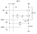
FIG. 2 is a diagram illustrating the structure of a pixel shown inFIG. 1 ; -
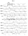
FIG. 3 is a diagram illustrating timing of control signals applied to the pixel shown inFIG. 2 ; -
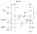
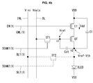
FIGS. 4A to 4D are diagrams illustrating a method of driving an OLED display according to an embodiment of the present disclosure; -
FIG. 5 is a diagram illustrating stages of a shift register according to an embodiment of the present disclosure; -
FIG. 6 is a circuit diagram illustrating an emission control signal stage; and -
FIG. 7 is a timing diagram illustrating input and output signals in the emission control signal stage shown inFIG. 6 . - Hereinafter, the embodiments disclosed in the present specification will be described in detail with reference to the accompanying drawings, and the same or similar elements are denoted by the same reference numerals even though they are depicted in different drawings and redundant descriptions thereof will be omitted.
-
FIG. 1 is an Organic Light Emitting Diode (OLED) display according to an embodiment of the present disclosure. - Referring to
FIG. 1 , the OLED display according an embodiment of the present disclosure includes adisplay panel 100 in which pixels P are arranged in matrix, adata driver 120, agate driver timing controller 110. - The
display panel 100 includes adisplay portion 100A in which the pixels P are arranged to display an image, and anon-display portion 100B in which ashift register 140 is arranged and which does not display an image. - A plurality of pixels P is included, and an image is displayed based on gray scales displayed by the pixels P. The pixels P are arranged along the first horizontal line HL1 to a n-the horizontal line HL[n].
- Each of the pixels P is connected to an initialization line INL and a data lines which are arranged along a column line, and connected to a first scan line SL1, a second scan line SL2, and an emission control signal line EML which are arranged along a horizontal line HL. In addition, each of the pixels P includes an OLED, a driving transistor DT, first and second scan transistors ST1 and ST2, an emission control transistor ET, a storage capacitor Cst, and a sub-capacitor Csub. Each of the transistors DT, ST1, ST2, and ET may be implemented as a Thin Film Transistor (TFT) including a polycrystalline semiconductor layer. However, aspects of the present disclosure are not limited thereto, and the semiconductor layer of the TFT may be formed of an amorphous silicon semiconductor or an oxide semiconductor.
- The
timing controller 110 is configured to control operation timing of thedata driver 120 and thegate driver timing controller 110 realigns externally received digital video data RGB to fit the resolution of thedisplay panel 100, and supplies the realigned digital video data RGB to thedata driver 120. In addition, thetiming controller 110 generates a control signal DDC for controlling operation timing of thedata driver 120, and a gate control signal GDC for controlling operation timing of thegate driver - The
data driver 120 is configured to drive data lines DL. To this end, thedata driver 120 converts digital video data RGB received from thetiming controller 110 into an analog data voltage based on the data control signal DDC, and supplies the analog data voltage to the data lines DL. In addition, thedata driver 120 supplies an initialization voltage Vini to the pixels P through an initialization line INL. - The
gate driver level shifter 130 and ashift register 140. Thelevel shifter 130 is formed as an Integrated Circuit (IC) on a Printed Circuit Board (PCB) (now shown) connected to thedisplay panel 100. Theshift register 140 is formed on thenon-display portion 100B of thedisplay panel 100 by using a Gate In Panel (GIP) scheme. - The
level shifter 130 performs level shifting of the clock signals CLK and a start signal VST under the control of the timing control, and supplies the level-shifted clock signals CLK and the level-shifted start signal VST. Theshift register 140 is formed as a combination of multiple TFTs in the non-display portion 100b of thedisplay panel 100 by using the GIP scheme. Theshift register 140 is comprised of stages which shift scan signals and output the shifted scan signal in response to the clock signals CLK and the start signal VST. The stages included in theshift register 140 output first scan signals SCAN1, second scan signals SCAN2, and emission control signal EM. -
FIG. 2 shows an example of a pixel P shown inFIG. 1 . - Referring to
FIG. 2 , the pixel P according to an embodiment of the present disclosure includes an OLED, a driving transistor DT, first and second scan transistors ST1 and ST2, an emission control transistor ET, a storage capacitor Cst, and a sub-capacitor Csub. - The OLED emits light by a driving current supplied from the driving transistor DT. Multiple organic compound layers are formed between an anode electrode and a cathode electrode of the OLED. The organic compound layers include Hole Injection layers (HIL), Hole transport layers (HTL), Emission layers (EML), Electron transport layers (ETL), and Electron Injection layers (EIL). The anode electrode of the OLED is connected to a source electrode of the driving transistor DT, and the cathode electrode of the OLED is connected to GVSS.
- The driving transistor DT uses its gate-source voltage to control a driving current which is to be applied to the OLED. To this end, the driving transistor DT includes a gate electrode connected to an input terminal of a data voltage Vdata, a drain voltage connected to an input terminal of a driving voltage VDD, and a source electrode connected to a low-potential driving voltage VSS.
- In response to a first scan signal, the first scan transistor ST1 applies a reference voltage Vref or a data voltage Vdata, which is received from the data line DL, to the gate electrode of the driving transistor DT. To this end, the first scan transistor ST1 includes a gate electrode connected to the first scan line SL1, a drain electrode connected to the data line DL, and a source electrode connected to a first node n1.
- In response to a second scan signal SCAN2, the second scan transistor ST2 provides an initialization voltage Vini, which is received from the initialization line INL, to a second node n2. To this end, the second scan transistor ST2 includes a gate electrode connected to the second scan line SL2, a drain electrode connected to the initialization line INL, and a source electrode connected to the second node n2.
- In response to an emission control signal, the emission control transistor ET controls a current path between the input terminal of the driving voltage VDD and the driving transistor DT. To this end, the emission control transistor ET includes a gate electrode connected to the emission control signal line EML, a drain electrode connected to the input terminal of the driving voltage VDD, and a source electrode connected to the driving transistor DT.
- The storage capacitor Cst maintains the data voltage Vdata, which is received from the data line DL, for one frame, so that the driving transistor DT can maintain a constant voltage. To this end, the storage capacitor Cst is connected to the gate electrode and the source electrode of the driving transistor DT.
- The sub-capacitor Csub is connected in series to the storage capacitor Cst at the second node n2 so as to adjust efficiency of the driving voltage Vdata.
- Operation of the pixel P in the above-described structure is described in the following.
FIG. 3 is a waveform diagram showing signals EM, SCAN, INIT, and DATA applied to the pixel P shown inFIG. 2 . - In the drawings, one horizontal period H indicates a scanning period of pixels arranged along one horizontal line HL. The scanning period includes a sampling period and a data writing period.
-
FIGS. 4A to 4D are equivalent circuits of a pixel P in an initialization period Ti, a sampling period Ts, a data writing period Tw, and an emission period Te. InFIGS. 4A to 4D , a solid line indicates each activated element or current path, and a dotted line indicates each inactivated element or current path.FIGS. 4A to 4D show operation of pixels P that are arranged, for example, along one horizontal line. - Operation of each pixel P according to an embodiment of the present disclosure includes: an initialization period Ti for initializing the first node n1 and the second node n2 to a specific voltage; a sampling period Ts for detecting a threshold voltage of the driving transistor DT; a data writing period Tw for writing a data voltage; and an emission period Te for emitting light by compensating for a driving current applied to an OLED, regardless of a threshold voltage.
- Referring to
FIGS. 3 and4A , the initialization period Ti includes a first initialization period Ti1 and a second initialization period Ti2. In the first and second initialization periods Ti1 and Ti2, the first scan signal SCAN1 is applied at the turn-on voltage level. In the second initialization period Ti2, the second scan signal SCAN2 is applied at the turn-on voltage level. In the first and second initialization period Ti1 and Ti2, the emission control signal EM is applied at the turn-off voltage level. - When the second scan signal SCAN2 is at a turn-on voltage level, the second scan transistor ST2 applies an initialization voltage Vini, which is received from the initialization line INL, to the second node n2. As a result, a source voltage Vs of the driving transistor DT acts as the initialization voltage Vini. When the first scan signal SCAN1 is at the turn-on voltage level, the first scan transistor ST1 applies a reference voltage Vref, which is received from the data line DL, to the first node n1. As a result, a gate voltage Vg of the driving transistor DT acts as the reference voltage Vref.
- The initialization voltage Vini is applied to the second node n2 in the initialization period T2 in an effort to initialize a concerned pixel to a specific level. In this case, the initialization voltage Vini is set to be smaller than an operation voltage of the OLED to prevent the OLED from emitting light.
- Referring to
FIGS. 3 and4B , in the sampling period Ts, the second scan signal SCAN2 is reversed to the turn-off voltage level, the emission control signal EM is reversed to the turn-on voltage level, and the first scan signal SCAN1 remains at the turn-on voltage level. - In response to the first scan signal SCAN1, the first scan transistor ST1 applies the reference voltage Vref, which is received from the data line DL, to the first node n1. In response to the emission control signal EM, the emission control transistor ET applies a driving voltage VDD to the driving transistor DT.
- When the second node n2 is floating as a result of the second scan transistor ST2 being turned off, a voltage of the second node n2 gradually increases due to a current flowing from the drain electrode of the driving transistor DT to the source electrode thereof. In this case, the first node n1 remains at the reference voltage Vref, so the second node n2 is saturated with a voltage which corresponds to difference between the reference voltage Vref and the threshold voltage Vth of the driving transistor DT. That is, in the sampling period Ts, a gate-source potential difference of the driving transistor DT becomes to have the size equal to that of the threshold voltage Vth.
- Referring to
FIGS. 3 and4C , in the data writing period Tw, the first scan signal SCAN1 remains at the turn-on voltage level, the second scan signal SCAN2 remains at the turn-off voltage level, and the emission control signal EM is reversed to the turn-off voltage level. - In response to the first scan signal SCAN1, the first scan transistor ST1 supplies a data voltage Vdata, which is received from the data line DL, to the first node n1. At this point, a voltage of the second node n2 in a floating state rises or falls because coupling effects occur due to the ratio of capacitance between the storage capacitor Cst to a sub-capacitor C1.
- Referring to
FIGS. 3 and4D , in the emission period Te, the first scan signal SCAN1 is reversed to the turn-off voltage level, the second scan signal SCAN2 remains at the turn-off voltage level, and the emission control signal EM is reversed to the turn-on voltage level. - In the emission period Te, the data voltage Vdata stored in the storage capacitor Cst is supplied to the OLED, so the OLED emits light with brightness which is in proportion to the data voltage Vdata. At this point, a current flows in the driving transistor DT by the voltages of the first and second nodes n1 and n2 determined in the data writing period Tw, so a desired current is supplied to the OLED. As a result, the OLED is able to control brightness using the data voltage Vdata.
-
FIG. 5 is a diagram illustrating stages of a shift register.FIG. 5 shows stages that are connected to pixels arranged along a j-th horizontal line and a (j+1)-th horizontal line (j is an odd number smaller than n) - Referring to
FIG. 5 , stages for driving pixels arranged along a pair of two adjacent horizontal lines HLj and HL[j+1] include a j-th first scan signal stage SCAN1D[j], a j-th second scan signal stage SCAN2D[j], a (j+1)-th first scan signal stage SCAN1D[j+1], a (j+1)-th second scan signal stage SCAN2D[j+1], and a j-th emission control signal stage EMD[j]. - The j-th first scan signal stage SCAN1D[j] generates a j-th first scan signal SCAN1[j], and applies the j-th first scan signal SCAN1 to a j-th first scan line SL1[j].
- The j-th second scan signal stage SCAN2D[j] generates a j-th second scan signal SCAN2[j], and applies the j-th second scan signal SCAN2[j] to a j-th second scan line SL2[j].
- The (j+1)-th first scan signal stage SCAN1D[j+1] generates a (j+1)-th first scan signal SCAN1[j+1], and applies the (j+1)-th first scan signal SCAN1[j+1] to a (j+1)-th first scan line SL1[j+1].
- The (j+1)-th second scan signal stage SCAN2D[j+1] generates a (j+1)-th second scan signal SCAN2[j+1], and applies the (j+1)-th second scan signal SCAN2[j+1] to a (j+1)-th second scan line SL2[j+1].
- The j-th emission control signal stage EMD[j] generates a j-th emission control signal EM[j], and applies the j-th emission control signal EM[j] to a j-th emission control signal line EML[j] connected to pixels Pj arranged along the j-th horizontal line and a (j+1)-th emission control signal line EML[j+1] connected to pixels P[j+1] arranged along the (j+1)-th horizontal line. The j-th emission control signal stage EMD[j] is used as a clock signal for controlling operation timing of each transistor by receiving a j-th first scan signal SCAN1, a j-th second scan signal SCAN2, and a (j+1)-th first scan signal SCAN1.
- Pixels arranged along a pair of two adjacent horizontal lines are driven by the same emission control signal, so it is possible to drive pixels arranged along n number of horizontal lines with n/2 number of emission control signal stages. That is, it is possible to reduce the entire area of the
shift register 140, and thus, reduce a bezel area of thenon-display portion 100B. -
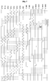
FIG. 6 is a circuit diagram illustrating an emission control signal stage. In particular, it shows an emission control signal stage EMD1 that outputs a first emission control signal EM1 which is supplied to pixels arranged along a first horizontal line HL1 and a second horizontal line HL2. - Referring to
FIGS. 6 and7 , an emission control signal stage EMD1 of the first stage generates a first emission control signal EM1 by using a first first scan signal SCAN1[1], a first second scan signal SCAN2[1], a first emission clock ECLK1, a third emission clock ECLK3, a fifth emission clock ECLK5, a start signal EMVST, and a reset signal ERST. The first first scan signal SCAN1[1] and the first second scan signal SCAN2[1] respectively indicate the first scan signal SCAN1[1] and the second scan signal SCAN2[1], which are output by the first and second scan signal stages SCAN1D[1] and SCAN2D[1] of the first stage. The second first scan signal SCAN1[2] indicates a first scan signal SCAN1[2] output by the first scan signal stage SCAN1D[2] of the second stage. - Similarly, instead of the first emission clock ECLK1, the third emission clock ECLK3, and the fifth emission clock ECLK5, the j-th emission control signal stage EMD[j] receives a j-th emission clock ECLKj, a (j+2)-th emission clock ECLK[j+2], and a (j+4)-th emission clock ECLK[j+4].
- The emission clock ECLK consists of seven phases, and each clock signal is continuous. Thus, for a clock signal having (j+k) which is greater than 7 (k indicates a natural number satisfying the condition of 1<k<7), a cock signal with an ordinal number cut by 7 is used. For example, a (j+4)-th gate clock GCLK[j+4] in the fifth emission control signal stage corresponds to a second gate clock GCLK2.
- The first transistor T1A includes a first electrode connected to an input terminal of the high-potential voltage GVDD, a second electrode connected to a first electrode of a second transistor T2, and a gate electrode connected to an input terminal of the first emission clock ECLK1. The second transistor T2 includes the first electrode connected to the second electrode of the first transistor T1, a second electrode connected to a Q node (Q), and a gate electrode connected to an input terminal of the start signal EMVST. When the emission clock ECLK1 and the start signal EMVST are synchronized, the first and second transistors T1 and T2 are all turned on, and accordingly, the Q node (Q) is charged to the high-potential voltage GVDD provided through the first and second transistors T1 and T2.
- A first low-potential trigger transistor T6 include a first electrode connected to an output terminal of the first first scan signal SCAN1[1], a second electrode connected to a QB node (QB), and a gate electrode connected to the input terminal of the fifth emission clock ECLK5. Accordingly, when the fifth emission clock ECLK5 and the first first scan signal SCAN1[1] are synchronized, the first low-potential trigger transistor T5 charges the QB node (QB).
- A second low-potential trigger transistor T3 includes a first electrode connected to an input terminal of the emission reset signal ERST, a second electrode connected to the QB node (QB), and a gate electrode connected to an output terminal of the second first scan signal SCAN1[2]. Accordingly, when the emission reset signal ERST and the second first scan signal SCAN1[2] are synchronized, the second low-potential trigger transistor T3 charges the QB node (QB).
- A third low-potential trigger transistor T11 includes a first electrode connected to an input terminal of the high-potential voltage GVDD, a second electrode connected to the QB node (QB), and a gate electrode connected to the output terminal of the first second scan signal SCAN2[1]. Accordingly, when the first second scan signal SCAN2[1] is applied, the third low-potential trigger transistor T11 charges the QB node (QB).
- A fourth transistor T4 includes a first electrode connected to a high-potential voltage GVDD, a second electrode connected to a second electrode of a ninth transistor T9 and a gate electrode connected to an emission control signal output terminal EMO1.
- The sixth transistor T6 includes a first electrode connected to the Q node (Q), a second electrode connected to an input terminal of the low-potential voltage GVSS, and a gate electrode connected to the QB node (QB). Accordingly, when the QB node (QB) is charged, the sixth transistor T6 discharges the Q node (Q) to the low-potential voltage GVSS.
- A seventh transistor T7 includes a first electrode connected to the QB node (QB), a second electrode connected to the low-potential voltage GVSS, a gate electrode connected to an input terminal of the third emission clock ECLK3. Accordingly, the seventh transistor T7 discharges the QB node (QB) in response to the third emission clock ECLK3.
- A pull-up transistor T8 includes a first electrode connected to the high-potential voltage GVDD, a second electrode connected to an emission control signal output terminal EMO1, a gate electrode connected to the Q node (Q). Accordingly, when a Q node (Q) is charged, the pull-up transistor T8 is turned on and subsequently generates a first emission control signal EM1 at the level of the high-potential voltage GVDD to the emission control signal output terminal EMO1.
- Pull-down transistors T9 and T10 are connected in series to each other. Each of the pull-down transistors T9 and T10 includes a gate electrode connected to the QB node (QB). A first electrode of the ninth transistor T9 is connected to the emission control signal output terminal EMO1, and a second electrode of the tenth transistor T10 is connected to the low-potential voltage GVSS. Accordingly, the pull-down transistors T9 and T10 discharges the potential of the emission control signal output terminal EMO1 to the low-potential voltage GVSS in response to the potential of the QB node (QB).
-
FIG. 7 is a diagram illustrating timing of clocks and control signals input to the emission control signal stage. Referring toFIGS. 6 and7 , there are provided descriptions about a process in which the first emission control signal stage EMD1 outputs the first emission control signal EM1. - During a first initialization period Ti1, the first first scan signal SCAN1[1] and a fifth emission clock ECLK5 are synchronized. As a result, the first low-potential trigger transistor T5 is turned on, thereby charging the QB node (QB) to a voltage of the fifth emission clock ECLK5. The pull-down transistors T9 and T10 are turned on as a result of the QB node (QB) being charged, and the emission control signal output terminal EMO1 is discharged to the low-potential voltage GVSS. As a result, an emission control signal, which was output at a high-level voltage in an emission period of a previous frame, is reversed to low level at the beginning of the first initialization period Ti1.
- In the sampling period Ts, a first emission clock ECLK1 and a start signal EMVST are synchronized. The first transistor T1 is turned on by the first emission clock ECLK1, and the second transistor T2 is turned on by the start signal EMVST. As the first and second transistors T1 and T2 are turned on at the same time, the Q node (Q) and a boosting capacitor C are charged to the high-potential voltage GVDD bypassing the first and second transistors T1 and T2. The pull-up transistor T8 is turned on as a result of the Q node (Q) being charged, and the first emission control signal EM1 at the level of the high-potential voltage GVDD is output to the emission control signal output terminal EMO1.
- In the data writing period Tw, the first scan signal SCAN1 of the second stage and a reset signal ERST are synchronized. As a result, the second low-potential trigger transistor T3 is turned on, thereby charging the QB node (QB) using the reset signal ERST. The pull-down transistors T9 and T10 are turned on as a result of the QB node (QB) being charged, and the emission control signal output terminal EMO1 is discharged to the low-potential voltage GVSS.
- At the beginning of the emission period Te, a first emission clock ECLK1 and the start signal EMVST are synchronized. The first transistor T1 is turned on by the first emission clock ECLK1, and the second transistor T2 is turned on by the start signal EMVST. As the first and second transistors T1 and T2 are turned on at the same time, the Q node (Q) and the boosting capacitor C are charged to the high-potential voltage GVDD bypassing the first and second transistors T1 and T2. The pull-up transistor T8 is turned on as a result of the Q node (Q) being charged, and the first emission control signal EM1 at the level of the high-potential voltage GVDD is output to the emission control signal output terminal EMO1.
- In the emission period Te, the seventh transistor T7 is turned on at a specific interval in response to a third emission clock ECLK3. In a turn-on state, the seventh transistor T7 maintains the QB node (QB) at low-potential voltage in order to restrain the pull-down transistors T9 and T10 from turning on. That is, the seventh transistor T7 enables the first emission control signal EM1 to be stably output through the emission control signal output terminal EMO1 in the emission period Te.
- In the emission period Te, the tenth transistor T10 is turned on by the first second scan signal SCAN2[1]. When the tenth transistor T10 is turned on, the QB node (QB) is charged, thereby rendering the pull-down transistors T9 and T10 turned on. The pull-down transistors T9 and T10 are turned on, thereby discharging the voltage of the emission control signal output terminal EMO1. That is, the first second scan signal SCAN2[1] applied in the emission period Te stops outputting of the first emission control signal EM1. The voltage of the emission control signal output terminal EMO1, which is discharged by the first second scan signal SCAN2[1], is maintained to be a low-potential voltage until the first emission clock ECLK1 and the start signal EMVST are synchronized.
- As such, the emission period Te is divided into a period of outputting the emission control signal EM and a period of suppressing the emission control signal EM, so it is possible to drive pixels at duty cycles.
- The first emission control signal EM1 according to the present disclosure is applied at the same time not just to pixels arranged along the first horizontal line HL1, but to pixels arranged along the second horizontal line HL2. Thus, the first emission control signal EM1 has to satisfy driving requirements not just of the pixels arranged along the first horizontal line HL1, but of the pixels arranged along the second horizontal line HL2. The data writing period Tw2 of the pixels arranged along the second horizontal line corresponds to a specific part of the emission period TE of the pixels arranged along the first horizontal line HL1. In the data writing period Tw of the pixels arranged along the second horizontal line HL2, the second first scan signal SCAN 1 [2] and the reset signal ERST turn off the second low-potential trigger transistor T3. That is, the first emission control signal EM1 may drive not just the pixels arranged along the first horizontal line HL1, but the pixels arranged along the second horizontal line HL2 at the same time.
- In the OLED display according to the present disclosure, an emission control signal stage realized as one stage supplies an emission control signal to pixels arranged along a pair of horizontal lines, so it is possible to reduce the number of stages of the emission control signal stage that is configured to drive the entire display panel. As a result, a bezel area in which the emission control signal stage is disposed may be reduced.
- Although embodiments have been described with reference to a number of illustrative embodiments thereof, it should be understood that numerous other modifications and embodiments can be devised by those skilled in the art that will fall within the scope of the principles of this disclosure. More particularly, various variations and modifications are possible in the component parts and/or arrangements of the subject combination arrangement within the scope of the disclosure, the drawings and the appended claims. In addition to variations and modifications in the component parts and/or arrangements, alternative uses will also be apparent to those skilled in the art.
Claims (16)
- An Organic Light Emitting Diode display comprising:pixels (P) respectively arranged along n horizontal lines (HL1, ..., HLn), wherein n indicates a natural number, and each pixel (P) comprising a driving transistor (DT), a first scan transistor (ST1) connected to a gate electrode of the driving transistor (DT), a second scan transistor (ST2) connected to a source electrode of the driving transistor (DT), and an emission control transistor (ET) connected to a drain electrode of the driving transistor (DT);n first scan signal stages configured to output first scan signals (SCAN1) sequentially to the first scan transistors (ST1) of the horizontal lines (HL1, ..., HLn);n second scan signal stages configured to output second scan signals (SCAN2) sequentially to the second scan transistors (ST2) of the horizontal lines (HL1, ..., HLn); and (1/2)×n emission control signal stages configured to output emission control signals (EM) having the same phase to emission control transistors (ET) of two adjacent horizontal lines.
- The Organic Light Emitting Diode display of claim 1, wherein:regarding each of the pixels (P),the source electrode of the driving transistor (DT) is connected to an Organic Light Emitting Diode (OLED);the first scan transistor (ST1) comprises a gate electrode for receiving the first scan signal (SCAN1), and first and second electrodes respectively connected to a data line (DL) and the gate electrode of the driving transistor (DT);the second scan transistor (ST2) comprises a gate electrode for receiving the second scan signal (SCAN2), and first and second electrodes respectively connected to an initialization line (INL) and the source electrode of the driving transistor (DT); andthe emission control transistor (ET) comprises a gate electrode for receiving the emission control signal (EM), and first and second electrodes respectively connected to a high-potential voltage source and the drain electrode of the driving transistor (DT).
- The Organic Light Emitting Diode display of claim 2, wherein:in an initialization period (Ti),the first scan transistor (ST1) applies a reference voltage (Vref) to the gate electrode of the driving transistor (DT) in response to the first scan signal (SCAN1), andthe second scan transistor (ST2) applies an initialization voltage (Vini) to the source electrode of the driving transistor (DT) in response to the second scan signal (SCAN2).
- The Organic Light Emitting Diode display of claim 3, wherein:in a sampling period (Ts),the second scan transistor (ST2) is turned off to thereby render the source electrode of the driving transistor (DT) floating;the first scan transistor (ST1) applies the reference voltage (Vref) to the gate electrode of the driving transistor (DT) in response to the first scan signal (SCAN1); andthe emission control transistor (ET) applies a current to the source electrode of the driving transistor (DT) in response to the emission control signal (EM), so that a voltage of the source electrode of the driving transistor (DT) corresponds to a difference between the reference voltage (Vref) and a threshold voltage of the driving transistor (DT).
- The Organic Light Emitting Diode display of claim 1 or 4, wherein:in a data writing period (Tw),the second scan transistor (ST2) and the emission control transistor (ET) are turned off; andthe first scan transistor (ST1) charges a storage capacitor (Cst), which is connected between the gate electrode and the source electrode of the driving transistor (DT), to a data voltage (Vdata) in response to the first scan signal (SCAN1).
- The Organic Light Emitting Diode display of any one of claims 1 to 5, wherein a j-th emission control signal stage (EMD(j)), wherein(j is a natural number smaller than n, outputting a j-th emission control signal (EM(j)) comprises:a pull-up transistor (T8) configured to output a high-potential voltage (GVDD) to an emission control signal output terminal (EMO) when a Q node is charged;a pull-down transistor (T9, T10) configured to discharge a potential of the emission control signal output terminal (EMO) to a low-potential voltage (GVSS) when a QB node is charged;a first low-potential trigger transistor (T5) configured to charge the QB node at the beginning of an initialization period (Ti); anda second low-potential trigger transistor (T3) configured to charge the QB node in a data writing period (Tw), andwherein the j-th emission control signal (EM(j)) is applied to pixels (Pj, Pj+1) arranged along a j-th horizontal line and a (j+1)-th horizontal line.
- The Organic Light Emitting Diode display of claim 6, wherein the first low-potential trigger transistor (T5) comprises a first electrode receiving a j-th first scan signal (SCAN1(j)), a second electrode connected to the QB node, and a gate electrode connected to a clock signal input terminal which has a turn-on level voltage in the initialization period (Ti).
- The Organic Light Emitting Diode display of claim 6 or 7, wherein the second low-potential trigger transistor (T3) comprises a gate electrode receiving a (j+1)-th first scan signal (SCAN1(j)), a first electrode connected to an emission reset input terminal which outputs a high level signal in the data writing period (Tw), and a second electrode connected to the QB node.
- The Organic Light Emitting Diode display of claim 8, wherein the (j+1)-th first scan signal (SCAN1(j)) is maintained at a voltage level that turns on the second low-potential trigger transistor (T3) in a data writing period (Tw) for pixels (Pj) arranged along the j-th horizontal line and in an initialization period (Ti) for pixels (Pj+1) arranged along the (j+1)-th horizontal line.
- The Organic Light Emitting Diode display of any one of claims 6 to 9, further comprising a third low-potential trigger transistor (T11) having a first electrode connected to a high-potential voltage input terminal, a second electrode connected to the Q node, and a gate electrode connected to a (j+1)-th second scan signal (SCAN2(j+1)).
- The Organic Light Emitting Diode display of claim 10, wherein the (j+1)-th second scan signal (SCAN2(j+1)) is maintained at a voltage level that turns on the third low-potential trigger transistor (T11) in a specific part of an initialization period (Ti) and in a specific part of an emission period (Te) for the pixels (Pj) arranged along the j-th horizontal line.
- The Organic Light Emitting Diode display of claim 1, wherein the first scan signal stage outputs a j-th first scan signal (SCAN1(j)) at a voltage level that turns on the first scan transistor (ST1) in first and second initialization periods (Ti1, Ti2), a sampling period (Ts), and a data writing period (Tw) for pixels (Pj) arranged along a j-the horizontal line, wherein j indicates a natural number smaller than n.
- The Organic Light Emitting Diode display of claim 12, wherein the second scan signal stage outputs a j-th second scan signal (SCAN2(j)) at a voltage level that turns on the second scan transistor (ST2) in the second initialization period (Ti2) for the pixels (Pj) arranged along the j-th horizontal line.
- The Organic Light Emitting Diode display of claim 13, wherein the emission control signal stage outputs a j-th emission control signal (EM(j)) at a voltage level that turns on the emission control transistor (ET) in the sampling period (Ts) for the pixels (Pj) arranged along the j-th horizontal line.
- The Organic Light Emitting Diode display of claim 14, wherein the j-th emission control signal (EM(j)) is at a voltage level that turns off the emission control transistor (ET) in the second initialization period (Ti2) and the data writing period (Tw) for the pixels (Pj) arranged along the (j+1)-th horizontal line.
- The Organic Light Emitting Diode display of claim 14 or 15, wherein the j-th emission control signal stage generates the j-th emission control signal (EM(j)) by receiving j-th first and second scan signals (SCAN1(j), SCAN2(j)) and a (j+1)-th first scan signal (SCAN1(j+1)).
Applications Claiming Priority (1)
| Application Number | Priority Date | Filing Date | Title |
|---|---|---|---|
| KR1020150138251A KR102503160B1 (en) | 2015-09-30 | 2015-09-30 | Organic Light Emitting diode Display |
Publications (2)
| Publication Number | Publication Date |
|---|---|
| EP3151233A1 true EP3151233A1 (en) | 2017-04-05 |
| EP3151233B1 EP3151233B1 (en) | 2021-08-11 |
Family
ID=57083131
Family Applications (1)
| Application Number | Title | Priority Date | Filing Date |
|---|---|---|---|
| EP16191065.8A Active EP3151233B1 (en) | 2015-09-30 | 2016-09-28 | Organic light emitting diode display |
Country Status (4)
| Country | Link |
|---|---|
| US (1) | US10223969B2 (en) |
| EP (1) | EP3151233B1 (en) |
| KR (1) | KR102503160B1 (en) |
| CN (1) | CN107146575B (en) |
Families Citing this family (32)
| Publication number | Priority date | Publication date | Assignee | Title |
|---|---|---|---|---|
| KR102382323B1 (en) * | 2015-09-30 | 2022-04-05 | 엘지디스플레이 주식회사 | Organic Light Emitting Diode Display |
| KR102446050B1 (en) * | 2016-01-19 | 2022-09-23 | 삼성디스플레이 주식회사 | Scan driving circuit and organic light emitting diode display including same |
| KR102721846B1 (en) * | 2016-11-30 | 2024-10-24 | 엘지디스플레이 주식회사 | Emission driver for display device and disaplay device applying thereof |
| KR102573334B1 (en) * | 2016-12-28 | 2023-09-01 | 엘지디스플레이 주식회사 | Light emitting display device and driving method for the same |
| KR102332423B1 (en) * | 2017-07-27 | 2021-11-30 | 엘지디스플레이 주식회사 | Shift Resistor and Display Device having the Same |
| KR102411045B1 (en) * | 2017-08-16 | 2022-06-17 | 엘지디스플레이 주식회사 | Display panel using gate driving circuit |
| KR102401937B1 (en) * | 2017-08-16 | 2022-05-24 | 엘지디스플레이 주식회사 | Gate driving circuit and display device using the same |
| KR102436560B1 (en) * | 2017-08-31 | 2022-08-26 | 엘지디스플레이 주식회사 | Gate driving circuit and organic light emitting display using the same |
| KR102498500B1 (en) * | 2017-09-15 | 2023-02-10 | 엘지디스플레이 주식회사 | Organic Light Display Device |
| JP7116539B2 (en) * | 2017-11-27 | 2022-08-10 | 株式会社ジャパンディスプレイ | Display device |
| KR102470378B1 (en) * | 2017-11-30 | 2022-11-23 | 엘지디스플레이 주식회사 | Gate driving circuit and light emitting display apparatus comprising the same |
| EP3493189B1 (en) * | 2017-11-30 | 2023-08-30 | LG Display Co., Ltd. | Electroluminescent display device |
| KR102595130B1 (en) * | 2017-12-07 | 2023-10-26 | 엘지디스플레이 주식회사 | Light emitting display apparatus and method for driving thereof |
| KR102711314B1 (en) | 2018-06-28 | 2024-09-27 | 삼성디스플레이 주식회사 | Organic light emitting diode display device |
| KR102649177B1 (en) * | 2018-10-11 | 2024-03-19 | 엘지디스플레이 주식회사 | Gate drivign circuit, display panel and display device |
| KR102680571B1 (en) * | 2018-12-04 | 2024-07-04 | 엘지디스플레이 주식회사 | Organic light emitting display apparatus |
| KR102598383B1 (en) * | 2018-12-10 | 2023-11-06 | 엘지디스플레이 주식회사 | Display device and signal inversion device |
| KR102840041B1 (en) | 2019-12-16 | 2025-07-28 | 엘지디스플레이 주식회사 | Gate driver and display device including the same |
| KR102802516B1 (en) * | 2019-12-17 | 2025-05-02 | 엘지디스플레이 주식회사 | Display device |
| KR102727655B1 (en) | 2019-12-23 | 2024-11-06 | 엘지디스플레이 주식회사 | Gate driver and display device including the same |
| JP6923015B2 (en) * | 2020-01-17 | 2021-08-18 | セイコーエプソン株式会社 | Display devices and electronic devices |
| KR20220000001A (en) * | 2020-06-23 | 2022-01-03 | 삼성디스플레이 주식회사 | Display device |
| CN112164364B (en) * | 2020-10-26 | 2022-07-26 | 合肥维信诺科技有限公司 | Driving circuit of display panel, display panel and driving method thereof |
| KR102755207B1 (en) * | 2020-12-17 | 2025-01-20 | 엘지디스플레이 주식회사 | Display device and gate driving circuit |
| KR102851042B1 (en) * | 2021-11-18 | 2025-08-27 | 엘지디스플레이 주식회사 | Electroluminescent display device |
| KR102862796B1 (en) * | 2021-12-16 | 2025-09-22 | 엘지디스플레이 주식회사 | Electroluminescence Display Device |
| CN114203109B (en) * | 2021-12-20 | 2022-12-13 | 长沙惠科光电有限公司 | Pixel driving circuit, compensation method thereof and display panel |
| US11915656B2 (en) * | 2021-12-29 | 2024-02-27 | Lg Display Co., Ltd. | Gate driver and display device including the same |
| KR102878302B1 (en) * | 2021-12-30 | 2025-10-28 | 엘지디스플레이 주식회사 | Viewing Angle Switchable Emission Signal Generating Part And Viewing Angle Switchable Display Device Including The Same |
| CN117765883A (en) * | 2022-09-19 | 2024-03-26 | 京东方科技集团股份有限公司 | Pixel driving circuit and driving method thereof, display panel, display device |
| KR20240076034A (en) | 2022-11-23 | 2024-05-30 | 엘지디스플레이 주식회사 | Pixel circuit and display device including the same |
| WO2024259590A1 (en) * | 2023-06-20 | 2024-12-26 | Boe Technology Group Co., Ltd. | Display apparatus |
Citations (3)
| Publication number | Priority date | Publication date | Assignee | Title |
|---|---|---|---|---|
| CN103150992A (en) * | 2013-03-14 | 2013-06-12 | 友达光电股份有限公司 | Pixel driving circuit |
| US20130314308A1 (en) * | 2012-05-22 | 2013-11-28 | Au Optronics Corporation | Organic light emitting display unit structure and organic light emitting display unit circuit |
| US20140111557A1 (en) * | 2012-10-19 | 2014-04-24 | Japan Display Inc. | Display apparatus |
Family Cites Families (5)
| Publication number | Priority date | Publication date | Assignee | Title |
|---|---|---|---|---|
| TW594634B (en) * | 2003-02-21 | 2004-06-21 | Toppoly Optoelectronics Corp | Data driver |
| TWI224300B (en) * | 2003-03-07 | 2004-11-21 | Au Optronics Corp | Data driver and related method used in a display device for saving space |
| KR101184065B1 (en) * | 2005-06-25 | 2012-09-18 | 엘지디스플레이 주식회사 | Organic Light Emitting Diode Display |
| KR102089325B1 (en) * | 2013-09-30 | 2020-03-16 | 엘지디스플레이 주식회사 | Organic light emitting diode display device and method for driving the same |
| KR102076845B1 (en) * | 2013-11-08 | 2020-02-12 | 엘지디스플레이 주식회사 | The Method for Driving of Organic Light Emitting diode Display |
-
2015
- 2015-09-30 KR KR1020150138251A patent/KR102503160B1/en active Active
-
2016
- 2016-09-27 US US15/277,827 patent/US10223969B2/en active Active
- 2016-09-28 EP EP16191065.8A patent/EP3151233B1/en active Active
- 2016-09-28 CN CN201610862181.8A patent/CN107146575B/en active Active
Patent Citations (3)
| Publication number | Priority date | Publication date | Assignee | Title |
|---|---|---|---|---|
| US20130314308A1 (en) * | 2012-05-22 | 2013-11-28 | Au Optronics Corporation | Organic light emitting display unit structure and organic light emitting display unit circuit |
| US20140111557A1 (en) * | 2012-10-19 | 2014-04-24 | Japan Display Inc. | Display apparatus |
| CN103150992A (en) * | 2013-03-14 | 2013-06-12 | 友达光电股份有限公司 | Pixel driving circuit |
Also Published As
| Publication number | Publication date |
|---|---|
| US20170092199A1 (en) | 2017-03-30 |
| US10223969B2 (en) | 2019-03-05 |
| CN107146575A (en) | 2017-09-08 |
| KR20170039051A (en) | 2017-04-10 |
| CN107146575B (en) | 2019-07-16 |
| KR102503160B1 (en) | 2023-02-24 |
| EP3151233B1 (en) | 2021-08-11 |
Similar Documents
| Publication | Publication Date | Title |
|---|---|---|
| EP3151233B1 (en) | Organic light emitting diode display | |
| US9646535B2 (en) | Organic light emitting display device | |
| US9715852B2 (en) | Organic light emitting display device | |
| US10891903B2 (en) | Gate-in-panel gate driver and organic light emitting display device having the same | |
| US10255860B2 (en) | Organic light emitting diode display | |
| US10373563B2 (en) | Organic light emitting diode (OLED) display | |
| US9454935B2 (en) | Organic light emitting diode display device | |
| US20150356913A1 (en) | Gate driving circuit and organic light emitting display device having the same | |
| KR20160073928A (en) | Organic Light Emitting Diode Display Device and Driving Method thereof | |
| CN113129838B (en) | Gate drive circuit and display device using the same | |
| US11205389B2 (en) | Scan driver and display device having same | |
| KR20190021985A (en) | Organic Light Emitting Display | |
| KR20190032959A (en) | Shift Resiter and Organic Light Emitting Display having the Same | |
| KR102364098B1 (en) | Organic Light Emitting Diode Display Device | |
| KR102332423B1 (en) | Shift Resistor and Display Device having the Same | |
| KR102202798B1 (en) | Organic Light Emitting Diode | |
| KR102436560B1 (en) | Gate driving circuit and organic light emitting display using the same | |
| US10255845B2 (en) | Gate driver and a display apparatus including the same | |
| KR102550292B1 (en) | Display Panel and Organic Light Emitting Display having the Same | |
| KR102299155B1 (en) | Organic Light Emitting Diode |
Legal Events
| Date | Code | Title | Description |
|---|---|---|---|
| PUAI | Public reference made under article 153(3) epc to a published international application that has entered the european phase |
Free format text: ORIGINAL CODE: 0009012 |
|
| STAA | Information on the status of an ep patent application or granted ep patent |
Free format text: STATUS: REQUEST FOR EXAMINATION WAS MADE |
|
| 17P | Request for examination filed |
Effective date: 20160928 |
|
| AK | Designated contracting states |
Kind code of ref document: A1 Designated state(s): AL AT BE BG CH CY CZ DE DK EE ES FI FR GB GR HR HU IE IS IT LI LT LU LV MC MK MT NL NO PL PT RO RS SE SI SK SM TR |
|
| AX | Request for extension of the european patent |
Extension state: BA ME |
|
| RBV | Designated contracting states (corrected) |
Designated state(s): AL AT BE BG CH CY CZ DE DK EE ES FI FR GB GR HR HU IE IS IT LI LT LU LV MC MK MT NL NO PL PT RO RS SE SI SK SM TR |
|
| STAA | Information on the status of an ep patent application or granted ep patent |
Free format text: STATUS: EXAMINATION IS IN PROGRESS |
|
| R17P | Request for examination filed (corrected) |
Effective date: 20160928 |
|
| 17Q | First examination report despatched |
Effective date: 20191112 |
|
| GRAP | Despatch of communication of intention to grant a patent |
Free format text: ORIGINAL CODE: EPIDOSNIGR1 |
|
| STAA | Information on the status of an ep patent application or granted ep patent |
Free format text: STATUS: GRANT OF PATENT IS INTENDED |
|
| INTG | Intention to grant announced |
Effective date: 20210309 |
|
| GRAS | Grant fee paid |
Free format text: ORIGINAL CODE: EPIDOSNIGR3 |
|
| GRAA | (expected) grant |
Free format text: ORIGINAL CODE: 0009210 |
|
| STAA | Information on the status of an ep patent application or granted ep patent |
Free format text: STATUS: THE PATENT HAS BEEN GRANTED |
|
| AK | Designated contracting states |
Kind code of ref document: B1 Designated state(s): AL AT BE BG CH CY CZ DE DK EE ES FI FR GB GR HR HU IE IS IT LI LT LU LV MC MK MT NL NO PL PT RO RS SE SI SK SM TR |
|
| REG | Reference to a national code |
Ref country code: CH Ref legal event code: EP |
|
| REG | Reference to a national code |
Ref country code: DE Ref legal event code: R096 Ref document number: 602016061907 Country of ref document: DE |
|
| REG | Reference to a national code |
Ref country code: IE Ref legal event code: FG4D Ref country code: AT Ref legal event code: REF Ref document number: 1420197 Country of ref document: AT Kind code of ref document: T Effective date: 20210915 |
|
| REG | Reference to a national code |
Ref country code: LT Ref legal event code: MG9D |
|
| REG | Reference to a national code |
Ref country code: NL Ref legal event code: MP Effective date: 20210811 |
|
| REG | Reference to a national code |
Ref country code: AT Ref legal event code: MK05 Ref document number: 1420197 Country of ref document: AT Kind code of ref document: T Effective date: 20210811 |
|
| PG25 | Lapsed in a contracting state [announced via postgrant information from national office to epo] |
Ref country code: ES Free format text: LAPSE BECAUSE OF FAILURE TO SUBMIT A TRANSLATION OF THE DESCRIPTION OR TO PAY THE FEE WITHIN THE PRESCRIBED TIME-LIMIT Effective date: 20210811 Ref country code: FI Free format text: LAPSE BECAUSE OF FAILURE TO SUBMIT A TRANSLATION OF THE DESCRIPTION OR TO PAY THE FEE WITHIN THE PRESCRIBED TIME-LIMIT Effective date: 20210811 Ref country code: PT Free format text: LAPSE BECAUSE OF FAILURE TO SUBMIT A TRANSLATION OF THE DESCRIPTION OR TO PAY THE FEE WITHIN THE PRESCRIBED TIME-LIMIT Effective date: 20211213 Ref country code: NO Free format text: LAPSE BECAUSE OF FAILURE TO SUBMIT A TRANSLATION OF THE DESCRIPTION OR TO PAY THE FEE WITHIN THE PRESCRIBED TIME-LIMIT Effective date: 20211111 Ref country code: LT Free format text: LAPSE BECAUSE OF FAILURE TO SUBMIT A TRANSLATION OF THE DESCRIPTION OR TO PAY THE FEE WITHIN THE PRESCRIBED TIME-LIMIT Effective date: 20210811 Ref country code: AT Free format text: LAPSE BECAUSE OF FAILURE TO SUBMIT A TRANSLATION OF THE DESCRIPTION OR TO PAY THE FEE WITHIN THE PRESCRIBED TIME-LIMIT Effective date: 20210811 Ref country code: BG Free format text: LAPSE BECAUSE OF FAILURE TO SUBMIT A TRANSLATION OF THE DESCRIPTION OR TO PAY THE FEE WITHIN THE PRESCRIBED TIME-LIMIT Effective date: 20211111 Ref country code: SE Free format text: LAPSE BECAUSE OF FAILURE TO SUBMIT A TRANSLATION OF THE DESCRIPTION OR TO PAY THE FEE WITHIN THE PRESCRIBED TIME-LIMIT Effective date: 20210811 Ref country code: RS Free format text: LAPSE BECAUSE OF FAILURE TO SUBMIT A TRANSLATION OF THE DESCRIPTION OR TO PAY THE FEE WITHIN THE PRESCRIBED TIME-LIMIT Effective date: 20210811 Ref country code: HR Free format text: LAPSE BECAUSE OF FAILURE TO SUBMIT A TRANSLATION OF THE DESCRIPTION OR TO PAY THE FEE WITHIN THE PRESCRIBED TIME-LIMIT Effective date: 20210811 |
|
| PG25 | Lapsed in a contracting state [announced via postgrant information from national office to epo] |
Ref country code: PL Free format text: LAPSE BECAUSE OF FAILURE TO SUBMIT A TRANSLATION OF THE DESCRIPTION OR TO PAY THE FEE WITHIN THE PRESCRIBED TIME-LIMIT Effective date: 20210811 Ref country code: LV Free format text: LAPSE BECAUSE OF FAILURE TO SUBMIT A TRANSLATION OF THE DESCRIPTION OR TO PAY THE FEE WITHIN THE PRESCRIBED TIME-LIMIT Effective date: 20210811 Ref country code: GR Free format text: LAPSE BECAUSE OF FAILURE TO SUBMIT A TRANSLATION OF THE DESCRIPTION OR TO PAY THE FEE WITHIN THE PRESCRIBED TIME-LIMIT Effective date: 20211112 |
|
| PG25 | Lapsed in a contracting state [announced via postgrant information from national office to epo] |
Ref country code: NL Free format text: LAPSE BECAUSE OF FAILURE TO SUBMIT A TRANSLATION OF THE DESCRIPTION OR TO PAY THE FEE WITHIN THE PRESCRIBED TIME-LIMIT Effective date: 20210811 |
|
| PG25 | Lapsed in a contracting state [announced via postgrant information from national office to epo] |
Ref country code: DK Free format text: LAPSE BECAUSE OF FAILURE TO SUBMIT A TRANSLATION OF THE DESCRIPTION OR TO PAY THE FEE WITHIN THE PRESCRIBED TIME-LIMIT Effective date: 20210811 |
|
| REG | Reference to a national code |
Ref country code: DE Ref legal event code: R097 Ref document number: 602016061907 Country of ref document: DE |
|
| REG | Reference to a national code |
Ref country code: CH Ref legal event code: PL |
|
| REG | Reference to a national code |
Ref country code: BE Ref legal event code: MM Effective date: 20210930 |
|
| PG25 | Lapsed in a contracting state [announced via postgrant information from national office to epo] |
Ref country code: SM Free format text: LAPSE BECAUSE OF FAILURE TO SUBMIT A TRANSLATION OF THE DESCRIPTION OR TO PAY THE FEE WITHIN THE PRESCRIBED TIME-LIMIT Effective date: 20210811 Ref country code: SK Free format text: LAPSE BECAUSE OF FAILURE TO SUBMIT A TRANSLATION OF THE DESCRIPTION OR TO PAY THE FEE WITHIN THE PRESCRIBED TIME-LIMIT Effective date: 20210811 Ref country code: RO Free format text: LAPSE BECAUSE OF FAILURE TO SUBMIT A TRANSLATION OF THE DESCRIPTION OR TO PAY THE FEE WITHIN THE PRESCRIBED TIME-LIMIT Effective date: 20210811 Ref country code: MC Free format text: LAPSE BECAUSE OF FAILURE TO SUBMIT A TRANSLATION OF THE DESCRIPTION OR TO PAY THE FEE WITHIN THE PRESCRIBED TIME-LIMIT Effective date: 20210811 Ref country code: EE Free format text: LAPSE BECAUSE OF FAILURE TO SUBMIT A TRANSLATION OF THE DESCRIPTION OR TO PAY THE FEE WITHIN THE PRESCRIBED TIME-LIMIT Effective date: 20210811 Ref country code: CZ Free format text: LAPSE BECAUSE OF FAILURE TO SUBMIT A TRANSLATION OF THE DESCRIPTION OR TO PAY THE FEE WITHIN THE PRESCRIBED TIME-LIMIT Effective date: 20210811 Ref country code: AL Free format text: LAPSE BECAUSE OF FAILURE TO SUBMIT A TRANSLATION OF THE DESCRIPTION OR TO PAY THE FEE WITHIN THE PRESCRIBED TIME-LIMIT Effective date: 20210811 |
|
| PLBE | No opposition filed within time limit |
Free format text: ORIGINAL CODE: 0009261 |
|
| STAA | Information on the status of an ep patent application or granted ep patent |
Free format text: STATUS: NO OPPOSITION FILED WITHIN TIME LIMIT |
|
| 26N | No opposition filed |
Effective date: 20220512 |
|
| PG25 | Lapsed in a contracting state [announced via postgrant information from national office to epo] |
Ref country code: LU Free format text: LAPSE BECAUSE OF NON-PAYMENT OF DUE FEES Effective date: 20210928 Ref country code: IT Free format text: LAPSE BECAUSE OF FAILURE TO SUBMIT A TRANSLATION OF THE DESCRIPTION OR TO PAY THE FEE WITHIN THE PRESCRIBED TIME-LIMIT Effective date: 20210811 Ref country code: IE Free format text: LAPSE BECAUSE OF NON-PAYMENT OF DUE FEES Effective date: 20210928 Ref country code: BE Free format text: LAPSE BECAUSE OF NON-PAYMENT OF DUE FEES Effective date: 20210930 |
|
| PG25 | Lapsed in a contracting state [announced via postgrant information from national office to epo] |
Ref country code: SI Free format text: LAPSE BECAUSE OF FAILURE TO SUBMIT A TRANSLATION OF THE DESCRIPTION OR TO PAY THE FEE WITHIN THE PRESCRIBED TIME-LIMIT Effective date: 20210811 Ref country code: LI Free format text: LAPSE BECAUSE OF NON-PAYMENT OF DUE FEES Effective date: 20210930 Ref country code: CH Free format text: LAPSE BECAUSE OF NON-PAYMENT OF DUE FEES Effective date: 20210930 |
|
| PG25 | Lapsed in a contracting state [announced via postgrant information from national office to epo] |
Ref country code: HU Free format text: LAPSE BECAUSE OF FAILURE TO SUBMIT A TRANSLATION OF THE DESCRIPTION OR TO PAY THE FEE WITHIN THE PRESCRIBED TIME-LIMIT; INVALID AB INITIO Effective date: 20160928 |
|
| PG25 | Lapsed in a contracting state [announced via postgrant information from national office to epo] |
Ref country code: CY Free format text: LAPSE BECAUSE OF FAILURE TO SUBMIT A TRANSLATION OF THE DESCRIPTION OR TO PAY THE FEE WITHIN THE PRESCRIBED TIME-LIMIT Effective date: 20210811 |
|
| PG25 | Lapsed in a contracting state [announced via postgrant information from national office to epo] |
Ref country code: MK Free format text: LAPSE BECAUSE OF FAILURE TO SUBMIT A TRANSLATION OF THE DESCRIPTION OR TO PAY THE FEE WITHIN THE PRESCRIBED TIME-LIMIT Effective date: 20210811 |
|
| PG25 | Lapsed in a contracting state [announced via postgrant information from national office to epo] |
Ref country code: TR Free format text: LAPSE BECAUSE OF FAILURE TO SUBMIT A TRANSLATION OF THE DESCRIPTION OR TO PAY THE FEE WITHIN THE PRESCRIBED TIME-LIMIT Effective date: 20210811 |
|
| PG25 | Lapsed in a contracting state [announced via postgrant information from national office to epo] |
Ref country code: MT Free format text: LAPSE BECAUSE OF FAILURE TO SUBMIT A TRANSLATION OF THE DESCRIPTION OR TO PAY THE FEE WITHIN THE PRESCRIBED TIME-LIMIT Effective date: 20210811 |
|
| PGFP | Annual fee paid to national office [announced via postgrant information from national office to epo] |
Ref country code: DE Payment date: 20250721 Year of fee payment: 10 |
|
| PGFP | Annual fee paid to national office [announced via postgrant information from national office to epo] |
Ref country code: GB Payment date: 20250722 Year of fee payment: 10 |
|
| PGFP | Annual fee paid to national office [announced via postgrant information from national office to epo] |
Ref country code: FR Payment date: 20250725 Year of fee payment: 10 |