EP3150028B1 - Adaptive stability control for a driver circuit - Google Patents
Adaptive stability control for a driver circuit Download PDFInfo
- Publication number
- EP3150028B1 EP3150028B1 EP15727508.2A EP15727508A EP3150028B1 EP 3150028 B1 EP3150028 B1 EP 3150028B1 EP 15727508 A EP15727508 A EP 15727508A EP 3150028 B1 EP3150028 B1 EP 3150028B1
- Authority
- EP
- European Patent Office
- Prior art keywords
- circuit
- headroom
- control
- output
- load
- Prior art date
- Legal status (The legal status is an assumption and is not a legal conclusion. Google has not performed a legal analysis and makes no representation as to the accuracy of the status listed.)
- Active
Links
Images


Classifications
-
- H—ELECTRICITY
- H05—ELECTRIC TECHNIQUES NOT OTHERWISE PROVIDED FOR
- H05B—ELECTRIC HEATING; ELECTRIC LIGHT SOURCES NOT OTHERWISE PROVIDED FOR; CIRCUIT ARRANGEMENTS FOR ELECTRIC LIGHT SOURCES, IN GENERAL
- H05B45/00—Circuit arrangements for operating light-emitting diodes [LED]
- H05B45/30—Driver circuits
- H05B45/395—Linear regulators
-
- H—ELECTRICITY
- H03—ELECTRONIC CIRCUITRY
- H03K—PULSE TECHNIQUE
- H03K3/00—Circuits for generating electric pulses; Monostable, bistable or multistable circuits
- H03K3/01—Details
-
- H—ELECTRICITY
- H05—ELECTRIC TECHNIQUES NOT OTHERWISE PROVIDED FOR
- H05B—ELECTRIC HEATING; ELECTRIC LIGHT SOURCES NOT OTHERWISE PROVIDED FOR; CIRCUIT ARRANGEMENTS FOR ELECTRIC LIGHT SOURCES, IN GENERAL
- H05B45/00—Circuit arrangements for operating light-emitting diodes [LED]
- H05B45/10—Controlling the intensity of the light
-
- H—ELECTRICITY
- H05—ELECTRIC TECHNIQUES NOT OTHERWISE PROVIDED FOR
- H05B—ELECTRIC HEATING; ELECTRIC LIGHT SOURCES NOT OTHERWISE PROVIDED FOR; CIRCUIT ARRANGEMENTS FOR ELECTRIC LIGHT SOURCES, IN GENERAL
- H05B45/00—Circuit arrangements for operating light-emitting diodes [LED]
- H05B45/30—Driver circuits
- H05B45/37—Converter circuits
-
- H—ELECTRICITY
- H05—ELECTRIC TECHNIQUES NOT OTHERWISE PROVIDED FOR
- H05B—ELECTRIC HEATING; ELECTRIC LIGHT SOURCES NOT OTHERWISE PROVIDED FOR; CIRCUIT ARRANGEMENTS FOR ELECTRIC LIGHT SOURCES, IN GENERAL
- H05B45/00—Circuit arrangements for operating light-emitting diodes [LED]
- H05B45/30—Driver circuits
- H05B45/395—Linear regulators
- H05B45/397—Current mirror circuits
-
- H—ELECTRICITY
- H05—ELECTRIC TECHNIQUES NOT OTHERWISE PROVIDED FOR
- H05B—ELECTRIC HEATING; ELECTRIC LIGHT SOURCES NOT OTHERWISE PROVIDED FOR; CIRCUIT ARRANGEMENTS FOR ELECTRIC LIGHT SOURCES, IN GENERAL
- H05B45/00—Circuit arrangements for operating light-emitting diodes [LED]
- H05B45/50—Circuit arrangements for operating light-emitting diodes [LED] responsive to malfunctions or undesirable behaviour of LEDs; responsive to LED life; Protective circuits
-
- Y—GENERAL TAGGING OF NEW TECHNOLOGICAL DEVELOPMENTS; GENERAL TAGGING OF CROSS-SECTIONAL TECHNOLOGIES SPANNING OVER SEVERAL SECTIONS OF THE IPC; TECHNICAL SUBJECTS COVERED BY FORMER USPC CROSS-REFERENCE ART COLLECTIONS [XRACs] AND DIGESTS
- Y02—TECHNOLOGIES OR APPLICATIONS FOR MITIGATION OR ADAPTATION AGAINST CLIMATE CHANGE
- Y02B—CLIMATE CHANGE MITIGATION TECHNOLOGIES RELATED TO BUILDINGS, e.g. HOUSING, HOUSE APPLIANCES OR RELATED END-USER APPLICATIONS
- Y02B20/00—Energy efficient lighting technologies, e.g. halogen lamps or gas discharge lamps
- Y02B20/30—Semiconductor lamps, e.g. solid state lamps [SSL] light emitting diodes [LED] or organic LED [OLED]
Definitions
- a flash LED driver typically includes an output stage and a current regulator that regulates the output current of the output stage.
- the current regulator may include an error amplifier that is connected to the output stage in a feedback loop.
- Headroom voltage refers to the voltage drop between the driver's voltage supply and the output voltage of the driver.
- the feedback loop tends to drive the output stage into the linear region, thus reducing the system loop gain.
- the output stage is driven into the saturation region with much larger gain (e.g., 50-60 dB or higher), which reduces phase margin and thus system stability.
- the document US 2012/268013 A1 discloses a dynamic adjustment of a voltage level supplied to power a plurality of LED light fixtures to control the headroom of the voltage level.
- the document US 2012/126712 A1 discloses an LED driving circuit capable of preventing distortion of LED currents and having a high operating speed, and a display device including the LED driving circuit.
- the document US 2009/284235 A1 discloses a method for providing adaptive compensation for an electrical circuit where the electrical circuit includes an inductor-capacitor network connected in a feedback loop.
- the document US 7023271 B1 discloses a transimpedance amplifier circuit including a first opamp having an input and an output.
- the document US 2013/027134 A1 discloses a switching regulator circuit including a power stage and a compensation network.
- the document US 2012/133293 A1 discloses a stepdown DC-DC converter adapted to provide a power supply voltage necessary to control the operation of an LED.
- the document US 2012/081016 A1 discloses a multi-channel LED driver including a plurality of linear current regulators.
- the document EP 2704300 A1 discloses a control method for a power converter wherein an output voltage is generated according to a control law controlling a switched power stage.
- the document of Lloyd Dixon et al., "Control Loop design", XP055227920 discloses practical aspects of control circuits design, e.g. different approaches for achieving Nyquist stability criteria.
- the document US 2012/013317 discloses a voltage regulator including a driver transistor, a feedback voltage generator, a reference voltage generator, a first differential amplifier, and a differential gain controller.
- a circuit includes a driver stage for driving an external load.
- the driver stage is connected in a control loop configuration with a control circuit.
- a headroom sensor provides a headroom signal to control a response characteristic of the control loop.
- a load sensor provides a load signal to further control the response characteristic of the control loop.
- the gain of the response characteristic is varied according to the headroom signal. In other embodiments, a bandwidth of the response characteristic is varied according to the headroom signal. In a particular embodiment, the headroom signal may vary the dominant pole location of the response characteristic.
- an internal zero of the response characteristic may be set by the load signal.
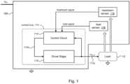
- Fig. 1 shows a circuit 100 in accordance with the present disclosure.
- the circuit 100 comprises a driver stage 112 having a drive output 112a that can be connected to drive a load 10.
- the load 10 may be any kind of a load.
- the load 10 may be an LED flash component of a camera; e.g., a digital camera or a camera in a portable computing device such as a computer tablet, a smartphone, and so on.
- a control circuit 114 provides a control signal 114a that is used to control operation of the driver stage 112.
- the control circuit 114 is configured with the driver stage 112 as a feedback control loop 110, with the driver output 112a feeding back to an input (e.g., 1 st input) of the control circuit.
- a response characteristic of the control loop 110 is set or otherwise altered in accordance with a signal indicative of the headroom voltage of the circuit 100 during operation when the circuit is driving the load 10.
- Headroom voltage refers to the voltage drop between the driver's voltage supply (e.g., V IN ) and the output voltage (e.g., V OUT ) of the driver 112; e.g., V IN - V OUT .
- circuit 100 includes a headroom sensing circuit 116 that senses a headroom of the circuit.
- the headroom sensing circuit 116 produces a headroom signal that is indicative of or otherwise representative of the headroom voltage of circuit 100.
- the headroom signal is provided to another input (e.g., 2 nd input) of the control circuit 114 to affect the response characteristic of the control loop 110. This aspect of the present disclosure will be discussed in more detail below.
- the response characteristic of the control loop 110 is further set or otherwise altered in accordance with a signal indicative of electrical loading on the circuit 100 due to load 10 during operation; e.g., electrical loading may be represented by the current flowing through the load.
- circuit 100 includes a load sensing circuit 118 that generates a load signal indicative of or otherwise representative of the electrical loading on the circuit.
- the load signal is provided to another input (e.g., 3 rd input) of the control circuit 114 to affect the response characteristic of the control loop 110.
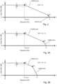
- the response characteristic of the control loop 110 may be represented by a frequency response curve 200 (e.g., a Bode plot).
- the response characteristic of the control loop 110 may be characterized by a gain (sometimes referred to as the closed loop gain) that varies with frequency, as illustrated in the frequency response curve 200.
- the response characteristic of the control loop 110 may be further characterized by a bandwidth (f bandwidth ), which is conventionally defined as the frequency at which the closed loop gain falls by -3 dB.
- f bandwidth bandwidth
- the plot shown in Fig. 2 is a straight-line plot of the actual response characteristic, which is continuous and has a 3 dB drop-off at the pole position P D .
- the frequency response curve 200 shown in Fig. 2 represents poles P D , P L of the response characteristic of the control loop 110.
- the response characteristic of control loop 110 may include any number and combination of poles and zeroes.
- the lowest frequency pole P D is sometimes referred to as the "dominant pole" because it dominates the effect of any higher frequency poles.
- the dominant pole typically defines the bandwidth of the response characteristic of the control loop 110.
- the load 10 that is driven by the driver stage 112 can affect the response characteristic of the control loop 110.
- the load 10 introduces an external pole P L to the frequency response curve of the control loop 110.
- the location or position of external pole P L depends on the size of the load 10 (e.g., expressed as an impedance Z). This effect is illustrated in Figs. 2, 2A, and 2B for different sized loads.
- Figs. 2, 2A, and 2B further illustrate that as the size of the load 10 increases (e.g., increasing impedance Z), the external pole P L moves closer to the dominant pole P D .
- each non-dominant pole closer than a decade away from the unity gain bandwidth of the feedback loop will reduce phase margin, which can ultimately degrade the control loop stability.
- the effect of the external pole on stable operation of the control loop 110 can be small; e.g., the location of external pole P L in Fig. 2 may be sufficiently far away from dominant pole P D so that the control loop 110 will be stable.
- the external pole P Lb may be close enough to the dominant pole P D that the phase margin is so small that unstable operation can result.
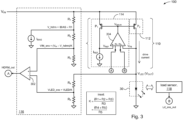
- the load may be an LED flash unit 30, such as might be found in digital cameras, portable computing devices, smart phones, etc.
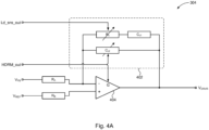
- the driver stage 112 may comprise a transistor P 2 , such as a power MOSFET for example.
- the transistor P 2 may provide a drive current from the supply voltage V IN to the LED flash unit 30.
- the control circuit 114 may comprise an OP amp 304 and a constant current source I REF .
- the control circuit 114 may further include a current mirror, comprising a transistor P 1 and the driver stage transistor P 2 , that is driven by the output V DRVR of OP amp 304.
- the driver stage 112 and control circuit 114 constitutes the control loop 110.
- the OP amp 304 in control circuit 114 may control the driver stage transistor P 2 in a feedback loop by regulating the drive current (provided as feedback voltage V FB ) based on a reference provided by the constant current source I REF (provided as V REF ).
- the constant current source I REF may be a small current source (e.g., 10 ⁇ A).
- the device dimensions of P 1 and P 2 in the current mirror may be designed to provide a suitable P 1 /P 2 current ratio in order to provide a suitable drive current to operate the LED flash unit 30.
- the P 1 /P 2 current ratio may be 1:10,000, giving a current gain of 10,000 at P 2 . It will be appreciated of course that in other embodiments, P 1 and P 2 can be designed to provide any suitable current gain.
- the headroom sensing circuit 116 generates a headroom signal indicative of or otherwise representative of the headroom voltage of the circuit 100.
- the headroom sensing circuit 116 may comprise a comparator 302 to compare the driver stage output voltage V OUT provided to the load (e.g., LED flash unit 30) against the supply voltage (e.g., V IN ).
- the headroom signal HDRM_out produced by the headroom sensing circuit 116 is thus representative of the headroom voltage of the circuit 100 and is feed into the control circuit 114.
- HDRM_out feeds into a control input IN 1 of the OP amp 304 of control circuit 114.
- resistor divider networks may be used to reduce the voltage levels that feed into comparator 302.
- the output voltage V OUT on the load 30 may be divided down by the resistor divider comprising R 4 and R 5 .
- the supply voltage V IN can be divided down in similar fashion as described below.
- the headroom sensing circuit 116 may include a programmable current source I BIAS .
- the voltage level V_hdrm can be viewed as defining a headroom voltage threshold.
- Resistors R 2 and R 3 then divide down the headroom voltage threshold.
- the inset in Fig. 3 defines the constant K, which in a particular embodiment also sets forth a relationship among the resistance values of resistors R 1 - R 5 .
- the load that is being driven by the driver stage 112 can change, depending what the load is, how it is being used, etc.; for example, an LED flash device 30 can operate in different modes; e.g., flash, strobe, etc.
- the size of the load can affect the response characteristic of the control loop 110.
- the load sensing circuit 118 produces a signal Ld_sns_out that represents the drive current from the driver stage 112 that feeds into the control circuit 114.
- the Ld_sns_out signal feeds into a control input IN 2 of the OP amp 304 of control circuit 114.
- the load sensing circuit 118 may comprise a current sensor.
- load sensing circuit 118' may comprise a mirrored sense transistor P sense that mirrors the current flow through the driver stage transistor P 2 .
- a comparator 306 may compare the current flow through P sense against a reference and output a signal Ld_sns_out that represents the level of the drive current flowing into the load 30.
- the load sensing circuit 118 may be load current programming circuit (not shown) that programs the load current, and the Ld_sns_out signal may be based on a parameter (e.g., stored in a programming register) used to program the load current.
- the response characteristic of the control loop 110 is set based on the headroom signal HDRM_out, or the load signal Ld_sns_out, or both.
- the HDRM_out signal is used to set the gain of the response characteristic, or the bandwidth of the response characteristic, or both.
- the Ld_sns_out signal is used to set the position of a zero of the response characteristic. As will be discussed below, this can improve stability in the control loop 110 as changes in the headroom voltage and loading conditions (e.g., current load) occur during operation of circuit 100.
- OP amp 304 illustrates how the HDRM_out and Ld_sns_out signals are used to set the response characteristic of control loop 110.
- the response characteristic of the control loop 110 may be set by setting circuit elements in the OP amp 304.
- the OP amp 304 may comprise an opamp device 404 having an inverting input and a non-inverting input.
- the reference voltage V REF may be connected to the non-inverting input through resistor R B .
- the feedback voltage V FB may be connected to the inverting input through resistor R A .
- the opamp device 404 may include a gain control input G that varies the gain of the opamp device.
- the HDRM_out signal may be coupled directly to or otherwise connected to the gain control input G, thereby allowing the HDRM_out signal to control the gain of the opamp device 404.
- circuit element Z 1 may represent a wire for a direct connection of the HDRM_out signal to the gain control input G, or Z 1 may represent some intervening electronic circuitry that can provide gain control as some function of the HDRM_out signal.
- circuit element Z 2 may represent a wire or some appropriate intervening electronic circuitry.
- the OP amp 304 may include a compensation network 402 of any suitable design.
- the response characteristic (e.g., transfer function H(s) ) of the control loop 110 may be expressed in terms of the circuit elements comprising the compensation network.
- the compensation network 402 may comprise one or more circuit elements that can be adjusted or otherwise varied using the HDRM_out signal and/or the Ld_sns_out signal in order to vary the response characteristic of control loop 110.
- the compensation network 402 may comprise a resistor element Rc connected in series with a capacitor element C C1 , and a shunt capacitor C C2 connected in parallel with the R C /C C1 pair.
- the resistor element Rc may provide a selectable resistance. Setting the resistance value of resistor Rc can set the position of a zero in the response characteristic of control loop 110.
- the capacitor C C2 provides a selectable capacitance. Setting the capacitance value of capacitor C C2 can set the position of the dominant pole in the response characteristic of control loop 110.
- the HDRM_out signal may be coupled directly to or otherwise connected to a selector input of the variable capacitor C C2 .
- circuit element Z 1 may represent a wire or some appropriate intervening electronic circuitry and likewise, circuit element Z 3 may represent a wire or some intervening electronic circuitry. Accordingly, the HDRM_out signal may be used to set the dominant pole position of the response characteristic of control loop 110.
- Ld_sns_out signal may be coupled directly or otherwise connected to a selector input of the variable resistor Rc.
- Circuit element Z 4 may represent a wire for a direct connection of the Ld_sns_out signal to the selector input of the variable resistor Rc, or Z 4 may represent some intervening electronic circuitry that can set resistor Rc as some function of the Ld_sns_out signal. Accordingly, the Ld_sns_out signal may be used to set a zero position of the response characteristic of control loop 110.
- circuit elements Z 1 - Z 4 are wires representing straight through connections, such as illustrated for example in Fig. 4A .
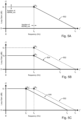
- frequency response curves 502 - 508 can be used to illustrate the effects on the response characteristic of control loop 110 when the headroom signal HDRM_out is applied in accordance with the present disclosure.
- the frequency response curve 502 in Fig. 5A represents a response characteristic of control loop 110 having a gain G1 and bandwidth f b as determined by the dominant pole P D .
- Fig. 5A illustrates that the headroom signal HDRM_out varies the gain and/or the dominant pole position (and hence the bandwidth) of the response characteristic.
- Fig. 5B shows how the frequency response curve 504 changes if just the gain is varied, for example, if the gain is reduced to G 2 ⁇ G 1 .
- the HDRM_out signal can be used to reduce the gain in order to improve stability in the control loop 110.
- the HDRM_out signal can control the gain of the opamp device 404 to vary the gain of the frequency response curve. Reducing the gain brings the unity gain bandwidth of the control loop 110 back from frequency f 1 to frequency f 2 . This improves stability if non-dominant poles exist within a decade or closer to f 1 .
- Fig. 5C shows how the frequency response curve 506 changes if just the dominant pole is varied, for example, from f b to f b ' ⁇ f b . Since the dominant pole determines the bandwidth, varying the dominant pole (e.g., P D to P D ') has the effect of varying the bandwidth of the response characteristic.
- the HDRM_out signal when the headroom voltage exceeds the threshold voltage, can be used to reduce the bandwidth in order to improve stability in the control loop 110. Conversely, when the headroom voltage falls below the threshold voltage, the HDRM_out signal can be used to increase the bandwidth to improve the response time of the control loop 110.
- the HDRM_out signal can control the value of the variable capacitor C C2 to vary the dominant pole position of the frequency response curve.
- the HDRM_out signal may control both the gain and the dominant pole position (i.e., bandwidth) of the response characteristic of control loop 110.
- the frequency response curve 508 shown in Fig. 5D illustrates an example in which the gain and bandwidth are reduced.
- the HDRM_out signal when the headroom voltage exceeds the threshold voltage, the HDRM_out signal can be used to reduce both the gain and the bandwidth of the response characteristic in order to improve stability in the control loop 110.
- the HDRM_out signal can be used to increase the gain and bandwidth to improve the response time of the control loop 110.
- the gain and bandwidth may change together, as HDRM_out changes. In other embodiments, the gain and bandwidth may be varied independently of each other.
- circuit elements Z 1 - Z 3 may be suitable control circuitry to isolate the HDRM_out signal from the gain control input and capacitor C C2 for independent operation.
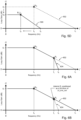
- frequency response curves 602, 604 can be used to illustrate the effects on the response characteristic of control loop 110 when the load signal Ld_sns_out is applied in accordance with the present disclosure.
- the load 10 e.g. LED flash unit 30, Fig. 3
- the response characteristic of the control loop 110 without a load is represented by the frequency response curve 602.
- an external pole P L due to the load may be introduced, which may result in frequency response curve 604.
- the additional drop off occurring a frequency f L reduces stability of the control loop 110 due to a decrease in phase margin.
- the Ld_sns_out signal is used to set a zero position of an internal zero in the control loop 110 to compensate for the external pole P L .
- the Ld_sns_out signal can control the value of variable resistor Rc to vary an internal zero of the response characteristic. This effect is illustrated in Fig. 6B , where the Ld_sns_out signal can set the zero position of an internal zero Z L to cancel the effect of the external pole P L and eliminate the drop off at frequency f L to improve stability.
- the load may be such as to introduce external pole P a to the response characteristic; in another situation, the load may be such as to introduce a different external pole, e.g., P b , to the response characteristic, and so on.
- the response characteristic of the control loop 110 changes.
- the stability of the control loop 110 can therefore vary according to the load, as illustrated by the frequency response curves, 612a, 612, b, 612c, 612d.
- designing a control circuit 114 ( Fig. 1 ) to maintain stability under any load condition can be challenging, since the designer has no control over what load the circuit 100 will be connected to or how the load may change during operation.
- the load sensor 118 produces a Ld_sns_out signal that is representative of or otherwise tracks the load.
- the Ld_sns_out signal can be used to adjust an internal zero of the control loop 110 (e.g., via variable resistor Rc) to compensate for varying external poles resulting from varying loads, and thus improve stability in the control loop 110 as represented by the frequency response curve 612. This effect is illustrated in Fig. 6D , which illustrates that the internal zero can vary to track the external pole as the load varies.
- circuits in accordance with the present disclosure allow for automatic adjustment of the loop gain and/or dominant pole position of the control loop based on voltage headroom during operation, when a load is being driven.
- circuits in accordance with the present disclosure allow for automatically varying the zero position of an internal zero of the control loop based on load condition of the load being driven by the circuit.
Landscapes
- Amplifiers (AREA)
- Dc-Dc Converters (AREA)
- Control Of Electric Motors In General (AREA)
- Steering Control In Accordance With Driving Conditions (AREA)
- Circuit Arrangement For Electric Light Sources In General (AREA)
- Continuous-Control Power Sources That Use Transistors (AREA)
Priority Applications (1)
| Application Number | Priority Date | Filing Date | Title |
|---|---|---|---|
| EP23212750.6A EP4326006A3 (en) | 2014-06-02 | 2015-05-18 | Adaptive stability control for a driver circuit |
Applications Claiming Priority (2)
| Application Number | Priority Date | Filing Date | Title |
|---|---|---|---|
| US14/293,489 US9190986B1 (en) | 2014-06-02 | 2014-06-02 | Adaptive stability control for a driver circuit |
| PCT/US2015/031381 WO2015187351A1 (en) | 2014-06-02 | 2015-05-18 | Adaptive stability control for a driver circuit |
Related Child Applications (1)
| Application Number | Title | Priority Date | Filing Date |
|---|---|---|---|
| EP23212750.6A Division EP4326006A3 (en) | 2014-06-02 | 2015-05-18 | Adaptive stability control for a driver circuit |
Publications (2)
| Publication Number | Publication Date |
|---|---|
| EP3150028A1 EP3150028A1 (en) | 2017-04-05 |
| EP3150028B1 true EP3150028B1 (en) | 2023-11-29 |
Family
ID=53298606
Family Applications (2)
| Application Number | Title | Priority Date | Filing Date |
|---|---|---|---|
| EP15727508.2A Active EP3150028B1 (en) | 2014-06-02 | 2015-05-18 | Adaptive stability control for a driver circuit |
| EP23212750.6A Pending EP4326006A3 (en) | 2014-06-02 | 2015-05-18 | Adaptive stability control for a driver circuit |
Family Applications After (1)
| Application Number | Title | Priority Date | Filing Date |
|---|---|---|---|
| EP23212750.6A Pending EP4326006A3 (en) | 2014-06-02 | 2015-05-18 | Adaptive stability control for a driver circuit |
Country Status (5)
| Country | Link |
|---|---|
| US (2) | US9190986B1 (enExample) |
| EP (2) | EP3150028B1 (enExample) |
| JP (1) | JP2017518573A (enExample) |
| CN (1) | CN106471739B (enExample) |
| WO (1) | WO2015187351A1 (enExample) |
Families Citing this family (5)
| Publication number | Priority date | Publication date | Assignee | Title |
|---|---|---|---|---|
| US10187806B2 (en) * | 2015-04-14 | 2019-01-22 | ETAK Systems, LLC | Systems and methods for obtaining accurate 3D modeling data using multiple cameras |
| DE102018205590B4 (de) * | 2018-04-12 | 2025-08-14 | Inventronics Gmbh | LEISTUNGSVERSORGUNGSVORRICHTUNG UND KOMMUNIKATIONSSYSTEM FÜR BELEUCHTUNGSSYSTEME MIT DERSELBEN, SOWIE vERFAHREN ZUR SPANNUNGSVERSORGUNG EINER ELEKTRISCHEN LAST |
| CN109587871B (zh) * | 2018-10-11 | 2021-07-20 | 威马智慧出行科技(上海)有限公司 | 一种灯光指示系统及其控制方法 |
| CN111200430B (zh) * | 2018-11-19 | 2023-01-13 | 马克西姆综合产品公司 | 驱动器电路系统及其相关方法 |
| CN112491266B (zh) * | 2019-09-10 | 2025-06-20 | 三垦电气株式会社 | 驱动器电路和电源 |
Citations (3)
| Publication number | Priority date | Publication date | Assignee | Title |
|---|---|---|---|---|
| US5945818A (en) * | 1997-02-28 | 1999-08-31 | Stmicroelectronics, Inc. | Load pole stabilized voltage regulator circuit |
| US20070241730A1 (en) * | 2006-04-14 | 2007-10-18 | Semiconductor Component Industries, Llc | Linear regulator and method therefor |
| US20120013317A1 (en) * | 2010-07-13 | 2012-01-19 | Ricoh Company, Ltd. | Constant voltage regulator |
Family Cites Families (22)
| Publication number | Priority date | Publication date | Assignee | Title |
|---|---|---|---|---|
| US6300749B1 (en) * | 2000-05-02 | 2001-10-09 | Stmicroelectronics S.R.L. | Linear voltage regulator with zero mobile compensation |
| TWI220022B (en) * | 2002-05-27 | 2004-08-01 | Richtek Technology Corp | Current sensing apparatus and method |
| US7023271B1 (en) * | 2004-03-31 | 2006-04-04 | Marvell International Ltd. | Variable-gain constant-bandwidth transimpedance amplifier |
| US7903058B1 (en) | 2005-01-21 | 2011-03-08 | National Semiconductor Corporation | Forward LED voltage monitoring for optimizing energy efficient operation of an LED driver circuit |
| US20060186870A1 (en) | 2005-02-07 | 2006-08-24 | California Micro Devices | Regulating switching regulators by load monitoring |
| US8299767B1 (en) | 2006-08-18 | 2012-10-30 | Picor Corporation | Dynamic safe operating area control |
| US7466195B2 (en) * | 2007-05-18 | 2008-12-16 | Quantance, Inc. | Error driven RF power amplifier control with increased efficiency |
| US8115414B2 (en) * | 2008-03-12 | 2012-02-14 | Freescale Semiconductor, Inc. | LED driver with segmented dynamic headroom control |
| US7843180B1 (en) * | 2008-04-11 | 2010-11-30 | Lonestar Inventions, L.P. | Multi-stage linear voltage regulator with frequency compensation |
| US7759912B2 (en) * | 2008-05-13 | 2010-07-20 | Micrel, Inc. | Adaptive compensation scheme for LC circuits in feedback loops |
| US8143868B2 (en) * | 2008-09-15 | 2012-03-27 | Mediatek Singapore Pte. Ltd. | Integrated LDO with variable resistive load |
| US9491822B2 (en) * | 2010-10-01 | 2016-11-08 | Intersil Americas LLC | LED driver with adaptive dynamic headroom voltage control |
| US10178716B2 (en) | 2010-11-08 | 2019-01-08 | Nxp B.V. | LED driver circuit and method |
| KR20120053783A (ko) | 2010-11-18 | 2012-05-29 | 삼성전자주식회사 | 발광 다이오드 구동회로, 발광 다이오드 구동방법 및 이를 포함하는 발광 다이오드 시스템 |
| KR20120055284A (ko) * | 2010-11-23 | 2012-05-31 | 삼성전자주식회사 | 발광 다이오드 구동회로, 발광 다이오드 구동방법 및 이를 포함하는 발광 다이오드 시스템 |
| KR20120058159A (ko) * | 2010-11-29 | 2012-06-07 | 에스이티아이(주) | Led용 스텝다운 dc-dc 변환기와 이를 이용한 led 전원 공급 장치 및 그 방법 |
| US8921747B2 (en) * | 2011-03-14 | 2014-12-30 | Electrolux Home Products, Inc. | Electric heating appliance with AC-line filter with low leakage current |
| KR101873497B1 (ko) * | 2011-04-07 | 2018-07-03 | 삼성디스플레이 주식회사 | 발광 다이오드 구동 장치 |
| US8669711B2 (en) * | 2011-04-22 | 2014-03-11 | Crs Electronics | Dynamic-headroom LED power supply |
| WO2013016289A1 (en) * | 2011-07-26 | 2013-01-31 | Summit Microelectronics, Inc. | Switching regulator with variable compensation |
| EP2704300A1 (en) * | 2012-08-06 | 2014-03-05 | Zentrum Mikroelektronik Dresden AG | Method for controlling a power stage |
| US9231463B2 (en) * | 2012-08-06 | 2016-01-05 | Peter Oaklander | Noise resistant regulator including an encoded control signal |
-
2014
- 2014-06-02 US US14/293,489 patent/US9190986B1/en active Active
-
2015
- 2015-05-18 EP EP15727508.2A patent/EP3150028B1/en active Active
- 2015-05-18 CN CN201580028622.8A patent/CN106471739B/zh active Active
- 2015-05-18 WO PCT/US2015/031381 patent/WO2015187351A1/en not_active Ceased
- 2015-05-18 JP JP2016570035A patent/JP2017518573A/ja active Pending
- 2015-05-18 EP EP23212750.6A patent/EP4326006A3/en active Pending
- 2015-10-14 US US14/883,317 patent/US9635724B2/en active Active
Patent Citations (3)
| Publication number | Priority date | Publication date | Assignee | Title |
|---|---|---|---|---|
| US5945818A (en) * | 1997-02-28 | 1999-08-31 | Stmicroelectronics, Inc. | Load pole stabilized voltage regulator circuit |
| US20070241730A1 (en) * | 2006-04-14 | 2007-10-18 | Semiconductor Component Industries, Llc | Linear regulator and method therefor |
| US20120013317A1 (en) * | 2010-07-13 | 2012-01-19 | Ricoh Company, Ltd. | Constant voltage regulator |
Also Published As
| Publication number | Publication date |
|---|---|
| CN106471739A (zh) | 2017-03-01 |
| EP3150028A1 (en) | 2017-04-05 |
| US20150349752A1 (en) | 2015-12-03 |
| US9635724B2 (en) | 2017-04-25 |
| EP4326006A2 (en) | 2024-02-21 |
| CN106471739B (zh) | 2019-04-26 |
| US20160037603A1 (en) | 2016-02-04 |
| EP4326006A3 (en) | 2024-04-24 |
| WO2015187351A1 (en) | 2015-12-10 |
| JP2017518573A (ja) | 2017-07-06 |
| US9190986B1 (en) | 2015-11-17 |
Similar Documents
| Publication | Publication Date | Title |
|---|---|---|
| US10498234B2 (en) | Voltage regulator with nonlinear adaptive voltage position and control method thereof | |
| EP3150028B1 (en) | Adaptive stability control for a driver circuit | |
| US7402987B2 (en) | Low-dropout regulator with startup overshoot control | |
| US10951116B2 (en) | Voltage regulator with nonlinear adaptive voltage position and control method thereof | |
| US9337727B2 (en) | Circuitry to control a switching regulator | |
| US9152159B2 (en) | Power supply circuit and semiconductor device | |
| US7714551B2 (en) | High PSRR linear voltage regulator and control method thereof | |
| JP5014194B2 (ja) | ボルテージレギュレータ | |
| US10067521B2 (en) | Low dropout regulator with PMOS power transistor | |
| US20100244801A1 (en) | Controller for switching regulator, switching regulator and light source | |
| JP7368132B2 (ja) | シリーズレギュレータ | |
| US20080265856A1 (en) | Constant-voltage power circuit | |
| KR20150070952A (ko) | 볼티지 레귤레이터 | |
| KR20160075329A (ko) | 볼티지 레귤레이터 | |
| US7579813B2 (en) | Power regulator having a voltage regulator module and having a voltage buffer module to provide a constant voltage output | |
| CN108363450B (zh) | 一种供电电路、终端设备及其供电控制方法 | |
| US10054970B2 (en) | Adaptive gain control for voltage regulators | |
| US10097087B2 (en) | Power conversion including sensing a load current and adapting output voltage based on the load current | |
| KR100969964B1 (ko) | 저전력 특성을 갖는 저손실 전압 레귤레이터 | |
| KR102727748B1 (ko) | 열 분산 회로 및 이를 포함하는 레귤레이터 제어 회로 | |
| CN217282708U (zh) | 自调节恒压源供电电路 | |
| US10299330B1 (en) | Current regulator | |
| CN114860014B (zh) | 电压调节电路 | |
| JP4184410B2 (ja) | ドロッパ型電池電圧補償装置 |
Legal Events
| Date | Code | Title | Description |
|---|---|---|---|
| STAA | Information on the status of an ep patent application or granted ep patent |
Free format text: STATUS: THE INTERNATIONAL PUBLICATION HAS BEEN MADE |
|
| PUAI | Public reference made under article 153(3) epc to a published international application that has entered the european phase |
Free format text: ORIGINAL CODE: 0009012 |
|
| STAA | Information on the status of an ep patent application or granted ep patent |
Free format text: STATUS: REQUEST FOR EXAMINATION WAS MADE |
|
| 17P | Request for examination filed |
Effective date: 20161020 |
|
| AK | Designated contracting states |
Kind code of ref document: A1 Designated state(s): AL AT BE BG CH CY CZ DE DK EE ES FI FR GB GR HR HU IE IS IT LI LT LU LV MC MK MT NL NO PL PT RO RS SE SI SK SM TR |
|
| AX | Request for extension of the european patent |
Extension state: BA ME |
|
| DAV | Request for validation of the european patent (deleted) | ||
| DAX | Request for extension of the european patent (deleted) | ||
| STAA | Information on the status of an ep patent application or granted ep patent |
Free format text: STATUS: EXAMINATION IS IN PROGRESS |
|
| 17Q | First examination report despatched |
Effective date: 20200224 |
|
| REG | Reference to a national code |
Ref country code: DE Ref legal event code: R079 Free format text: PREVIOUS MAIN CLASS: H05B0033080000 Ipc: H05B0045370000 Ref country code: DE Ref legal event code: R079 Ref document number: 602015086721 Country of ref document: DE Free format text: PREVIOUS MAIN CLASS: H05B0033080000 Ipc: H05B0045370000 |
|
| GRAP | Despatch of communication of intention to grant a patent |
Free format text: ORIGINAL CODE: EPIDOSNIGR1 |
|
| RIC1 | Information provided on ipc code assigned before grant |
Ipc: H05B 45/395 20200101ALI20230523BHEP Ipc: H05B 45/37 20200101AFI20230523BHEP |
|
| STAA | Information on the status of an ep patent application or granted ep patent |
Free format text: STATUS: GRANT OF PATENT IS INTENDED |
|
| INTG | Intention to grant announced |
Effective date: 20230629 |
|
| GRAS | Grant fee paid |
Free format text: ORIGINAL CODE: EPIDOSNIGR3 |
|
| GRAA | (expected) grant |
Free format text: ORIGINAL CODE: 0009210 |
|
| STAA | Information on the status of an ep patent application or granted ep patent |
Free format text: STATUS: THE PATENT HAS BEEN GRANTED |
|
| AK | Designated contracting states |
Kind code of ref document: B1 Designated state(s): AL AT BE BG CH CY CZ DE DK EE ES FI FR GB GR HR HU IE IS IT LI LT LU LV MC MK MT NL NO PL PT RO RS SE SI SK SM TR |
|
| REG | Reference to a national code |
Ref country code: GB Ref legal event code: FG4D |
|
| REG | Reference to a national code |
Ref country code: CH Ref legal event code: EP |
|
| REG | Reference to a national code |
Ref country code: DE Ref legal event code: R096 Ref document number: 602015086721 Country of ref document: DE |
|
| REG | Reference to a national code |
Ref country code: IE Ref legal event code: FG4D |
|
| REG | Reference to a national code |
Ref country code: LT Ref legal event code: MG9D |
|
| REG | Reference to a national code |
Ref country code: NL Ref legal event code: MP Effective date: 20231129 |
|
| PG25 | Lapsed in a contracting state [announced via postgrant information from national office to epo] |
Ref country code: GR Free format text: LAPSE BECAUSE OF FAILURE TO SUBMIT A TRANSLATION OF THE DESCRIPTION OR TO PAY THE FEE WITHIN THE PRESCRIBED TIME-LIMIT Effective date: 20240301 |
|
| PG25 | Lapsed in a contracting state [announced via postgrant information from national office to epo] |
Ref country code: IS Free format text: LAPSE BECAUSE OF FAILURE TO SUBMIT A TRANSLATION OF THE DESCRIPTION OR TO PAY THE FEE WITHIN THE PRESCRIBED TIME-LIMIT Effective date: 20240329 |
|
| PG25 | Lapsed in a contracting state [announced via postgrant information from national office to epo] |
Ref country code: LT Free format text: LAPSE BECAUSE OF FAILURE TO SUBMIT A TRANSLATION OF THE DESCRIPTION OR TO PAY THE FEE WITHIN THE PRESCRIBED TIME-LIMIT Effective date: 20231129 |
|
| PG25 | Lapsed in a contracting state [announced via postgrant information from national office to epo] |
Ref country code: ES Free format text: LAPSE BECAUSE OF FAILURE TO SUBMIT A TRANSLATION OF THE DESCRIPTION OR TO PAY THE FEE WITHIN THE PRESCRIBED TIME-LIMIT Effective date: 20231129 |
|
| PG25 | Lapsed in a contracting state [announced via postgrant information from national office to epo] |
Ref country code: LT Free format text: LAPSE BECAUSE OF FAILURE TO SUBMIT A TRANSLATION OF THE DESCRIPTION OR TO PAY THE FEE WITHIN THE PRESCRIBED TIME-LIMIT Effective date: 20231129 Ref country code: IS Free format text: LAPSE BECAUSE OF FAILURE TO SUBMIT A TRANSLATION OF THE DESCRIPTION OR TO PAY THE FEE WITHIN THE PRESCRIBED TIME-LIMIT Effective date: 20240329 Ref country code: GR Free format text: LAPSE BECAUSE OF FAILURE TO SUBMIT A TRANSLATION OF THE DESCRIPTION OR TO PAY THE FEE WITHIN THE PRESCRIBED TIME-LIMIT Effective date: 20240301 Ref country code: ES Free format text: LAPSE BECAUSE OF FAILURE TO SUBMIT A TRANSLATION OF THE DESCRIPTION OR TO PAY THE FEE WITHIN THE PRESCRIBED TIME-LIMIT Effective date: 20231129 Ref country code: BG Free format text: LAPSE BECAUSE OF FAILURE TO SUBMIT A TRANSLATION OF THE DESCRIPTION OR TO PAY THE FEE WITHIN THE PRESCRIBED TIME-LIMIT Effective date: 20240229 |
|
| REG | Reference to a national code |
Ref country code: AT Ref legal event code: MK05 Ref document number: 1637446 Country of ref document: AT Kind code of ref document: T Effective date: 20231129 |
|
| PG25 | Lapsed in a contracting state [announced via postgrant information from national office to epo] |
Ref country code: NL Free format text: LAPSE BECAUSE OF FAILURE TO SUBMIT A TRANSLATION OF THE DESCRIPTION OR TO PAY THE FEE WITHIN THE PRESCRIBED TIME-LIMIT Effective date: 20231129 |
|
| PG25 | Lapsed in a contracting state [announced via postgrant information from national office to epo] |
Ref country code: SE Free format text: LAPSE BECAUSE OF FAILURE TO SUBMIT A TRANSLATION OF THE DESCRIPTION OR TO PAY THE FEE WITHIN THE PRESCRIBED TIME-LIMIT Effective date: 20231129 Ref country code: RS Free format text: LAPSE BECAUSE OF FAILURE TO SUBMIT A TRANSLATION OF THE DESCRIPTION OR TO PAY THE FEE WITHIN THE PRESCRIBED TIME-LIMIT Effective date: 20231129 Ref country code: PL Free format text: LAPSE BECAUSE OF FAILURE TO SUBMIT A TRANSLATION OF THE DESCRIPTION OR TO PAY THE FEE WITHIN THE PRESCRIBED TIME-LIMIT Effective date: 20231129 Ref country code: NO Free format text: LAPSE BECAUSE OF FAILURE TO SUBMIT A TRANSLATION OF THE DESCRIPTION OR TO PAY THE FEE WITHIN THE PRESCRIBED TIME-LIMIT Effective date: 20240229 Ref country code: NL Free format text: LAPSE BECAUSE OF FAILURE TO SUBMIT A TRANSLATION OF THE DESCRIPTION OR TO PAY THE FEE WITHIN THE PRESCRIBED TIME-LIMIT Effective date: 20231129 Ref country code: LV Free format text: LAPSE BECAUSE OF FAILURE TO SUBMIT A TRANSLATION OF THE DESCRIPTION OR TO PAY THE FEE WITHIN THE PRESCRIBED TIME-LIMIT Effective date: 20231129 Ref country code: HR Free format text: LAPSE BECAUSE OF FAILURE TO SUBMIT A TRANSLATION OF THE DESCRIPTION OR TO PAY THE FEE WITHIN THE PRESCRIBED TIME-LIMIT Effective date: 20231129 |
|
| PG25 | Lapsed in a contracting state [announced via postgrant information from national office to epo] |
Ref country code: DK Free format text: LAPSE BECAUSE OF FAILURE TO SUBMIT A TRANSLATION OF THE DESCRIPTION OR TO PAY THE FEE WITHIN THE PRESCRIBED TIME-LIMIT Effective date: 20231129 |
|
| PG25 | Lapsed in a contracting state [announced via postgrant information from national office to epo] |
Ref country code: AT Free format text: LAPSE BECAUSE OF FAILURE TO SUBMIT A TRANSLATION OF THE DESCRIPTION OR TO PAY THE FEE WITHIN THE PRESCRIBED TIME-LIMIT Effective date: 20231129 Ref country code: CZ Free format text: LAPSE BECAUSE OF FAILURE TO SUBMIT A TRANSLATION OF THE DESCRIPTION OR TO PAY THE FEE WITHIN THE PRESCRIBED TIME-LIMIT Effective date: 20231129 |
|
| PG25 | Lapsed in a contracting state [announced via postgrant information from national office to epo] |
Ref country code: SK Free format text: LAPSE BECAUSE OF FAILURE TO SUBMIT A TRANSLATION OF THE DESCRIPTION OR TO PAY THE FEE WITHIN THE PRESCRIBED TIME-LIMIT Effective date: 20231129 |
|
| PG25 | Lapsed in a contracting state [announced via postgrant information from national office to epo] |
Ref country code: SM Free format text: LAPSE BECAUSE OF FAILURE TO SUBMIT A TRANSLATION OF THE DESCRIPTION OR TO PAY THE FEE WITHIN THE PRESCRIBED TIME-LIMIT Effective date: 20231129 Ref country code: SK Free format text: LAPSE BECAUSE OF FAILURE TO SUBMIT A TRANSLATION OF THE DESCRIPTION OR TO PAY THE FEE WITHIN THE PRESCRIBED TIME-LIMIT Effective date: 20231129 Ref country code: RO Free format text: LAPSE BECAUSE OF FAILURE TO SUBMIT A TRANSLATION OF THE DESCRIPTION OR TO PAY THE FEE WITHIN THE PRESCRIBED TIME-LIMIT Effective date: 20231129 Ref country code: IT Free format text: LAPSE BECAUSE OF FAILURE TO SUBMIT A TRANSLATION OF THE DESCRIPTION OR TO PAY THE FEE WITHIN THE PRESCRIBED TIME-LIMIT Effective date: 20231129 Ref country code: EE Free format text: LAPSE BECAUSE OF FAILURE TO SUBMIT A TRANSLATION OF THE DESCRIPTION OR TO PAY THE FEE WITHIN THE PRESCRIBED TIME-LIMIT Effective date: 20231129 Ref country code: DK Free format text: LAPSE BECAUSE OF FAILURE TO SUBMIT A TRANSLATION OF THE DESCRIPTION OR TO PAY THE FEE WITHIN THE PRESCRIBED TIME-LIMIT Effective date: 20231129 Ref country code: CZ Free format text: LAPSE BECAUSE OF FAILURE TO SUBMIT A TRANSLATION OF THE DESCRIPTION OR TO PAY THE FEE WITHIN THE PRESCRIBED TIME-LIMIT Effective date: 20231129 Ref country code: AT Free format text: LAPSE BECAUSE OF FAILURE TO SUBMIT A TRANSLATION OF THE DESCRIPTION OR TO PAY THE FEE WITHIN THE PRESCRIBED TIME-LIMIT Effective date: 20231129 |
|
| PG25 | Lapsed in a contracting state [announced via postgrant information from national office to epo] |
Ref country code: PT Free format text: LAPSE BECAUSE OF FAILURE TO SUBMIT A TRANSLATION OF THE DESCRIPTION OR TO PAY THE FEE WITHIN THE PRESCRIBED TIME-LIMIT Effective date: 20240401 |
|
| PG25 | Lapsed in a contracting state [announced via postgrant information from national office to epo] |
Ref country code: PT Free format text: LAPSE BECAUSE OF FAILURE TO SUBMIT A TRANSLATION OF THE DESCRIPTION OR TO PAY THE FEE WITHIN THE PRESCRIBED TIME-LIMIT Effective date: 20240401 |
|
| REG | Reference to a national code |
Ref country code: DE Ref legal event code: R097 Ref document number: 602015086721 Country of ref document: DE |
|
| PLBE | No opposition filed within time limit |
Free format text: ORIGINAL CODE: 0009261 |
|
| STAA | Information on the status of an ep patent application or granted ep patent |
Free format text: STATUS: NO OPPOSITION FILED WITHIN TIME LIMIT |
|
| PG25 | Lapsed in a contracting state [announced via postgrant information from national office to epo] |
Ref country code: SI Free format text: LAPSE BECAUSE OF FAILURE TO SUBMIT A TRANSLATION OF THE DESCRIPTION OR TO PAY THE FEE WITHIN THE PRESCRIBED TIME-LIMIT Effective date: 20231129 |
|
| PG25 | Lapsed in a contracting state [announced via postgrant information from national office to epo] |
Ref country code: SI Free format text: LAPSE BECAUSE OF FAILURE TO SUBMIT A TRANSLATION OF THE DESCRIPTION OR TO PAY THE FEE WITHIN THE PRESCRIBED TIME-LIMIT Effective date: 20231129 |
|
| 26N | No opposition filed |
Effective date: 20240830 |
|
| REG | Reference to a national code |
Ref country code: CH Ref legal event code: PL |
|
| PG25 | Lapsed in a contracting state [announced via postgrant information from national office to epo] |
Ref country code: MC Free format text: LAPSE BECAUSE OF FAILURE TO SUBMIT A TRANSLATION OF THE DESCRIPTION OR TO PAY THE FEE WITHIN THE PRESCRIBED TIME-LIMIT Effective date: 20231129 |
|
| PG25 | Lapsed in a contracting state [announced via postgrant information from national office to epo] |
Ref country code: LU Free format text: LAPSE BECAUSE OF NON-PAYMENT OF DUE FEES Effective date: 20240518 |
|
| PG25 | Lapsed in a contracting state [announced via postgrant information from national office to epo] |
Ref country code: MC Free format text: LAPSE BECAUSE OF FAILURE TO SUBMIT A TRANSLATION OF THE DESCRIPTION OR TO PAY THE FEE WITHIN THE PRESCRIBED TIME-LIMIT Effective date: 20231129 Ref country code: LU Free format text: LAPSE BECAUSE OF NON-PAYMENT OF DUE FEES Effective date: 20240518 Ref country code: CH Free format text: LAPSE BECAUSE OF NON-PAYMENT OF DUE FEES Effective date: 20240531 |
|
| REG | Reference to a national code |
Ref country code: BE Ref legal event code: MM Effective date: 20240531 |
|
| PG25 | Lapsed in a contracting state [announced via postgrant information from national office to epo] |
Ref country code: IE Free format text: LAPSE BECAUSE OF NON-PAYMENT OF DUE FEES Effective date: 20240518 |
|
| PG25 | Lapsed in a contracting state [announced via postgrant information from national office to epo] |
Ref country code: BE Free format text: LAPSE BECAUSE OF NON-PAYMENT OF DUE FEES Effective date: 20240531 |
|
| PGFP | Annual fee paid to national office [announced via postgrant information from national office to epo] |
Ref country code: DE Payment date: 20250409 Year of fee payment: 11 |
|
| PGFP | Annual fee paid to national office [announced via postgrant information from national office to epo] |
Ref country code: FR Payment date: 20250409 Year of fee payment: 11 |
|
| PG25 | Lapsed in a contracting state [announced via postgrant information from national office to epo] |
Ref country code: CY Free format text: LAPSE BECAUSE OF FAILURE TO SUBMIT A TRANSLATION OF THE DESCRIPTION OR TO PAY THE FEE WITHIN THE PRESCRIBED TIME-LIMIT; INVALID AB INITIO Effective date: 20150518 |
|
| PG25 | Lapsed in a contracting state [announced via postgrant information from national office to epo] |
Ref country code: HU Free format text: LAPSE BECAUSE OF FAILURE TO SUBMIT A TRANSLATION OF THE DESCRIPTION OR TO PAY THE FEE WITHIN THE PRESCRIBED TIME-LIMIT; INVALID AB INITIO Effective date: 20150518 |
|
| PG25 | Lapsed in a contracting state [announced via postgrant information from national office to epo] |
Ref country code: FI Free format text: LAPSE BECAUSE OF FAILURE TO SUBMIT A TRANSLATION OF THE DESCRIPTION OR TO PAY THE FEE WITHIN THE PRESCRIBED TIME-LIMIT Effective date: 20231129 |
|
| PGFP | Annual fee paid to national office [announced via postgrant information from national office to epo] |
Ref country code: GB Payment date: 20260320 Year of fee payment: 12 |